EP2093881A1 - Elastic wave filter device - Google Patents
Elastic wave filter device Download PDFInfo
- Publication number
- EP2093881A1 EP2093881A1 EP07831617A EP07831617A EP2093881A1 EP 2093881 A1 EP2093881 A1 EP 2093881A1 EP 07831617 A EP07831617 A EP 07831617A EP 07831617 A EP07831617 A EP 07831617A EP 2093881 A1 EP2093881 A1 EP 2093881A1
- Authority
- EP
- European Patent Office
- Prior art keywords
- acoustic wave
- filter device
- band
- wave filter
- resonators
- Prior art date
- Legal status (The legal status is an assumption and is not a legal conclusion. Google has not performed a legal analysis and makes no representation as to the accuracy of the status listed.)
- Granted
Links
Images





Classifications
-
- H—ELECTRICITY
- H03—ELECTRONIC CIRCUITRY
- H03H—IMPEDANCE NETWORKS, e.g. RESONANT CIRCUITS; RESONATORS
- H03H9/00—Networks comprising electromechanical or electro-acoustic elements; Electromechanical resonators
- H03H9/46—Filters
- H03H9/64—Filters using surface acoustic waves
- H03H9/6423—Means for obtaining a particular transfer characteristic
- H03H9/6433—Coupled resonator filters
- H03H9/6483—Ladder SAW filters
Definitions
- the present invention relates to acoustic wave filter devices using, for example, a surface acoustic wave filter or a boundary acoustic wave filter, and particularly relates to an acoustic wave filter device having a pass band lower than a trap band.
- one channel is divided into 13 segments. Of the 13 segments, one segment located at the center of one channel is used as a transmission band for mobile phones. Broadcasting using this one segment is so-called one-segment broadcasting, which uses a transmission band from 470 MHz to 770 MHz.
- Transmission bands for mobile phones may vary among different methods and communications companies. For example, a band of 800 MHz or more, such as from 830 MHz to 845 MHz or from 898 MHz to 924 MHz, a 1.7 GHz band, and a 1.9 GHz band are used. Some mobile phones are capable of receiving and even recording one-segment broadcasting. In such a mobile phone, if phone transmission is performed simultaneously with reception and recording of one-segment broadcasting, a received video image may be distorted due to the effect of transmitted radio waves. Accordingly, there is a demand for band rejection filters having a trap band equal to a transmission band of the mobile phone and having a pass band lower than the trap band.
- Patent Document 1 discloses an example of a surface acoustic wave filter device of band rejection type.
- Fig. 14 illustrates a circuit configuration of the surface acoustic wave filter device described in Patent Document 1.
- a surface acoustic wave filter device 501 has an input terminal 502 and an output terminal 503.
- An inductor 504 is inserted in a series arm connecting the input terminal 502 and the output terminal 503.
- a surface acoustic wave resonator 505 is connected between one end of the inductor 504 and a ground potential, while a surface acoustic wave resonator 506 is connected between the other end of the inductor 504 and the ground potential. That is, the inductor 504 and the two surface acoustic wave resonators 505 and 506 constitute a ⁇ -type filter circuit.
- resonance frequencies of the surface acoustic wave resonators 505 and 506 are placed in an attenuation band in intended filter characteristics, an electric signal at the resonance frequencies is lowered to the ground potential, and thus attenuation characteristics are obtained. That is, a trap band is defined by the resonance frequencies of the surface acoustic wave resonators 505 and 506.
- the resonance frequencies of the surface acoustic wave resonators 505 and 506 are placed in a frequency range where a trap is provided, and thus the trap band is defined.
- the electric signal at the resonance frequencies is lowered to the ground potential, the electric signal has a common inductance component on a piezoelectric substrate or a package included in the surface acoustic wave filter device 501.
- the signal leaks through the surface acoustic wave resonators 505 and 506, satisfactory attenuation characteristics cannot be achieved in the trap band.
- the surface acoustic wave filter device 501 is used as a band rejection filter for a reception stage of one-segment broadcasting in the mobile phone capable of receiving one-segment broadcasting, it is difficult to reliably attenuate transmitted radio waves of the mobile phone during reception or recording of one-segment broadcasting.
- An object of the present invention is to overcome the drawbacks of the conventional techniques described above, and to provide an acoustic wave filter device having steep attenuation characteristics in a region of a trap band near a pass band and capable of providing a large amount of attenuation.
- the present invention provides an acoustic wave filter device having a trap band and a pass band lower than the trap band.
- the acoustic wave filter device includes a plurality of inductors connected in series in a series arm having and connecting an input terminal and an output terminal, and a plurality of first acoustic wave resonators connected between the series arm and a ground potential.
- a plurality of filter circuits are arranged in a direction from the input terminal to the output terminal.
- Each of the plurality of filter circuits is composed of at least one of the plurality of inductors and the first acoustic wave resonators connected between the ground potential and respective ends of the at least one of the plurality of inductors.
- the acoustic wave filter device further includes a second acoustic wave resonator inserted in the series arm. In at least one of areas where the plurality of filter circuits are adjacent to each other, the adjacent filter circuits are electrically connected by the second acoustic wave resonator.
- the adjacent filter circuits are electrically connected by the second acoustic wave resonator. This can increase the amount of attenuation in the trap band and make it possible to provide steeper attenuation characteristics.
- first and second filter circuits may be provided as the plurality of filter circuits.
- the first and second filter circuits are electrically connected to each other by one second acoustic wave resonator, it is possible to provide a compact acoustic wave filter device having a simple circuit configuration.
- a resonance frequency of at least one of the plurality of first acoustic wave resonators is outside the trap band.
- an attenuation band other than the trap band can be formed at the resonance frequency of the at least one acoustic wave resonator. That is, it is possible to provide a filter device having a plurality of attenuation bands.
- the first acoustic wave resonator having the resonance frequency outside the trap band is connected between the output terminal and the ground potential.
- the first acoustic wave resonator having the resonance frequency outside the trap band becomes capacitive in the trap band, and an impedance of the first acoustic wave resonator increases.
- a leakage signal in the trap band is less likely to reach the output terminal via the first acoustic wave resonator having the resonance frequency outside the trap band. Therefore, it is possible to further increase the amount of attenuation in the attenuation band and further enhance the steepness of attenuation frequency characteristics.
- the acoustic wave filter device further includes a piezoelectric substrate, and the first and second acoustic wave resonators are formed on the piezoelectric substrate.
- an antiresonance frequency of the second acoustic wave resonator is set to be lower than resonance frequencies of the first acoustic wave resonators, the resonance frequencies defining the trap band. Therefore, it is possible to further improve the steepness of attenuation frequency characteristics in the range from the pass band to the trap band.
- a plurality of filter circuits are arranged in a direction from the input terminal to the output terminal.
- Each of the plurality of filter circuits is composed of at least one of the plurality of inductors and the first acoustic wave resonators connected between the ground potential and respective ends of the at least one of the plurality of inductors. Then, in at least one of areas where the plurality of filter circuits are adjacent to each other, the adjacent filter circuits are electrically connected by the second acoustic wave resonator.
- a fractional pass bandwidth as high as 50% or more can be realized, and it is possible to achieve steeper attenuation characteristics near the pass band and provide a larger amount of attenuation.
- acoustic wave filter device suitable for use as a band rejection filter having a trap band near a pass band and required to provide a large amount of attenuation in the trap band.
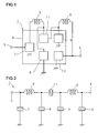
- Fig. 1 is a schematic plan view of an acoustic wave filter device according to a first embodiment of the present invention.
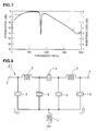
- Fig. 2 is a circuit diagram of Fig. 1 .
- An acoustic wave filter device 1 of the present embodiment is a surface acoustic wave filter device using surface acoustic waves.
- the acoustic wave filter device 1 includes a piezoelectric substrate 2.
- a Y-cut X-propagating LiNbO 3 substrate is used as the piezoelectric substrate 2.
- the piezoelectric substrate 2 may be a LiNbO 3 substrate having a different crystal orientation, a different piezoelectric single crystal substrate such as a piezoelectric LiTaO 3 or quartz substrate, or a piezoelectric ceramic substrate.
- a circuit configuration illustrated in Fig. 2 is realized by forming metal (such as Al or Cu) or alloy electrodes on the piezoelectric substrate 2.
- the acoustic wave filter device 1 has a series arm connecting an input terminal 3 and an output terminal 4.
- a plurality of inductors 5 and 6 are inserted in the series arm.
- a plurality of first acoustic wave resonators 7 to 11 are connected such that the series arm is connected to a ground potential. That is, the first acoustic wave resonator 7 is connected between the series arm and the ground potential to form one parallel arm.
- each of the other first acoustic wave resonators 8 to 10 forms one parallel arm.
- one inductor 5, the first acoustic wave resonator 7 connected between one end of the inductor 5 and the ground potential, and the first acoustic wave resonator 8 connected between the other end of the inductor 5 and the ground potential constitute a ⁇ -type first filter circuit.
- the inductor 6, the first acoustic wave resonator 9 connected between one end of the inductor 6 and the ground potential, and the first acoustic wave resonator 10 connected between the other end of the inductor 6 and the ground potential constitute a ⁇ -type second filter circuit.
- a second acoustic wave resonator 11 is inserted in the series arm to electrically connect the first and second filter circuits. In other words, in an area where the first and second filter circuits are adjacent to each other, the second acoustic wave resonator 11 is inserted in the series arm, and thus the adjacent first and second filter circuits are electrically connected to each other.
- the first acoustic wave resonators 7 to 10 and the second acoustic wave resonator 11 each are schematically represented by a rectangular frame.
- Each of the acoustic wave resonators is produced by forming an IDT electrode and a pair of reflectors on the piezoelectric substrate 2.
- the reflectors are arranged on both sides of the IDT electrode in a surface wave propagation direction.
- the electrode structure of each of the resonators is not particularly limited to this.
- a compact surface acoustic wave filter chip can be produced by forming the acoustic wave resonators 7 to 11 on one piezoelectric substrate 2.
- the inductors 5 and 6 are inductance components external to the piezoelectric substrate 2.
- the inductors 5 and 6 may be formed on the piezoelectric substrate 2 or provided by forming an inductance element section within the piezoelectric substrate 2.
- Fig. 3 shows impedance characteristics of the first acoustic wave resonators 7 to 10 and impedance characteristics of the second acoustic wave resonator 11.
- impedances at resonance frequencies of the first acoustic wave resonators 7 to 10 i.e., parallel arm resonators
- an impedance at an antiresonance frequency of the second acoustic wave resonator 11 i.e., series arm resonator
- the first and second filter circuits are connected to each other by the second acoustic wave resonator 11. As described below, this can increase the amount of attenuation in a region of the trap band near the pass band, and enhance the steepness of attenuation characteristics. This will be described in detail below.
- the surface acoustic wave filter device 501 described in Patent Document 1 cannot achieve satisfactory attenuation characteristics, probably due to the following reasons. That is, in the surface acoustic wave filter device 501 illustrated in Fig. 14 , the surface acoustic wave resonators 505 and 506 are connected by the inductor 504, in other words, by reactance. In this case, the resonance frequencies of the surface acoustic wave resonators 505 and 506 are used to obtain attenuation characteristics.
- the signal has a common inductance component between the surface acoustic wave resonator 505 or 506 and the ground potential.
- this common inductance component causes the signal at the resonance frequency of the surface acoustic wave resonator 505 to pass through a common inductance and the surface acoustic wave resonator 506, and to leak to the output terminal 503. This leads to degradation in attenuation characteristics.
- An inductance L in Fig. 15 represents an inductance inserted by wiring or the like between an electrode land connected to the ground potential of the acoustic wave filter device 1 and the ground potential.
- the first and second filter circuits are connected to each other by the second acoustic wave resonator 11, which is a series arm resonator.
- the attenuation band can be obtained by using the resonance frequencies of the first acoustic wave resonators 7 to 10, which are parallel arm resonators, and the antiresonance frequency of the second acoustic wave resonator 11, which is a series arm resonator.
- the antiresonance frequency of the second acoustic wave resonator 11 is close to the resonance frequencies of the first acoustic wave resonators 7 to 10. Therefore, although an electric signal at the resonance frequency of the first acoustic wave resonator 7 flows as indicated by arrows in Fig. 4 , this signal path is cut off by the second acoustic wave resonator 11. This can reduce signal leakage through the first acoustic wave resonators 7 and 8 to the output terminal. Thus, it is possible to obtain steep attenuation characteristics with a large amount of attenuation.
- An inductance L in Fig. 4 represents an inductance inserted by wiring or the like between an electrode land connected to the ground potential of the acoustic wave filter device 1 and the ground potential.
- Fig. 6 and Fig. 7 are graphs showing attenuation frequency characteristics of the acoustic wave filter device according to the present embodiment. As is apparent from Fig. 6 and Fig. 7 , a large amount of attenuation can be obtained at frequencies from 820 MHz to 860 MHz. As shown, steepness of attenuation frequency characteristics can be achieved in the range from the pass band lower than the trap band to the trap band.
- a transmission band in an RF stage is often defined as an attenuation band.
- the transmission band in the RF stage include an 800 MHz band, a 1.7 GHz band, and a 1.9 GHz band.
- the attenuation frequency characteristics shown in Fig. 6 and Fig. 7 in the present embodiment, a large amount of attenuation can be obtained in any of these frequency bands.
- the first and second filter circuits are connected to each other by the second acoustic wave resonator 11.
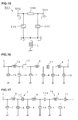
- three or more filter circuits may be arranged between the input terminal 3 and the output terminal 4.
- a third filter circuit is further arranged on the input side of the first and second filter circuits of the first embodiment.
- the third filter circuit is a ⁇ -type filter circuit composed of an inductance 12 and first acoustic wave resonators 13 and 14, which are parallel arm resonators. As illustrated in Fig. 13 , the third filter circuit is connected to the first filter circuit, with no second acoustic wave resonator therebetween.
- Fig. 16 is a circuit diagram illustrating another modification of the first embodiment.
- a third filter circuit is further arranged on the input side of the first and second filter circuits of the first embodiment.
- the third filter circuit is a ⁇ -type filter circuit composed of the inductance 12 and the first acoustic wave resonators 13 and 14, which are parallel arm resonators.
- the third filter circuit is connected to the input side of the first filter circuit via a reactance element 15, not an acoustic wave resonator.
- the reactance element 15 may be an inductor or a capacitor.
- Fig. 17 is a circuit diagram of such a preferable modification.
- the modified acoustic wave filter device illustrated in Fig. 17 is a multi-stage acoustic wave filter device formed by connecting a plurality of acoustic wave filter devices 1 of the first embodiment in the direction from the input terminal 3 toward an output terminal.
- Fig. 17 illustrates the acoustic wave filter device 1 in the first stage and part of an acoustic wave filter device 1A in the next stage.
- the acoustic wave filter device 1 and the acoustic wave filter device 1A are connected to each other via a second acoustic wave resonator 11A.
- the first and second filter circuits of the acoustic wave filter device 1 are connected to each other by the second acoustic wave resonator 11, and the second filter circuit of the acoustic wave filter device 1 and the first filter circuit of the acoustic wave filter device 1A in the next stage are electrically connected to each other by the second acoustic wave resonator 11A.
- the second acoustic wave resonator is provided in every area where two filter circuits are adjacent to each other. This makes it possible to more reliably achieve steep attenuation characteristics and provide a larger amount of attenuation in the attenuation band.
- two filter circuits be connected to one second acoustic wave resonator.
- This configuration makes it possible to produce the acoustic wave filter device 1 without significantly increasing the number of components. Thus, it is possible to reduce the number of components, mounting space, and costs.
- a leakage signal path is blocked by the second acoustic wave resonator 11.
- the first embodiment as indicated by arrows in Fig. 5 , it is possible that a signal having passed through the first acoustic wave resonator 7 and the first acoustic wave resonator 10 on the output terminal side leaks out.
- the flow of a signal having passed through the first acoustic wave resonator 7 and the first acoustic wave resonator 8 is blocked as described above, it is possible to achieve steep resonance characteristics and realize a large amount of attenuation in the rejection band.
- a signal having passed through the first acoustic wave resonator 7 and the first acoustic wave resonator 10 on the output terminal side may leak out.
- Fig. 8 is a circuit diagram of an acoustic wave filter device according to a second embodiment of the present invention. The acoustic wave filter device of the second embodiment is capable of preventing such signal leakage.
- An acoustic wave filter device 21 of the second embodiment is identical to the acoustic wave filter device 1 of the first embodiment in that it includes the first acoustic wave resonators 7 to 10, the second acoustic wave resonator 11, and the inductances 5 and 6.
- the acoustic wave filter device 21 differs from the acoustic wave filter device 1 in that, of the four first acoustic wave resonators 7 to 10, the first acoustic wave resonator 10 connected to the output terminal 3 has a resonance frequency that is different from those of the other first acoustic wave resonators 7 to 9 and is positioned away from the trap band of the acoustic wave filter device 21.
- the first acoustic wave resonator 10 functions simply as a capacitive element.
- Fig. 9 is a graph showing impedance characteristics of the four first acoustic wave resonators of the second embodiment. As shown in Fig.
- the second embodiment is preferable in that, as compared to the first embodiment, a larger amount of attenuation can be provided and steeper attenuation characteristics can be achieved.
- Fig. 10 is a graph showing attenuation frequency characteristics of the acoustic wave filter device 1 according to the first embodiment and the acoustic wave filter device 21 according to the second embodiment.
- a solid line represents a result of the second embodiment
- a broken line represents a result of the first embodiment.
- the second embodiment makes it possible to provide a larger amount of attenuation and achieve steeper attenuation characteristics than those in the case of the first embodiment.
- a plurality of first acoustic wave resonators that is, a plurality of parallel arm resonators can be selectively used as a resonator or a capacitive element in the trap band.
- band filters such as band rejection filters, capable of satisfying new market demands for having a plurality of trap bands near the pass band.
- band filters such as band rejection filters
- a plurality of trap frequency bands near the pass band of the acoustic wave filter device 21 may be used.
- the lowest trap frequency band is set as a trap band of the acoustic wave filter device 21.
- the other trap bands are defined by positioning, in the remaining trap frequency bands, the resonance frequency of the first acoustic wave resonator used as a capacitive element in the trap band.
- a plurality of trap bands can be defined by varying the resonance frequencies of the plurality of parallel arm resonators, that is, the plurality of first acoustic wave resonators. It is thus possible to produce a band rejection filter having a plurality of trap bands higher than the pass band.
- Fig. 11 is a graph showing attenuation characteristics observed when the inductance value of the inductors 5 and 6 varies ⁇ 5% in the acoustic wave filter device 21 of the second embodiment.
- a solid line represents filter characteristics corresponding to a standard inductance value
- a broken line represents filter characteristics observed when the inductance value of the inductors 5 and 6 is 5% higher than the standard inductance value
- an alternate long and short dashed line represents filter characteristics observed when the inductance value of the inductors 5 and 6 is 5% lower than the standard inductance value.
- the inductors 5 and 6 may be chip coil components 5A and 6A mounted on the piezoelectric substrate 2.
- the acoustic wave filter device 1 can be readily produced, for example, by surface-mounting the chip coil components on the piezoelectric substrate. Forming inductance elements on or within the piezoelectric substrate 2 is preferable in that it is possible to omit the process of mounting external components, such as the above-described chip coils, and reduce variations in characteristics caused by variations in mounting.
- An acoustic wave filter device of the third embodiment is identical to the acoustic wave filter device 1 of the first embodiment in that it includes the first acoustic wave resonators 7 to 10, the second acoustic wave resonator 11, and the inductances 5 and 6.
- a circuit diagram of the acoustic wave filter device according to the third embodiment is identical to the circuit diagram of the acoustic wave filter device 1 according to the first embodiment illustrated in Fig. 2 .
- the acoustic wave filter device of the third embodiment differs from the acoustic wave filter device 1 in terms of the relationship between the antiresonance frequency of the second acoustic wave resonator 11 (i.e., series arm resonator) and the resonance frequencies of the first acoustic wave resonators, the antiresonance and resonance frequencies defining the trap band.
- the antiresonance frequency of the second acoustic wave resonator 11 according to the first embodiment is set to a value between the maximum and minimum values among the resonance frequencies of the first acoustic wave resonators, the resonance frequencies defining the trap band
- the antiresonance frequency of the second acoustic wave resonator 11 according to the third embodiment is set to a value lower than the minimum value among the resonance frequencies of the first acoustic wave resonators.
- Table 1 shows the resonance and antiresonance frequencies of the first and second acoustic wave resonators of the acoustic wave filter device according to the third embodiment.
- an acoustic wave filter device according to a fourth embodiment of the present invention is produced.
- the acoustic wave filter device of the fourth embodiment has a configuration similar to that of the acoustic wave filter device of the first embodiment.
- Table 2 shows the resonance and antiresonance frequencies of the first and second acoustic wave resonators according to the fourth embodiment.
- Fig. 18 is a graph showing attenuation frequency characteristics of the acoustic wave filter device according to the third embodiment and the acoustic wave filter device according to the fourth embodiment.
- a solid line represents a result of the third embodiment
- a broken line represents a result of the fourth embodiment.
- the steepness of the attenuation frequency characteristics in the range from the pass band to the trap band is further improved.
- the antiresonance frequency of the second acoustic wave resonator be lower than the minimum value among the resonance frequencies of the first acoustic wave resonators, the resonance frequencies defining the trap band, and be higher than 0.95 time the minimum value. This is because if the antiresonance frequency of the second acoustic wave resonator is too far from the trap band, the amount of attenuation in the trap band becomes small.
- the surface acoustic wave filter devices have been described in the first to fourth embodiments. It is to be pointed out that the present invention is also applicable to boundary acoustic wave filter devices using boundary acoustic waves instead of surface acoustic waves.
Landscapes
- Physics & Mathematics (AREA)
- Acoustics & Sound (AREA)
- Surface Acoustic Wave Elements And Circuit Networks Thereof (AREA)
- Piezo-Electric Or Mechanical Vibrators, Or Delay Or Filter Circuits (AREA)
Abstract
Description
- The present invention relates to acoustic wave filter devices using, for example, a surface acoustic wave filter or a boundary acoustic wave filter, and particularly relates to an acoustic wave filter device having a pass band lower than a trap band.
- Up until now, various filter devices using acoustic waves, such as surface acoustic wave devices and boundary acoustic wave devices, have been proposed as band filters for communication apparatuses. For example, surface acoustic wave devices have been widely used as RF band filters for mobile phones.
- In recent years, digital terrestrial television broadcasting has been becoming widespread. In digital terrestrial broadcasting, one channel is divided into 13 segments. Of the 13 segments, one segment located at the center of one channel is used as a transmission band for mobile phones. Broadcasting using this one segment is so-called one-segment broadcasting, which uses a transmission band from 470 MHz to 770 MHz.
- Transmission bands for mobile phones may vary among different methods and communications companies. For example, a band of 800 MHz or more, such as from 830 MHz to 845 MHz or from 898 MHz to 924 MHz, a 1.7 GHz band, and a 1.9 GHz band are used. Some mobile phones are capable of receiving and even recording one-segment broadcasting. In such a mobile phone, if phone transmission is performed simultaneously with reception and recording of one-segment broadcasting, a received video image may be distorted due to the effect of transmitted radio waves. Accordingly, there is a demand for band rejection filters having a trap band equal to a transmission band of the mobile phone and having a pass band lower than the trap band.
-
Patent Document 1 discloses an example of a surface acoustic wave filter device of band rejection type.Fig. 14 illustrates a circuit configuration of the surface acoustic wave filter device described inPatent Document 1. - A surface acoustic
wave filter device 501 has aninput terminal 502 and anoutput terminal 503. Aninductor 504 is inserted in a series arm connecting theinput terminal 502 and theoutput terminal 503. A surfaceacoustic wave resonator 505 is connected between one end of theinductor 504 and a ground potential, while a surfaceacoustic wave resonator 506 is connected between the other end of theinductor 504 and the ground potential. That is, theinductor 504 and the two surfaceacoustic wave resonators - In the surface acoustic
wave filter device 501, resonance frequencies of the surfaceacoustic wave resonators acoustic wave resonators - Patent Document 1: Japanese Unexamined Patent Application Publication No.
2004-129238 - In the surface
acoustic wave device 501, the resonance frequencies of the surfaceacoustic wave resonators wave filter device 501. As a result, since the signal leaks through the surfaceacoustic wave resonators wave filter device 501 is used as a band rejection filter for a reception stage of one-segment broadcasting in the mobile phone capable of receiving one-segment broadcasting, it is difficult to reliably attenuate transmitted radio waves of the mobile phone during reception or recording of one-segment broadcasting. - An object of the present invention is to overcome the drawbacks of the conventional techniques described above, and to provide an acoustic wave filter device having steep attenuation characteristics in a region of a trap band near a pass band and capable of providing a large amount of attenuation.
- The present invention provides an acoustic wave filter device having a trap band and a pass band lower than the trap band. The acoustic wave filter device includes a plurality of inductors connected in series in a series arm having and connecting an input terminal and an output terminal, and a plurality of first acoustic wave resonators connected between the series arm and a ground potential. In the acoustic wave filter device, a plurality of filter circuits are arranged in a direction from the input terminal to the output terminal. Each of the plurality of filter circuits is composed of at least one of the plurality of inductors and the first acoustic wave resonators connected between the ground potential and respective ends of the at least one of the plurality of inductors. The acoustic wave filter device further includes a second acoustic wave resonator inserted in the series arm. In at least one of areas where the plurality of filter circuits are adjacent to each other, the adjacent filter circuits are electrically connected by the second acoustic wave resonator.
- In the acoustic wave filter device according to the present invention, preferably, in every area where filter circuits are adjacent to each other, the adjacent filter circuits are electrically connected by the second acoustic wave resonator. This can increase the amount of attenuation in the trap band and make it possible to provide steeper attenuation characteristics.
- In the acoustic wave filter device according to the present invention, only first and second filter circuits may be provided as the plurality of filter circuits. In this case, since the first and second filter circuits are electrically connected to each other by one second acoustic wave resonator, it is possible to provide a compact acoustic wave filter device having a simple circuit configuration.
- In the present invention, preferably, a resonance frequency of at least one of the plurality of first acoustic wave resonators is outside the trap band. In this case, since the first acoustic wave resonator whose resonance frequency is set to a value outside the trap band has a resonance frequency outside the trap band, an attenuation band other than the trap band can be formed at the resonance frequency of the at least one acoustic wave resonator. That is, it is possible to provide a filter device having a plurality of attenuation bands.
- More preferably, the first acoustic wave resonator having the resonance frequency outside the trap band is connected between the output terminal and the ground potential. In this case, the first acoustic wave resonator having the resonance frequency outside the trap band becomes capacitive in the trap band, and an impedance of the first acoustic wave resonator increases. Thus, a leakage signal in the trap band is less likely to reach the output terminal via the first acoustic wave resonator having the resonance frequency outside the trap band. Therefore, it is possible to further increase the amount of attenuation in the attenuation band and further enhance the steepness of attenuation frequency characteristics.
- In another specific aspect of the present invention, the acoustic wave filter device further includes a piezoelectric substrate, and the first and second acoustic wave resonators are formed on the piezoelectric substrate.
- In another specific aspect of the present invention, an antiresonance frequency of the second acoustic wave resonator is set to be lower than resonance frequencies of the first acoustic wave resonators, the resonance frequencies defining the trap band. Therefore, it is possible to further improve the steepness of attenuation frequency characteristics in the range from the pass band to the trap band.
- In the acoustic wave filter device according to the present invention, a plurality of filter circuits are arranged in a direction from the input terminal to the output terminal. Each of the plurality of filter circuits is composed of at least one of the plurality of inductors and the first acoustic wave resonators connected between the ground potential and respective ends of the at least one of the plurality of inductors. Then, in at least one of areas where the plurality of filter circuits are adjacent to each other, the adjacent filter circuits are electrically connected by the second acoustic wave resonator. Thus, a fractional pass bandwidth as high as 50% or more can be realized, and it is possible to achieve steeper attenuation characteristics near the pass band and provide a larger amount of attenuation. For example, on a mobile phone, even when transmission takes place during reception or recording of one-segment broadcasting, it is possible to reliably suppress distortion of a received video image caused by the transmitted radio waves. That is, it is possible to provide an acoustic wave filter device suitable for use as a band rejection filter having a trap band near a pass band and required to provide a large amount of attenuation in the trap band.
-
- [
Fig. 1] Fig. 1 is a schematic plan view of an acoustic wave filter device according to a first embodiment of the present invention. - [
Fig. 2] Fig. 2 is a circuit diagram of the acoustic wave filter device according to the first embodiment of the present invention. - [
Fig. 3] Fig. 3 is a graph showing impedance characteristics of each acoustic wave resonator included in the acoustic wave filter device of the first embodiment. - [
Fig. 4] Fig. 4 is a schematic circuit diagram illustrating a mechanism for reducing signal leakage in the acoustic wave filter device of the first embodiment. - [
Fig. 5] Fig. 5 is a circuit diagram illustrating a path along which a signal leaks to an output terminal in the acoustic wave filter device of the first embodiment. - [
Fig. 6] Fig. 6 is a graph showing attenuation frequency characteristics of the acoustic wave filter device according to the first embodiment. - [
Fig. 7] Fig. 7 is a graph showing attenuation frequency characteristics of the acoustic wave filter device according to the first embodiment. - [
Fig. 8] Fig. 8 is a circuit diagram of an acoustic wave filter device according to a second embodiment of the present invention. - [
Fig. 9] Fig. 9 is a graph showing impedance characteristics of a plurality of first acoustic wave resonators included in the acoustic wave filter device of the second embodiment. - [
Fig. 10] Fig. 10 is a graph showing attenuation frequency characteristics of an acousticwave filter device 1 of the first embodiment and an acousticwave filter device 21 of the second embodiment. - [
Fig. 11] Fig. 11 is a graph showing attenuation characteristics corresponding to different inductances ofinductors - [
Fig. 12] Fig. 12 is a schematic plan view illustrating a modified acoustic wave filter device in which chip coils constituting inductors are mounted on a piezoelectric substrate. - [
Fig. 13] Fig. 13 is a circuit diagram illustrating an acoustic wave filter device according to a modification of the first embodiment. - [
Fig. 14] Fig. 14 is a circuit diagram illustrating an example of a conventional surface acoustic wave filter device. - [
Fig. 15] Fig. 15 is a schematic circuit diagram illustrating a signal leakage path in the conventional surface acoustic wave filter device. - [
Fig. 16] Fig. 16 is a circuit diagram of an acoustic wave filter device according to a modification of the first embodiment. - [
Fig. 17] Fig. 17 is a circuit diagram of a multi-stage acoustic wave filter device according to a modification in which a plurality of acoustic wave filter devices of the first embodiment are connected by acoustic wave resonators. - [
Fig. 18] Fig. 18 is a graph showing attenuation frequency characteristics of an acoustic wave filter device of a third embodiment and an acoustic wave filter device of a fourth embodiment configured similarly to the first embodiment. -
- 1:
- acoustic wave filter device
- 2:
- piezoelectric substrate
- 3:
- input terminal
- 4:
- output terminal
- 5, 6:
- inductors
- 5A, 6A
- coil components
- 7 to 10:
- first acoustic wave resonators
- 11:
- second acoustic wave resonator
- 11A
- second acoustic wave resonator
- 12:
- inductance
- 13, 14
- first acoustic wave resonators
- 15:
- reactance element
- 21:
- acoustic wave filter device
- Hereinafter, with reference to the drawings, the present invention will be made apparent by describing specific embodiments of the present invention.
-
Fig. 1 is a schematic plan view of an acoustic wave filter device according to a first embodiment of the present invention.Fig. 2 is a circuit diagram ofFig. 1 . An acousticwave filter device 1 of the present embodiment is a surface acoustic wave filter device using surface acoustic waves. - As illustrated in
Fig. 1 , the acousticwave filter device 1 includes apiezoelectric substrate 2. A Y-cut X-propagating LiNbO3 substrate is used as thepiezoelectric substrate 2. Alternatively, thepiezoelectric substrate 2 may be a LiNbO3 substrate having a different crystal orientation, a different piezoelectric single crystal substrate such as a piezoelectric LiTaO3 or quartz substrate, or a piezoelectric ceramic substrate. - A circuit configuration illustrated in
Fig. 2 is realized by forming metal (such as Al or Cu) or alloy electrodes on thepiezoelectric substrate 2. As illustrated inFig. 2 , the acousticwave filter device 1 has a series arm connecting aninput terminal 3 and anoutput terminal 4. A plurality ofinductors acoustic wave resonators 7 to 11 are connected such that the series arm is connected to a ground potential. That is, the firstacoustic wave resonator 7 is connected between the series arm and the ground potential to form one parallel arm. Similarly, each of the other firstacoustic wave resonators 8 to 10 forms one parallel arm. - In the present embodiment, one
inductor 5, the firstacoustic wave resonator 7 connected between one end of theinductor 5 and the ground potential, and the firstacoustic wave resonator 8 connected between the other end of theinductor 5 and the ground potential constitute a π-type first filter circuit. Similarly, theinductor 6, the firstacoustic wave resonator 9 connected between one end of theinductor 6 and the ground potential, and the firstacoustic wave resonator 10 connected between the other end of theinductor 6 and the ground potential constitute a π-type second filter circuit. A secondacoustic wave resonator 11 is inserted in the series arm to electrically connect the first and second filter circuits. In other words, in an area where the first and second filter circuits are adjacent to each other, the secondacoustic wave resonator 11 is inserted in the series arm, and thus the adjacent first and second filter circuits are electrically connected to each other. - In
Fig. 1 , the firstacoustic wave resonators 7 to 10 and the secondacoustic wave resonator 11 each are schematically represented by a rectangular frame. Each of the acoustic wave resonators is produced by forming an IDT electrode and a pair of reflectors on thepiezoelectric substrate 2. The reflectors are arranged on both sides of the IDT electrode in a surface wave propagation direction. The electrode structure of each of the resonators is not particularly limited to this. - As illustrated in
Fig. 1 , a compact surface acoustic wave filter chip can be produced by forming theacoustic wave resonators 7 to 11 on onepiezoelectric substrate 2. As illustrated inFig. 1 , theinductors piezoelectric substrate 2. Alternatively, theinductors piezoelectric substrate 2 or provided by forming an inductance element section within thepiezoelectric substrate 2. -
Fig. 3 shows impedance characteristics of the firstacoustic wave resonators 7 to 10 and impedance characteristics of the secondacoustic wave resonator 11. In the present embodiment, impedances at resonance frequencies of the firstacoustic wave resonators 7 to 10 (i.e., parallel arm resonators) and an impedance at an antiresonance frequency of the second acoustic wave resonator 11 (i.e., series arm resonator) are used to define a trap band, that is, an attenuation band. - In the present embodiment, the first and second filter circuits are connected to each other by the second
acoustic wave resonator 11. As described below, this can increase the amount of attenuation in a region of the trap band near the pass band, and enhance the steepness of attenuation characteristics. This will be described in detail below. - The surface acoustic
wave filter device 501 described inPatent Document 1 cannot achieve satisfactory attenuation characteristics, probably due to the following reasons. That is, in the surface acousticwave filter device 501 illustrated inFig. 14 , the surfaceacoustic wave resonators inductor 504, in other words, by reactance. In this case, the resonance frequencies of the surfaceacoustic wave resonators acoustic wave resonators acoustic wave resonator Fig. 15 , this common inductance component causes the signal at the resonance frequency of the surfaceacoustic wave resonator 505 to pass through a common inductance and the surfaceacoustic wave resonator 506, and to leak to theoutput terminal 503. This leads to degradation in attenuation characteristics. An inductance L inFig. 15 represents an inductance inserted by wiring or the like between an electrode land connected to the ground potential of the acousticwave filter device 1 and the ground potential. - On the other hand, in the acoustic
wave filter device 1 having the circuit configuration illustrated inFig. 2 , the first and second filter circuits are connected to each other by the secondacoustic wave resonator 11, which is a series arm resonator. In this case, as described above, the attenuation band can be obtained by using the resonance frequencies of the firstacoustic wave resonators 7 to 10, which are parallel arm resonators, and the antiresonance frequency of the secondacoustic wave resonator 11, which is a series arm resonator. - As shown in
Fig. 3 , the antiresonance frequency of the secondacoustic wave resonator 11 is close to the resonance frequencies of the firstacoustic wave resonators 7 to 10. Therefore, although an electric signal at the resonance frequency of the firstacoustic wave resonator 7 flows as indicated by arrows inFig. 4 , this signal path is cut off by the secondacoustic wave resonator 11. This can reduce signal leakage through the firstacoustic wave resonators - An inductance L in
Fig. 4 represents an inductance inserted by wiring or the like between an electrode land connected to the ground potential of the acousticwave filter device 1 and the ground potential. -
Fig. 6 andFig. 7 are graphs showing attenuation frequency characteristics of the acoustic wave filter device according to the present embodiment. As is apparent fromFig. 6 andFig. 7 , a large amount of attenuation can be obtained at frequencies from 820 MHz to 860 MHz. As shown, steepness of attenuation frequency characteristics can be achieved in the range from the pass band lower than the trap band to the trap band. - When the acoustic
wave filter device 1 is used in a mobile phone as a band filter for a reception stage of one-segment broadcasting, a transmission band in an RF stage is often defined as an attenuation band. Examples of the transmission band in the RF stage include an 800 MHz band, a 1.7 GHz band, and a 1.9 GHz band. As is apparent from the attenuation frequency characteristics shown inFig. 6 andFig. 7 , in the present embodiment, a large amount of attenuation can be obtained in any of these frequency bands. - In the acoustic
wave filter device 1 of the first embodiment described above, the first and second filter circuits are connected to each other by the secondacoustic wave resonator 11. Alternatively, as illustrated inFig. 13 , three or more filter circuits may be arranged between theinput terminal 3 and theoutput terminal 4. - In the modification illustrated in
Fig. 13 , a third filter circuit is further arranged on the input side of the first and second filter circuits of the first embodiment. The third filter circuit is a π-type filter circuit composed of aninductance 12 and firstacoustic wave resonators 13 and 14, which are parallel arm resonators. As illustrated inFig. 13 , the third filter circuit is connected to the first filter circuit, with no second acoustic wave resonator therebetween. -
Fig. 16 is a circuit diagram illustrating another modification of the first embodiment. In the modification illustrated inFig. 16 , as in the case of the modification illustrated inFig. 13 , a third filter circuit is further arranged on the input side of the first and second filter circuits of the first embodiment. Again, the third filter circuit is a π-type filter circuit composed of theinductance 12 and the firstacoustic wave resonators 13 and 14, which are parallel arm resonators. In the modification ofFig. 16 , however, the third filter circuit is connected to the input side of the first filter circuit via areactance element 15, not an acoustic wave resonator. For example, thereactance element 15 may be an inductor or a capacitor. - As is apparent from the modifications illustrated in
Fig. 13 andFig. 16 , it is only necessary that adjacent filter circuits be connected by the secondacoustic wave resonator 11 in at least one area where filter circuits are adjacent to each other. Since the secondacoustic wave resonator 11 can block the signal having passed through the first acoustic wave resonators from leaking, it is possible to achieve steep attenuation characteristics and provide a large amount of attenuation in the attenuation band. - For a plurality of filter circuits, however, it is preferable that the second acoustic wave resonator be provided in every area where two filter circuits are adjacent to each other.
Fig. 17 is a circuit diagram of such a preferable modification. - The modified acoustic wave filter device illustrated in
Fig. 17 is a multi-stage acoustic wave filter device formed by connecting a plurality of acousticwave filter devices 1 of the first embodiment in the direction from theinput terminal 3 toward an output terminal.Fig. 17 illustrates the acousticwave filter device 1 in the first stage and part of an acoustic wave filter device 1A in the next stage. The acousticwave filter device 1 and the acoustic wave filter device 1A are connected to each other via a second acoustic wave resonator 11A. That is, the first and second filter circuits of the acousticwave filter device 1 are connected to each other by the secondacoustic wave resonator 11, and the second filter circuit of the acousticwave filter device 1 and the first filter circuit of the acoustic wave filter device 1A in the next stage are electrically connected to each other by the second acoustic wave resonator 11A. As described above, in the acoustic wave filter device of the present modification, the second acoustic wave resonator is provided in every area where two filter circuits are adjacent to each other. This makes it possible to more reliably achieve steep attenuation characteristics and provide a larger amount of attenuation in the attenuation band. - It is more preferable, as described in the above embodiment, that two filter circuits be connected to one second acoustic wave resonator. This configuration makes it possible to produce the acoustic
wave filter device 1 without significantly increasing the number of components. Thus, it is possible to reduce the number of components, mounting space, and costs. - As described above, a leakage signal path is blocked by the second
acoustic wave resonator 11. In the first embodiment, as indicated by arrows inFig. 5 , it is possible that a signal having passed through the firstacoustic wave resonator 7 and the firstacoustic wave resonator 10 on the output terminal side leaks out. However, since the flow of a signal having passed through the firstacoustic wave resonator 7 and the firstacoustic wave resonator 8 is blocked as described above, it is possible to achieve steep resonance characteristics and realize a large amount of attenuation in the rejection band. - As illustrated in
Fig. 5 , in the acousticwave filter device 1 of the first embodiment, a signal having passed through the firstacoustic wave resonator 7 and the firstacoustic wave resonator 10 on the output terminal side may leak out.Fig. 8 is a circuit diagram of an acoustic wave filter device according to a second embodiment of the present invention. The acoustic wave filter device of the second embodiment is capable of preventing such signal leakage. - An acoustic
wave filter device 21 of the second embodiment is identical to the acousticwave filter device 1 of the first embodiment in that it includes the firstacoustic wave resonators 7 to 10, the secondacoustic wave resonator 11, and theinductances - The acoustic
wave filter device 21 differs from the acousticwave filter device 1 in that, of the four firstacoustic wave resonators 7 to 10, the firstacoustic wave resonator 10 connected to theoutput terminal 3 has a resonance frequency that is different from those of the other firstacoustic wave resonators 7 to 9 and is positioned away from the trap band of the acousticwave filter device 21. Thus, in the trap band, the firstacoustic wave resonator 10 functions simply as a capacitive element.Fig. 9 is a graph showing impedance characteristics of the four first acoustic wave resonators of the second embodiment. As shown inFig. 9 , the impedance of the firstacoustic wave resonator 10 increases at frequencies near the attenuation band. Therefore, it is difficult for an electric signal at the resonance frequencies of the firstacoustic wave resonators 7 to 9 to pass through the firstacoustic wave resonator 10. Thus, it is possible to effectively suppress signal leakage along the signal path illustrated inFig. 5 . The second embodiment is preferable in that, as compared to the first embodiment, a larger amount of attenuation can be provided and steeper attenuation characteristics can be achieved. -
Fig. 10 is a graph showing attenuation frequency characteristics of the acousticwave filter device 1 according to the first embodiment and the acousticwave filter device 21 according to the second embodiment. In the graph, a solid line represents a result of the second embodiment, and a broken line represents a result of the first embodiment. As is apparent fromFig. 10 , the second embodiment makes it possible to provide a larger amount of attenuation and achieve steeper attenuation characteristics than those in the case of the first embodiment. - As described above, in the second embodiment, a plurality of first acoustic wave resonators, that is, a plurality of parallel arm resonators can be selectively used as a resonator or a capacitive element in the trap band.
- Also in the present embodiment, it is possible to provide band filters, such as band rejection filters, capable of satisfying new market demands for having a plurality of trap bands near the pass band. For example, as a transmission band in an RF stage of a mobile phone, a plurality of trap frequency bands near the pass band of the acoustic
wave filter device 21 may be used. - In this case, of the plurality of trap frequency bands, the lowest trap frequency band is set as a trap band of the acoustic
wave filter device 21. Then, the other trap bands are defined by positioning, in the remaining trap frequency bands, the resonance frequency of the first acoustic wave resonator used as a capacitive element in the trap band. Thus, a plurality of trap bands can be defined by varying the resonance frequencies of the plurality of parallel arm resonators, that is, the plurality of first acoustic wave resonators. It is thus possible to produce a band rejection filter having a plurality of trap bands higher than the pass band. - In the present embodiment, attenuation characteristics are less likely to be changed by variations in inductance value of the
inductors Fig. 11. Fig. 11 is a graph showing attenuation characteristics observed when the inductance value of theinductors wave filter device 21 of the second embodiment. InFig. 11 , a solid line represents filter characteristics corresponding to a standard inductance value, a broken line represents filter characteristics observed when the inductance value of theinductors inductors Fig. 11 , even when the inductance value of theinductors - As schematically illustrated in
Fig. 12 , theinductors piezoelectric substrate 2. In this case, the acousticwave filter device 1 can be readily produced, for example, by surface-mounting the chip coil components on the piezoelectric substrate. Forming inductance elements on or within thepiezoelectric substrate 2 is preferable in that it is possible to omit the process of mounting external components, such as the above-described chip coils, and reduce variations in characteristics caused by variations in mounting. - Next, a third embodiment of the present invention will be described. An acoustic wave filter device of the third embodiment is identical to the acoustic
wave filter device 1 of the first embodiment in that it includes the firstacoustic wave resonators 7 to 10, the secondacoustic wave resonator 11, and theinductances wave filter device 1 according to the first embodiment illustrated inFig. 2 . - The acoustic wave filter device of the third embodiment differs from the acoustic
wave filter device 1 in terms of the relationship between the antiresonance frequency of the second acoustic wave resonator 11 (i.e., series arm resonator) and the resonance frequencies of the first acoustic wave resonators, the antiresonance and resonance frequencies defining the trap band. That is, the antiresonance frequency of the secondacoustic wave resonator 11 according to the first embodiment is set to a value between the maximum and minimum values among the resonance frequencies of the first acoustic wave resonators, the resonance frequencies defining the trap band, whereas the antiresonance frequency of the secondacoustic wave resonator 11 according to the third embodiment is set to a value lower than the minimum value among the resonance frequencies of the first acoustic wave resonators. Table 1 shows the resonance and antiresonance frequencies of the first and second acoustic wave resonators of the acoustic wave filter device according to the third embodiment. - In addition, an acoustic wave filter device according to a fourth embodiment of the present invention is produced. The acoustic wave filter device of the fourth embodiment has a configuration similar to that of the acoustic wave filter device of the first embodiment. Table 2 shows the resonance and antiresonance frequencies of the first and second acoustic wave resonators according to the fourth embodiment.
-
Table 1 Third Embodiment Resonance Frequency (MHz) Antiresonance Frequency (MHz) First Acoustic Wave Resonator 7826 854 First Acoustic Wave Resonator 8842 870 First Acoustic Wave Resonator 9834 859 First Acoustic Wave Resonator 10844 872 Second Acoustic Wave Resonator 11796 821 -
Table 2 Fourth Embodiment Resonance Frequency (MHz) Antiresonance Frequency (MHz) First Acoustic Wave Resonator 7819 846 First Acoustic Wave Resonator 8832 859 First Acoustic Wave Resonator 9822 846 First Acoustic Wave Resonator 10844 872 Second Acoustic Wave Resonator 11805 832 -
Fig. 18 is a graph showing attenuation frequency characteristics of the acoustic wave filter device according to the third embodiment and the acoustic wave filter device according to the fourth embodiment. InFig. 18 , a solid line represents a result of the third embodiment, and a broken line represents a result of the fourth embodiment. - In the acoustic wave filter device of the third embodiment, as compared to the acoustic wave filter device of the fourth embodiment, the steepness of the attenuation frequency characteristics in the range from the pass band to the trap band is further improved.
- It is preferable that the antiresonance frequency of the second acoustic wave resonator be lower than the minimum value among the resonance frequencies of the first acoustic wave resonators, the resonance frequencies defining the trap band, and be higher than 0.95 time the minimum value. This is because if the antiresonance frequency of the second acoustic wave resonator is too far from the trap band, the amount of attenuation in the trap band becomes small.
- The surface acoustic wave filter devices have been described in the first to fourth embodiments. It is to be pointed out that the present invention is also applicable to boundary acoustic wave filter devices using boundary acoustic waves instead of surface acoustic waves.
Claims (7)
- An acoustic wave filter device having a trap band and a pass band lower than the trap band, the acoustic wave filter device comprising:a plurality of inductors connected in series in a series arm having and connecting an input terminal and an output terminal; anda plurality of first acoustic wave resonators connected between the series arm and a ground potential,
wherein a plurality of filter circuits are arranged in a direction from the input terminal to the output terminal, each of the plurality of filter circuits being composed of at least one of the plurality of inductors and the first acoustic wave resonators connected between the ground potential and respective ends of the at least one of the plurality of inductors,the acoustic wave filter device further comprising a second acoustic wave resonator inserted in the series arm, wherein in at least one of portions where the plurality of filter circuits are adjacent to each other, the adjacent filter circuits are electrically connected by the second acoustic wave resonator. - The acoustic wave filter device according to claim 1, wherein in every portion where filter circuits are adjacent to each other, the adjacent filter circuits are electrically connected by the second acoustic wave resonator.
- The acoustic wave filter device according to claim 1 or 2, wherein the plurality of filter circuits are first and second filter circuits, and the first and second filter circuits are electrically connected to each other by the second acoustic wave resonator.
- The acoustic wave filter device according to any one of claims 1 to 3, wherein a resonance frequency of at least one of the plurality of first acoustic wave resonators is outside the trap band.
- The acoustic wave filter device according to claim 4, wherein the first acoustic wave resonator having the resonance frequency outside the trap band is connected between the output terminal and the ground potential.
- The acoustic wave filter device according to any one of claims 1 to 5, further comprising a piezoelectric substrate, wherein the first and second acoustic wave resonators are formed on the piezoelectric substrate.
- The acoustic wave filter device according to any one of claims 1 to 6, wherein an antiresonance frequency of the second acoustic wave resonator is set to be lower than resonance frequencies of the first acoustic wave resonators, the resonance frequencies defining the trap band.
Applications Claiming Priority (2)
| Application Number | Priority Date | Filing Date | Title |
|---|---|---|---|
| JP2006337116 | 2006-12-14 | ||
| PCT/JP2007/071887 WO2008072439A1 (en) | 2006-12-14 | 2007-11-12 | Elastic wave filter device |
Publications (3)
| Publication Number | Publication Date |
|---|---|
| EP2093881A1 true EP2093881A1 (en) | 2009-08-26 |
| EP2093881A4 EP2093881A4 (en) | 2010-05-26 |
| EP2093881B1 EP2093881B1 (en) | 2018-08-15 |
Family
ID=39511464
Family Applications (1)
| Application Number | Title | Priority Date | Filing Date |
|---|---|---|---|
| EP07831617.1A Active EP2093881B1 (en) | 2006-12-14 | 2007-11-12 | Elastic wave filter device |
Country Status (5)
| Country | Link |
|---|---|
| US (1) | US8456254B2 (en) |
| EP (1) | EP2093881B1 (en) |
| JP (1) | JP4752914B2 (en) |
| TW (1) | TW200832905A (en) |
| WO (1) | WO2008072439A1 (en) |
Cited By (3)
| Publication number | Priority date | Publication date | Assignee | Title |
|---|---|---|---|---|
| WO2012052414A2 (en) | 2010-10-20 | 2012-04-26 | Epcos Ag | Band rejection filter comprising a serial connection of at least two pi-elements |
| US9159900B2 (en) | 2010-12-29 | 2015-10-13 | Murata Manufacturing Co., Ltd. | Surface acoustic wave device |
| DE112012002502B4 (en) | 2011-06-17 | 2018-06-07 | Murata Manufacturing Co., Ltd. | demultiplexer |
Families Citing this family (16)
| Publication number | Priority date | Publication date | Assignee | Title |
|---|---|---|---|---|
| JP5041063B2 (en) * | 2008-06-30 | 2012-10-03 | 株式会社村田製作所 | Band stop filter |
| WO2011096245A1 (en) * | 2010-02-04 | 2011-08-11 | 太陽誘電株式会社 | Filter, duplexer, communication module, communication device |
| WO2011108289A1 (en) | 2010-03-01 | 2011-09-09 | 株式会社村田製作所 | Acoustic wave filter device |
| WO2012020595A1 (en) | 2010-08-11 | 2012-02-16 | 株式会社村田製作所 | High frequency module and communication device |
| JP5723667B2 (en) * | 2011-04-27 | 2015-05-27 | 太陽誘電株式会社 | Ladder filter, duplexer and module |
| US9325294B2 (en) * | 2013-03-15 | 2016-04-26 | Resonant Inc. | Microwave acoustic wave filters |
| US9331669B2 (en) * | 2014-07-25 | 2016-05-03 | Resonant Inc. | High rejection surface acoustic wave duplexer |
| JP5999295B1 (en) * | 2015-04-01 | 2016-09-28 | 株式会社村田製作所 | Duplexer |
| US9536758B1 (en) | 2016-05-26 | 2017-01-03 | Anand Deo | Time-varying frequency powered semiconductor substrate heat source |
| US12491111B2 (en) | 2016-05-26 | 2025-12-09 | Anand Deo | Medical instrument for in vivo heat source |
| US11152232B2 (en) | 2016-05-26 | 2021-10-19 | Anand Deo | Frequency and phase controlled transducers and sensing |
| EP3818586B1 (en) * | 2018-07-03 | 2025-10-15 | Deo, Anand | Planar transmission line resonator frequency control of localized transducers |
| JP6885376B2 (en) * | 2018-08-10 | 2021-06-16 | 株式会社村田製作所 | Filters and multiplexers |
| CN109672421B (en) * | 2019-02-22 | 2025-03-07 | 安徽安努奇科技有限公司 | Filter circuits and multiplexers |
| CN113067561A (en) * | 2021-04-26 | 2021-07-02 | 安徽安努奇科技有限公司 | Band-stop filter and multi-frequency band-stop filter |
| US11729869B2 (en) | 2021-10-13 | 2023-08-15 | Anand Deo | Conformable polymer for frequency-selectable heating locations |
Family Cites Families (14)
| Publication number | Priority date | Publication date | Assignee | Title |
|---|---|---|---|---|
| JPH08265087A (en) * | 1995-03-22 | 1996-10-11 | Mitsubishi Electric Corp | Surface acoustic wave filter |
| US5632909A (en) * | 1995-06-19 | 1997-05-27 | Motorola, Inc. | Filter |
| JPH1065489A (en) * | 1996-08-13 | 1998-03-06 | Hitachi Ltd | Filter using surface acoustic wave element and antenna duplexer using the filter |
| JP3227649B2 (en) * | 1997-08-07 | 2001-11-12 | 株式会社村田製作所 | Surface acoustic wave filter |
| JPH11298283A (en) * | 1998-04-07 | 1999-10-29 | Japan Radio Co Ltd | Surface acoustic wave filter |
| JP3856428B2 (en) * | 2001-09-28 | 2006-12-13 | Tdk株式会社 | Surface acoustic wave element and surface acoustic wave device |
| US6710677B2 (en) * | 2002-02-12 | 2004-03-23 | Nortel Networks Limited | Band reject filters |
| JP2004129238A (en) | 2002-09-10 | 2004-04-22 | Matsushita Electric Ind Co Ltd | Band stop filters, filter devices, antenna duplexers, communication equipment |
| DE10342991A1 (en) * | 2002-09-18 | 2004-04-22 | Nrs Technologies Inc. | SAW filter |
| JP2004120016A (en) * | 2002-09-20 | 2004-04-15 | Fujitsu Media Device Kk | Filter device |
| JP2004173245A (en) * | 2002-10-30 | 2004-06-17 | Murata Mfg Co Ltd | Ladder filter, branching filter, and communication device |
| JP2005124139A (en) * | 2003-09-25 | 2005-05-12 | Murata Mfg Co Ltd | Wave divider and communication device |
| WO2007052483A1 (en) * | 2005-11-01 | 2007-05-10 | Murata Manufacturing Co., Ltd. | Elastic wave filter apparatus |
| KR101238358B1 (en) * | 2006-02-06 | 2013-03-04 | 삼성전자주식회사 | Band pass filter and duplexer having the same |
-
2007
- 2007-11-12 JP JP2008549228A patent/JP4752914B2/en active Active
- 2007-11-12 EP EP07831617.1A patent/EP2093881B1/en active Active
- 2007-11-12 WO PCT/JP2007/071887 patent/WO2008072439A1/en not_active Ceased
- 2007-11-14 TW TW096143036A patent/TW200832905A/en unknown
-
2009
- 2009-06-12 US US12/483,463 patent/US8456254B2/en active Active
Cited By (9)
| Publication number | Priority date | Publication date | Assignee | Title |
|---|---|---|---|---|
| WO2012052414A2 (en) | 2010-10-20 | 2012-04-26 | Epcos Ag | Band rejection filter comprising a serial connection of at least two pi-elements |
| DE102010048965A1 (en) | 2010-10-20 | 2012-04-26 | Epcos Ag | Band-stop filter with a series connection of at least two pi-members |
| WO2012052414A3 (en) * | 2010-10-20 | 2012-06-21 | Epcos Ag | Band rejection filter comprising a serial connection of at least two pi-elements |
| CN103155411A (en) * | 2010-10-20 | 2013-06-12 | 埃普科斯股份有限公司 | Band rejection filter comprising serial connection of at least two pi-elements |
| DE102010048965B4 (en) * | 2010-10-20 | 2015-01-22 | Epcos Ag | Band-stop filter with a series connection of at least two pi-members |
| US9203375B2 (en) | 2010-10-20 | 2015-12-01 | Epcos Ag | Band rejection filter comprising a serial connection of at least two pi-elements |
| CN103155411B (en) * | 2010-10-20 | 2016-07-06 | 埃普科斯股份有限公司 | There is the band elimination filter of the series circuit of at least two pi assembly |
| US9159900B2 (en) | 2010-12-29 | 2015-10-13 | Murata Manufacturing Co., Ltd. | Surface acoustic wave device |
| DE112012002502B4 (en) | 2011-06-17 | 2018-06-07 | Murata Manufacturing Co., Ltd. | demultiplexer |
Also Published As
| Publication number | Publication date |
|---|---|
| WO2008072439A1 (en) | 2008-06-19 |
| EP2093881B1 (en) | 2018-08-15 |
| TW200832905A (en) | 2008-08-01 |
| EP2093881A4 (en) | 2010-05-26 |
| US20090256649A1 (en) | 2009-10-15 |
| JPWO2008072439A1 (en) | 2010-03-25 |
| US8456254B2 (en) | 2013-06-04 |
| JP4752914B2 (en) | 2011-08-17 |
Similar Documents
| Publication | Publication Date | Title |
|---|---|---|
| EP2093881B1 (en) | Elastic wave filter device | |
| US10727805B2 (en) | Multiplexer including filters with resonators and parallel inductor | |
| US9184782B2 (en) | High-frequency module and communication device | |
| KR100434411B1 (en) | Surface acoustic wave device | |
| US9509279B2 (en) | Elastic wave filter with magnetically coupled LC parallel resonance circuits | |
| EP1432133B1 (en) | Duplexer and communication apparatus | |
| US6900577B2 (en) | Surface acoustic wave device and communication apparatus | |
| US9998098B2 (en) | Band pass filter and duplexer | |
| US7777592B2 (en) | Antenna sharing device and portable telephone | |
| US20060139125A1 (en) | Filter device | |
| US7486158B2 (en) | Branching filter | |
| US10715108B2 (en) | Filter device and multiplexer | |
| US8988170B2 (en) | Elastic wave filter device and communication apparatus equipped with the same | |
| US20190393862A1 (en) | Multiplexer | |
| US10727812B2 (en) | Multiplexer | |
| US11206011B2 (en) | Filter and multiplexer | |
| US8581674B2 (en) | Filter and communications apparatus | |
| EP1944867B1 (en) | Elastic wave filter apparatus | |
| JP4207836B2 (en) | Surface acoustic wave duplexer | |
| CN112953456B (en) | Filter device | |
| CN212163294U (en) | Extraction device | |
| US10284175B2 (en) | Elastic wave apparatus | |
| JP2008312146A (en) | Band stop filter and reception tuner including the same | |
| JPWO2006040927A1 (en) | Duplexer | |
| CN112217494A (en) | Transmission filter circuit and composite filter device |
Legal Events
| Date | Code | Title | Description |
|---|---|---|---|
| PUAI | Public reference made under article 153(3) epc to a published international application that has entered the european phase |
Free format text: ORIGINAL CODE: 0009012 |
|
| 17P | Request for examination filed |
Effective date: 20090609 |
|
| AK | Designated contracting states |
Kind code of ref document: A1 Designated state(s): AT BE BG CH CY CZ DE DK EE ES FI FR GB GR HU IE IS IT LI LT LU LV MC MT NL PL PT RO SE SI SK TR |
|
| DAX | Request for extension of the european patent (deleted) | ||
| A4 | Supplementary search report drawn up and despatched |
Effective date: 20100427 |
|
| 17Q | First examination report despatched |
Effective date: 20131024 |
|
| GRAP | Despatch of communication of intention to grant a patent |
Free format text: ORIGINAL CODE: EPIDOSNIGR1 |
|
| INTG | Intention to grant announced |
Effective date: 20180306 |
|
| GRAS | Grant fee paid |
Free format text: ORIGINAL CODE: EPIDOSNIGR3 |
|
| GRAA | (expected) grant |
Free format text: ORIGINAL CODE: 0009210 |
|
| AK | Designated contracting states |
Kind code of ref document: B1 Designated state(s): AT BE BG CH CY CZ DE DK EE ES FI FR GB GR HU IE IS IT LI LT LU LV MC MT NL PL PT RO SE SI SK TR |
|
| REG | Reference to a national code |
Ref country code: CH Ref legal event code: EP Ref country code: GB Ref legal event code: FG4D Ref country code: AT Ref legal event code: REF Ref document number: 1030937 Country of ref document: AT Kind code of ref document: T Effective date: 20180815 |
|
| REG | Reference to a national code |
Ref country code: IE Ref legal event code: FG4D |
|
| REG | Reference to a national code |
Ref country code: DE Ref legal event code: R096 Ref document number: 602007055777 Country of ref document: DE |
|
| REG | Reference to a national code |
Ref country code: NL Ref legal event code: MP Effective date: 20180815 |
|
| REG | Reference to a national code |
Ref country code: LT Ref legal event code: MG4D |
|
| REG | Reference to a national code |
Ref country code: AT Ref legal event code: MK05 Ref document number: 1030937 Country of ref document: AT Kind code of ref document: T Effective date: 20180815 |
|
| PG25 | Lapsed in a contracting state [announced via postgrant information from national office to epo] |
Ref country code: GR Free format text: LAPSE BECAUSE OF FAILURE TO SUBMIT A TRANSLATION OF THE DESCRIPTION OR TO PAY THE FEE WITHIN THE PRESCRIBED TIME-LIMIT Effective date: 20181116 Ref country code: SE Free format text: LAPSE BECAUSE OF FAILURE TO SUBMIT A TRANSLATION OF THE DESCRIPTION OR TO PAY THE FEE WITHIN THE PRESCRIBED TIME-LIMIT Effective date: 20180815 Ref country code: FI Free format text: LAPSE BECAUSE OF FAILURE TO SUBMIT A TRANSLATION OF THE DESCRIPTION OR TO PAY THE FEE WITHIN THE PRESCRIBED TIME-LIMIT Effective date: 20180815 Ref country code: LT Free format text: LAPSE BECAUSE OF FAILURE TO SUBMIT A TRANSLATION OF THE DESCRIPTION OR TO PAY THE FEE WITHIN THE PRESCRIBED TIME-LIMIT Effective date: 20180815 Ref country code: IS Free format text: LAPSE BECAUSE OF FAILURE TO SUBMIT A TRANSLATION OF THE DESCRIPTION OR TO PAY THE FEE WITHIN THE PRESCRIBED TIME-LIMIT Effective date: 20181215 Ref country code: NL Free format text: LAPSE BECAUSE OF FAILURE TO SUBMIT A TRANSLATION OF THE DESCRIPTION OR TO PAY THE FEE WITHIN THE PRESCRIBED TIME-LIMIT Effective date: 20180815 Ref country code: BG Free format text: LAPSE BECAUSE OF FAILURE TO SUBMIT A TRANSLATION OF THE DESCRIPTION OR TO PAY THE FEE WITHIN THE PRESCRIBED TIME-LIMIT Effective date: 20181115 Ref country code: AT Free format text: LAPSE BECAUSE OF FAILURE TO SUBMIT A TRANSLATION OF THE DESCRIPTION OR TO PAY THE FEE WITHIN THE PRESCRIBED TIME-LIMIT Effective date: 20180815 |
|
| PG25 | Lapsed in a contracting state [announced via postgrant information from national office to epo] |
Ref country code: ES Free format text: LAPSE BECAUSE OF FAILURE TO SUBMIT A TRANSLATION OF THE DESCRIPTION OR TO PAY THE FEE WITHIN THE PRESCRIBED TIME-LIMIT Effective date: 20180815 Ref country code: LV Free format text: LAPSE BECAUSE OF FAILURE TO SUBMIT A TRANSLATION OF THE DESCRIPTION OR TO PAY THE FEE WITHIN THE PRESCRIBED TIME-LIMIT Effective date: 20180815 |
|
| PG25 | Lapsed in a contracting state [announced via postgrant information from national office to epo] |
Ref country code: PL Free format text: LAPSE BECAUSE OF FAILURE TO SUBMIT A TRANSLATION OF THE DESCRIPTION OR TO PAY THE FEE WITHIN THE PRESCRIBED TIME-LIMIT Effective date: 20180815 Ref country code: EE Free format text: LAPSE BECAUSE OF FAILURE TO SUBMIT A TRANSLATION OF THE DESCRIPTION OR TO PAY THE FEE WITHIN THE PRESCRIBED TIME-LIMIT Effective date: 20180815 Ref country code: IT Free format text: LAPSE BECAUSE OF FAILURE TO SUBMIT A TRANSLATION OF THE DESCRIPTION OR TO PAY THE FEE WITHIN THE PRESCRIBED TIME-LIMIT Effective date: 20180815 Ref country code: RO Free format text: LAPSE BECAUSE OF FAILURE TO SUBMIT A TRANSLATION OF THE DESCRIPTION OR TO PAY THE FEE WITHIN THE PRESCRIBED TIME-LIMIT Effective date: 20180815 Ref country code: CZ Free format text: LAPSE BECAUSE OF FAILURE TO SUBMIT A TRANSLATION OF THE DESCRIPTION OR TO PAY THE FEE WITHIN THE PRESCRIBED TIME-LIMIT Effective date: 20180815 |
|
| REG | Reference to a national code |
Ref country code: DE Ref legal event code: R097 Ref document number: 602007055777 Country of ref document: DE |
|
| PG25 | Lapsed in a contracting state [announced via postgrant information from national office to epo] |
Ref country code: SK Free format text: LAPSE BECAUSE OF FAILURE TO SUBMIT A TRANSLATION OF THE DESCRIPTION OR TO PAY THE FEE WITHIN THE PRESCRIBED TIME-LIMIT Effective date: 20180815 Ref country code: DK Free format text: LAPSE BECAUSE OF FAILURE TO SUBMIT A TRANSLATION OF THE DESCRIPTION OR TO PAY THE FEE WITHIN THE PRESCRIBED TIME-LIMIT Effective date: 20180815 |
|
| PLBE | No opposition filed within time limit |
Free format text: ORIGINAL CODE: 0009261 |
|
| STAA | Information on the status of an ep patent application or granted ep patent |
Free format text: STATUS: NO OPPOSITION FILED WITHIN TIME LIMIT |
|
| REG | Reference to a national code |
Ref country code: CH Ref legal event code: PL |
|
| 26N | No opposition filed |
Effective date: 20190516 |
|
| GBPC | Gb: european patent ceased through non-payment of renewal fee |
Effective date: 20181115 |
|
| PG25 | Lapsed in a contracting state [announced via postgrant information from national office to epo] |
Ref country code: MC Free format text: LAPSE BECAUSE OF FAILURE TO SUBMIT A TRANSLATION OF THE DESCRIPTION OR TO PAY THE FEE WITHIN THE PRESCRIBED TIME-LIMIT Effective date: 20180815 Ref country code: LU Free format text: LAPSE BECAUSE OF NON-PAYMENT OF DUE FEES Effective date: 20181112 |
|
| REG | Reference to a national code |
Ref country code: BE Ref legal event code: MM Effective date: 20181130 |
|
| REG | Reference to a national code |
Ref country code: IE Ref legal event code: MM4A |
|
| PG25 | Lapsed in a contracting state [announced via postgrant information from national office to epo] |
Ref country code: LI Free format text: LAPSE BECAUSE OF NON-PAYMENT OF DUE FEES Effective date: 20181130 Ref country code: SI Free format text: LAPSE BECAUSE OF FAILURE TO SUBMIT A TRANSLATION OF THE DESCRIPTION OR TO PAY THE FEE WITHIN THE PRESCRIBED TIME-LIMIT Effective date: 20180815 Ref country code: CH Free format text: LAPSE BECAUSE OF NON-PAYMENT OF DUE FEES Effective date: 20181130 |
|
| PG25 | Lapsed in a contracting state [announced via postgrant information from national office to epo] |
Ref country code: FR Free format text: LAPSE BECAUSE OF NON-PAYMENT OF DUE FEES Effective date: 20181130 Ref country code: IE Free format text: LAPSE BECAUSE OF NON-PAYMENT OF DUE FEES Effective date: 20181112 |
|
| PG25 | Lapsed in a contracting state [announced via postgrant information from national office to epo] |
Ref country code: BE Free format text: LAPSE BECAUSE OF NON-PAYMENT OF DUE FEES Effective date: 20181130 |
|
| PG25 | Lapsed in a contracting state [announced via postgrant information from national office to epo] |
Ref country code: GB Free format text: LAPSE BECAUSE OF NON-PAYMENT OF DUE FEES Effective date: 20181115 |
|
| PG25 | Lapsed in a contracting state [announced via postgrant information from national office to epo] |
Ref country code: MT Free format text: LAPSE BECAUSE OF NON-PAYMENT OF DUE FEES Effective date: 20181112 |
|
| PG25 | Lapsed in a contracting state [announced via postgrant information from national office to epo] |
Ref country code: TR Free format text: LAPSE BECAUSE OF FAILURE TO SUBMIT A TRANSLATION OF THE DESCRIPTION OR TO PAY THE FEE WITHIN THE PRESCRIBED TIME-LIMIT Effective date: 20180815 |
|
| PG25 | Lapsed in a contracting state [announced via postgrant information from national office to epo] |
Ref country code: PT Free format text: LAPSE BECAUSE OF FAILURE TO SUBMIT A TRANSLATION OF THE DESCRIPTION OR TO PAY THE FEE WITHIN THE PRESCRIBED TIME-LIMIT Effective date: 20180815 |
|
| PG25 | Lapsed in a contracting state [announced via postgrant information from national office to epo] |
Ref country code: CY Free format text: LAPSE BECAUSE OF FAILURE TO SUBMIT A TRANSLATION OF THE DESCRIPTION OR TO PAY THE FEE WITHIN THE PRESCRIBED TIME-LIMIT Effective date: 20180815 Ref country code: HU Free format text: LAPSE BECAUSE OF FAILURE TO SUBMIT A TRANSLATION OF THE DESCRIPTION OR TO PAY THE FEE WITHIN THE PRESCRIBED TIME-LIMIT; INVALID AB INITIO Effective date: 20071112 |
|
| REG | Reference to a national code |
Ref country code: DE Ref legal event code: R082 Ref document number: 602007055777 Country of ref document: DE Representative=s name: CBDL PATENTANWAELTE GBR, DE Ref country code: DE Ref legal event code: R082 Ref document number: 602007055777 Country of ref document: DE Representative=s name: CBDL PATENTANWAELTE EGBR, DE |
|
| PGFP | Annual fee paid to national office [announced via postgrant information from national office to epo] |
Ref country code: DE Payment date: 20251119 Year of fee payment: 19 |