EP2093796A1 - Semiconductor device and method for fabricating the same - Google Patents
Semiconductor device and method for fabricating the same Download PDFInfo
- Publication number
- EP2093796A1 EP2093796A1 EP08161491A EP08161491A EP2093796A1 EP 2093796 A1 EP2093796 A1 EP 2093796A1 EP 08161491 A EP08161491 A EP 08161491A EP 08161491 A EP08161491 A EP 08161491A EP 2093796 A1 EP2093796 A1 EP 2093796A1
- Authority
- EP
- European Patent Office
- Prior art keywords
- region
- layer
- control electrode
- dielectric
- capping layer
- Prior art date
- Legal status (The legal status is an assumption and is not a legal conclusion. Google has not performed a legal analysis and makes no representation as to the accuracy of the status listed.)
- Withdrawn
Links
- 239000004065 semiconductor Substances 0.000 title claims abstract description 47
- 238000000034 method Methods 0.000 title claims abstract description 46
- 239000000758 substrate Substances 0.000 claims abstract description 66
- 230000009977 dual effect Effects 0.000 claims abstract description 27
- 238000004519 manufacturing process Methods 0.000 claims abstract description 14
- 230000008569 process Effects 0.000 claims abstract description 14
- 230000035876 healing Effects 0.000 claims abstract description 7
- 229910052751 metal Inorganic materials 0.000 claims description 40
- 239000002184 metal Substances 0.000 claims description 40
- VYPSYNLAJGMNEJ-UHFFFAOYSA-N silicon dioxide Inorganic materials O=[Si]=O VYPSYNLAJGMNEJ-UHFFFAOYSA-N 0.000 claims description 27
- 239000000203 mixture Substances 0.000 claims description 21
- MCMNRKCIXSYSNV-UHFFFAOYSA-N ZrO2 Inorganic materials O=[Zr]=O MCMNRKCIXSYSNV-UHFFFAOYSA-N 0.000 claims description 9
- 238000000151 deposition Methods 0.000 claims description 9
- CJNBYAVZURUTKZ-UHFFFAOYSA-N hafnium(IV) oxide Inorganic materials O=[Hf]=O CJNBYAVZURUTKZ-UHFFFAOYSA-N 0.000 claims description 8
- 229910052814 silicon oxide Inorganic materials 0.000 claims description 8
- 229910052747 lanthanoid Inorganic materials 0.000 claims description 6
- 150000002602 lanthanoids Chemical class 0.000 claims description 6
- 229910052681 coesite Inorganic materials 0.000 claims description 3
- 229910052906 cristobalite Inorganic materials 0.000 claims description 3
- 229910052682 stishovite Inorganic materials 0.000 claims description 3
- 229910052905 tridymite Inorganic materials 0.000 claims description 3
- 230000006870 function Effects 0.000 description 42
- 239000000463 material Substances 0.000 description 29
- 239000003989 dielectric material Substances 0.000 description 19
- 238000000231 atomic layer deposition Methods 0.000 description 13
- 239000000377 silicon dioxide Substances 0.000 description 12
- 230000008901 benefit Effects 0.000 description 10
- 230000010354 integration Effects 0.000 description 10
- 239000007772 electrode material Substances 0.000 description 6
- 229910021420 polycrystalline silicon Inorganic materials 0.000 description 6
- 239000000126 substance Substances 0.000 description 5
- XUIMIQQOPSSXEZ-UHFFFAOYSA-N Silicon Chemical compound [Si] XUIMIQQOPSSXEZ-UHFFFAOYSA-N 0.000 description 4
- 238000005229 chemical vapour deposition Methods 0.000 description 4
- 230000007547 defect Effects 0.000 description 4
- 150000002739 metals Chemical class 0.000 description 4
- 238000000059 patterning Methods 0.000 description 4
- 229920005591 polysilicon Polymers 0.000 description 4
- 229910052710 silicon Inorganic materials 0.000 description 4
- 239000010703 silicon Substances 0.000 description 4
- 229910017107 AlOx Inorganic materials 0.000 description 3
- 230000001419 dependent effect Effects 0.000 description 3
- 239000002019 doping agent Substances 0.000 description 3
- 238000002955 isolation Methods 0.000 description 3
- 229910044991 metal oxide Inorganic materials 0.000 description 3
- 150000004706 metal oxides Chemical class 0.000 description 3
- 229910021332 silicide Inorganic materials 0.000 description 3
- JBRZTFJDHDCESZ-UHFFFAOYSA-N AsGa Chemical compound [As]#[Ga] JBRZTFJDHDCESZ-UHFFFAOYSA-N 0.000 description 2
- PXHVJJICTQNCMI-UHFFFAOYSA-N Nickel Chemical compound [Ni] PXHVJJICTQNCMI-UHFFFAOYSA-N 0.000 description 2
- 229910000577 Silicon-germanium Inorganic materials 0.000 description 2
- 230000008859 change Effects 0.000 description 2
- 238000004140 cleaning Methods 0.000 description 2
- 230000000295 complement effect Effects 0.000 description 2
- 230000000694 effects Effects 0.000 description 2
- 238000005516 engineering process Methods 0.000 description 2
- 239000011521 glass Substances 0.000 description 2
- 229910052735 hafnium Inorganic materials 0.000 description 2
- 238000002513 implantation Methods 0.000 description 2
- 229910001092 metal group alloy Inorganic materials 0.000 description 2
- 229910052750 molybdenum Inorganic materials 0.000 description 2
- 150000004767 nitrides Chemical class 0.000 description 2
- TWNQGVIAIRXVLR-UHFFFAOYSA-N oxo(oxoalumanyloxy)alumane Chemical compound O=[Al]O[Al]=O TWNQGVIAIRXVLR-UHFFFAOYSA-N 0.000 description 2
- 238000004151 rapid thermal annealing Methods 0.000 description 2
- 230000008439 repair process Effects 0.000 description 2
- 229910052707 ruthenium Inorganic materials 0.000 description 2
- FVBUAEGBCNSCDD-UHFFFAOYSA-N silicide(4-) Chemical compound [Si-4] FVBUAEGBCNSCDD-UHFFFAOYSA-N 0.000 description 2
- 229910052721 tungsten Inorganic materials 0.000 description 2
- 229910001218 Gallium arsenide Inorganic materials 0.000 description 1
- GPXJNWSHGFTCBW-UHFFFAOYSA-N Indium phosphide Chemical compound [In]#P GPXJNWSHGFTCBW-UHFFFAOYSA-N 0.000 description 1
- 229910052581 Si3N4 Inorganic materials 0.000 description 1
- LEVVHYCKPQWKOP-UHFFFAOYSA-N [Si].[Ge] Chemical compound [Si].[Ge] LEVVHYCKPQWKOP-UHFFFAOYSA-N 0.000 description 1
- 230000006978 adaptation Effects 0.000 description 1
- 238000000137 annealing Methods 0.000 description 1
- 238000013459 approach Methods 0.000 description 1
- 229910052785 arsenic Inorganic materials 0.000 description 1
- 230000004888 barrier function Effects 0.000 description 1
- 230000015572 biosynthetic process Effects 0.000 description 1
- 239000003990 capacitor Substances 0.000 description 1
- 239000000356 contaminant Substances 0.000 description 1
- 230000006866 deterioration Effects 0.000 description 1
- 238000001312 dry etching Methods 0.000 description 1
- 238000005530 etching Methods 0.000 description 1
- 230000005669 field effect Effects 0.000 description 1
- 229910052732 germanium Inorganic materials 0.000 description 1
- GNPVGFCGXDBREM-UHFFFAOYSA-N germanium atom Chemical compound [Ge] GNPVGFCGXDBREM-UHFFFAOYSA-N 0.000 description 1
- VBJZVLUMGGDVMO-UHFFFAOYSA-N hafnium atom Chemical compound [Hf] VBJZVLUMGGDVMO-UHFFFAOYSA-N 0.000 description 1
- 231100001261 hazardous Toxicity 0.000 description 1
- 239000012212 insulator Substances 0.000 description 1
- 230000003993 interaction Effects 0.000 description 1
- 230000005527 interface trap Effects 0.000 description 1
- 238000001459 lithography Methods 0.000 description 1
- 230000000873 masking effect Effects 0.000 description 1
- 230000004048 modification Effects 0.000 description 1
- 238000012986 modification Methods 0.000 description 1
- 229910052759 nickel Inorganic materials 0.000 description 1
- 230000003647 oxidation Effects 0.000 description 1
- 238000007254 oxidation reaction Methods 0.000 description 1
- 229920002120 photoresistant polymer Polymers 0.000 description 1
- 230000000704 physical effect Effects 0.000 description 1
- 238000005240 physical vapour deposition Methods 0.000 description 1
- 239000002243 precursor Substances 0.000 description 1
- 230000009467 reduction Effects 0.000 description 1
- 229910052594 sapphire Inorganic materials 0.000 description 1
- 239000010980 sapphire Substances 0.000 description 1
- 235000012239 silicon dioxide Nutrition 0.000 description 1
- 125000006850 spacer group Chemical group 0.000 description 1
- 238000006467 substitution reaction Methods 0.000 description 1
- 229910052715 tantalum Inorganic materials 0.000 description 1
- 238000007669 thermal treatment Methods 0.000 description 1
- 238000001039 wet etching Methods 0.000 description 1
Images

Classifications
-
- H—ELECTRICITY
- H10—SEMICONDUCTOR DEVICES; ELECTRIC SOLID-STATE DEVICES NOT OTHERWISE PROVIDED FOR
- H10D—INORGANIC ELECTRIC SEMICONDUCTOR DEVICES
- H10D64/00—Electrodes of devices having potential barriers
- H10D64/60—Electrodes characterised by their materials
- H10D64/66—Electrodes having a conductor capacitively coupled to a semiconductor by an insulator, e.g. MIS electrodes
- H10D64/68—Electrodes having a conductor capacitively coupled to a semiconductor by an insulator, e.g. MIS electrodes characterised by the insulator, e.g. by the gate insulator
- H10D64/681—Electrodes having a conductor capacitively coupled to a semiconductor by an insulator, e.g. MIS electrodes characterised by the insulator, e.g. by the gate insulator having a compositional variation, e.g. multilayered
- H10D64/685—Electrodes having a conductor capacitively coupled to a semiconductor by an insulator, e.g. MIS electrodes characterised by the insulator, e.g. by the gate insulator having a compositional variation, e.g. multilayered being perpendicular to the channel plane
-
- H—ELECTRICITY
- H10—SEMICONDUCTOR DEVICES; ELECTRIC SOLID-STATE DEVICES NOT OTHERWISE PROVIDED FOR
- H10D—INORGANIC ELECTRIC SEMICONDUCTOR DEVICES
- H10D64/00—Electrodes of devices having potential barriers
- H10D64/60—Electrodes characterised by their materials
- H10D64/66—Electrodes having a conductor capacitively coupled to a semiconductor by an insulator, e.g. MIS electrodes
- H10D64/68—Electrodes having a conductor capacitively coupled to a semiconductor by an insulator, e.g. MIS electrodes characterised by the insulator, e.g. by the gate insulator
- H10D64/691—Electrodes having a conductor capacitively coupled to a semiconductor by an insulator, e.g. MIS electrodes characterised by the insulator, e.g. by the gate insulator comprising metallic compounds, e.g. metal oxides or metal silicates
-
- H—ELECTRICITY
- H10—SEMICONDUCTOR DEVICES; ELECTRIC SOLID-STATE DEVICES NOT OTHERWISE PROVIDED FOR
- H10D—INORGANIC ELECTRIC SEMICONDUCTOR DEVICES
- H10D84/00—Integrated devices formed in or on semiconductor substrates that comprise only semiconducting layers, e.g. on Si wafers or on GaAs-on-Si wafers
- H10D84/01—Manufacture or treatment
- H10D84/0123—Integrating together multiple components covered by H10D12/00 or H10D30/00, e.g. integrating multiple IGBTs
- H10D84/0126—Integrating together multiple components covered by H10D12/00 or H10D30/00, e.g. integrating multiple IGBTs the components including insulated gates, e.g. IGFETs
- H10D84/0165—Integrating together multiple components covered by H10D12/00 or H10D30/00, e.g. integrating multiple IGBTs the components including insulated gates, e.g. IGFETs the components including complementary IGFETs, e.g. CMOS devices
- H10D84/0181—Manufacturing their gate insulating layers
-
- H—ELECTRICITY
- H10—SEMICONDUCTOR DEVICES; ELECTRIC SOLID-STATE DEVICES NOT OTHERWISE PROVIDED FOR
- H10D—INORGANIC ELECTRIC SEMICONDUCTOR DEVICES
- H10D84/00—Integrated devices formed in or on semiconductor substrates that comprise only semiconducting layers, e.g. on Si wafers or on GaAs-on-Si wafers
- H10D84/01—Manufacture or treatment
- H10D84/02—Manufacture or treatment characterised by using material-based technologies
- H10D84/03—Manufacture or treatment characterised by using material-based technologies using Group IV technology, e.g. silicon technology or silicon-carbide [SiC] technology
- H10D84/038—Manufacture or treatment characterised by using material-based technologies using Group IV technology, e.g. silicon technology or silicon-carbide [SiC] technology using silicon technology, e.g. SiGe
-
- H—ELECTRICITY
- H10—SEMICONDUCTOR DEVICES; ELECTRIC SOLID-STATE DEVICES NOT OTHERWISE PROVIDED FOR
- H10D—INORGANIC ELECTRIC SEMICONDUCTOR DEVICES
- H10D64/00—Electrodes of devices having potential barriers
- H10D64/60—Electrodes characterised by their materials
- H10D64/66—Electrodes having a conductor capacitively coupled to a semiconductor by an insulator, e.g. MIS electrodes
- H10D64/665—Electrodes having a conductor capacitively coupled to a semiconductor by an insulator, e.g. MIS electrodes the conductor comprising a layer of elemental metal contacting the insulator, e.g. tungsten or molybdenum
Definitions
- the present invention generally relates to semiconductor devices. More specifically, this invention relates to fabrication of semiconductor devices comprising semiconductor structures comprising a single control electrode and different dielectric materials. In particular, the present invention relates to methods for manufacturing dual work function semiconductor devices and to dual work function semiconductor devices thus obtained. Particularly, the invention may relate to dual work function devices comprising a single metal control electrode and a control electrode dielectric comprising dielectric capping layers. For example, the present invention may relate to complementary metal oxide semiconductor (CMOS) devices.
- CMOS complementary metal oxide semiconductor
- MOSFETs metal-oxide-semiconductor field-effect-transistors
- SiO 2 silicon dioxide
- poly-Si polycrystalline silicon
- SiO 2 gate dielectrics have been replaced with high-k materials (e.g. Hf-based or Al-based material with a k-value larger than the k-value of SiO 2 , also called high-k materials, i.e. with a k-value above 3.9).
- High-k dielectrics allow for a larger physical thickness (compared to SiO 2 ) for obtaining a same effective capacitance than can be obtained with a much thinner SiO 2 layer. The larger physical thickness of the high-k material will reduce gate leakage currents.
- Fermi level pinning is a fundamental characteristic of the semiconductor, e.g. polysilicon (polySi)/oxide interface that causes high threshold voltages in MOSFET devices.
- CMOS complementary metal-oxide-semiconductor
- WF n-type or a p-type work function
- Vt low device voltage threshold
- CMOS can be made using dual metal gates with single or dual dielectrics.
- a selective removal of one of the metal gates is necessary and adds substantial complexity and costs to the manufacturing process.
- the interface between the underlying dielectric layer and the metal electrode is often modified/ altered, due to the presence of undesired dangling bonds. This modification may influence the effective work function of the gate stack in an unwanted way.
- FUSI FUlly Sllicided
- the present invention provides a method for manufacturing a dual work function semiconductor device.
- the method comprises:
- the Hf-based dielectric capping layer does not need to be removed when further processing dual work function devices.
- the underlying layer is the host dielectric layer. In alternative embodiments, the underlying layer is the substrate. Both embodiments define different integration routes for the manufacturing methods according to embodiments of the present invention.
- the first and second region are of different, e.g. opposite, dopant type.
- the first region may be an NMOS region and the second region may be a PMOS region.
- the first dielectric capping layer may for example be an Al-based dielectric.
- the first region may be a PMOS region and the second region may be an NMOS region.
- the first dielectric capping layer may for example be a lanthanide-based dielectric or an Sc-based dielectric.
- forming the Hf-based dielectric capping layer may comprise depositing the Hf-based dielectric capping layer, for example by ALD.
- Depositing the Hf-based dielectric capping layer by ALD may comprise depositing during 1 to 10 cycles ALD.
- the Hf-based dielectric capping layer may comprise HfLaO.
- the Hf-based dielectric capping layer may consist of HfLaO.
- the host dielectric layer may be selected from the group consisting of Si02, SiON, Hf02, Zr02 and mixtures thereof.
- forming a control electrode may comprise forming a first control electrode in the first region, and forming a second control electrode in the second region.
- the first electrode and the second electrode may be formed of a same layer of electrode material. Therefore, the first electrode and the second electrode may have the same thickness and material composition.
- forming a control electrode may comprise forming a metal control electrode.
- the present invention provides a dual work function semiconductor device, comprising a first transistor on a first region of a substrate, the first transistor having a first effective work function, and a second transistor on a second region of the substrate, the second transistor having a second effective work function.
- the first transistor comprises an underlying layer, a control electrode and a Hf-based dielectric capping layer sandwiched in between the underlying layer and the control electrode.
- the second transistor comprises a host dielectric layer overlying and in contact with the substrate, a control electrode, a first dielectric capping layer overlying the host dielectric layer and a Hf-based dielectric capping layer sandwiched in between the first dielectric capping layer and the control electrode, whereby the first dielectric capping layer is selected to determine the second effective work function.
- the control electrode of the first transistor has substantially the same composition and same thickness as the control electrode of the second transistor, and the Hf-based dielectric capping layer of the first transistor has substantially the same composition and same thickness as the Hf-based dielectric capping layer of the second transistor.
- the underlying layer may be the host dielectric layer. It is an advantage of such embodiments of the present invention that a same dielectric material, also referred to as host dielectric material, is used for different semiconductor structures of a semiconductor device. Since one host dielectric material is used for the different semiconductor structures, the process comes close to well-known conventional CMOS processes and gives better control of the integrity performance of the control electrode dielectric material.
- the underlying layer may be the substrate.
- the control electrode may be made from a metal comprising material.
- the metal comprising material may comprise any of a metal, a metal alloy, a metal silicide, a conductive metal nitride or a conductive metal oxide.
- Said electrode material may comprise Ta, Hf, Mo, W or Ru.
- said electrode material may also be polysilicon.
- said first and/or second electrode may be a silicided electrode. Said silicided first and/or second electrode are preferably fully silicided.
- the first region and the second region may be of different, e.g. opposite, dopant types.
- the first region may be an NMOS region and the second region may be a PMOS region.
- the first dielectric capping layer may for example be an Al-based dielectric.
- the first region may be a PMOS region and the second region may be an NMOS region.
- the first dielectric capping layer may for example be a lanthanide-based dielectric or an Sc-based dielectric.
- the thickness of the Hf-based dielectric layer may be 1 to 10 cycles ALD. In alternative embodiments, the thickness of the Hf-based dielectric layer may be between 1 and 2 nm.
- the Hf-based dielectric layer may comprise HfLaO. In particular embodiments it may consist of HfLaO.
- the host dielectric layer may be selected from the group consisting of Si02, SiON, Hf02, Zr02 and mixtures thereof.
- Figures 1 to 3 represent schematically an integration route for forming a gate stack of a semiconductor device comprising a first region and a second region in accordance with embodiments of the present invention.
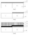
- Figures 4 to 6 represent schematically an alternative integration route for forming a gate stack of a semiconductor device comprising a first region and a second region in accordance with embodiments of the present invention.
- Various embodiments of the invention are referring to parameters of the semiconductor device such as threshold voltage, effective work function (eWF), or physical characteristics of the material(s) employed such as work function, Fermi level etc.
- eWF effective work function
- the substrate may include a semiconductor substrate such as e.g. a silicon, a gallium arsenide (GaAs), a gallium arsenide phosphide (GaAsP), an indium phosphide (InP), a germanium (Ge) or a silicon germanium (SiGe) substrate.
- a semiconductor substrate such as e.g. a silicon, a gallium arsenide (GaAs), a gallium arsenide phosphide (GaAsP), an indium phosphide (InP), a germanium (Ge) or a silicon germanium (SiGe) substrate.
- the substrate may include for example an insulating layer such as a SiO 2 or a Si 3 N 4 layer in addition to a substrate portion.
- the term substrate also includes silicon-on-glass, silicon-on-sapphire substrates.
- the term substrate is thus used to define generally the elements for layers that underlie a layer or portion(s) of interest.
- the substrate may be any other base on which a layer is formed, for example a glass or metal layer. Accordingly a substrate may be a wafer such as a blanket wafer or may be a layer applied to another base material, e.g. an epitaxial layer grown onto a lower layer.
- Some embodiments are suitable for integration into CMOS processing to provide CMOS devices.
- active regions can be formed by doping a semiconductor layer.
- An active region is defined as any region which becomes active due to the implantation of a dopant such as As, B, Ph, Sb, etc. In a MOS device this active region is often referred to as source and/or drain region.
- a dopant such as As, B, Ph, Sb, etc.
- this active region is often referred to as source and/or drain region.
- certain inventive aspects are not limited thereto.
- a MOSFET device comprises a first and second main electrode, e.g. source and drain electrode, at first and second extremities of a channel, and a control electrode, e.g. a gate electrode, for controlling the conductivity of the channel.
- a threshold voltage Vt
- Complementary MOS processes fabricate both n-channel and p-channel (NMOS and PMOS) transistors.
- the threshold voltage is influenced by what is called the effective work function difference.
- Vt threshold voltage
- the effective work function differences of the respective PMOS and NMOS gate materials (gate stacks) and their corresponding channel regions are independently established through channel processing and gate processing.
- both gate dielectric consisting e.g. of a host dielectric and different capping layers
- gate electrode consisting i.e. of at least one metal layer
- the gate processing itself i.e. the sequence of the different steps and/or the thermal treatments applied
- the effective work function of a gate stack is a parameter that can be tuned by the choice of the gate dielectric materials, gate electrode materials and by the gate processing performed.
- the work function of the gate electrode (often referred to as metal gate electrode or metal layer) is an intrinsic property of the material.
- the work function of a certain material e.g. a metal layer
- eV electron volts
- the gate electrode of a negative channel MOSFET (or NMOS) device would have an n-type work function of approximately 4.1 eV (+/-0.3 eV), and the gate electrode of a positive channel MOSFET (or PMOS) device would have a p-type work function of approximately 5.2 eV (+/-0.3 eV).
- the material may include non-stoichiometric variations of the stoichiometrically exact formula identified by the chemical name. Lack of numerical subscript by an element in the formula stoichiometrically signifies the number one. Variations in the range plus/minus 20% of the exact stoichiometric number are comprised in the chemical name or formula, for the purposes of the present invention. Where an algebraic subscript is given, then variations in the range plus/minus 20% relative to the value of each subscript are considered to form embodiments of the present invention. Such varied values do not necessarily sum to a whole number and this departure is contemplated. Such variations may occur due to either intended selection and control of the process conditions, or due to unintended process variations.
- the present invention provides a method for manufacturing a dual work function semiconductor device.
- the method comprises providing a substrate 5, and defining at least a first region I and a second region II in said substrate 5, the first region I being different from the second region II.
- the substrate may be any type of substrate as described above. With first region I is meant at least part of the substrate 5. With second region II is meant at least another part of the substrate 5.
- the first region I and the second region II are distinct regions. There is no overlap between the first region I and the second region II.
- the first region I and the second region II may be separated using isolation between said first and second region (not illustrated in the drawings), such as for example shallow trench isolation (STI) zones or local oxidation of silicon (LOCOS) zones. Alternatively, mesa isolation may be used as for example in the case when a silicon-on-insulator (SOI) substrate is used.
- STI shallow trench isolation
- LOC local oxidation of silicon
- the method comprises forming a first control electrode stack, e.g. gate stack, on the first region I, the first control electrode stack having a first effective work function, and forming a second control electrode stack, e.g. gate stack, on the second region II, the second control electrode stack having a second effective work function, each control electrode stack comprising a control electrode dielectric 1, 3; 1, 2, 3 and a control electrode 4, e.g. a metal control electrode.
- Forming the control electrode stacks, i.e. forming the control electrode dielectrics 1, 3; 1, 2, 3 and the control electrodes 4 may comprises some or all of the following steps:
- a method according to embodiments of the present invention improves leakage performance of dual workfunction semiconductor devices, due to the healing (repair) effect of the Hf-based dielectric capping layer 3 on the exposed surface of the host dielectric 1, previously damaged by the selective removal step, e.g. a selective etch step of the first dielectric capping layer 1 (surface defects by the removal of the first dielectric capping layer 1, dangling bonds).
- the Hf-based dielectric capping layer 3 has essentially no influence on the effective work function of the first and second control electrode stacks.
- An advantage of the method according to embodiments of the present invention is that the Hf-based dielectric capping layer 3 does not have to be selectively removed from the first capping layer 2 or from the host dielectric layer 1 on one of the regions. This reduces damage of the underlying layers, hence deterioration of the device, e.g. leakage.
- first dielectric capping layer 2 It is particularly difficult to find a dielectric material suitable as first dielectric capping layer 2 (having a high k-value and the right contribution on the effective work function tuning) and, at the same time, showing enough selectivity towards another dielectric material (host dielectric 1) and towards a photoresist mask material as used in standard semiconductor layer removal processes, e.g. wet chemical solutions.
- the first region I is an NMOS region and the second region II is a PMOS region.
- the first dielectric capping layer 2 may be an Al-based dielectric.
- the first dielectric capping layer 2 may consist of aluminum oxide (AlO x , with 0 ⁇ x ⁇ 2).
- the first region I is a PMOS region and the second region II is an NMOS region.
- the first dielectric capping layer 2 may be a lanthanide-based dielectric or an Sc-based dielectric.
- the first dielectric capping layer 2 may be a dielectric selected from the group comprising or consisting of D y O x , LaO x , ScO x (with 0 ⁇ x ⁇ 2) and mixtures thereof.
- the Hf-based dielectric capping layer 3 consists of HfLaO.
- the thickness of the Hf-based dielectric capping layer 3 is about 1 to 10 cycles ALD (Atomic Layer Deposition).
- ALD Atomic Layer Deposition
- the method according to embodiments of the present invention has the additional advantage that a dual work function device can be manufactured with a minor EOT (equivalent oxide thickness) increase, due to the very thin capping layers 3 employed.
- the host dielectric layer 1 may be selected from the group comprising or consisting of SiO 2 , SiON, HfO 2 , ZrO 2 and mixtures thereof.
- the control electrode dielectric 1, 2, 3 may further comprise an interfacial layer (not illustrated in the drawings), in contact with the semiconductor substrate 5 and underlying the host dielectric layer 1.
- Such interfacial layer may be formed as a result of an optional pre-cleaning process step, prior to forming the host dielectric layer 1.
- this interfacial layer may consist of an oxide of the semiconductor material of the substrate 5 (e.g. SiO 2 ).
- the interfacial layer may have a thickness lower than 0.7 nm, preferably lower than 0.4 nm.
- Selecting SiO 2 , SiON, HfO 2 , ZrO 2 or combinations thereof as host dielectric layer 1 and a Hf-based dielectric (in particular for example HfLaO) as a second dielectric capping layer 3 has the additional advantage of minimizing the impact of a change of used dielectric material; which change of material is generally known to often require expensive adaptations in a manufacturing flow (dedication of tools, expensive/hazardous precursors, etc.) .
- the integration route chosen matches the classic (existing) integration routes, mostly using a SiON dielectric as a host dielectric in contact with the substrate.
- control electrode 4 can be a metal electrode made of at least one layer of metal or a FUSI (Fully silicided) electrode.
- a method for manufacturing a dual work function semiconductor device comprises providing a substrate 5 with a first region I and a second region II, forming a first control electrode stack, e.g. gate stack, on the first region I, the first control electrode stack having a first effective work function, and forming a second control electrode stack, e.g. gate stack, on the second region II, the second control electrode stack having a second effective work function, each control electrode stack comprising a control electrode dielectric 3; 1, 2, 3 and a control electrode 4, e.g. a metal control electrode.
- the process of forming the control electrode stacks on the first region I and the second region II, the control electrode stacks comprising control electrode dielectric 3; 1, 2, 3 and the control electrode 4 comprises at least:
- an alternative integration route is disclosed, wherein both the host dielectric layer 1 and the first dielectric capping layer 2 are removed selectively towards the substrate 5 on the first region I.
- This alternative integration route presents the advantage of avoiding a selective removal step, e.g. a selective etch, of the first dielectric capping layer 2 stopping on the host dielectric layer 1. Selectivity concerns, e.g. with regard to etching an AIO layer 2 stopping on a SiON layer 1, are in this way avoided.
- both the first dielectric capping layer 2 and the host dielectric layer 1 are removed on the first region I, the removal stopping on the substrate 5.
- the Hf-based dielectric layer 3 deposited in this alternative integration route may be thicker than 1-10 cycles ALD.
- the thickness of the Hf-based dielectric layer 3 may for example range between about 1-2 nm, since the Hf-based dielectric layer 3 will act as a main dielectric layer (in contact with the substrate 5) on the first region I.
- the Hf-based dielectric layer 3 may comprise another Hfbased material such as HfO2 or HfSiON.
- the first dielectric capping layer 2 may in this alternative integration route be thinner that in the previous embodiment in order to keep the EOT value of the control electrode dielectric stack essentially unchanged.
- a dual work function semiconductor device comprising a first transistor on a first substrate region I, the first transistor having a first effective work function, and a second transistor on a second substrate region II, the second transistor having a second effective work function.
- the first transistor comprises a host dielectric layer 1 overlying and in contact with a substrate 5, a control electrode 4, e.g. a metal control electrode 4, and a Hf-based dielectric capping layer 3 sandwiched in between the host dielectric layer 1 and the control electrode 4.
- the second transistor comprises a host dielectric layer 1 overlying and in contact with the substrate 5, a control electrode 4, e.g. a metal control electrode 4, a first dielectric capping layer 2 overlying the host dielectric layer 1, and a Hf-based dielectric capping layer 3 sandwiched in between the first dielectric capping layer 2 and the control electrode 4, e.g. metal control electrode, whereby the first dielectric capping layer 2 is selected to determine the second effective work function.
- the host dielectric layer 1 of the first transistor has substantially the same composition and same thickness as the host dielectric layer 1 of the second transistor.
- the control electrode 4 of the first transistor has substantially the same composition and same thickness as the control electrode 4 of the second transistor.
- the Hf-based dielectric capping layer 3 of the first transistor has substantially the same composition and same thickness as the Hf-based dielectric capping layer 3 of the second transistor.
- a Hf-based dielectric capping layer 3 sandwiched in between the host dielectric layer 1 and the control electrode 4" used herein refers to a Hf-based dielectric capping layer 3 overlying and in contact with the host dielectric layer 1 and underlying and in contact with the control electrode 4.
- a Hf-based dielectric capping layer 3 sandwiched in between the first dielectric capping layer 2 and the control electrode 4" refers to a Hf-based dielectric capping layer 3 overlying and in contact with the first dielectric capping layer 2 and underlying and in contact with the control electrode 1.
- the first region I is an NMOS region and the second region II is a PMOS region.
- the first dielectric capping layer 2 may be an Al-based dielectric.
- the first dielectric capping layer 2 may consists of aluminum oxide (AlOx, with 0 ⁇ x ⁇ 2).
- the first region I is a PMOS region and the second region II is an NMOS region.
- the first dielectric capping layer 2 may be a lanthanide-based dielectric or an Sc-based dielectric.
- the first dielectric capping layer 2 may be a dielectric selected from the group comprising or consisting of DyOx, LaOx, ScOx (with 0 ⁇ x ⁇ 2) and mixtures thereof.
- the thickness of the Hf-based dielectric 3 is from about 1 to 10 cycles ALD.
- the Hf-based dielectric 3 consists of HfLaO.
- the first transistor comprises a control electrode 4, e.g. a metal control electrode 4, and a Hf-based dielectric capping layer 3 sandwiched in between a substrate 5 and the control electrode 4.
- the second transistor comprises a host dielectric layer 1 overlying and in contact with the substrate 5, a control electrode 4, e.g. a metal control electrode 4, a first dielectric capping layer 2 overlying the host dielectric layer 1, and a Hf-based dielectric capping layer 3 sandwiched in between the first dielectric capping layer 2 and the control electrode 4, e.g. metal control electrode, whereby the first dielectric capping layer 2 is selected to determine the second effective work function.
- control electrode 4 of the first transistor has substantially the same composition and same thickness as the control electrode 4 of the second transistor.
- the Hf-based dielectric capping layer 3 of the first transistor has substantially the same composition and same thickness as the Hf-based dielectric capping layer 3 of the second transistor.
- a Hf-based dielectric capping layer 3 sandwiched in between a substrate 5 and the control electrode 4" used herein refers to a Hf-based dielectric capping layer 3 overlying and in contact with the substrate 5 and underlying and in contact with the control electrode 4.
- a Hf-based dielectric capping layer 3 sandwiched in between the first dielectric capping layer 2 and the control electrode 4" refers to a Hf-based dielectric capping layer 3 overlying and in contact with the first dielectric capping layer 2 and underlying and in contact with the control electrode 1.
- the thickness of the Hf-based dielectric 3 may for example range between about 1-2 nm.
- the Hf-based dielectric 3 may consist of HfLaO.
- the Hf-based dielectric layer 3 may comprise a Hf-based dielectric material such as HfLaO, or another Hf-based material such as HfO 2 or HfSiON, or combinations of one or more of these materials.
Landscapes
- Metal-Oxide And Bipolar Metal-Oxide Semiconductor Integrated Circuits (AREA)
- Electrodes Of Semiconductors (AREA)
- Formation Of Insulating Films (AREA)
Abstract
providing a substrate (5) with a first region (I) and a second region (II);
forming a first control electrode stack on the first region (I), the first control electrode stack having a first effective work function, and forming a second control electrode stack on the second region (II), the second control electrode stack having a second effective work function, wherein each control electrode stack comprises a control electrode dielectric and a control electrode. The process of forming the control electrode stacks comprises:
(i) forming a host dielectric layer (1) overlying the first region (I) and the second region (II) of the substrate (5),
(ii) forming a first dielectric capping layer (2) overlying the host dielectric layer (1) on the first region (I) and on the second region (II), wherein the first dielectric capping layer is selected to determine the second effective work function,
(iii) removing at least the first dielectric capping layer (1) selectively to an underlying layer (1; 5) on the first region (I), thereby exposing the underlying layer (1; 5) on the first region (I),
(iv) forming a Hf-based dielectric capping layer (3) overlying the underlying layer (1; 5) on the first region and the first dielectric capping layer (2) on the second region (II), wherein the Hf-based dielectric capping layer (3) is selected to have a healing effect on the exposed surface of the underlying layer (1; 5) on the first region (I), and
(v) forming a control electrode (4) overlaying the Hf-based dielectric capping layer (3) on the first region (I) and on the second region (II).
Description
- The present invention generally relates to semiconductor devices. More specifically, this invention relates to fabrication of semiconductor devices comprising semiconductor structures comprising a single control electrode and different dielectric materials. In particular, the present invention relates to methods for manufacturing dual work function semiconductor devices and to dual work function semiconductor devices thus obtained. Particularly, the invention may relate to dual work function devices comprising a single metal control electrode and a control electrode dielectric comprising dielectric capping layers. For example, the present invention may relate to complementary metal oxide semiconductor (CMOS) devices.
- Up to now, semiconductor industry remains driven by scaling geometric dimensions of metal-oxide-semiconductor field-effect-transistors (MOSFETs). With traditional MOSFET technology, using silicon dioxide (SiO2) as gate dielectric and polycrystalline silicon (poly-Si) as gate material, a lot of problems occur when scaling down to 100 nm or below.
- Scaling MOSFETs to improve performance results leads to higher gate leakage as the gate dielectric, e.g. SiO2 gate dielectric, becomes thinner. To address this issue, SiO2 gate dielectrics have been replaced with high-k materials (e.g. Hf-based or Al-based material with a k-value larger than the k-value of SiO2, also called high-k materials, i.e. with a k-value above 3.9). High-k dielectrics allow for a larger physical thickness (compared to SiO2) for obtaining a same effective capacitance than can be obtained with a much thinner SiO2 layer. The larger physical thickness of the high-k material will reduce gate leakage currents. With the introduction of the high-k materials, however, a new problem arose, namely the Fermi level pinning effect. Fermi level pinning is a fundamental characteristic of the semiconductor, e.g. polysilicon (polySi)/oxide interface that causes high threshold voltages in MOSFET devices.
- A known solution to this problem is the introduction of metal gates. However, it has been proven difficult to identify band-edge metals (metals with either a n-type or a p-type work function (WF), required for low device voltage threshold, Vt) that are compatible with the conventional CMOS fabrication process. CMOS can be made using dual metal gates with single or dual dielectrics. In either case, a selective removal of one of the metal gates is necessary and adds substantial complexity and costs to the manufacturing process. Moreover, after the selective removal process, the interface between the underlying dielectric layer and the metal electrode is often modified/ altered, due to the presence of undesired dangling bonds. This modification may influence the effective work function of the gate stack in an unwanted way.
- Another known solution for CMOS manufacturing is to use FUlly Sllicided (FUSI) gates, without a selective removal of electrode or gate dielectric. However, to obtain appreciate WF, FUSI gates require different silicide phases on nMOS and pMOS. On small devices, the phase or composition of the FUSI gate tends to distribute unevenly, resulting in severe within-wafer threshold voltage (Vt) non-uniformity.
- It is an object of embodiments of the present invention to alleviate or overcome problems and disadvantages of the prior art methods and devices.
- The above objective is accomplished by a method and device according to the present invention.
- In one aspect, the present invention provides a method for manufacturing a dual work function semiconductor device. The method comprises:
- providing a substrate with a first region and a second region;
- forming a first control electrode stack on the first region, the first control electrode stack having a first effective work function and forming a second control electrode stack on the second region, the second control electrode stack having a second effective work function, wherein each control electrode stack comprises a control electrode dielectric and a control electrode. According to the present invention, the process of forming the control electrode stacks comprises:
- (i) forming a host dielectric layer overlying the first region and the second region of the substrate,
- (ii) forming a first dielectric capping layer overlying the host dielectric layer on the first region and on the second region, wherein the first dielectric capping layer is selected to determine the second effective work function,
- (iii) removing at least the first dielectric capping layer selectively to an underlying layer on the first region, thereby exposing the underlying layer on the first region,
- (iv) forming a Hf-based dielectric capping layer overlying the underlying layer on the first region and the first dielectric capping layer on the second region, wherein the Hf-based dielectric capping layer is selected to have a healing effect on the exposed surface of the underlying layer on the first region, and
- (v) forming a control electrode overlaying the Hf-based dielectric capping layer on the first region and on the second region.
- It is an advantage of embodiments of the present invention that, due to the healing effect of the Hf-based dielectric capping layer on the underlying layer, leakage performance of realised devices is improved.
- It is a further advantage of embodiments of the present invention that the Hf-based dielectric capping layer does not need to be removed when further processing dual work function devices.
- In embodiments of the present invention, the underlying layer is the host dielectric layer. In alternative embodiments, the underlying layer is the substrate. Both embodiments define different integration routes for the manufacturing methods according to embodiments of the present invention.
- In embodiments of the present invention, the first and second region are of different, e.g. opposite, dopant type. In embodiments of the present invention, the first region may be an NMOS region and the second region may be a PMOS region. In this case, the first dielectric capping layer may for example be an Al-based dielectric. In alternative embodiments of the present invention, the first region may be a PMOS region and the second region may be an NMOS region.
- In this case the first dielectric capping layer may for example be a lanthanide-based dielectric or an Sc-based dielectric.
- In embodiments of the present invention, forming the Hf-based dielectric capping layer may comprise depositing the Hf-based dielectric capping layer, for example by ALD. Depositing the Hf-based dielectric capping layer by ALD may comprise depositing during 1 to 10 cycles ALD.
- In embodiments of the present invention, the Hf-based dielectric capping layer may comprise HfLaO. In particular embodiments, the Hf-based dielectric capping layer may consist of HfLaO.
- In embodiments of the present invention, the host dielectric layer may be selected from the group consisting of Si02, SiON, Hf02, Zr02 and mixtures thereof.
- In embodiments of the present invention, forming a control electrode may comprise forming a first control electrode in the first region, and forming a second control electrode in the second region. The first electrode and the second electrode may be formed of a same layer of electrode material. Therefore, the first electrode and the second electrode may have the same thickness and material composition. In embodiments of the present invention, forming a control electrode may comprise forming a metal control electrode.
- In another aspect, the present invention provides a dual work function semiconductor device, comprising a first transistor on a first region of a substrate, the first transistor having a first effective work function, and a second transistor on a second region of the substrate, the second transistor having a second effective work function. The first transistor comprises an underlying layer, a control electrode and a Hf-based dielectric capping layer sandwiched in between the underlying layer and the control electrode. The second transistor comprises a host dielectric layer overlying and in contact with the substrate, a control electrode, a first dielectric capping layer overlying the host dielectric layer and a Hf-based dielectric capping layer sandwiched in between the first dielectric capping layer and the control electrode, whereby the first dielectric capping layer is selected to determine the second effective work function. The control electrode of the first transistor has substantially the same composition and same thickness as the control electrode of the second transistor, and the Hf-based dielectric capping layer of the first transistor has substantially the same composition and same thickness as the Hf-based dielectric capping layer of the second transistor.
- In embodiments of the present invention, the underlying layer may be the host dielectric layer. It is an advantage of such embodiments of the present invention that a same dielectric material, also referred to as host dielectric material, is used for different semiconductor structures of a semiconductor device. Since one host dielectric material is used for the different semiconductor structures, the process comes close to well-known conventional CMOS processes and gives better control of the integrity performance of the control electrode dielectric material.
- In alternative embodiments, the underlying layer may be the substrate.
- In embodiments of the present invention, the control electrode may be made from a metal comprising material. The metal comprising material may comprise any of a metal, a metal alloy, a metal silicide, a conductive metal nitride or a conductive metal oxide. Said electrode material may comprise Ta, Hf, Mo, W or Ru. In alternative embodiments said electrode material may also be polysilicon. In yet alternative embodiments, said first and/or second electrode may be a silicided electrode. Said silicided first and/or second electrode are preferably fully silicided.
- In embodiments of the present invention, the first region and the second region may be of different, e.g. opposite, dopant types. In particular embodiments, the first region may be an NMOS region and the second region may be a PMOS region. In such embodiments, the first dielectric capping layer may for example be an Al-based dielectric. In alternative particular embodiments, the first region may be a PMOS region and the second region may be an NMOS region. In such embodiments, the first dielectric capping layer may for example be a lanthanide-based dielectric or an Sc-based dielectric.
- In embodiments of the present invention, the thickness of the Hf-based dielectric layer may be 1 to 10 cycles ALD. In alternative embodiments, the thickness of the Hf-based dielectric layer may be between 1 and 2 nm.
- In embodiments of the present invention, the Hf-based dielectric layer may comprise HfLaO. In particular embodiments it may consist of HfLaO.
- In embodiments of the present invention, the host dielectric layer may be selected from the group consisting of Si02, SiON, Hf02, Zr02 and mixtures thereof.
- Particular and preferred aspects of the invention are set out in the accompanying independent and dependent claims. Features from the dependent claims may be combined with features of the independent claims and with features of other dependent claims as appropriate and not merely as explicitly set out in the claims.
- The above and other characteristics, features and advantages of the present invention will become apparent from the following detailed description, taken in conjunction with the accompanying drawings, which illustrate, by way of example, the principles of the invention. This description is given for the sake of example only, without limiting the scope of the invention. The reference figures quoted below refer to the attached drawings.
- All drawings are intended to illustrate some aspects and embodiments of the present invention. The drawings described are only schematic and are nonlimiting.
-
Figures 1 to 3 represent schematically an integration route for forming a gate stack of a semiconductor device comprising a first region and a second region in accordance with embodiments of the present invention. -
Figures 4 to 6 represent schematically an alternative integration route for forming a gate stack of a semiconductor device comprising a first region and a second region in accordance with embodiments of the present invention. - In the different figures, the same reference signs refer to the same or analogous elements.
- The present invention will be described with respect to particular embodiments and with reference to certain drawings but the invention is not limited thereto but only by the claims. The drawings described are only schematic and are nonlimiting. In the drawings, the size of some of the elements may be exaggerated and not drawn on scale for illustrative purposes. The dimensions and the relative dimensions do not correspond to actual reductions to practice of the invention.
- Furthermore, the terms first, second, third and the like in the description and in the claims, are used for distinguishing between similar elements and not necessarily for describing a sequence, either temporally, spatially, in ranking or in any other manner. It is to be understood that the terms so used are interchangeable under appropriate circumstances and that the embodiments of the invention described herein are capable of operation in other sequences than described or illustrated herein.
- Moreover, the terms top, bottom, over, under and the like in the description and the claims are used for descriptive purposes and not necessarily for describing relative positions. It is to be understood that the terms so used are interchangeable under appropriate circumstances and that the embodiments of the invention described herein are capable of operation in other orientations than described or illustrated herein.
- It is to be noticed that the term "comprising", used in the claims, should not be interpreted as being restricted to the means listed thereafter; it does not exclude other elements or steps. It is thus to be interpreted as specifying the presence of the stated features, integers, steps or components as referred to, but does not preclude the presence or addition of one or more other features, integers, steps or components, or groups thereof. Thus, the scope of the expression "a device comprising means A and B" should not be limited to devices consisting only of components A and B. It means that with respect to the present invention, the only relevant components of the device are A and B.
- All numbers expressing thicknesses and so forth used in the specification and claims are to be understood as being modified in all instances by the term "about". Accordingly, unless indicated to the contrary, the numerical parameters set forth in the specification and attached claims are approximations that may vary depending upon the desired properties sought to be obtained by the present invention. At the very least, each numerical parameter should be construed in light of the number of significant digits and ordinary rounding approaches.
- Reference throughout this specification to "one embodiment" or "an embodiment" means that a particular feature, structure or characteristic described in connection with the embodiment is included in at least one embodiment of the present invention. Thus, appearances of the phrases "in one embodiment" or "in an embodiment" in various places throughout this specification are not necessarily all referring to the same embodiment, but may. Furthermore, the particular features, structures or characteristics may be combined in any suitable manner, as would be apparent to one of ordinary skill in the art from this disclosure, in one or more embodiments.
- Similarly it should be appreciated that in the description of exemplary embodiments of the invention, various features of the invention are sometimes grouped together in a single embodiment, figure, or description thereof for the purpose of streamlining the disclosure and aiding in the understanding of one or more of the various inventive aspects. This method of disclosure, however, is not to be interpreted as reflecting an intention that the claimed invention requires more features than are expressly recited in each claim. Rather, as the following claims reflect, inventive aspects lie in less than all features of a single foregoing embodiment of the present invention. Thus, the claims following the detailed description are hereby expressly incorporated into this detailed description, with each claim standing on its own as a separate embodiment of this invention.
- Furthermore, while some embodiments described herein include some but not other features included in other embodiments, combinations of features of different embodiments are meant to be within the scope of the invention, and form different embodiments, as would be understood by those in the art. For example, in the following claims, any of the claimed embodiments can be used in any combination.
- In the description provided herein, numerous specific details are set forth. However, it is understood that embodiments of the invention may be practiced without these specific details. In other instances, well-known methods, structures and techniques have not been shown in detail in order not to obscure an understanding of this description.
- Various embodiments of the invention are referring to parameters of the semiconductor device such as threshold voltage, effective work function (eWF), or physical characteristics of the material(s) employed such as work function, Fermi level etc. The definitions as used through this document are summarized herein-below.
- In the following, certain embodiments will be described with reference to device structures such as field effect transistors having two main electrodes and a control electrode, but the inventive aspect is not limited thereto. In the following, certain embodiments will also be described with reference to a silicon substrate but is should be understood that certain inventive aspects apply equally well to other semiconductor substrates. In embodiments, the substrate may include a semiconductor substrate such as e.g. a silicon, a gallium arsenide (GaAs), a gallium arsenide phosphide (GaAsP), an indium phosphide (InP), a germanium (Ge) or a silicon germanium (SiGe) substrate. The substrate may include for example an insulating layer such as a SiO2 or a Si3N4 layer in addition to a substrate portion. Thus, the term substrate also includes silicon-on-glass, silicon-on-sapphire substrates. The term substrate is thus used to define generally the elements for layers that underlie a layer or portion(s) of interest. Also, the substrate may be any other base on which a layer is formed, for example a glass or metal layer. Accordingly a substrate may be a wafer such as a blanket wafer or may be a layer applied to another base material, e.g. an epitaxial layer grown onto a lower layer.
- Some embodiments are suitable for integration into CMOS processing to provide CMOS devices. In such processing active regions can be formed by doping a semiconductor layer. An active region is defined as any region which becomes active due to the implantation of a dopant such as As, B, Ph, Sb, etc. In a MOS device this active region is often referred to as source and/or drain region. However, certain inventive aspects are not limited thereto.
- A MOSFET device comprises a first and second main electrode, e.g. source and drain electrode, at first and second extremities of a channel, and a control electrode, e.g. a gate electrode, for controlling the conductivity of the channel. When using a MOSFET device, a threshold voltage (Vt) needs to be applied to the gate to render the channel conductive. Complementary MOS processes fabricate both n-channel and p-channel (NMOS and PMOS) transistors. The threshold voltage is influenced by what is called the effective work function difference. To establish threshold voltage (Vt) values, the effective work function differences of the respective PMOS and NMOS gate materials (gate stacks) and their corresponding channel regions are independently established through channel processing and gate processing. In other words, both gate dielectric (consisting e.g. of a host dielectric and different capping layers) and gate electrode (consisting i.e. of at least one metal layer) determine the effective work function of the gate stack (device). Moreover, the gate processing itself (i.e. the sequence of the different steps and/or the thermal treatments applied) may have an influence on the effective work function of the gate stack (device).
- The effective work function of a gate stack (device) is a parameter that can be tuned by the choice of the gate dielectric materials, gate electrode materials and by the gate processing performed. On the contrary, the work function of the gate electrode (often referred to as metal gate electrode or metal layer) is an intrinsic property of the material. In general, the work function of a certain material (e.g. a metal layer) is a measure of the energy, in electron volts (eV), required to eject an electron in the material outside of a material atom to the vacuum, if the electron were initially at the Fermi level.
- For a silicon substrate, the gate electrode of a negative channel MOSFET (or NMOS) device would have an n-type work function of approximately 4.1 eV (+/-0.3 eV), and the gate electrode of a positive channel MOSFET (or PMOS) device would have a p-type work function of approximately 5.2 eV (+/-0.3 eV).
- Where, herein, a specific chemical name or formula is given, the material may include non-stoichiometric variations of the stoichiometrically exact formula identified by the chemical name. Lack of numerical subscript by an element in the formula stoichiometrically signifies the number one. Variations in the range plus/minus 20% of the exact stoichiometric number are comprised in the chemical name or formula, for the purposes of the present invention. Where an algebraic subscript is given, then variations in the range plus/minus 20% relative to the value of each subscript are considered to form embodiments of the present invention. Such varied values do not necessarily sum to a whole number and this departure is contemplated. Such variations may occur due to either intended selection and control of the process conditions, or due to unintended process variations.
- The invention will now be described by a detailed description of several embodiments of the invention. It is clear that other embodiments of the invention can be configured according to the knowledge of persons skilled in the art without departing from the technical teaching of the invention as defined by the appended claims.
- In a first aspect, the present invention provides a method for manufacturing a dual work function semiconductor device.
- In a first embodiment of the first aspect, illustrated in
Figures 1, 2 and 3 , the method comprises providing asubstrate 5, and defining at least a first region I and a second region II in saidsubstrate 5, the first region I being different from the second region II. The substrate may be any type of substrate as described above. With first region I is meant at least part of thesubstrate 5. With second region II is meant at least another part of thesubstrate 5. The first region I and the second region II are distinct regions. There is no overlap between the first region I and the second region II. The first region I and the second region II may be separated using isolation between said first and second region (not illustrated in the drawings), such as for example shallow trench isolation (STI) zones or local oxidation of silicon (LOCOS) zones. Alternatively, mesa isolation may be used as for example in the case when a silicon-on-insulator (SOI) substrate is used. - The method comprises forming a first control electrode stack, e.g. gate stack, on the first region I, the first control electrode stack having a first effective work function, and forming a second control electrode stack, e.g. gate stack, on the second region II, the second control electrode stack having a second effective work function, each control electrode stack comprising a
control electrode dielectric control electrode 4, e.g. a metal control electrode. Forming the control electrode stacks, i.e. forming thecontrol electrode dielectrics control electrodes 4 may comprises some or all of the following steps: - (i) Optionally, in a first step the surface of the
substrate 5 may be pre-cleaned with standard cleaning techniques, such as for example RCA clean, to remove any organic contaminants or native oxide on the wafer substrate or semiconductor substrate. - (ii) Forming a
host dielectric layer 1 overlying both the first region I and the second region II of thesubstrate 5, as illustrated inFigure 1 . Saidhost dielectric layer 1 may cover thewhole substrate 5 or only parts thereof. With host dielectric material is meant that the dielectric material is used for the main purpose as a control electrode dielectric, e.g. gate dielectric, in a semiconductor device, namely as a dielectric barrier between the control electrode, e.g. gate electrode, and a channel region of the semiconductor structures forming the semiconductor device. In embodiments of the present invention, thehost dielectric layer 1 is selected from the group consisting of SiO2, SiON, HfO2, ZrO2 and mixtures thereof. Thehost dielectric layer 1 may be deposited by chemical-vapor-deposition (CVD) techniques. Most commonly used are metal organic CVD (MOCVD) and atomic layer deposition (ALD). Alternatively, saidhost dielectric layer 1 maybe deposited with other suitable deposition techniques known to a person skilled in the art. - (iii) Optionally, to improve the electrical characteristics of the
host dielectric layer 1, post-deposition annealing (PDA) may be performed. - (iv) In a next step, a first
dielectric capping layer 2 is formed overlying thehost dielectric layer 1 on the first region I and on the second region II, as illustrated inFigure 1 , wherein the firstdielectric capping layer 2 is selected to determine, in co-operation with thehost dielectric layer 1, the effective work function of the second control electrode stack. Said firstdielectric capping layer 2 is on and in contact with said underlyinghost dielectric layer 1. With 'in contact with' is meant that the firstdielectric capping layer 2 is in direct contact with thehost dielectric layer 1 which is positioned in between thesubstrate 5 and the firstdielectric capping layer 2. Said firstdielectric capping layer 2 may be provided by any suitable method, such as deposition techniques, for example CVD, ALD or PVD techniques. Alternatively, said firstdielectric capping layer 2 may be deposited with other suitable low temperature deposition techniques known to a person skilled in the art. According to embodiments of the present invention the firstdielectric capping layer 2 may comprise a dielectric material which can tune the work function of a control electrode stack formed by completing subsequent steps. In embodiments of the present invention, said dielectric material may be an Al-based dielectric, for example AlOx, with 0<x<2. In alternative embodiments, the dielectric material may be a lanthanide-based or an Sc-based dielectric. The dielectric may for example be a dielectric selected from the group consisting of DyOx, LaOx or ScOx (with 0<x<2) and mixtures thereof. - (v) Thereafter, at least the first
dielectric capping layer 2 is patterned so that the firstdielectric capping layer 2 is selectively removed at least on the first region I, the selectivity of the removal of the first dielectric capping layer being towards to thehost dielectric layer 1, thereby exposing thehost dielectric layer 1 on the first region I, as illustrated inFigure 2 . The patterning is such that the firstdielectric capping layer 2 remains on and in contact with thehost dielectric layer 1 on the second region II. For patterning the firstdielectric capping layer 2, a masking material (not illustrated) may be deposited on said firstdielectric capping layer 2, such as for example resist, followed by a lithographic step. This lithographic step may comprise exposing the resist using a mask, followed by patterning the exposed region such that the exposed zone, e.g. the zone above the first region I, is removed. Alternatively, and depending on the kind of lithography used, the zone above the second region II may be exposed and the unexposed part of the resist, i.e. the resist above the first region I, may be removed. After said lithographic step, said firstdielectric capping layer 2 may be removed, e.g. etched using a dry or wet etching technique depending on the material of the firstdielectric capping layer 2. - (vi) In a next step, a Hf-based
dielectric capping layer 3 is formed overlying thehost dielectric layer 1 on the first region I and the firstdielectric capping layer 2 on the second region II, as illustrated inFigure 3 , wherein the Hf-baseddielectric capping layer 3 is selected to have a healing effect on the exposed surface of thehost dielectric layer 1 on the first region I. Healing is the repair of the exposed surface of thehost dielectric layer 1 which is damaged by the removal step, e.g. selective etch step, of the firstdielectric capping layer 2. The damage comprises surface defects and dangling bonds originating from the interaction between the etch chemicals and thehost dielectric layer 1, which act as interface traps and affect the electrical performance of the device. Providing the Hf-baseddielectric capping layer 3 saturates the previously generated defects. The Hf-baseddielectric capping layer 3 should be conformal with a good uniformity in thickness and composition over the substrate. The conformality is an intrinsic characteristic of ALD, good uniformity can be achieved. Furthermore, the Hf-baseddielectric capping layer 3 should have a stable interface with the control electrode, e.g. no intermixing, good adhesion. In embodiments wherein the layer underlying the Hf-basedcapping layer 3 is thehost dielectric layer 1, the Hf-baseddielectric capping layer 3 should be thin (1-10 cycle ALD) with a minor contribution to EOT. In alternative embodiments wherein the layer underlying the Hf-baseddielectric capping layer 3 is thesubstrate 5, the Hf-baseddielectric capping layer 3 should have a good quality interface with the substrate 5 (e.g. no defects) and should have a good uniformity in thickness and composition over thesubstrate 5. In these embodiments the Hf-baseddielectric capping layer 3 will later on form the control electrode dielectric, e.g. gate dielectric, on the first region I. - (vii) In a next step a
control electrode 4 is formed overlaying the Hf-baseddielectric capping layer 3 on the first region I and on the second region II, as illustrated inFigure 3 . A first control electrode may be formed on the first region I, and a second control electrode may be formed on the second region II. According to embodiments of the present invention, the first electrode may be the same as the second electrode, or in other words the first and second electrode may be formed of a same layer of electrode material, as illustrated inFigure 3 . Said first and/or second electrode material may comprise a metal comprising material to form a metal gate. With metal comprising material is understood metals, metal alloys, metal silicides, conductive metal nitrides, conductive metal oxides, ... For example the metal comprising material may comprise Ta, Hr, Mo, W or Ru or may comprises Ta-based metals such as TaCxNy. Said electrode may alternatively comprise polysilicon or may be a fully silicided (FUSI) metal electrode. In FUSI technology, a thin polysilicon electrode is deposited as in a conventional CMOS process. Next a metal (e.g. nickel or hafnium) is then deposited and followed by rapid thermal annealing (RTA) to fully silicidise the electrode. - (viii) After depositing the
control electrode 4, further process steps may be performed as in conventional CMOS processing. Said process steps may comprise patterning the control electrode and the dielectric stack, implantation steps to form first and second main electrode regions, e.g. source and drain regions in said first region I and said second region II, formation of spacers aside the control electrodes, etc. - Advantageously, a method according to embodiments of the present invention improves leakage performance of dual workfunction semiconductor devices, due to the healing (repair) effect of the Hf-based
dielectric capping layer 3 on the exposed surface of thehost dielectric 1, previously damaged by the selective removal step, e.g. a selective etch step of the first dielectric capping layer 1 (surface defects by the removal of the firstdielectric capping layer 1, dangling bonds). More advantageously, the Hf-baseddielectric capping layer 3 has essentially no influence on the effective work function of the first and second control electrode stacks. - An advantage of the method according to embodiments of the present invention is that the Hf-based
dielectric capping layer 3 does not have to be selectively removed from thefirst capping layer 2 or from thehost dielectric layer 1 on one of the regions. This reduces damage of the underlying layers, hence deterioration of the device, e.g. leakage. - It is a further advantage of embodiments of the present invention that no sacrificial layers need to be applied in order to manufacture a dual workfunction semiconductor device in accordance with embodiments of the present invention. This makes the workflow easier.
- It is particularly difficult to find a dielectric material suitable as first dielectric capping layer 2 (having a high k-value and the right contribution on the effective work function tuning) and, at the same time, showing enough selectivity towards another dielectric material (host dielectric 1) and towards a photoresist mask material as used in standard semiconductor layer removal processes, e.g. wet chemical solutions.
- In one type of embodiments of the first aspect of the invention, the first region I is an NMOS region and the second region II is a PMOS region. Further in the same type of embodiments the first
dielectric capping layer 2 may be an Al-based dielectric. In particular embodiments, the firstdielectric capping layer 2 may consist of aluminum oxide (AlOx, with 0<x<2). - In another type of embodiments of the first aspect of the invention, the first region I is a PMOS region and the second region II is an NMOS region. In particular embodiments of this type of embodiments, the first
dielectric capping layer 2 may be a lanthanide-based dielectric or an Sc-based dielectric. In particular embodiments, the firstdielectric capping layer 2 may be a dielectric selected from the group comprising or consisting of DyOx, LaOx, ScOx (with 0<x<2) and mixtures thereof. - In some embodiments of the invention, the Hf-based
dielectric capping layer 3 consists of HfLaO. - In embodiments of the invention, the thickness of the Hf-based
dielectric capping layer 3 is about 1 to 10 cycles ALD (Atomic Layer Deposition). The method according to embodiments of the present invention has the additional advantage that a dual work function device can be manufactured with a minor EOT (equivalent oxide thickness) increase, due to the verythin capping layers 3 employed. - In embodiments of the invention, the
host dielectric layer 1 may be selected from the group comprising or consisting of SiO2, SiON, HfO2, ZrO2 and mixtures thereof. Thecontrol electrode dielectric semiconductor substrate 5 and underlying thehost dielectric layer 1. Such interfacial layer may be formed as a result of an optional pre-cleaning process step, prior to forming thehost dielectric layer 1. In embodiments of the present invention, this interfacial layer may consist of an oxide of the semiconductor material of the substrate 5 (e.g. SiO2). In embodiments of the present invention, the interfacial layer may have a thickness lower than 0.7 nm, preferably lower than 0.4 nm. - Selecting SiO2, SiON, HfO2, ZrO2 or combinations thereof as
host dielectric layer 1 and a Hf-based dielectric (in particular for example HfLaO) as a seconddielectric capping layer 3 has the additional advantage of minimizing the impact of a change of used dielectric material; which change of material is generally known to often require expensive adaptations in a manufacturing flow (dedication of tools, expensive/hazardous precursors, etc.) . In this way, the integration route chosen matches the classic (existing) integration routes, mostly using a SiON dielectric as a host dielectric in contact with the substrate. - In different embodiments of the invention the
control electrode 4 can be a metal electrode made of at least one layer of metal or a FUSI (Fully silicided) electrode. - In an alternative embodiment of the first aspect of the invention, illustrated in
Figures 4, 5 and 6 a method for manufacturing a dual work function semiconductor device is disclosed. The method comprises providing asubstrate 5 with a first region I and a second region II, forming a first control electrode stack, e.g. gate stack, on the first region I, the first control electrode stack having a first effective work function, and forming a second control electrode stack, e.g. gate stack, on the second region II, the second control electrode stack having a second effective work function, each control electrode stack comprising acontrol electrode dielectric 3; 1, 2, 3 and acontrol electrode 4, e.g. a metal control electrode. The process of forming the control electrode stacks on the first region I and the second region II, the control electrode stacks comprisingcontrol electrode dielectric 3; 1, 2, 3 and thecontrol electrode 4, comprises at least: - (i) forming a
host dielectric layer 1 overlying the first region I and the second region II of thesubstrate 5, as illustrated inFigure 4 , - (ii) forming a first
dielectric capping layer 2 overlying thehost dielectric layer 1 on the first region I and on the second region II, as illustrated inFigure 4 , wherein the firstdielectric capping layer 2 is selected to determine, in co-operation with thehost dielectric layer 1, the effective work function of the second control electrode stack, - (iii) removing the first
dielectric capping layer 2 and thehost dielectric layer 1 selectively to thesubstrate 5 on the first region I, thereby exposing thesubstrate 5 on the first region I, as illustrated inFigure 5 , - (iv) forming a Hf-based
dielectric capping layer 3 overlying thesubstrate 5 on the first region I and overlying the firstdielectric capping layer 2 on the second region II, as illustrated inFigure 6 , wherein the Hf-baseddielectric capping layer 3 is selected to have a healing effect on the exposed surface of thesubstrate 5 on the first region I, and - (v) forming a
control electrode 4 overlaying the Hf-baseddielectric capping layer 3 on the first region I and on the second region II, as illustrated inFigure 6 . - In this embodiment, an alternative integration route is disclosed, wherein both the
host dielectric layer 1 and the firstdielectric capping layer 2 are removed selectively towards thesubstrate 5 on the first region I. This alternative integration route presents the advantage of avoiding a selective removal step, e.g. a selective etch, of the firstdielectric capping layer 2 stopping on thehost dielectric layer 1. Selectivity concerns, e.g. with regard to etching anAIO layer 2 stopping on aSiON layer 1, are in this way avoided. In this embodiment both the firstdielectric capping layer 2 and thehost dielectric layer 1 are removed on the first region I, the removal stopping on thesubstrate 5. - Other process steps, material details, features of the layers, etc. as disclosed with respect to the first embodiment of the first aspect of the present invention, although not repeated here, also apply to this second embodiment of the first aspect of the present invention or can be combined therewith.
- The Hf-based
dielectric layer 3 deposited in this alternative integration route may be thicker than 1-10 cycles ALD. In embodiments of the present invention, the thickness of the Hf-baseddielectric layer 3 may for example range between about 1-2 nm, since the Hf-baseddielectric layer 3 will act as a main dielectric layer (in contact with the substrate 5) on the first region I. Alternatively, the Hf-baseddielectric layer 3 may comprise another Hfbased material such as HfO2 or HfSiON. - The first
dielectric capping layer 2 may in this alternative integration route be thinner that in the previous embodiment in order to keep the EOT value of the control electrode dielectric stack essentially unchanged. - In a second aspect of the present invention, a dual work function semiconductor device is provided, comprising a first transistor on a first substrate region I, the first transistor having a first effective work function, and a second transistor on a second substrate region II, the second transistor having a second effective work function.
- In a first embodiment of the second aspect, the first transistor comprises a
host dielectric layer 1 overlying and in contact with asubstrate 5, acontrol electrode 4, e.g. ametal control electrode 4, and a Hf-baseddielectric capping layer 3 sandwiched in between thehost dielectric layer 1 and thecontrol electrode 4. The second transistor comprises ahost dielectric layer 1 overlying and in contact with thesubstrate 5, acontrol electrode 4, e.g. ametal control electrode 4, a firstdielectric capping layer 2 overlying thehost dielectric layer 1, and a Hf-baseddielectric capping layer 3 sandwiched in between the firstdielectric capping layer 2 and thecontrol electrode 4, e.g. metal control electrode, whereby the firstdielectric capping layer 2 is selected to determine the second effective work function. In embodiments of the present invention, thehost dielectric layer 1 of the first transistor has substantially the same composition and same thickness as thehost dielectric layer 1 of the second transistor. Thecontrol electrode 4 of the first transistor has substantially the same composition and same thickness as thecontrol electrode 4 of the second transistor. The Hf-baseddielectric capping layer 3 of the first transistor has substantially the same composition and same thickness as the Hf-baseddielectric capping layer 3 of the second transistor. - For the avoidance of doubt, the term "a Hf-based
dielectric capping layer 3 sandwiched in between thehost dielectric layer 1 and thecontrol electrode 4" used herein refers to a Hf-baseddielectric capping layer 3 overlying and in contact with thehost dielectric layer 1 and underlying and in contact with thecontrol electrode 4. Analogously, "a Hf-baseddielectric capping layer 3 sandwiched in between the firstdielectric capping layer 2 and thecontrol electrode 4" refers to a Hf-baseddielectric capping layer 3 overlying and in contact with the firstdielectric capping layer 2 and underlying and in contact with thecontrol electrode 1. - In one type of embodiments of the second aspect of the invention the first region I is an NMOS region and the second region II is a PMOS region. Further in the same type of embodiments, the first
dielectric capping layer 2 may be an Al-based dielectric. In particular embodiments, the firstdielectric capping layer 2 may consists of aluminum oxide (AlOx, with 0<x<2). - In another type of embodiments of the second aspect of the invention, the first region I is a PMOS region and the second region II is an NMOS region. Further in the same type of embodiments, the first
dielectric capping layer 2 may be a lanthanide-based dielectric or an Sc-based dielectric. In particular embodiments, the firstdielectric capping layer 2 may be a dielectric selected from the group comprising or consisting of DyOx, LaOx, ScOx (with 0<x<2) and mixtures thereof. - In one particular embodiment of the first embodiment of the second aspect of the invention, the thickness of the Hf-based
dielectric 3 is from about 1 to 10 cycles ALD. - In another particular embodiment of the second aspect of the invention, the Hf-based
dielectric 3 consists of HfLaO. - In a second embodiment of the second aspect, the first transistor comprises a
control electrode 4, e.g. ametal control electrode 4, and a Hf-baseddielectric capping layer 3 sandwiched in between asubstrate 5 and thecontrol electrode 4. The second transistor comprises ahost dielectric layer 1 overlying and in contact with thesubstrate 5, acontrol electrode 4, e.g. ametal control electrode 4, a firstdielectric capping layer 2 overlying thehost dielectric layer 1, and a Hf-baseddielectric capping layer 3 sandwiched in between the firstdielectric capping layer 2 and thecontrol electrode 4, e.g. metal control electrode, whereby the firstdielectric capping layer 2 is selected to determine the second effective work function. In embodiments of the present invention, thecontrol electrode 4 of the first transistor has substantially the same composition and same thickness as thecontrol electrode 4 of the second transistor. The Hf-baseddielectric capping layer 3 of the first transistor has substantially the same composition and same thickness as the Hf-baseddielectric capping layer 3 of the second transistor. - For the avoidance of doubt, the term "a Hf-based
dielectric capping layer 3 sandwiched in between asubstrate 5 and thecontrol electrode 4" used herein refers to a Hf-baseddielectric capping layer 3 overlying and in contact with thesubstrate 5 and underlying and in contact with thecontrol electrode 4. Analogously, "a Hf-baseddielectric capping layer 3 sandwiched in between the firstdielectric capping layer 2 and thecontrol electrode 4" refers to a Hf-baseddielectric capping layer 3 overlying and in contact with the firstdielectric capping layer 2 and underlying and in contact with thecontrol electrode 1. - In one particular embodiment of the second embodiment of the second aspect of the invention, the thickness of the Hf-based
dielectric 3 may for example range between about 1-2 nm. In particular embodiments of the second aspect of the invention, the Hf-baseddielectric 3 may consist of HfLaO. Alternatively, the Hf-baseddielectric layer 3 may comprise a Hf-based dielectric material such as HfLaO, or another Hf-based material such as HfO2 or HfSiON, or combinations of one or more of these materials. - Other features of the layers, as disclosed with respect to the first embodiment of the second aspect of the present invention, although not repeated here, also apply to this second embodiment of the second aspect of the present invention.
- The foregoing embodiments can be applied in different areas of semiconductor device manufacturing. While these embodiments are described in conjunction with a MOS transistor and more particularly to a planar a CMOS device, it will be apparent to those ordinary skilled in the art that the benefits of these embodiments can be applied to other transistor architectures such as MUltiple Gate FET transistors (MUGFET's) and other structures such as memory cell capacitors or other memory circuits. In particular, one ordinary skilled in the art can imagine other situations where similar electrical and physical properties are desired.
- The foregoing description details certain embodiments of the invention. It will be appreciated, however, that no matter how detailed the foregoing appears in text, the invention may be practiced in many ways. It should be noted that the use of particular terminology when describing certain features or aspects of the invention should not be taken to imply that the terminology is being re-defined herein to be restricted to include any specific characteristics of the features or aspects of the invention with which that terminology is associated.
- While the above-detailed description has shown, described, and pointed out novel features of the invention as applied to various embodiments, it will be understood that various omissions, substitutions, and changes in the form and details of the device or process illustrated may be made by those skilled in the art without departing from the scope of the invention as defined by the appended claims.
Claims (15)
- A method for manufacturing a dual work function semiconductor device, comprising:- providing a substrate (5) with a first region (I) and a second region (II);- forming a first control electrode stack on the first region (I), the first control electrode stack having a first effective work function, and forming a second control electrode stack on the second region (II), the second control electrode stack having a second effective work function wherein each control electrode stack comprises a control electrode dielectric (1, 3; 1, 2, 3; 3) and a control electrode (4), the process of forming the control electrode stacks comprising:(i) forming a host dielectric layer (1) overlying the first region (I) and the second region (II) of the substrate (5),(ii) forming a first dielectric capping layer (2) overlying the host dielectric layer (1) on the first region (I) and on the second region (II), wherein the first dielectric capping layer (2) is selected to determine the second effective work function,(iii) removing at least the first dielectric capping layer (2) selectively to an underlying layer (1; 5) on the first region (I), thereby exposing the underlying layer (1; 5) on the first region (I),(iv) forming a Hf-based dielectric capping layer (3) overlying the underlying layer (1; 5) on the first region (I) and the first dielectric capping layer (2) on the second region (II), wherein the Hf-based dielectric capping layer (3) is selected to have a healing effect on the exposed surface of the underlying layer (1; 5) on the first region (I), and(v) forming a control electrode (4) overlaying the Hf-based dielectric capping layer (3) on the first region (I) and on the second region (II).
- A method according to claim 1, wherein the underlying layer is the host dielectric layer (1).
- A method according to claim 1, wherein the underlying layer is the substrate (5).
- A method according to any of the previous claims, wherein forming the Hf-based dielectric capping layer (3) comprises depositing the Hf-based dielectric capping layer (3) by ALD.
- A dual work function semiconductor device, comprising a first transistor on a first region (I) of a substrate (5), the first transistor having a first effective work function, and a second transistor on a second region (II) of the substrate (5), the second transistor having a second effective work function, the first transistor comprising an underlying layer (1; 5), a control electrode (4) and a Hf-based dielectric capping layer (3) sandwiched in between the underlying layer (1; 5) and the control electrode, the second transistor comprising a host dielectric layer (1) overlying and in contact with the substrate (5), a control electrode (4), a first dielectric capping layer (2) overlying the host dielectric layer (1) and a Hf-based dielectric capping layer (3) sandwiched in between the first dielectric capping layer (2) and the control electrode (4), whereby the first dielectric capping layer (2) is selected to determine the second effective work function, wherein the control electrode (4) of the first transistor has substantially the same composition and same thickness as the control electrode (4) of the second transistor, and the Hf-based dielectric capping layer (3) of the first transistor has substantially the same composition and same thickness as the Hf-based dielectric capping layer (3) of the second transistor.
- A dual work function semiconductor device according to claim 5, wherein the underlying layer is the host dielectric layer (1).
- A dual work function semiconductor device according to claim 5, wherein the underlying layer is the substrate (5).
- A dual work function semiconductor device according to any of claims 5 to 7, wherein the control electrode (4) is a metal control electrode.
- A dual work function semiconductor device according to any of claims 5 to 8, wherein the first region (I) is an NMOS region and the second region (II) is a PMOS region.
- A dual work function semiconductor device according to claim 9, wherein the first dielectric capping layer (2) is an Al-based dielectric.
- A dual work function semiconductor device according to any of claims 5 to 8, wherein the first region (I) is a PMOS region and the second region (II) is an NMOS region.
- A dual work function semiconductor device according to claim 11, wherein the first dielectric capping layer (2) is a lanthanide-based dielectric or an Sc-based dielectric.
- A dual work function semiconductor device according to any of claims 5 to 12, wherein the thickness of the Hf-based dielectric layer (3) is 1 to 10 cycles ALD.
- A dual work function semiconductor device according to any of claims 5 to 13, wherein the Hf-based dielectric layer (3) comprises HfLaO.
- A dual work function semiconductor device according to any of claims 5 to 14, wherein the host dielectric layer (1) is selected from the group consisting of Si02, SiON, Hf02, Zr02 and mixtures thereof.
Priority Applications (2)
| Application Number | Priority Date | Filing Date | Title |
|---|---|---|---|
| JP2009035539A JP2009218584A (en) | 2008-02-20 | 2009-02-18 | Semiconductor device and its manufacturing method |
| US12/389,315 US20090206417A1 (en) | 2008-02-20 | 2009-02-19 | Semiconductor device and method for fabricating the same |
Applications Claiming Priority (1)
| Application Number | Priority Date | Filing Date | Title |
|---|---|---|---|
| US3016008P | 2008-02-20 | 2008-02-20 |
Publications (1)
| Publication Number | Publication Date |
|---|---|
| EP2093796A1 true EP2093796A1 (en) | 2009-08-26 |
Family
ID=40193726
Family Applications (1)
| Application Number | Title | Priority Date | Filing Date |
|---|---|---|---|
| EP08161491A Withdrawn EP2093796A1 (en) | 2008-02-20 | 2008-07-30 | Semiconductor device and method for fabricating the same |
Country Status (3)
| Country | Link |
|---|---|
| US (1) | US20090206417A1 (en) |
| EP (1) | EP2093796A1 (en) |
| JP (1) | JP2009218584A (en) |
Families Citing this family (2)
| Publication number | Priority date | Publication date | Assignee | Title |
|---|---|---|---|---|
| JP5286052B2 (en) * | 2008-11-28 | 2013-09-11 | 株式会社東芝 | Semiconductor device and manufacturing method thereof |
| CN102612736A (en) * | 2009-10-06 | 2012-07-25 | 瑞萨电子株式会社 | Semiconductor device and method of producing same |
Citations (1)
| Publication number | Priority date | Publication date | Assignee | Title |
|---|---|---|---|---|
| US20050253181A1 (en) * | 2004-05-14 | 2005-11-17 | Nec Electronics Corporation | Semiconductor device |
Family Cites Families (6)
| Publication number | Priority date | Publication date | Assignee | Title |
|---|---|---|---|---|
| KR100618815B1 (en) * | 2003-11-12 | 2006-08-31 | 삼성전자주식회사 | Semiconductor device having heterogeneous gate insulating film and manufacturing method thereof |
| TWI258811B (en) * | 2003-11-12 | 2006-07-21 | Samsung Electronics Co Ltd | Semiconductor devices having different gate dielectrics and methods for manufacturing the same |
| JP2006237373A (en) * | 2005-02-25 | 2006-09-07 | Toshiba Corp | Semiconductor device and manufacturing method thereof |
| US7569466B2 (en) * | 2005-12-16 | 2009-08-04 | International Business Machines Corporation | Dual metal gate self-aligned integration |
| US7749822B2 (en) * | 2007-10-09 | 2010-07-06 | International Business Machines Corporation | Method of forming a resistor and an FET from the metal portion of a MOSFET metal gate stack |
| JP5196954B2 (en) * | 2007-10-31 | 2013-05-15 | 株式会社東芝 | Manufacturing method of semiconductor device |
-
2008
- 2008-07-30 EP EP08161491A patent/EP2093796A1/en not_active Withdrawn
-
2009
- 2009-02-18 JP JP2009035539A patent/JP2009218584A/en active Pending
- 2009-02-19 US US12/389,315 patent/US20090206417A1/en not_active Abandoned
Patent Citations (1)
| Publication number | Priority date | Publication date | Assignee | Title |
|---|---|---|---|---|
| US20050253181A1 (en) * | 2004-05-14 | 2005-11-17 | Nec Electronics Corporation | Semiconductor device |
Non-Patent Citations (3)
| Title |
|---|
| POURTOIS G ET AL: "First-principle calculations on gate/dielectric interfaces: on the origin of work function shifts", MICROELECTRONIC ENGINEERING, ELSEVIER PUBLISHERS BV., AMSTERDAM, NL, vol. 80, 17 June 2005 (2005-06-17), pages 272 - 279, XP004922930, ISSN: 0167-9317 * |
| WANG X P ET AL: "TUNING EFFECTIVE METAL GATE WORK FUNCTION BY A NOVEL GATE DIELECTRIC HFLAO FOR NMOSFETS", IEEE ELECTRON DEVICE LETTERS, IEEE SERVICE CENTER, NEW YORK, NY, US, vol. 27, no. 1, 1 January 2006 (2006-01-01), pages 31 - 33, XP001237874, ISSN: 0741-3106 * |
| WANG X P ET AL: "Widely Tunable Work Function TaN/Ru Stacking Layer on HfLaO Gate Dielectric", IEEE ELECTRON DEVICE LETTERS, IEEE SERVICE CENTER, NEW YORK, NY, US, vol. 28, no. 1, 1 January 2008 (2008-01-01), pages 50 - 53, XP011199332, ISSN: 0741-3106 * |
Also Published As
| Publication number | Publication date |
|---|---|
| US20090206417A1 (en) | 2009-08-20 |
| JP2009218584A (en) | 2009-09-24 |
Similar Documents
| Publication | Publication Date | Title |
|---|---|---|
| US7989898B2 (en) | Method for fabricating a dual workfunction semiconductor device and the device made thereof | |
| US8143676B2 (en) | Semiconductor device having a high-dielectric-constant gate insulating film | |
| US8729633B2 (en) | CMOS transistor with dual high-k gate dielectric | |
| US10424517B2 (en) | Method for manufacturing a dual work function semiconductor device and the semiconductor device made thereof | |
| US7592678B2 (en) | CMOS transistors with dual high-k gate dielectric and methods of manufacture thereof | |
| US20090134466A1 (en) | Dual work function semiconductor device and method for manufacturing the same | |
| US8232154B2 (en) | Method for fabricating semiconductor device | |
| US20080096383A1 (en) | Method of manufacturing a semiconductor device with multiple dielectrics | |
| US7253050B2 (en) | Transistor device and method of manufacture thereof | |
| JPWO2009072421A1 (en) | CMOS semiconductor device and manufacturing method thereof | |
| US7160781B2 (en) | Transistor device and methods of manufacture thereof | |
| CN102299156A (en) | Semiconductor device and manufacturing method thereof | |
| US8524554B2 (en) | Semiconductor device and method for fabricating the same | |
| US7416933B2 (en) | Methods of enabling polysilicon gate electrodes for high-k gate dielectrics | |
| US7812413B2 (en) | MOSFET devices and methods for making them | |
| US20090206417A1 (en) | Semiconductor device and method for fabricating the same | |
| TWI488240B (en) | Method for fabricating semiconductor device |
Legal Events
| Date | Code | Title | Description |
|---|---|---|---|
| PUAI | Public reference made under article 153(3) epc to a published international application that has entered the european phase |
Free format text: ORIGINAL CODE: 0009012 |
|
| 17P | Request for examination filed |
Effective date: 20090224 |
|
| AK | Designated contracting states |
Kind code of ref document: A1 Designated state(s): AT BE BG CH CY CZ DE DK EE ES FI FR GB GR HR HU IE IS IT LI LT LU LV MC MT NL NO PL PT RO SE SI SK TR |
|
| AX | Request for extension of the european patent |
Extension state: AL BA MK RS |
|
| AKX | Designation fees paid |
Designated state(s): AT BE BG CH CY CZ DE DK EE ES FI FR GB GR HR HU IE IS IT LI LT LU LV MC MT NL NO PL PT RO SE SI SK TR |
|
| 17Q | First examination report despatched |
Effective date: 20160129 |
|
| STAA | Information on the status of an ep patent application or granted ep patent |
Free format text: STATUS: THE APPLICATION IS DEEMED TO BE WITHDRAWN |
|
| 18D | Application deemed to be withdrawn |
Effective date: 20160609 |