EP2091223A1 - Image reading device and image forming apparatus - Google Patents
Image reading device and image forming apparatus Download PDFInfo
- Publication number
- EP2091223A1 EP2091223A1 EP09250316A EP09250316A EP2091223A1 EP 2091223 A1 EP2091223 A1 EP 2091223A1 EP 09250316 A EP09250316 A EP 09250316A EP 09250316 A EP09250316 A EP 09250316A EP 2091223 A1 EP2091223 A1 EP 2091223A1
- Authority
- EP
- European Patent Office
- Prior art keywords
- image
- document
- image sensors
- line image
- reading device
- Prior art date
- Legal status (The legal status is an assumption and is not a legal conclusion. Google has not performed a legal analysis and makes no representation as to the accuracy of the status listed.)
- Granted
Links
Images




Classifications
-
- H—ELECTRICITY
- H04—ELECTRIC COMMUNICATION TECHNIQUE
- H04N—PICTORIAL COMMUNICATION, e.g. TELEVISION
- H04N1/00—Scanning, transmission or reproduction of documents or the like, e.g. facsimile transmission; Details thereof
- H04N1/04—Scanning arrangements, i.e. arrangements for the displacement of active reading or reproducing elements relative to the original or reproducing medium, or vice versa
- H04N1/19—Scanning arrangements, i.e. arrangements for the displacement of active reading or reproducing elements relative to the original or reproducing medium, or vice versa using multi-element arrays
- H04N1/191—Scanning arrangements, i.e. arrangements for the displacement of active reading or reproducing elements relative to the original or reproducing medium, or vice versa using multi-element arrays the array comprising a one-dimensional [1D] array
- H04N1/1911—Simultaneously or substantially simultaneously scanning picture elements on more than one main scanning line, e.g. scanning in swaths
-
- H—ELECTRICITY
- H04—ELECTRIC COMMUNICATION TECHNIQUE
- H04N—PICTORIAL COMMUNICATION, e.g. TELEVISION
- H04N1/00—Scanning, transmission or reproduction of documents or the like, e.g. facsimile transmission; Details thereof
- H04N1/00002—Diagnosis, testing or measuring; Detecting, analysing or monitoring not otherwise provided for
- H04N1/00007—Diagnosis, testing or measuring; Detecting, analysing or monitoring not otherwise provided for relating to particular apparatus or devices
- H04N1/00018—Scanning arrangements
-
- H—ELECTRICITY
- H04—ELECTRIC COMMUNICATION TECHNIQUE
- H04N—PICTORIAL COMMUNICATION, e.g. TELEVISION
- H04N1/00—Scanning, transmission or reproduction of documents or the like, e.g. facsimile transmission; Details thereof
- H04N1/00002—Diagnosis, testing or measuring; Detecting, analysing or monitoring not otherwise provided for
- H04N1/00026—Methods therefor
- H04N1/00031—Testing, i.e. determining the result of a trial
-
- H—ELECTRICITY
- H04—ELECTRIC COMMUNICATION TECHNIQUE
- H04N—PICTORIAL COMMUNICATION, e.g. TELEVISION
- H04N1/00—Scanning, transmission or reproduction of documents or the like, e.g. facsimile transmission; Details thereof
- H04N1/00002—Diagnosis, testing or measuring; Detecting, analysing or monitoring not otherwise provided for
- H04N1/00026—Methods therefor
- H04N1/00045—Methods therefor using a reference pattern designed for the purpose, e.g. a test chart
-
- H—ELECTRICITY
- H04—ELECTRIC COMMUNICATION TECHNIQUE
- H04N—PICTORIAL COMMUNICATION, e.g. TELEVISION
- H04N1/00—Scanning, transmission or reproduction of documents or the like, e.g. facsimile transmission; Details thereof
- H04N1/00002—Diagnosis, testing or measuring; Detecting, analysing or monitoring not otherwise provided for
- H04N1/00026—Methods therefor
- H04N1/00053—Methods therefor out of service, i.e. outside of normal operation
-
- H—ELECTRICITY
- H04—ELECTRIC COMMUNICATION TECHNIQUE
- H04N—PICTORIAL COMMUNICATION, e.g. TELEVISION
- H04N1/00—Scanning, transmission or reproduction of documents or the like, e.g. facsimile transmission; Details thereof
- H04N1/00002—Diagnosis, testing or measuring; Detecting, analysing or monitoring not otherwise provided for
- H04N1/00071—Diagnosis, testing or measuring; Detecting, analysing or monitoring not otherwise provided for characterised by the action taken
- H04N1/00082—Adjusting or controlling
- H04N1/00087—Setting or calibrating
-
- H—ELECTRICITY
- H04—ELECTRIC COMMUNICATION TECHNIQUE
- H04N—PICTORIAL COMMUNICATION, e.g. TELEVISION
- H04N1/00—Scanning, transmission or reproduction of documents or the like, e.g. facsimile transmission; Details thereof
- H04N1/04—Scanning arrangements, i.e. arrangements for the displacement of active reading or reproducing elements relative to the original or reproducing medium, or vice versa
- H04N1/19—Scanning arrangements, i.e. arrangements for the displacement of active reading or reproducing elements relative to the original or reproducing medium, or vice versa using multi-element arrays
- H04N1/191—Scanning arrangements, i.e. arrangements for the displacement of active reading or reproducing elements relative to the original or reproducing medium, or vice versa using multi-element arrays the array comprising a one-dimensional [1D] array
- H04N1/1911—Simultaneously or substantially simultaneously scanning picture elements on more than one main scanning line, e.g. scanning in swaths
- H04N1/1918—Combination of arrays
-
- H—ELECTRICITY
- H04—ELECTRIC COMMUNICATION TECHNIQUE
- H04N—PICTORIAL COMMUNICATION, e.g. TELEVISION
- H04N1/00—Scanning, transmission or reproduction of documents or the like, e.g. facsimile transmission; Details thereof
- H04N1/04—Scanning arrangements, i.e. arrangements for the displacement of active reading or reproducing elements relative to the original or reproducing medium, or vice versa
- H04N1/12—Scanning arrangements, i.e. arrangements for the displacement of active reading or reproducing elements relative to the original or reproducing medium, or vice versa using the sheet-feed movement or the medium-advance or the drum-rotation movement as the slow scanning component, e.g. arrangements for the main-scanning
-
- H—ELECTRICITY
- H04—ELECTRIC COMMUNICATION TECHNIQUE
- H04N—PICTORIAL COMMUNICATION, e.g. TELEVISION
- H04N2201/00—Indexing scheme relating to scanning, transmission or reproduction of documents or the like, and to details thereof
- H04N2201/0077—Types of the still picture apparatus
- H04N2201/0081—Image reader
Definitions
- the present invention generally relates to an image reading device and an image forming apparatus, and particularly relates to an image reading device including an imaging element configured to focus a document image produced by reflection light of a document in a predetermined document reading position, plural line image sensors arranged in a main scanning direction in an imaging position of the document image to read the document image such that pieces of the document image read by the line image sensors overlap each other at adjacent ends in the main scanning direction, an optical system disposed between the document and the line image sensors to guide the reflection light to the line image sensors, and an image combining unit configured to combine plural image data pieces obtained by the plural line image sensors; and an image forming apparatus including the image reading device.
- Image reading devices read documents of various sizes. Some image reading devices read large documents such as A0 size documents.
- the image reading devices are configured to read such a large document while moving an optical system, the image reading devices require not only a large size contact glass on which the document is placed but also a large size carriage for moving the optical system. Therefore, most of the image reading devices for large paper are configured to read a document using a contact line image sensor while moving the document.
- the contact line image sensor needs to have a length in the main scanning direction at least equal to the document width or greater. For example, to read an A0 size document, the length of the line image sensor needs to be 841 mm or greater. Producing such a line image sensor with one chip is technically difficult and results in increased costs.
- a technique that acquires image information of an entire scanning line using plural small line image sensors arranged in the main scanning direction by focusing light beams from a scanning line of a document onto each of the line image sensors and electrically combining image signals read by the line image sensors.
- this technique using plural line image sensors, it is necessary that reading areas of adjacent line image sensors partially overlap each other in order to prevent a misalignment in a resulting image at a connection point between image data pieces read by the adjacent line image sensors.
- FIGS. 8A and 8B are schematic diagrams illustrating the configuration of a related art image reading device 100.
- the image reading device 100 includes two imaging elements 150A and 150B and two line image sensors 130A and 130B.
- reflection members 191A, 192A, and 193A for optical path change are disposed in an optical path 180A between a contact glass 110 and the imaging element 150A.
- reflection members 191B, 192B, and 193B for optical path change are disposed in an optical path 180B between the contact glass 110 and the imaging element 150B.
- the line image sensors 130A and 130B together read a reading width area 120 on the contact glass such that a portion of the reading width area 120 is read by both the line image sensors 130A and 130B.
- reading width areas 120A and 120B of the line image sensors 130A and 130B partially overlap in an overlapping area 140.
- Two image data pieces read and output from the reading width areas 120A and 120B are combined and output as one image data piece of the reading width area 120 by an image combining unit 160.
- the reading areas of the line image sensors might be displaced due to vibration during transportation, deformation of the device body at the time of installation, or the like.
- the displacement of the reading areas varies the overlapping area, which causes misalignment in a resulting image.
- imaging optical systems normally require conjugation length in the range of about 500 mm - 800 mm and have a reduction ratio of about 1/15. Accordingly, even a displacement of only 10 ⁇ m at the CCD side results in a displacement as great as 150 ⁇ m on the document surface.
- Displacement of the line image sensor is caused not only during manufacture, but also caused by thermal expansion due to temperature changes in the image reading device during use of the image reading device. Such displacement may occur in both the main scanning direction and the sub scanning direction.
- Patent Document 3 discloses an image reading device in which plural line image sensors are arranged.
- the line image sensors read a marker formed as an image in an overlapping coverage area of the line image sensors, and a relative position of each line image sensor with respect to the marker is determined using the magnitude of the output of that line image sensor as a criterion for the determination. Then, the positions of the line image sensors are shifted based on the determination results to eliminate displacement in the sub scanning direction.
- Patent Document 4 discloses an image reading device that includes a marker unit.
- the marker device includes a first correction pattern extending in a sub scanning direction, second correction patterns that have a sub scanning coordinate uniquely determined with respect to a main scanning coordinate in the main scanning direction on a scanning plane and that intersect with a read line of each image sensor at two points, and a marker irradiator for irradiating beams onto the first correction pattern and the second correction patterns.
- the image reading device of Patent Document 3 needs to have an additional LED or lens for forming a marker as an image and the image reading device of Patent Document 4 needs to have the marker irradiator for irradiating beams onto the correction patterns and therefore both the reading devices have an increased number of component parts.
- both the image reading devices of Patent Documents 3 and 4 are configured to display a reference marker in a document reading position and hence, if the reference marker is in an optical path when reading a document, information of the reference marker is incorporated into image information obtained by reading the document, which may result in a negative effect. That is, if the reference marker is displayed when reading a document, information of the reference marker is incorporated into image information obtained by reading the document, which may result in a negative effect.
- the present invention is directed toward providing an image reading device and an image forming apparatus capable of adjusting misalignment when combining images read by line image sensors and capable of preventing a marker from being incorporated as image information when reading a document.
- an image reading device that includes an imaging element configured to focus a document image produced by reflection light of a document in a predetermined document reading position; plural line image sensors arranged in a main scanning direction in an imaging position of the document image to read the document image such that pieces of the document image read by the line image sensors overlap each other at adjacent ends in the main scanning direction; an optical system disposed between the document and the line image sensors to guide the reflection light to the line image sensors; and an image combining unit configured to combine plural image data pieces obtained by the plural line image sensors.
- the image reading device is characterized in that a position correction marker is disposed in a marker reading position, which is a predetermined position different from the document reading position, in an area that can be read by the plural line image sensors; and the optical system includes an optical path changing unit configured to switch a reading position of the line image sensors between the document reading position and the marker reading position.
- an image forming apparatus that includes the above-described image reading device.
- the above-described image reading device and image forming apparatus can obtain data for image data connection without requiring a device for displaying a position correction marker or a device for moving the position correction marker.
- FIG. 1 is a perspective view illustrating a wide digital copier as the image forming apparatus according to this embodiment of the present invention.
- the copier of this embodiment includes a document table 1 for document insertion and an operations panel 2 at the front of the apparatus such that a user stands in front of the document table 1 and performs necessary operations such as pressing keys on the operations panel 2 while inserting a document.
- the wide digital copier includes an image reading device for reading a document, a feeding device, an image forming device, a transfer device (not shown), and a fixing device in an apparatus main body 4.
- a user places a large sheet (e.g., A0 vertical size and A1 horizontal size) on the document table 1, and manually inserts the sheet into a document unit 3 so that the sheet hits a predetermined point. Then, the document is transported to a reading position, in which the image surface of the document is read by the image reading device.
- the image forming apparatus causes the feeding device to feed a transfer sheet, causes the image forming device to execute an image formation process, causes the transfer device to transfer a toner image onto the transfer sheet, and causes the fixing unit to fix the toner image onto the transfer sheet, thereby performing an image forming operation.
- the typical configurations and functions of the feeding device, the image forming device, the transfer device, and the fixing device in the apparatus main body 4 are well known in the art and are not described herein.
- FIGS. 2A and 2B are schematic diagrams illustrating an optical system of an image reading device 200 according to an embodiment.
- FIG. 3 is a schematic side view illustrating the image reading device 200 of this embodiment.
- the image reading device 200 includes two line image sensors 230A and 230B of which reading areas partially overlap.
- the line image sensors 230A and 230B read image reading width areas 220A and 220B, respectively, from an image reading width area 220 of a contact glass 210, and image data pieces of these two image reading width areas 220A and 220B are combined and output as one image data piece.
- the image reading device 200 includes an optical path changing unit (described below) in the optical system.
- the line image sensors 230A and 230B read images from two reading position, namely a document reading position A for reading a document and a marker reading position B for reading a position correction marker 270 for acquiring a position correction signal to be used when an image combining unit 260 ( FIG. 2A ) combines images.
- the image reading device 200 includes two imaging lenses 250A and 250B as imaging elements for focusing images onto the line image sensors 230A and 230B, respectively.
- a platen 280 is disposed at the upper side of the contact glass 210, and an illuminating device (not shown) for illuminating a document on the contact glass 210 is disposed at the lower side of the contact glass 210.
- a reflection member 291 of a first stage, reflection members 292A and 292B of a second stage, and reflection members 293A and 293B of a third stage are disposed as the optical system including the optical path changing unit.
- the imaging lenses 250A and 250B focus images of the image reading width areas 220A and 220B, which are part of the image reading width area 220, onto the line image sensors 230A and 230B, respectively.
- the image reading width areas 220A and 220B have an overlapping area 240.
- the image of the overlapping area 240 is read by both the line image sensors 230A and 230B.
- the line image sensors 230A and 230B are connected to the image combining unit 260. Two image data pieces from the line image sensors 230A and 230B are combined and output as one image data piece by the image combining unit 260.
- Plural reflection members are arranged in optical paths 280A and 280B from the contact glass 210 to the line image sensors 230A and 230B.
- the reflection member 291 of the first stage, the reflection members 292A and 292B of the second stage, and the reflection members 293A and 293B of the third stage are arranged in this order from the contact glass 210 side.
- the reflection members 292A and 292B and the reflection members 293A and 293B are disposed with their mounting angles fixed.
- the position correction marker 270 is disposed, in the overlapping area 240 in the main scanning direction, in a position spaced apart from the document reading position A by a predetermined distance on the contact glass 210.
- the position in which the position correction marker 270 is disposed is a marker reading position B.
- the position correction marker 270 has the shape of a triangle with a side perpendicular to the main scanning direction and is formed of a reduction unit for reducing the amount of only the light that passes through the contact glass 210 by, for example, about 25% (see FIG. 4 ). More specifically, the position correction marker 270 is formed by firmly bonding, for example, a thin-film filter or an ND filter having a visible light transmission of about 75%, to the contact glass 210 through uniform application of transparent adhesive.
- the optical path changing unit is implemented as the first reflection member 291, a motor 320, and a drive member 330 that is driven by the motor 320 to rotate a substrate 312.
- the reason for the reflection member closest to the reading position, namely, the reflection member 291 of the first stage, being used as the optical path changing unit is as follows.
- the position from which information is read is displaced from a predetermined reading position.
- Such displacement due to an error in the rotational angle is proportional to the optical path length. Accordingly, the smaller the distance between a reflection member to be rotated and the document reading position A is, the smaller the displacement can be. Therefore, in this embodiment, the reflection member 291 of the first stage closest to the reading position is used as the optical path changing unit, thereby reducing the effects of rotational angle errors and improving the image reading accuracy.
- the reflection member 291 includes the substrate 312 rotatably supported by a support point 313, and a seamless continuous reflection mirror 311 for reflecting all the light reflected from the image reading width area 220.
- the motor 320 is driven by a control device (not shown) to advance and retract the drive member 330 (the arrows C). Advancement and retraction of the drive member 330 cause the reflection member 291 to swing (the arrows D), thereby switching (the arrows F) the light to be incident on the line image sensors 230A and 230B between the lights (E and E' in FIG. 3 ) from the predetermined document reading position A and marker reading position B on the contact glass 210.
- the orientation of the reflection member 292A and 292B of the second stage and the reflection members 293A and 293B is fixed.
- the seamless continuous reflection mirror 311 is used in the reflection member 291, it is possible to change the angles of the optical paths 280A and 280B to the line image sensors 230A and 230B at the same time and by the same amount and therefore it is possible to prevent generating errors between the line image sensors 230A and 230B.
- the optical path length from the imaging lenses 250A and 250B to the marker reading position B is equal to the optical path length from the imaging lenses 250A and 250B to the document reading position A. Accordingly, the document and the position correction marker 270 can be read under the same conditions and hence at the same focus depth. Therefore, it is possible to improve the image adjustment accuracy.
- the motor 320 is driven by the control device (not shown) to cause the drive member 330 to rotate the reflection member 291 such that the reflection light from the marker reading position B is made incident on the line image sensors 230A and 230B (E' in FIG. 3 ). Then, the image of the position correction marker 270 in the marker reading position B is focused onto the line image sensors 230A and 230B by the imaging lenses 250A and 250B, respectively, thereby reading the image of the position correction marker 270. Thus, data for correcting two image data pieces to be obtained by the line image sensors 230A and 230B are obtained.
- the motor 320 is driven by the control device (not shown) to cause the drive member 330 to rotate the reflection member 291 such that the reflection light from the document reading position A is made incident on the line image sensors 230A and 230B (E in FIG. 3 ). Then, while transporting the document between the contact glass 210 and the platen 280, a document image in the document reading position A is focused onto the line image sensors 230A and 230B by the imaging lenses 250A and 250B, respectively, thereby reading image data.
- the reflection light of the document in the document reading position A is reflected by the reflection members 291 of the first stage, the reflection members 292A and 292B of the second stage, and the reflection members 293A and 293B of the third stage and is focused onto the line image sensors 230A and 230B by the imaging lenses 250A and 250B, respectively.
- the line image sensors 230A and 230B output image data pieces in the image reading width areas 220A and 220B, respectively, having the overlapping area 240. Adjustment for preventing displacement in the sub scanning direction is performed at the time of manufacturing. The adjustment in the sub scanning direction is performed by adjusting the positions and angles of the imaging lenses 250A and 250B, the position and angle of the line image sensors 230A and 230B, and the like such that the MTF, magnification, registration errors, and the like fall within standards. Adjustment of displacement in the main scanning direction is performed at the same time.
- Displacement compensation in the main scanning direction is described below.
- the conjugation length of an imaging optical system is as great as about 600 mm and therefore, if the line image sensors 230A and 230B or the imaging lenses 250A and 250B are slightly displaced, the reading position of the scanning line on the contact glass 210 is easily displaced by 1 dot or greater, which results in image degradation. In particular, vibration during transportation of the device and thermal expansion due to temperature change in the device tend to cause displacement.
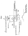
- FIG. 4 is a schematic diagram for explaining displacement detection and compensation using the position correction marker 270.
- the position correction marker 270 has the shape of a triangle with a side perpendicular to the main scanning direction.
- the line image sensor 230A and the line image sensor 230B have the overlapping area 240 in the main scanning direction.
- K is a reference position in the sub scanning direction
- the line image sensors 230A and 230B are displaced from the reference position K by Yl and Yr, respectively, in the sub scanning direction.
- the position correction marker 270 is read from the left side in the main scanning direction by the line image sensors 230A and 230B.
- the pixel before detection of the position correction marker 270 by the line image sensor 230A is X1
- the first pixel after detection of the position correction marker 270 by the line image sensor 230B is Xr
- the next pixel after the pixel Xl is defined as Xr, which enables combining data pieces of the two line image sensors 230A and 230B in the main scanning direction.
- the width of the position correction marker 270 in the reference position K in the sub scanning direction is Hk; the detected width of the position correction marker 270 by the line image sensor 230A is Hl; and the detected width of the position correction marker 270 by the line image sensor 230B is Hr. Since the position correction marker 270 has a triangular shape, the widths Hl and Hr are uniquely determined based on the position in the sub scanning direction. Accordingly, based on the values of the widths Hl and Hr detected by the line image sensors 230A and 230B, respectively, the number of lines corresponding to the displacement amount of each of the line image sensors 230A and 230B from the reference position K can be calculated.
- FIG. 5A is a schematic diagram illustrating the data arrangement in line buffers before displacement compensation
- FIG. 5B is a diagram illustrating the data arrangement in the line buffers after displacement compensation.
- liner image data obtained by each of the line image sensors 230A and 230B are stored in the corresponding line buffer ( FIG. 5A ).
- the starting addresses of outputs of the line buffers are increased or reduced to match the end edge images of the position correction marker 270. Compensation in the sub scanning direction can be performed in a similar manner.
- Displacement of less than one pixel can be compensated for by performing resampling in units of pixels or less. Resampling can be performed by two-dimensional interpolation using cubic function convolution, sinc function interpolation, linear interpolation or the like. This compensation can be performed in the main scanning direction and the sub scanning direction at the same time.
- the image quality may be improved by multiplying the image data of the overlapping area by a coefficient and performing image processing. Further, the image quality in the sub scanning direction may be improved by changing the number of pixels to be multiplied by a coefficient, changing the coefficient itself, and determining the necessity of image processing for each main scanning line.
- an image data correction device may perform displacement compensation when turning on the main power of an image forming apparatus or an image reading device. Creation of compensation data may be performed when the image forming apparatus or the image reading device is in the standby mode. This prevents displacement compensation from remaining unperformed for a long time.
- the reflection member 291 of the first stage includes the single continuous reflection mirror 311, which is arranged to cross the optical paths 280A and 280B.
- the reflection member 291 of the first stage may be formed of plural reflection mirrors.
- FIG. 6 is a schematic diagram illustrating a modified image reading device 400 according to an embodiment.
- FIG. 7 is a plan view illustrating a reflection member 411 of a first stage of the image reading device of FIG. 6 .
- the image reading device of this embodiment has the same configuration as the image reading device 200 of the embodiment described above except that the reflection member 411 includes two reflection mirrors 411A and 411B arranged in the main scanning direction and a connecting member 412 for connecting the reflection mirrors 411A and 411B.
- the two reflection mirrors 411A and 411B are disposed in the optical paths 280A and 280B, respectively, and the connecting member 412 is rotated by the motor 320 and the drive member 330. Therefore, it is possible to rotate the two reflection mirrors 411A and 411B at the same time to switch the position to be read by the line image sensors 230A and 230B between the document reading position A and the marker reading position B.
- the reflection mirrors 411A and 411B do not need to be so large and may be those commonly used for A3 size, which allows implementing this optical path changing configuration at low cost.
Landscapes
- Engineering & Computer Science (AREA)
- Multimedia (AREA)
- Signal Processing (AREA)
- Health & Medical Sciences (AREA)
- Biomedical Technology (AREA)
- General Health & Medical Sciences (AREA)
- Facsimile Scanning Arrangements (AREA)
- Image Input (AREA)
- Facsimile Heads (AREA)
Abstract
Description
- The present invention generally relates to an image reading device and an image forming apparatus, and particularly relates to an image reading device including an imaging element configured to focus a document image produced by reflection light of a document in a predetermined document reading position, plural line image sensors arranged in a main scanning direction in an imaging position of the document image to read the document image such that pieces of the document image read by the line image sensors overlap each other at adjacent ends in the main scanning direction, an optical system disposed between the document and the line image sensors to guide the reflection light to the line image sensors, and an image combining unit configured to combine plural image data pieces obtained by the plural line image sensors; and an image forming apparatus including the image reading device.
- Image reading devices read documents of various sizes. Some image reading devices read large documents such as A0 size documents.
- If the image reading devices are configured to read such a large document while moving an optical system, the image reading devices require not only a large size contact glass on which the document is placed but also a large size carriage for moving the optical system. Therefore, most of the image reading devices for large paper are configured to read a document using a contact line image sensor while moving the document.
- The contact line image sensor needs to have a length in the main scanning direction at least equal to the document width or greater. For example, to read an A0 size document, the length of the line image sensor needs to be 841 mm or greater. Producing such a line image sensor with one chip is technically difficult and results in increased costs.
- For this reason, a technique is used that acquires image information of an entire scanning line using plural small line image sensors arranged in the main scanning direction by focusing light beams from a scanning line of a document onto each of the line image sensors and electrically combining image signals read by the line image sensors. According to this technique using plural line image sensors, it is necessary that reading areas of adjacent line image sensors partially overlap each other in order to prevent a misalignment in a resulting image at a connection point between image data pieces read by the adjacent line image sensors.
-
FIGS. 8A and 8B are schematic diagrams illustrating the configuration of a related artimage reading device 100. Theimage reading device 100 includes twoimaging elements line image sensors reflection members contact glass 110 and theimaging element 150A. Similarly,reflection members optical path 180B between thecontact glass 110 and theimaging element 150B. - The
line image sensors reading width area 120 on the contact glass such that a portion of thereading width area 120 is read by both theline image sensors FIG. 8B ,reading width areas line image sensors overlapping area 140. Two image data pieces read and output from thereading width areas reading width area 120 by animage combining unit 160. - In the case of combining the image data pieces read by the plural
line image sensors overlapping area 140 of thereading width areas line image sensors 62-101170 56-126373 - As described above, it is possible to obtain an image without misalignment by arranging reading areas of adjacent line image sensors to partially overlap and electrically combining image signals read in the overlapping area. However, in the case where no image signal is read in the overlapping area of the reading areas of the line image sensors (in the case where there are no characters or images in the overlapping area), it is not possible to electrically combine the image signals.
- Furthermore, in the case of such an image reading device, even if the overlapping area of reading areas of line image sensors are precisely adjusted at the time of manufacturing, the reading areas of the line image sensors might be displaced due to vibration during transportation, deformation of the device body at the time of installation, or the like. The displacement of the reading areas varies the overlapping area, which causes misalignment in a resulting image. Moreover, imaging optical systems normally require conjugation length in the range of about 500 mm - 800 mm and have a reduction ratio of about 1/15. Accordingly, even a displacement of only 10 µm at the CCD side results in a displacement as great as 150 µm on the document surface.
- Displacement of the line image sensor is caused not only during manufacture, but also caused by thermal expansion due to temperature changes in the image reading device during use of the image reading device. Such displacement may occur in both the main scanning direction and the sub scanning direction.
- Japanese Laid-Open Patent Publication No.
2000-358140 - Japanese Laid-Open Patent Publication No.
2006-25289 - However, the image reading device of
Patent Document 3 needs to have an additional LED or lens for forming a marker as an image and the image reading device ofPatent Document 4 needs to have the marker irradiator for irradiating beams onto the correction patterns and therefore both the reading devices have an increased number of component parts. - Further, both the image reading devices of
Patent Documents - The present invention is directed toward providing an image reading device and an image forming apparatus capable of adjusting misalignment when combining images read by line image sensors and capable of preventing a marker from being incorporated as image information when reading a document.
- According to an aspect of the present invention, there is provided an image reading device that includes an imaging element configured to focus a document image produced by reflection light of a document in a predetermined document reading position; plural line image sensors arranged in a main scanning direction in an imaging position of the document image to read the document image such that pieces of the document image read by the line image sensors overlap each other at adjacent ends in the main scanning direction; an optical system disposed between the document and the line image sensors to guide the reflection light to the line image sensors; and an image combining unit configured to combine plural image data pieces obtained by the plural line image sensors. The image reading device is characterized in that a position correction marker is disposed in a marker reading position, which is a predetermined position different from the document reading position, in an area that can be read by the plural line image sensors; and the optical system includes an optical path changing unit configured to switch a reading position of the line image sensors between the document reading position and the marker reading position.
- According to another aspect of the present invention, there is provided an image forming apparatus that includes the above-described image reading device.
- The above-described image reading device and image forming apparatus can obtain data for image data connection without requiring a device for displaying a position correction marker or a device for moving the position correction marker.
-
-
FIG. 1 is a perspective view illustrating a wide digital copier as an image forming apparatus according to an embodiment of the present invention; -
FIGS. 2A and 2B are schematic diagrams illustrating an optical system of an image reading device according to an embodiment; -
FIG. 3 is a schematic side view illustrating an image reading device according to an embodiment; -
FIG. 4 is a schematic diagram for explaining displacement detection and compensation using a position correction marker; -
FIG. 5A is a schematic diagram illustrating the data arrangement in line buffers before displacement compensation; -
FIG. 5B is a schematic diagram illustrating the data arrangement in line buffers after displacement compensation; -
FIG. 6 is a schematic diagram illustrating a modified image reading device according to an embodiment; -
FIG. 7 is a plan view illustrating a reflection member of a first stage of the image reading device ofFIG. 6 ; and -
FIGS. 8A and 8B are schematic diagrams illustrating the configuration of a related art image reading device. - Preferred embodiments of the present invention are described below with reference to the accompanying drawings.
- An image forming apparatus according to an embodiment of the present invention is described with reference to the accompanying drawings.
FIG. 1 is a perspective view illustrating a wide digital copier as the image forming apparatus according to this embodiment of the present invention. As illustrated inFIG. 1 , the copier of this embodiment includes a document table 1 for document insertion and anoperations panel 2 at the front of the apparatus such that a user stands in front of the document table 1 and performs necessary operations such as pressing keys on theoperations panel 2 while inserting a document. The wide digital copier includes an image reading device for reading a document, a feeding device, an image forming device, a transfer device (not shown), and a fixing device in an apparatusmain body 4. - A user places a large sheet (e.g., A0 vertical size and A1 horizontal size) on the document table 1, and manually inserts the sheet into a
document unit 3 so that the sheet hits a predetermined point. Then, the document is transported to a reading position, in which the image surface of the document is read by the image reading device. After acquiring image data by this document scanning operation, the image forming apparatus causes the feeding device to feed a transfer sheet, causes the image forming device to execute an image formation process, causes the transfer device to transfer a toner image onto the transfer sheet, and causes the fixing unit to fix the toner image onto the transfer sheet, thereby performing an image forming operation. Note that the typical configurations and functions of the feeding device, the image forming device, the transfer device, and the fixing device in the apparatusmain body 4 are well known in the art and are not described herein. - Next, an image reading device is described.
FIGS. 2A and 2B are schematic diagrams illustrating an optical system of animage reading device 200 according to an embodiment.FIG. 3 is a schematic side view illustrating theimage reading device 200 of this embodiment. As shown inFIG. 2A , theimage reading device 200 includes twoline image sensors line image sensors reading width areas reading width area 220 of acontact glass 210, and image data pieces of these two imagereading width areas - Further, the
image reading device 200 includes an optical path changing unit (described below) in the optical system. As shown inFIG. 3 , theline image sensors position correction marker 270 for acquiring a position correction signal to be used when an image combining unit 260 (FIG. 2A ) combines images. - Further, the
image reading device 200 includes twoimaging lenses line image sensors platen 280 is disposed at the upper side of thecontact glass 210, and an illuminating device (not shown) for illuminating a document on thecontact glass 210 is disposed at the lower side of thecontact glass 210. - Between the
contact glass 210 and theimaging lenses reflection member 291 of a first stage,reflection members reflection members - As shown in
FIG. 2A , theimaging lenses reading width areas reading width area 220, onto theline image sensors FIG. 2B , the imagereading width areas area 240. The image of the overlappingarea 240 is read by both theline image sensors line image sensors image combining unit 260. Two image data pieces from theline image sensors image combining unit 260. - Plural reflection members are arranged in
optical paths contact glass 210 to theline image sensors reflection member 291 of the first stage, thereflection members reflection members contact glass 210 side. In this embodiment, thereflection members reflection members - The
position correction marker 270 is disposed, in the overlappingarea 240 in the main scanning direction, in a position spaced apart from the document reading position A by a predetermined distance on thecontact glass 210. The position in which theposition correction marker 270 is disposed is a marker reading position B. - The
position correction marker 270 has the shape of a triangle with a side perpendicular to the main scanning direction and is formed of a reduction unit for reducing the amount of only the light that passes through thecontact glass 210 by, for example, about 25% (seeFIG. 4 ). More specifically, theposition correction marker 270 is formed by firmly bonding, for example, a thin-film filter or an ND filter having a visible light transmission of about 75%, to thecontact glass 210 through uniform application of transparent adhesive. - Next, the optical path changing unit is described. The optical path changing unit is implemented as the
first reflection member 291, amotor 320, and adrive member 330 that is driven by themotor 320 to rotate asubstrate 312. - The reason for the reflection member closest to the reading position, namely, the
reflection member 291 of the first stage, being used as the optical path changing unit is as follows. In the case of changing an optical path by rotating a reflection member, if there is an error in the rotational angle, the position from which information is read is displaced from a predetermined reading position. Such displacement due to an error in the rotational angle is proportional to the optical path length. Accordingly, the smaller the distance between a reflection member to be rotated and the document reading position A is, the smaller the displacement can be. Therefore, in this embodiment, thereflection member 291 of the first stage closest to the reading position is used as the optical path changing unit, thereby reducing the effects of rotational angle errors and improving the image reading accuracy. - As shown in
FIG. 3 , thereflection member 291 includes thesubstrate 312 rotatably supported by asupport point 313, and a seamlesscontinuous reflection mirror 311 for reflecting all the light reflected from the imagereading width area 220. Themotor 320 is driven by a control device (not shown) to advance and retract the drive member 330 (the arrows C). Advancement and retraction of thedrive member 330 cause thereflection member 291 to swing (the arrows D), thereby switching (the arrows F) the light to be incident on theline image sensors FIG. 3 ) from the predetermined document reading position A and marker reading position B on thecontact glass 210. Note that the orientation of thereflection member reflection members continuous reflection mirror 311 is used in thereflection member 291, it is possible to change the angles of theoptical paths line image sensors line image sensors - Further, in this embodiment, the optical path length from the
imaging lenses imaging lenses position correction marker 270 can be read under the same conditions and hence at the same focus depth. Therefore, it is possible to improve the image adjustment accuracy. - Operations of the
image reading device 200 of this embodiment are described below. First, an operation of reading theposition correction marker 270 is described. To read theposition correction marker 270, themotor 320 is driven by the control device (not shown) to cause thedrive member 330 to rotate thereflection member 291 such that the reflection light from the marker reading position B is made incident on theline image sensors FIG. 3 ). Then, the image of theposition correction marker 270 in the marker reading position B is focused onto theline image sensors imaging lenses position correction marker 270. Thus, data for correcting two image data pieces to be obtained by theline image sensors - Next, an operation of reading a document is described. To read a document, the
motor 320 is driven by the control device (not shown) to cause thedrive member 330 to rotate thereflection member 291 such that the reflection light from the document reading position A is made incident on theline image sensors FIG. 3 ). Then, while transporting the document between thecontact glass 210 and theplaten 280, a document image in the document reading position A is focused onto theline image sensors imaging lenses reflection members 291 of the first stage, thereflection members reflection members line image sensors imaging lenses - The
line image sensors reading width areas area 240. Adjustment for preventing displacement in the sub scanning direction is performed at the time of manufacturing. The adjustment in the sub scanning direction is performed by adjusting the positions and angles of theimaging lenses line image sensors - Displacement compensation in the main scanning direction is described below. The conjugation length of an imaging optical system is as great as about 600 mm and therefore, if the
line image sensors imaging lenses contact glass 210 is easily displaced by 1 dot or greater, which results in image degradation. In particular, vibration during transportation of the device and thermal expansion due to temperature change in the device tend to cause displacement. - In this embodiment, such displacement of the optical system is detected and compensated for.
FIG. 4 is a schematic diagram for explaining displacement detection and compensation using theposition correction marker 270. In this embodiment, as mentioned above, theposition correction marker 270 has the shape of a triangle with a side perpendicular to the main scanning direction. - The
line image sensor 230A and theline image sensor 230B have the overlappingarea 240 in the main scanning direction. When K is a reference position in the sub scanning direction, theline image sensors - With regard to compensation in the main scanning direction, suppose that the
position correction marker 270 is read from the left side in the main scanning direction by theline image sensors position correction marker 270 by theline image sensor 230A is X1 and the first pixel after detection of theposition correction marker 270 by theline image sensor 230B is Xr, the next pixel after the pixel Xl is defined as Xr, which enables combining data pieces of the twoline image sensors - With regard to compensation in the sub scanning direction, the width of the
position correction marker 270 in the reference position K in the sub scanning direction is Hk; the detected width of theposition correction marker 270 by theline image sensor 230A is Hl; and the detected width of theposition correction marker 270 by theline image sensor 230B is Hr. Since theposition correction marker 270 has a triangular shape, the widths Hl and Hr are uniquely determined based on the position in the sub scanning direction. Accordingly, based on the values of the widths Hl and Hr detected by theline image sensors line image sensors - Next, an operation of compensating for displacement in units of pixels in the main scanning direction using the
position correction marker 270 is described.FIG. 5A is a schematic diagram illustrating the data arrangement in line buffers before displacement compensation, andFIG. 5B is a diagram illustrating the data arrangement in the line buffers after displacement compensation. In this operation, liner image data obtained by each of theline image sensors FIG. 5A ). There is a displacement of 4 pixels between end edge images (shaded regions inFIG. 5A ) of theposition correction marker 270, which is a reference for displacement of theline image sensors line image sensors position correction marker 270. Compensation in the sub scanning direction can be performed in a similar manner. - In the
image reading device 200 of this embodiment, it is possible to compensate for displacement of less than one pixel. Displacement of less than one pixel can be compensated for by performing resampling in units of pixels or less. Resampling can be performed by two-dimensional interpolation using cubic function convolution, sinc function interpolation, linear interpolation or the like. This compensation can be performed in the main scanning direction and the sub scanning direction at the same time. - After compensation for displacement of two optical systems in the main scanning direction, a density boundary might appear at the connection point in the main scanning direction. The image quality may be improved by multiplying the image data of the overlapping area by a coefficient and performing image processing. Further, the image quality in the sub scanning direction may be improved by changing the number of pixels to be multiplied by a coefficient, changing the coefficient itself, and determining the necessity of image processing for each main scanning line.
- According to an embodiment of the present invention, an image data correction device may perform displacement compensation when turning on the main power of an image forming apparatus or an image reading device. Creation of compensation data may be performed when the image forming apparatus or the image reading device is in the standby mode. This prevents displacement compensation from remaining unperformed for a long time.
- In the
image reading device 200, thereflection member 291 of the first stage includes the singlecontinuous reflection mirror 311, which is arranged to cross theoptical paths reflection member 291 of the first stage may be formed of plural reflection mirrors.FIG. 6 is a schematic diagram illustrating a modifiedimage reading device 400 according to an embodiment.FIG. 7 is a plan view illustrating a reflection member 411 of a first stage of the image reading device ofFIG. 6 . The image reading device of this embodiment has the same configuration as theimage reading device 200 of the embodiment described above except that the reflection member 411 includes two reflection mirrors 411A and 411B arranged in the main scanning direction and a connectingmember 412 for connecting the reflection mirrors 411A and 411B. In this embodiment, the two reflection mirrors 411A and 411B are disposed in theoptical paths member 412 is rotated by themotor 320 and thedrive member 330. Therefore, it is possible to rotate the two reflection mirrors 411A and 411B at the same time to switch the position to be read by theline image sensors - In this embodiment, the reflection mirrors 411A and 411B do not need to be so large and may be those commonly used for A3 size, which allows implementing this optical path changing configuration at low cost.
Claims (9)
- An image reading device comprising:an imaging element configured to focus a document image produced by reflection light of a document in a predetermined document reading position; plural line image sensors arranged in a main scanning direction in an imaging position of the document image to read the document image such that pieces of the document image read by the line image sensors overlap each other at adjacent ends in the main scanning direction; an optical system disposed between the document and the line image sensors to guide the reflection light to the line image sensors; and an image combining unit configured to combine plural image data pieces obtained by the plural line image sensors, the image reading device beingcharacterized in that:a position correction marker is disposed in a marker reading position, which is a predetermined position different from the document reading position, in an area that can be read by the plural line image sensors; andthe optical system includes an optical path changing unit configured to switch a reading position of the line image sensors between the document reading position and the marker reading position.
- An image reading device as claimed in claim 1, characterized in that:the optical system includes a reflection member configured to fold an optical path; andthe optical path changing unit includes the reflection member and a driving and rotating unit configured to drive and rotate the reflection member.
- An image reading device as claimed in claim 2, characterized in that the reflection member of the optical path changing unit includes a continuous reflection mirror configured to direct all the reflection light from the document reading position to the line image sensors.
- An image reading device as claimed in claim 2, characterized in that the reflection member of the optical path changing unit includes plural reflection mirrors arranged in the main scanning direction, and a connecting member connecting the reflection mirrors such that the reflection mirrors are driven and rotated together by the driving and rotating unit.
- An image reading device as claimed in any one of claims 1 to 4, characterized in that:the optical system includes plural reflection members; andthe reflection member included in the optical path changing unit is one of the plural reflection members that is closest to the document reading position.
- An image reading device as claimed in any one of claims 1 to 5, characterized in that a length of an optical path from the imaging element to the marker reading position is equal to a length of an optical path from the imaging element to the document reading position.
- An image reading device as claimed in any one of claims 1 to 6, characterized in that the image combining unit includes a connection position determining unit configured to determine a connection position of each of the image data pieces of the line image sensors in units of pixels of the line image sensors based on positional information detected using the position correction marker.
- An image reading device as claimed in any one of claims 1 to 6, characterized in that the image combining unit includes a connection position determining unit configured to determine a connection position of each of the image data pieces of the line image sensors in units of pixels of the line image sensors based on positional information detected using the position correction marker, and a compensating unit configured to compensate for a relative displacement of less than one pixel using image interpolation.
- An image forming apparatus characterized in that it comprises an image reading device according to any one of claims 1 to 8.
Applications Claiming Priority (1)
| Application Number | Priority Date | Filing Date | Title |
|---|---|---|---|
| JP2008030339A JP4864021B2 (en) | 2008-02-12 | 2008-02-12 | Image reading apparatus and image forming apparatus |
Publications (2)
| Publication Number | Publication Date |
|---|---|
| EP2091223A1 true EP2091223A1 (en) | 2009-08-19 |
| EP2091223B1 EP2091223B1 (en) | 2013-09-11 |
Family
ID=40548827
Family Applications (1)
| Application Number | Title | Priority Date | Filing Date |
|---|---|---|---|
| EP20090250316 Ceased EP2091223B1 (en) | 2008-02-12 | 2009-02-09 | Image reading device and image forming apparatus |
Country Status (3)
| Country | Link |
|---|---|
| EP (1) | EP2091223B1 (en) |
| JP (1) | JP4864021B2 (en) |
| CN (1) | CN101510936B (en) |
Cited By (15)
| Publication number | Priority date | Publication date | Assignee | Title |
|---|---|---|---|---|
| EP2423756A1 (en) * | 2010-08-23 | 2012-02-29 | Ricoh Company, Limited | Image reading device and image forming incorporating same |
| WO2012041390A1 (en) | 2010-10-01 | 2012-04-05 | Contex A/S | Signal intensity matching of image sensors |
| US20180063358A1 (en) * | 2016-08-29 | 2018-03-01 | Seiko Epson Corporation | Scanner, and image data generating method |
| EP3291526A1 (en) * | 2016-08-29 | 2018-03-07 | Seiko Epson Corporation | Scanner, and image data generating method |
| US9998626B2 (en) | 2016-02-02 | 2018-06-12 | Seiko Epson Corporation | Scanner and method of generating image data |
| US10097721B2 (en) | 2016-09-01 | 2018-10-09 | Seiko Epson Corporation | Scanner, and image data generating method |
| US10298802B2 (en) | 2016-06-28 | 2019-05-21 | Seiko Epson Corporation | Scanner including multiple sensors |
| US10397434B2 (en) | 2017-01-23 | 2019-08-27 | Seiko Epson Corporation | Scanner that combines images read by first and second sensor arrays, scan program, and method of producing scan data |
| US10447885B2 (en) | 2016-08-29 | 2019-10-15 | Seiko Epson Corporation | Scanner system and image data generating method |
| US10477057B2 (en) | 2017-05-30 | 2019-11-12 | Seiko Corporation | Scanner and scanner data generating method |
| US10506127B2 (en) | 2017-05-30 | 2019-12-10 | Seiko Epson Corporation | Scanner including first sensor to read first document when placed on platen glass and second and third sensors to read second document when moving along conveyance path, and scanner data generating method |
| US10587771B2 (en) | 2017-05-30 | 2020-03-10 | Seiko Epson Corporartion | Scanner and scanner data generating method |
| US10594893B2 (en) | 2017-01-23 | 2020-03-17 | Seiko Epson Corporation | Scanner, scan program, and method of producing scan data |
| US10659653B2 (en) | 2017-01-23 | 2020-05-19 | Seiko Epson Corporation | Scanner that combines images read by first and second sensor arrays, scan program, and method of producing scan data |
| CN111526258A (en) * | 2019-02-04 | 2020-08-11 | 京瓷办公信息系统株式会社 | image forming apparatus |
Families Citing this family (7)
| Publication number | Priority date | Publication date | Assignee | Title |
|---|---|---|---|---|
| JP5495710B2 (en) * | 2009-10-22 | 2014-05-21 | 三菱電機株式会社 | Image combination apparatus and image combination position calculation method |
| WO2011147049A1 (en) | 2010-05-27 | 2011-12-01 | Colortrac Limited | Document scanner |
| WO2011147050A1 (en) * | 2010-05-27 | 2011-12-01 | Colortrac Limited | Document scanner |
| EP3213498A4 (en) * | 2014-10-30 | 2018-05-30 | Hewlett-Packard Development Company, L.P. | Determining coordinates of scan bars |
| WO2017106761A1 (en) * | 2015-12-18 | 2017-06-22 | Digital Domain, Inc. | Systems and methods for multi-sensor image capture |
| JP6828290B2 (en) * | 2016-07-06 | 2021-02-10 | コニカミノルタ株式会社 | Image reader, distance adjustment method and distance adjustment program between the document and the light receiving sensor in the device |
| CN110133843A (en) * | 2019-04-30 | 2019-08-16 | 联想图像(天津)科技有限公司 | A kind of laser scan unit and laser printer |
Citations (9)
| Publication number | Priority date | Publication date | Assignee | Title |
|---|---|---|---|---|
| JPS5613870A (en) * | 1979-07-16 | 1981-02-10 | Ricoh Co Ltd | Solid state scanner |
| JPS56126373A (en) | 1980-03-10 | 1981-10-03 | Canon Inc | Picture reading device |
| JPS5799080A (en) * | 1980-12-12 | 1982-06-19 | Nec Corp | Automatic compensation system for joint position in facsimile transmitter |
| US4465939A (en) * | 1980-08-25 | 1984-08-14 | Canon Kabushiki Kaisha | Image reading apparatus having a plurality of image sensors |
| JPS62101170A (en) | 1985-10-28 | 1987-05-11 | Toshiba Corp | Picture reader |
| US4675745A (en) * | 1983-09-19 | 1987-06-23 | Canon Kabushiki Kaisha | Image reading apparatus |
| US5942746A (en) * | 1997-08-11 | 1999-08-24 | Mustek Systems, Inc. | Multi-lenses optical device |
| JP2000358140A (en) | 1999-04-13 | 2000-12-26 | Matsushita Electric Ind Co Ltd | Image reading position adjusting method, image reading method, and image reading apparatus |
| JP2006025289A (en) | 2004-07-09 | 2006-01-26 | Matsushita Electric Ind Co Ltd | Marker device and image reading device having the same |
Family Cites Families (3)
| Publication number | Priority date | Publication date | Assignee | Title |
|---|---|---|---|---|
| JPS54101225A (en) * | 1978-01-26 | 1979-08-09 | Ricoh Co Ltd | Original read-in method |
| JPS63217871A (en) * | 1987-03-06 | 1988-09-09 | Fujitsu Ltd | Original carrier type picture reader |
| NL1004831C2 (en) * | 1996-12-19 | 1998-06-22 | Oce Tech Bv | Scanner system with automatic position error compensation. |
-
2008
- 2008-02-12 JP JP2008030339A patent/JP4864021B2/en not_active Expired - Fee Related
-
2009
- 2009-02-06 CN CN2009100057757A patent/CN101510936B/en not_active Expired - Fee Related
- 2009-02-09 EP EP20090250316 patent/EP2091223B1/en not_active Ceased
Patent Citations (9)
| Publication number | Priority date | Publication date | Assignee | Title |
|---|---|---|---|---|
| JPS5613870A (en) * | 1979-07-16 | 1981-02-10 | Ricoh Co Ltd | Solid state scanner |
| JPS56126373A (en) | 1980-03-10 | 1981-10-03 | Canon Inc | Picture reading device |
| US4465939A (en) * | 1980-08-25 | 1984-08-14 | Canon Kabushiki Kaisha | Image reading apparatus having a plurality of image sensors |
| JPS5799080A (en) * | 1980-12-12 | 1982-06-19 | Nec Corp | Automatic compensation system for joint position in facsimile transmitter |
| US4675745A (en) * | 1983-09-19 | 1987-06-23 | Canon Kabushiki Kaisha | Image reading apparatus |
| JPS62101170A (en) | 1985-10-28 | 1987-05-11 | Toshiba Corp | Picture reader |
| US5942746A (en) * | 1997-08-11 | 1999-08-24 | Mustek Systems, Inc. | Multi-lenses optical device |
| JP2000358140A (en) | 1999-04-13 | 2000-12-26 | Matsushita Electric Ind Co Ltd | Image reading position adjusting method, image reading method, and image reading apparatus |
| JP2006025289A (en) | 2004-07-09 | 2006-01-26 | Matsushita Electric Ind Co Ltd | Marker device and image reading device having the same |
Cited By (20)
| Publication number | Priority date | Publication date | Assignee | Title |
|---|---|---|---|---|
| US8576419B2 (en) | 2010-08-23 | 2013-11-05 | Ricoh Company, Limited | Image reading device and image forming apparatus for detecting that document reading unit is positioned at document reference line |
| EP2423756A1 (en) * | 2010-08-23 | 2012-02-29 | Ricoh Company, Limited | Image reading device and image forming incorporating same |
| WO2012041390A1 (en) | 2010-10-01 | 2012-04-05 | Contex A/S | Signal intensity matching of image sensors |
| US9998626B2 (en) | 2016-02-02 | 2018-06-12 | Seiko Epson Corporation | Scanner and method of generating image data |
| US10298802B2 (en) | 2016-06-28 | 2019-05-21 | Seiko Epson Corporation | Scanner including multiple sensors |
| US10506125B2 (en) | 2016-06-28 | 2019-12-10 | Seiko Epson Corporation | Sensor chip including multiple photoelectric conversion elements |
| EP3291526A1 (en) * | 2016-08-29 | 2018-03-07 | Seiko Epson Corporation | Scanner, and image data generating method |
| EP3291525A1 (en) * | 2016-08-29 | 2018-03-07 | Seiko Epson Corporation | Scanner, and image data generating method |
| US10158766B2 (en) | 2016-08-29 | 2018-12-18 | Seiko Epson Corporation | Scanner, and image data generating method |
| US20180063358A1 (en) * | 2016-08-29 | 2018-03-01 | Seiko Epson Corporation | Scanner, and image data generating method |
| US10447885B2 (en) | 2016-08-29 | 2019-10-15 | Seiko Epson Corporation | Scanner system and image data generating method |
| US10455107B2 (en) * | 2016-08-29 | 2019-10-22 | Seiko Epson Corporation | Scanner having a merging mark and white reference to correct output of the sensor chip |
| US10097721B2 (en) | 2016-09-01 | 2018-10-09 | Seiko Epson Corporation | Scanner, and image data generating method |
| US10397434B2 (en) | 2017-01-23 | 2019-08-27 | Seiko Epson Corporation | Scanner that combines images read by first and second sensor arrays, scan program, and method of producing scan data |
| US10594893B2 (en) | 2017-01-23 | 2020-03-17 | Seiko Epson Corporation | Scanner, scan program, and method of producing scan data |
| US10659653B2 (en) | 2017-01-23 | 2020-05-19 | Seiko Epson Corporation | Scanner that combines images read by first and second sensor arrays, scan program, and method of producing scan data |
| US10477057B2 (en) | 2017-05-30 | 2019-11-12 | Seiko Corporation | Scanner and scanner data generating method |
| US10506127B2 (en) | 2017-05-30 | 2019-12-10 | Seiko Epson Corporation | Scanner including first sensor to read first document when placed on platen glass and second and third sensors to read second document when moving along conveyance path, and scanner data generating method |
| US10587771B2 (en) | 2017-05-30 | 2020-03-10 | Seiko Epson Corporartion | Scanner and scanner data generating method |
| CN111526258A (en) * | 2019-02-04 | 2020-08-11 | 京瓷办公信息系统株式会社 | image forming apparatus |
Also Published As
| Publication number | Publication date |
|---|---|
| JP4864021B2 (en) | 2012-01-25 |
| CN101510936B (en) | 2011-09-07 |
| JP2009194434A (en) | 2009-08-27 |
| EP2091223B1 (en) | 2013-09-11 |
| CN101510936A (en) | 2009-08-19 |
Similar Documents
| Publication | Publication Date | Title |
|---|---|---|
| EP2091223B1 (en) | Image reading device and image forming apparatus | |
| EP2086213B1 (en) | Image reading apparatus, and image forming apparatus | |
| US20110080476A1 (en) | High Performance Vision System for Part Registration | |
| EP0963101A2 (en) | Image sensor module adjustable to six degrees of freedom for use with an image acquisition device | |
| US7505184B2 (en) | Adjusting method of image reading apparatus and image reading apparatus | |
| US20090180156A1 (en) | Image reading apparatus and image forming apparatus | |
| JP7183669B2 (en) | Image reading device, image forming device and image reading method | |
| US12169370B2 (en) | Exposure control in photolithographic direct exposure methods for manufacturing circuit boards or circuits | |
| EP1381214B1 (en) | Reflective imaging optical system with folded beam path and image reading apparatus using the same | |
| US6600568B1 (en) | System and method of measuring image sensor chip shift | |
| JP5322885B2 (en) | Image combination apparatus and image combination position calculation method | |
| JP3719020B2 (en) | Image data correction method in image reading apparatus | |
| JP2009171171A (en) | Image reading apparatus and image forming apparatus | |
| US6317219B1 (en) | Method and apparatus for compensating for a distortion between blocks of a scanned image | |
| JP4161595B2 (en) | Image reading device | |
| JP5495710B2 (en) | Image combination apparatus and image combination position calculation method | |
| JP2009188829A (en) | Image reading apparatus and image forming apparatus | |
| US6384942B1 (en) | Image scanning unit | |
| JP3200020B2 (en) | Laser writing system with orthogonality correction function in main scanning direction and sub scanning direction | |
| JPH07183992A (en) | Image reader | |
| US6728011B1 (en) | Method of adjusting scanner module and device thereof | |
| JPS6313571A (en) | Chart for adjusting optical system of image reader | |
| JP2006025289A (en) | Marker device and image reading device having the same | |
| JPH0923318A (en) | Image reading device | |
| JP2002344702A (en) | Image reading device |
Legal Events
| Date | Code | Title | Description |
|---|---|---|---|
| PUAI | Public reference made under article 153(3) epc to a published international application that has entered the european phase |
Free format text: ORIGINAL CODE: 0009012 |
|
| 17P | Request for examination filed |
Effective date: 20090216 |
|
| AK | Designated contracting states |
Kind code of ref document: A1 Designated state(s): AT BE BG CH CY CZ DE DK EE ES FI FR GB GR HR HU IE IS IT LI LT LU LV MC MK MT NL NO PL PT RO SE SI SK TR |
|
| AX | Request for extension of the european patent |
Extension state: AL BA RS |
|
| 17Q | First examination report despatched |
Effective date: 20090923 |
|
| AKX | Designation fees paid |
Designated state(s): DK ES FR GB IT NL |
|
| REG | Reference to a national code |
Ref country code: DE Ref legal event code: 8566 |
|
| REG | Reference to a national code |
Ref country code: DE Ref legal event code: R079 Free format text: PREVIOUS MAIN CLASS: H04N0001193000 Ipc: H04N0001000000 |
|
| GRAP | Despatch of communication of intention to grant a patent |
Free format text: ORIGINAL CODE: EPIDOSNIGR1 |
|
| RIC1 | Information provided on ipc code assigned before grant |
Ipc: H04N 1/00 20060101AFI20130311BHEP Ipc: H04N 1/191 20060101ALI20130311BHEP |
|
| INTG | Intention to grant announced |
Effective date: 20130416 |
|
| GRAS | Grant fee paid |
Free format text: ORIGINAL CODE: EPIDOSNIGR3 |
|
| GRAA | (expected) grant |
Free format text: ORIGINAL CODE: 0009210 |
|
| AK | Designated contracting states |
Kind code of ref document: B1 Designated state(s): DK ES FR GB IT NL |
|
| REG | Reference to a national code |
Ref country code: GB Ref legal event code: FG4D |
|
| REG | Reference to a national code |
Ref country code: NL Ref legal event code: VDEP Effective date: 20130911 |
|
| PG25 | Lapsed in a contracting state [announced via postgrant information from national office to epo] |
Ref country code: NL Free format text: LAPSE BECAUSE OF FAILURE TO SUBMIT A TRANSLATION OF THE DESCRIPTION OR TO PAY THE FEE WITHIN THE PRESCRIBED TIME-LIMIT Effective date: 20130911 |
|
| PG25 | Lapsed in a contracting state [announced via postgrant information from national office to epo] |
Ref country code: ES Free format text: LAPSE BECAUSE OF FAILURE TO SUBMIT A TRANSLATION OF THE DESCRIPTION OR TO PAY THE FEE WITHIN THE PRESCRIBED TIME-LIMIT Effective date: 20130911 |
|
| PLBE | No opposition filed within time limit |
Free format text: ORIGINAL CODE: 0009261 |
|
| STAA | Information on the status of an ep patent application or granted ep patent |
Free format text: STATUS: NO OPPOSITION FILED WITHIN TIME LIMIT |
|
| 26N | No opposition filed |
Effective date: 20140612 |
|
| PG25 | Lapsed in a contracting state [announced via postgrant information from national office to epo] |
Ref country code: IT Free format text: LAPSE BECAUSE OF FAILURE TO SUBMIT A TRANSLATION OF THE DESCRIPTION OR TO PAY THE FEE WITHIN THE PRESCRIBED TIME-LIMIT Effective date: 20130911 |
|
| PG25 | Lapsed in a contracting state [announced via postgrant information from national office to epo] |
Ref country code: DK Free format text: LAPSE BECAUSE OF FAILURE TO SUBMIT A TRANSLATION OF THE DESCRIPTION OR TO PAY THE FEE WITHIN THE PRESCRIBED TIME-LIMIT Effective date: 20130911 |
|
| REG | Reference to a national code |
Ref country code: FR Ref legal event code: PLFP Year of fee payment: 8 |
|
| REG | Reference to a national code |
Ref country code: FR Ref legal event code: PLFP Year of fee payment: 9 |
|
| REG | Reference to a national code |
Ref country code: FR Ref legal event code: PLFP Year of fee payment: 10 |
|
| PGFP | Annual fee paid to national office [announced via postgrant information from national office to epo] |
Ref country code: GB Payment date: 20180216 Year of fee payment: 10 |
|
| PGFP | Annual fee paid to national office [announced via postgrant information from national office to epo] |
Ref country code: FR Payment date: 20180223 Year of fee payment: 10 |
|
| GBPC | Gb: european patent ceased through non-payment of renewal fee |
Effective date: 20190209 |
|
| PG25 | Lapsed in a contracting state [announced via postgrant information from national office to epo] |
Ref country code: GB Free format text: LAPSE BECAUSE OF NON-PAYMENT OF DUE FEES Effective date: 20190209 |
|
| PG25 | Lapsed in a contracting state [announced via postgrant information from national office to epo] |
Ref country code: FR Free format text: LAPSE BECAUSE OF NON-PAYMENT OF DUE FEES Effective date: 20190228 |