EP2089770B1 - Method of creating photolithographic structures with developer-trimmed hard mask - Google Patents
Method of creating photolithographic structures with developer-trimmed hard mask Download PDFInfo
- Publication number
- EP2089770B1 EP2089770B1 EP07843009.7A EP07843009A EP2089770B1 EP 2089770 B1 EP2089770 B1 EP 2089770B1 EP 07843009 A EP07843009 A EP 07843009A EP 2089770 B1 EP2089770 B1 EP 2089770B1
- Authority
- EP
- European Patent Office
- Prior art keywords
- hard mask
- layer
- substrate
- substrate surface
- light
- Prior art date
- Legal status (The legal status is an assumption and is not a legal conclusion. Google has not performed a legal analysis and makes no representation as to the accuracy of the status listed.)
- Active
Links
Images


Classifications
-
- G—PHYSICS
- G03—PHOTOGRAPHY; CINEMATOGRAPHY; ANALOGOUS TECHNIQUES USING WAVES OTHER THAN OPTICAL WAVES; ELECTROGRAPHY; HOLOGRAPHY
- G03F—PHOTOMECHANICAL PRODUCTION OF TEXTURED OR PATTERNED SURFACES, e.g. FOR PRINTING, FOR PROCESSING OF SEMICONDUCTOR DEVICES; MATERIALS THEREFOR; ORIGINALS THEREFOR; APPARATUS SPECIALLY ADAPTED THEREFOR
- G03F7/00—Photomechanical, e.g. photolithographic, production of textured or patterned surfaces, e.g. printing surfaces; Materials therefor, e.g. comprising photoresists; Apparatus specially adapted therefor
- G03F7/004—Photosensitive materials
- G03F7/09—Photosensitive materials characterised by structural details, e.g. supports, auxiliary layers
- G03F7/11—Photosensitive materials characterised by structural details, e.g. supports, auxiliary layers having cover layers or intermediate layers, e.g. subbing layers
-
- H—ELECTRICITY
- H10—SEMICONDUCTOR DEVICES; ELECTRIC SOLID-STATE DEVICES NOT OTHERWISE PROVIDED FOR
- H10P—GENERIC PROCESSES OR APPARATUS FOR THE MANUFACTURE OR TREATMENT OF DEVICES COVERED BY CLASS H10
- H10P14/00—Formation of materials, e.g. in the shape of layers or pillars
- H10P14/60—Formation of materials, e.g. in the shape of layers or pillars of insulating materials
- H10P14/68—Organic materials, e.g. photoresists
- H10P14/683—Organic materials, e.g. photoresists carbon-based polymeric organic materials, e.g. polyimides, poly cyclobutene or PVC
-
- H—ELECTRICITY
- H10—SEMICONDUCTOR DEVICES; ELECTRIC SOLID-STATE DEVICES NOT OTHERWISE PROVIDED FOR
- H10P—GENERIC PROCESSES OR APPARATUS FOR THE MANUFACTURE OR TREATMENT OF DEVICES COVERED BY CLASS H10
- H10P76/00—Manufacture or treatment of masks on semiconductor bodies, e.g. by lithography or photolithography
-
- H—ELECTRICITY
- H10—SEMICONDUCTOR DEVICES; ELECTRIC SOLID-STATE DEVICES NOT OTHERWISE PROVIDED FOR
- H10P—GENERIC PROCESSES OR APPARATUS FOR THE MANUFACTURE OR TREATMENT OF DEVICES COVERED BY CLASS H10
- H10P76/00—Manufacture or treatment of masks on semiconductor bodies, e.g. by lithography or photolithography
- H10P76/20—Manufacture or treatment of masks on semiconductor bodies, e.g. by lithography or photolithography of masks comprising organic materials
Definitions
- the present invention is broadly concerned with methods that utilize hard mask compositions to form structures on semiconductor substrates.
- DOF is a very practical matter that determines the robustness of photolithographic processes and ultimately the yield of final devices.
- the photoresist thickness must be reduced.
- a limit exists for photoresist thickness reduction in the traditional single-layer scheme The limit is determined by etch depth and selectivity ofphotoresist to substrate. Etch selectivities of ArF photoresists have been improved significantly in the last few years while further improvement of organic polymer-based photoresists has been marginal.
- WO 2005/001901 A2 discloses a method of forming a precursor structure for use in microelectronic applications. Said method comprises the steps of providing a substrate having a surface, applying a protective layer to said substrate surface, and applying a photoresist to said protective layer, said photoresist having a thickness of less than 150 nm.
- the protective layer material is made of a polymeric, photosensitive material comprising a light attenuating moiety in the polymer molecule.
- US 2003/235786 A1 discloses a method of forming an integrated circuit precursor structure. Said method comprises among other steps forming a coating on a substrate, forming a photoresist layer on said coating.
- the coating is formed from a composition comprising a solvent system and a polymer dissolved or dispersed in said solvent system.
- Said polymer includes a photosensitive polymeric material containing a light attenuating moiety in its polymer molecule.
- WO 2004/001806 A2 also discloses such a method of using a composition in photolithographic processes.
- the polymeric material used in said composition contains a photosensitive polymeric material containing a light attenuating moiety in its polymer molecule.
- V.V. Aristov et al. Multilayer Resists with Variable Layer Parameters for Submicron Lithography
- Microelectronic Engineering, vol. 11, April 30, 1990, pages 553 to 556 describe the properties of methyl acrylate-methacrylic acid copolymer used as resist in submicron lithography.
- EP 0 092 782 A2 discloses a composition useful as hardmask layer.
- Said layer may comprise among other components titanium acetyl acetonate, ethyl cellosolve, trimethylolpropane triacrylate, stearic acid and a solvent system.
- the hardmask is used to transfer an image through printing to an external surface.
- DuPont Tyzor Orgsnic Titanates General Brochure 2001, pages 1 to 11 , discloses titanium compounds used in applications such as catalysis, polymer crosslinking agents, surface modification, coatings, adhesives, printing inks and reagents.
- the present invention overcomes the problems of the prior art by providing a method of forming a microelectronic structure, said method comprising: applying a first composition to a microelectronic substrate (10) or to an intermediate layer on said microelectronic substrate (10) to form a hard mask layer (18) thereon, applying an imaging layer (22) to said hard mask layer (18), or to intermediate layers on said hard mask (18); and selectively exposing said imaging layer (22) to light having a wavelength of from 400 nm to 10 nm to yield light-exposed portions of the imaging layer (22); the method being characterized in that said first composition comprises: (A) where:
- the present invention is concerned with the use of compositions that are useful as hard masks during the fabrication of microelectronic devices.
- composition used comprises where M is selected from the group consisting of Ti and Zr, and each R is individually selected from the group consisting of hydrogen and branched or unbranched C 1 to C 12 alkyls, preferably from about C 1 to about C 6 .
- R is selected from the group consisting of hydrogen, -CH 3 , and -C 3 H 7 , (available from DuPont under the name TyzorTM).
- the composition preferably comprises from about 1 % to about 20% by weight of Formula (I), more preferably from about 2% to about 15% by weight of Formula (I), and even more preferably from about 3% to about 10% by weight, based upon the total weight of the composition taken as 100% by weight. More particularly, Formula (I) is included at levels to yield levels of M of from about 5% to about 40% by weight, and more preferably from about 10% to about 30% by weight, based upon the total weight of the solids taken as 100% by weight.
- the composition also comprises a compound (II) that includes at least one -OH group and an alkoxy group that can form covalent bonds with M of Formula (I) above.
- groups include -OR 1 , where R 1 is selected from the group consisting of hydrogen and (branched or unbranched C 1 to C 12 alkyls, preferably from about C 1 to about C 6 . In a particularly preferred embodiment, these groups are -OH and -OC 2 H 5 .
- This compound (II) should be of electronic grade and should also be stable in the hard mask formulation. That is, the compound should remain in solution at ambient storage conditions (i.e., 20-25°C) for at least about 30 days.
- This compound (II) is important for development rate control. That is, using higher quantities of the compound will yield a composition with a faster development rate, while using lower quantities of the compound will yield a composition with a slower development rate.
- One of ordinary skill in the art can adjust the quantity of the compound to obtain the desired development rate for the particular process being carried out.
- the quantity of the compound will generally be from about 0.1 % to about 15% by weight, more preferably from about 0.2% to about 10% by weight, and even more preferably from about 0.2% to about 2% by weight, based upon the total weight of the composition taken as 100% by weight.
- this compound (II) can also include light attenuating moieties selected to absorb light of a desired wavelength. These moieties can be selected to absorb light at wavelengths of from about 400 nm to about 10 nm, and examples of suitable light absorbing moieties include benzyl rings.
- One preferred such compound (II) for use in this invention has the formula
- compositions also include a crosslinking agent.
- Preferred crosslinking agents include those selected from the group consisting of aminoplasts, glycourils, and epoxies, with aminoplasts being the most preferred.
- a particularly preferred group of crosslinkers is sold under the tradename Cymel ® by Cytec Industries Inc.
- the crosslinking agent is preferably included in the composition at levels of from about 0.1 % to about 15% by weight, more preferably from about 1% to about 10% by weight, and even more preferably from about 1% to about 5% by weight, based upon the total weight of the composition taken as 100% by weight.
- the composition also can include a number of optional ingredients, if desired.
- suitable optional ingredients include those selected from the group consisting of surfactants and adhesion promoters.
- Catalysts include photoacid generators and any other agent capable of initiating polymerization or crosslinking, either thermally or via light exposure.
- the composition is preferably non-photosensitive (i.e., a pattern cannot be defined in the layer when it is exposed to about 1 J/cm 2 ).
- the solvent system utilized in the hard mask composition should have a boiling point of from about 100°C to about 300°C, and preferably from about 120°C to about 200°C.
- the solvent system should be utilized at a level of from about 70% to about 98% by weight, and preferably from about 80% to about 95% by weight, based upon the total weight of the hard mask composition taken as 100% by weight.
- Preferred solvent systems are organic and include a solvent selected from the group consisting of propyleneglycol propyl ether, methyl isoamyl ketone, di(ethylene glycol) dimethyl ether, ethyl-3-ethoxypropionate, propylene glycol monomethyl ether acetate, ethyl lactate, cyclohexanone, and mixtures thereof.
- Substrate 10 can be any typical microelectronic substrate, including those selected from the group consisting of silicon, silicon oxide, silicon nitride, silicon oxynitride, aluminum, tungsten, tungsten silicide, gallium arsenide, germanium, tantalum, tantalum nitrite, and SiGe.
- Substrate 10 has upper and lower surfaces 12, 14, and in the embodiment shown, there is an etch stop layer 16 adjacent lower surface 1.4.
- a hard mask composition such as the one described above is applied to upper surface 12 of substrate 10 to form hard mask layer 18 having an upper surface 20.
- the composition can be applied by any known application method, with one preferred method being spin-coating the composition at speeds of from about 1,000 rpm to about 3,000 rpm, preferably from about 1,500 rpm to about 2,500 rpm, for a time period of from about 10 seconds to about 90 seconds, and preferably from about 20 seconds to about 60 seconds.
- spin-coating the composition at speeds of from about 1,000 rpm to about 3,000 rpm, preferably from about 1,500 rpm to about 2,500 rpm, for a time period of from about 10 seconds to about 90 seconds, and preferably from about 20 seconds to about 60 seconds.
- 1A shows layer 18 being applied directly to upper surface 12 of substrate 10, it will be appreciated that any number of optional intermediate layers (e.g., anti-reflective layers, low k dielectric layers, silicon nitride layers, carbon film) can be included between substrate 10 and layer 18, with layer 18 being applied to the uppermost intermediate layer.
- optional intermediate layers e.g., anti-reflective layers, low k dielectric layers, silicon nitride layers, carbon film
- Layer 18 can then be subjected to an optional post-application bake to remove the solvent(s).
- a post-application bake would typically be carried out at a temperature of from about 80°C to about 160°C, and more preferably from about 100°C to about 140°C, for a time period of from about 10 seconds to about 60 seconds, and more preferably from about 20 seconds to about 40 seconds.
- the layer 18 is then subjected to a curing bake, typically at temperatures of from about 160°C to about 200°C, and more preferably from about 175°C to about 185°C, for a time period of from about 30 seconds to about 90 seconds, and more preferably from about 40 seconds to about 60 seconds.
- the components within the hard mask layer 18 will react with one another to form a cured layer.
- the composition described above is utilized as the hard mask composition
- chemical reactions will occur between the components to form bonds selected from the group consisting of and and mixtures thereof, where M and R are the same as previously defined.
- the crosslinking agent does not react with Formula (I), but that the crosslinking agent instead self-crosslinks and possibly reacts with compound (II) to occupy space within the "matrix” that is formed by (III) and (IV).
- Typical thicknesses of the cured layer 18 will be from about 20 nm to about 120 nm, and more preferably from about 30 nm to about 70 nm.
- the k value of the cured layer is at least about 0.1, and preferably from about 0.2 to about 0.6 at wavelengths of from about 400 nm to about 10 nm.
- the n value of the cured layer is at least about 1.0, and preferably from about 1.5 to about 2.0 at wavelengths of from about 400 nm to about 10 nm.
- the cured layer 18 will be substantially insoluble in typical photoresist solvents.
- the layer 14 when subjected to a stripping test, the layer 14 will have a percent stripping of less than about 5%, preferably less than about 1%, and even more preferably about 0%.
- the stripping test involves first determining the thickness (by taking the average of measurements at five different locations) of the cured layer. This is the initial average film thickness. Next, a solvent (e.g., ethyl lactate, PGME, PGMEA) is puddled onto the cured film for about 20 seconds, followed by spin drying at about 2,000-3,500 rpm for about 20-30 seconds to remove the solvent. The thickness is measured again at five different points on the wafer using ellipsometry, and the average of these measurements is determined. This is the average final film thickness.
- a solvent e.g., ethyl lactate, PGME, PGMEA
- the amount of stripping is the difference between the initial and final average film thicknesses.
- an imaging layer or photoresist (i.e., photosensitive) composition is applied to upper surface 20 of layer 18 so as to form imaging layer 22 having an upper surface 24.
- the photoresist composition can be any commercially available photoresist and can be chosen based upon the wavelength of use.
- the photoresist is typically spin-applied (e.g., from about 1,500 rpm to about 2,500 rpm for about 60 seconds), but any known application method can be used.
- the layer 22 is subsequently baked, typically at temperatures of from about 80°C to about 120°C. These are simply exemplary spin speeds and times and bake temperatures and times. These variables can be chosen by one of ordinary skill in the art, and/or the recommendations of the photoresist composition manufacturer can be followed.
- imaging layer 22 after baking is typically less than about 250 nm, preferably less than about 100 nm, more preferably less than about 50 nm, and even more preferably from about 20 nm to about 40 nm.
- Fig. 1A shows imaging layer 22 being applied directly to upper surface 20 of hard mask layer 18, it will be appreciated that any number of optional intermediate layers as listed above can be included between imaging layer 22 and hard mask layer 18, with imaging layer 22 being applied to the uppermost intermediate layer.
- a mask (not shown) is positioned above the surface 24 of imaging layer 22, and light having the desired wavelength is directed at the mask, which has openings that are designed to permit light to pass therethrough and to contact surface 24 of imaging layer 22.
- the present inventive process can be used with UV light having wavelengths of from about 400 nm to about 10 nm, but wavelengths of 13.5 nm, 157 nm, 193 nm, 248 nm, and 365 nm are most preferred.
- hard mask layer 18 is developer soluble prior to light exposure and remains so after light exposure.
- "Developer soluble" as used herein means the portions contacted with conventional aqueous developers such as tetramethyl ammonium hydroxide and KOH developers can be substantially removed by those developers. At least about 95%, preferably at least about 99%, and even more preferably about 100% of the portions will be removed by a base developer such as tetramethyl ammonium hydroxide (TMAH, typically 0.26N) and/or KOH (typically 30-40%) developers after 40 seconds of contact.
- TMAH tetramethyl ammonium hydroxide
- KOH typically 30-40%
- the imaging layer 22 and hard mask layer 18 are contacted with a developer such as TMAH or KOH developers.
- the developer contact step can be carried out via conventional methods (e.g., immersion, puddling, spray) for varying lengths of time, depending upon the degree of hard mask layer 18 removal (including lateral removal of hard mask layer 18 at portions below remaining portions of imaging layer 22) that is desired for the particular process.
- developer contact will be carried out for a time period of from about 20 seconds to about 60 seconds, and more preferably from about 35 seconds to about 45 seconds.
- the developer removes the light-exposed portions of imaging layer 22 and portions of hard mask layer 18 under those light-exposed portions to leave behind openings 26.
- Openings 26 can be holes, trenches, spaces, etc., and will ultimately be transferred to the substrate 10.
- the hard mask layer 18 will be removed by developers such as TMAH and KOH developers at a rate of from about 0.5 nm/second to about 10 nm/second, and more preferably from about 1 nm/second to about 3 nm/second.
- T-shaped structures 28 remain on surface 12 of substrate 10, or on any intermediate layers that are included on surface 12.
- the T-shaped structures 28 are formed because the hard mask layer 18 is developer soluble, and lateral etching of that layer 18 will occur under the non-light exposed portions of imaging layer 22, with the amount or etching increasing as developer contact time is increased.
- T-shaped structures 28 comprise an upright leg 30 and a generally horizontal section 32.
- Legs 30 are chemically identical to hard mask layer 18 after baking, and comprise upper and lower portions 34, 36, joined by opposing vertical sidewalls 38a, 38b.
- Sidewalls 38a, 38b are generally parallel to one another, and are also generally perpendicular to substrate surface 12, with lower portion 36 contacting surface 12, or any intermediate layers that may be present on surface 12. That is, the angle "A" formed by a vertical sidewall 38a or 38b and substrate surface 12 is from about 70° to about 110°, more preferably from about 80° to about 100°, and even more preferably from about 85° to about 95°.
- Sections 32 are chemically identical to imaging layer 22 after baking, and comprise respective upper and lower surfaces 40a, 40b and endwalls 42a, 42b.
- Upper and lower surfaces 40a, 40b are generally parallel to one another and to surface 12
- endwalls 42a, 42b are generally parallel to one another and to sidewalls 38a, 38b, while being generally perpendicular to surface 12.
- Lower surface 40b of section 32 is adjacent upper portion 34 of leg 30.
- leg 30 has a width "W,” which is measured at the point of the greatest distance between vertical sidewalls 38a, 38b.
- W width
- this process allows "W” to be controlled and made relatively small by adjusting the development time as discussed above without losing any of the overall height of legs 30 during etching or other processing.
- the inventive process can result in a "W" of less than about 70 nm, preferably less than about 50 nm, and even more preferably less than about 40 nm.
- Section 32 has a length "L,” which is the greatest distance along a plane that is generally parallel to “W.” In some applications, “W” will be approximately equal to “L.” However, in preferred embodiments, “W” is smaller than “L.” In these embodiments, “W” is 80% or less of “L,” and more preferably from about 40% to about 60% of “L.” Furthermore, as also shown in Fig. 1B , the T-shaped structure 28 has an overall height "H,” defined as the greatest distance from the substrate surface 12 to the upper surface 40a of section 32. It is preferred that "H"/"W" is from about 2 to about 5, and even more preferably from about 3 to about 4. Thus, the line widths have been reduced over that of the line widths achieved with the imaging layer 22, providing a significant advantage over the prior art.
- the remaining imaging layer 22 (in the form of sections 32) is removed, typically with an organic solvent (e.g., commercially-available edge bead removers or pre-wet solvents), to leave behind a patterned layer 44.
- an organic solvent e.g., commercially-available edge bead removers or pre-wet solvents
- the pattern of patterned layer 44 is transferred to the substrate 10 via conventional methods (e.g., etching) to form patterned substrate 46.
- the hard mask layer 18 (in the form of legs 30) has a very low etch rate, and etches much slower than the substrate.
- the hard mask layer 18 etches at rates of less than about 1/3, preferably less than about 1/10, more preferably less than about 1/25, and even more preferably from about 1/40 to about 1/100 of the etch rate of typical substrates 10 (e.g., silicon substrate, metal substrates, polymer films). This is true in conventional etchants, includingHBr, chlorine, and oxygen etchants.
- etchants includingHBr, chlorine, and oxygen etchants.
- Fig. 1D is ready for further fabrication steps such as metallization.
- the invention can be used with double patterning processes as well, thus improving the resolution achieved by a factor of 2 or more,
- This process is illustrated in Fig. 2 , and like numbering is used for all embodiments to designate similar materials.
- Fig. 2A corresponds to Fig. 1C , and shows how Fig. 1C could then be used as part of a double patterning process rather than the process described in Fig. 1 . That is, the structure of Fig. 1C / 2A that has been coated, subjected to lithography, and developed, can now be coated, subjected to lithography, and developed again to create further patterns.
- legs 30 are first preferably subjected to a hardening bake.
- Hardening can also be effected using radiation instead of, or in addition to, baking.
- a hard mask composition is applied to form a second hard mask layer 48 having an upper surface 50. Because the layer 18 was cured and legs 30 then hardened, this second coating step is possible while maintaining the previously-formed legs 30 intact.
- the composition application steps would be similar to that described above with respect to Fig. 1 . Furthermore, one would typically use the same hard mask composition used in the Fig. 1 embodiment, but this is not required, and different compositions could be used if desired.
- the same baking conditions would be followed as described above, and similar thicknesses and etch rates would be achieved.
- An imaging or photoresist layer 22 would also be formed on upper surface 50 as described previously.
- a mask (not shown) having the desired pattern formed therein is positioned over surface 24 of imaging layer 22, and light exposure is repeated as described above. Again, exposed portions are formed in imaging layer 22, followed by contact with a developer to remove the exposed portions of layer 22, as well as portions of hard mask layer 18 below those exposed portions, to leave behind openings 52. These openings 52 can be holes, trenches, or spaces.
- the same T-shaped structures 28 are formed, having the same structural features and properties described previously.
- the sections 32 are again removed, such as with an organic solvent, to leave the structure shown in Fig. 2D .
- the raised portions or legs 30 (similar to legs 30 discussed in Fig. 1 ) remaining on substrate surface 12 in Fig. 2D are typically referred to as lines or raised features. This pattern of holes, trenches, spaces, lines, and raised features will ultimately be transferred to the substrate 10.
- the above coating, baking, light exposure, developing, and imaging layer removal steps can be repeated as many more times as desired and as is feasible for the particular pattern to be formed in substrate surface 12.
- the structure of Fig, 2C is subjected to the remaining steps described previously to transfer the pattern to the substrate 10.
- the patterned substrate is then subjected to farther fabrication steps (e.g., metallization).
- the ingredients of this formulation are listed in Table 1.
- the raw materials were mixed under agitation in the following order: Tyzor ® BTP, ethylacetoacetate, solvent, Cymel ® 1303LF; and 2-cyano-3-(4-hydroxy-phenyl)-acrylic acid ethyl ester.
- the mixture was filtered through a 0.1-micron membrane to remove particles.
- the final formulation produced a film of 70 nm ⁇ 5 nm when spin-coated on a silicon wafer at 2,000 rpm for 40 seconds, followed by a two-stage bake at 120°C for 30 seconds and 180°C for 60 seconds.
- the film was dissolved in 0.26-N TMAH at a rate of 5 nm/second ⁇ 1 nm/second.
- the index of refraction (i.e., n value) of the film was 1.6 ⁇ 0.05 at 193 nm, 1.8 ⁇ 0.05 at 248 nm, and 1.7 ⁇ 0.05 at 365 nm.
- the extinction coefficient (i.e., k value) of the film was 0.44 ⁇ 0.05 at 193 nm, 0.42 ⁇ 0.05 at 248 nm, and 0.40 ⁇ 0.05 at 365 nm.
- the developer-soluble hard mask composition prepared in Example I was spin-coated onto a 200-mm silicon wafer.
- the hard mask layer was thermally cured at 205°C for 60 seconds on a hot surface.
- the thermally-set, developer-soluble hard mask layer film had a thickness of 70 nm.
- a commercial KrF photoresist UV210, obtained from Rohm & Haas
- UV210 ethyl lactate
- the diluted photoresist was applied on the hard mask layer by spinning to form a photoresist film having a thickness of 50 nm.
- the wafer with all the films was baked at 130°C for 60 seconds as a post-application bake (PAB).
- PAB post-application bake
- the wafer was then exposed on a SVGL/ASML Microscan III (0.6 NA) at a wavelength of 248 nm.
- a post-exposure bake (PEB) was carried out at 130°C for 90 seconds.
- the wafer was developed using 0.26N tetramethylammonium hydroxide (TMAH) for 60 seconds.
- TMAH 0.26N tetramethylammonium hydroxide
- the developer-soluble hard mask composition prepared in Example 1 was spin-coated onto a 200-mm silicon wafer.
- the hard mask was thermally cured at 205°C for 60 seconds on a hot surface, and the thermally-set, developer-soluble hard mask film had a thickness of 40 nm.
- a commercial ArF photoresist (TArF-3a-103, obtained from TOK) was applied on the hard mask by spinning to form a film having a thickness of 250 nm.
- the wafer with all of the films was baked at 110°C for 60 seconds as a PAB.
- the wafer was then exposed on an ASML PASS5500/1100 scanner (0.75 NA and 0.89/0.65 sigma) at a wavelength of 193 nm.
- a PEB was carried out at 110°C for 60 seconds.
- the wafer was developed using 0.26N TMAH for 60 seconds.
- the resulting line patterns are shown in Fig. 4 .
- the resulting line patterns of the hard mask had a width of 66 nm.
- the ingredients of this formulation are listed in Table II.
- the raw materials were mixed under agitation in the following order: solvent; Tyzor ® AA-105; Cymel ® 1135; and 2-cyano-3-(4-hydroxy-phenyl)-acrylic acid ethyl ester.
- the mixture was filtered through a 0.1-micron membrane to remove particles.
- the final formulation produced a film of 40nm ⁇ 5 nm when spin-coated on asilicon wafer at 2,000 rpm for 40 seconds, and followed by a two-stage bake at 120°C for 30 seconds and then 180°C for 60 seconds. This film dissolved in 0.26N TMAH at a rate of 3 nm/sec ⁇ 1 run/sec.
- the index of refraction of the film was 1.6 ⁇ 0.05 at 193 nm, 1.8 ⁇ 0.05 at 248 nm, and 1.7 ⁇ 0.05 at 365 nm.
- the extinction coefficient of the film was 0.39 ⁇ 0.05 at 193 nm, 0.37 ⁇ 0.05 at 248 nm, and 0.48 ⁇ 0.05 at 365 nm. Table II.
- Hard Mask Formulation II INGREDIENTS % BY WEIGHT A Tyzor ® AA-105 (titanium acetylacetonate, obtained from DuPont) 4% Cymel ® 1135 (obtained from Cytec Industries) 1.2% 2-cyano-3-(4-hydroxy-phenyl)-acrylic acid ethyl ester (obtained from St-Jean Photochemicals) 0.8% Propyleneglycolpropyl ether (obtained from General Chemical Corp.) 94% A Based upon the total weight of all ingredients in the composition taken as 100% by weight.
- the hard mask Formufation II was spin-coated onto 200-mm silicon wafer, and the film was thermally cured at 120°C for 40 seconds, followed by 180°C for 60 seconds on a hot surface.
- the thermally set, developer-soluble hard mask was a 40-nm thick film.
- a commercial ArF photoresist (TAI6016, available from TOK) was applied on the hard mask by spinning to form a film having a thickness of 120 nm.
- the wafer with all the films was baked at 120°C for 60 seconds as a PAB.
- the wafer was then exposed on an ASML PASS5500/1100 scanner (0.75 NA and 0.89/0.59 sigma) at a wavelength of 193 nm.
- the PEB was carried out at 110°C for 60 seconds.
- the wafer was developed using 0.26N TMAH for 60 seconds.
- the resulting line patterns are shown in Fig. 5 .
- the conditions for this example were not optimized as were those in Examples 2 and 3, which
- the ingredients of this formulation are listed in Table III.
- the raw materials were mixed under agitation in the following the order: solvent, Tyzor ® AA-105, Cymel ® 1135, and 2-cyano-3-(4-hydroxy-phenyl)-acrylic acid ethyl ester.
- the mixture was filtered through a 0.1-micron membrane to remove particles.
- the final formulation produced a film of 40 nm ⁇ 5 nm when spin-coated onto a silicon wafer at 2,000 rpm for 40 seconds, followed by a two-stage bake at 120°C for 30 seconds and 180°C for 60 seconds. This film dissolved in 0.26N TMAH at a rate of 2 nm/sec ⁇ 1 nm/sec.
- the index of refraction of the film was 1.6 ⁇ 0.05 at 193 nm and 1.8 ⁇ 0.05 at 248 nm.
- the extinction coefficient of the film was 0.45 ⁇ 0.05 at 193 run and 0.44 ⁇ 0.05 at 248 nm.
- Table III Hard Mask Formulation III INGREDIENTS % BY WEIGHT A Tyzor ® AA-105 5.1% Cymel ® 1135 1.2% 2-cyano-3-(4-hydroxy-phenyl)-acrylic acid ethyl ester 0.5% Propyleneglycolpropyl ether 93.2% A Based upon the total weight of all ingredients in the composition taken as 100% by weight.
- the HM formulation was spin-coated onto a 200-mm silicon wafer, and the hard mask film was thermally cured at 120°C for 40 seconds, followed by 170°C for 60 seconds on a hot surface.
- the thermally set, developer-soluble hard mask was a 40-nm thick film.
- a commercial ArF photoresist (TAI6016) was applied on the hard mask by spinning to form a film having a thickness of 120 run.
- the wafer with all the films was balled at 120°C for 60 seconds as a PAB.
- the wafer was then exposed on an ASML PASS5500/1100 scanner (0.75 NA and 0.89/0.59 sigma) at a wavelength of 193 nm.
- the PEB was carried out at 110°C for 60 seconds.
- the wafer was developed using 0.26N TMAH for 60 seconds.
- the resulting line patterns are shown in Fig. 6 .
- the conditions for this example were not optimized as were those in Examples 2 and 3, which shows the improvements that
Landscapes
- Engineering & Computer Science (AREA)
- Architecture (AREA)
- Structural Engineering (AREA)
- Physics & Mathematics (AREA)
- General Physics & Mathematics (AREA)
- Photosensitive Polymer And Photoresist Processing (AREA)
- Materials For Photolithography (AREA)
- Exposure And Positioning Against Photoresist Photosensitive Materials (AREA)
- Exposure Of Semiconductors, Excluding Electron Or Ion Beam Exposure (AREA)
Description
- The present invention is broadly concerned with methods that utilize hard mask compositions to form structures on semiconductor substrates.
- As integrated circuit chip makers continue to press for higher circuit density, the process of fabricating such circuitry is constantly challenging the limits of photolithography. The most prominent achievement in recent years in this regard is the maturity of ArF technology, and the development of immersion photolithography.
- Efforts in those technologies are based on the very basic principles of optical physics, i.e., projected image resolution is proportional to the numerical aperture of the projection lenses and to the reciprocal of incident wavelength. The cost of using these principles to enhance resolution, however, is a significant reduction in the depth of focus (DOF).
- DOF is a very practical matter that determines the robustness of photolithographic processes and ultimately the yield of final devices. To compensate for the DOF loss, the photoresist thickness must be reduced. Unfortunately, a limit exists for photoresist thickness reduction in the traditional single-layer scheme, The limit is determined by etch depth and selectivity ofphotoresist to substrate. Etch selectivities of ArF photoresists have been improved significantly in the last few years while further improvement of organic polymer-based photoresists has been marginal.
-
WO 2005/001901 A2 discloses a method of forming a precursor structure for use in microelectronic applications. Said method comprises the steps of providing a substrate having a surface, applying a protective layer to said substrate surface, and applying a photoresist to said protective layer, said photoresist having a thickness of less than 150 nm. The protective layer material is made of a polymeric, photosensitive material comprising a light attenuating moiety in the polymer molecule. - Also
US 2003/235786 A1 discloses a method of forming an integrated circuit precursor structure. Said method comprises among other steps forming a coating on a substrate, forming a photoresist layer on said coating. The coating is formed from a composition comprising a solvent system and a polymer dissolved or dispersed in said solvent system. Said polymer includes a photosensitive polymeric material containing a light attenuating moiety in its polymer molecule. -
WO 2004/001806 A2 also discloses such a method of using a composition in photolithographic processes. The polymeric material used in said composition contains a photosensitive polymeric material containing a light attenuating moiety in its polymer molecule. - Further, V.V. Aristov et al. "Multilayer Resists with Variable Layer Parameters for Submicron Lithography", Microelectronic Engineering, vol. 11, April 30, 1990, pages 553 to 556, describe the properties of methyl acrylate-methacrylic acid copolymer used as resist in submicron lithography.
-
EP 0 092 782 A2 discloses a composition useful as hardmask layer. Said layer may comprise among other components titanium acetyl acetonate, ethyl cellosolve, trimethylolpropane triacrylate, stearic acid and a solvent system. The hardmask is used to transfer an image through printing to an external surface. - Further, "DuPont Tyzor Orgsnic Titanates General Brochure", 2001, pages 1 to 11, discloses titanium compounds used in applications such as catalysis, polymer crosslinking agents, surface modification, coatings, adhesives, printing inks and reagents.
- Many new photolithographic processes, such as bilayer or multilayer schemes, have been explored to reduce photoresist thickness from the aspect of etch selectivity. Another option that has been used is photoresist trimming processes through isotropic etch. The trimming process can reduce feature size beyond the capability of photolithography, and the trimmed lines, for example, can be very important for fabricating transistor gates to improve device speed, However, there are two fundamental disadvantages to this process. First, photoresist patterns are trimmed not only laterally, but also vertically. In essence, the vertical etch rate is normally as high as three times the lateral etch rate. Thus, a significant amount of the already tightly budgeted photoresist thickness is lost in the trimming process. Second, the trimming plasma will inevitably etch the underling layer. This undesired etch sometimes can be severe.
- The present invention overcomes the problems of the prior art by providing a method of forming a microelectronic structure, said method comprising: applying a first composition to a microelectronic substrate (10) or to an intermediate layer on said microelectronic substrate (10) to form a hard mask layer (18) thereon, applying an imaging layer (22) to said hard mask layer (18), or to intermediate layers on said hard mask (18); and selectively exposing said imaging layer (22) to light having a wavelength of from 400 nm to 10 nm to yield light-exposed portions of the imaging layer (22); the method being characterized in that said first composition comprises: (A)

- M is selected from the group consisting of Ti and Zr; and each R is individually selected from the group consisting of hydrogen, and branched or unbranched C1-C12 alkyls;
- (B) a compound comprising at least one -OH group and further comprising an alkoxy group;
- (C) a crosslinking agent; and
- (D) a solvent system, wherein (A), (B), and (C) are dissolved or dispersed in said solvent system;
-
-
Figure 1 is a schematic showing one embodiment of the inventive process; -
Fig. 2 is a schematic showing another embodiment of the invention where a double-patterning process is employed; -
Fig. 3 is a scanning electronic microscope (SEM, 200 KX) photograph showing a cross-section of the wafer tested in Example 2; -
Fig. 4 is an SEM (200KX) photograph showing a cross-section of the wafer tested in Example 3; -
Fig. 5 is an SEM photograph showing a cross-section of the wafer tested in Example 4; -
Fig. 6 is an SEM (150 KX) photograph showing a cross-section of the wafer tested in Example 5; and - The present invention is concerned with the use of compositions that are useful as hard masks during the fabrication of microelectronic devices.
- The composition used comprises

- The composition preferably comprises from about 1 % to about 20% by weight of Formula (I), more preferably from about 2% to about 15% by weight of Formula (I), and even more preferably from about 3% to about 10% by weight, based upon the total weight of the composition taken as 100% by weight. More particularly, Formula (I) is included at levels to yield levels of M of from about 5% to about 40% by weight, and more preferably from about 10% to about 30% by weight, based upon the total weight of the solids taken as 100% by weight.
- In addition to Formula (I), the composition also comprises a compound (II) that includes at least one -OH group and an alkoxy group that can form covalent bonds with M of Formula (I) above. Such groups include -OR1, where R1 is selected from the group consisting of hydrogen and (branched or unbranched C1 to C12 alkyls, preferably from about C1 to about C6. In a particularly preferred embodiment, these groups are -OH and -OC2H5.
- This compound (II) should be of electronic grade and should also be stable in the hard mask formulation. That is, the compound should remain in solution at ambient storage conditions (i.e., 20-25°C) for at least about 30 days.
- This compound (II) is important for development rate control. That is, using higher quantities of the compound will yield a composition with a faster development rate, while using lower quantities of the compound will yield a composition with a slower development rate. One of ordinary skill in the art can adjust the quantity of the compound to obtain the desired development rate for the particular process being carried out. At the same time, the quantity of the compound will generally be from about 0.1 % to about 15% by weight, more preferably from about 0.2% to about 10% by weight, and even more preferably from about 0.2% to about 2% by weight, based upon the total weight of the composition taken as 100% by weight.
- In one embodiment, this compound (II) can also include light attenuating moieties selected to absorb light of a desired wavelength. These moieties can be selected to absorb light at wavelengths of from about 400 nm to about 10 nm, and examples of suitable light absorbing moieties include benzyl rings. One preferred such compound (II) for use in this invention has the formula

- The compositions also include a crosslinking agent. Preferred crosslinking agents include those selected from the group consisting of aminoplasts, glycourils, and epoxies, with aminoplasts being the most preferred. A particularly preferred group of crosslinkers is sold under the tradename Cymel® by Cytec Industries Inc. The crosslinking agent is preferably included in the composition at levels of from about 0.1 % to about 15% by weight, more preferably from about 1% to about 10% by weight, and even more preferably from about 1% to about 5% by weight, based upon the total weight of the composition taken as 100% by weight.
- The composition also can include a number of optional ingredients, if desired. Examples of suitable optional ingredients include those selected from the group consisting of surfactants and adhesion promoters. In one embodiment, it is preferred that the composition be substantially free (i.e., less than about 0.1% by weight and preferably about 0% by weight) of any catalysts. Catalysts include photoacid generators and any other agent capable of initiating polymerization or crosslinking, either thermally or via light exposure. Thus, the composition is preferably non-photosensitive (i.e., a pattern cannot be defined in the layer when it is exposed to about 1 J/cm2).
- All of the above ingredients are dispersed or dissolved in a solvent system. The solvent system utilized in the hard mask composition should have a boiling point of from about 100°C to about 300°C, and preferably from about 120°C to about 200°C. The solvent system should be utilized at a level of from about 70% to about 98% by weight, and preferably from about 80% to about 95% by weight, based upon the total weight of the hard mask composition taken as 100% by weight. Preferred solvent systems are organic and include a solvent selected from the group consisting of propyleneglycol propyl ether, methyl isoamyl ketone, di(ethylene glycol) dimethyl ether, ethyl-3-ethoxypropionate, propylene glycol monomethyl ether acetate, ethyl lactate, cyclohexanone, and mixtures thereof.
- The inventive process is illustrated in
Fig. 1 , and inFig. 1A , asubstrate 10 is provided.Substrate 10 can be any typical microelectronic substrate, including those selected from the group consisting of silicon, silicon oxide, silicon nitride, silicon oxynitride, aluminum, tungsten, tungsten silicide, gallium arsenide, germanium, tantalum, tantalum nitrite, and SiGe.Substrate 10 has upper andlower surfaces etch stop layer 16 adjacent lower surface 1.4. - A hard mask composition such as the one described above is applied to
upper surface 12 ofsubstrate 10 to formhard mask layer 18 having anupper surface 20. The composition can be applied by any known application method, with one preferred method being spin-coating the composition at speeds of from about 1,000 rpm to about 3,000 rpm, preferably from about 1,500 rpm to about 2,500 rpm, for a time period of from about 10 seconds to about 90 seconds, and preferably from about 20 seconds to about 60 seconds. Furthermore, while the embodiment illustrated inFig. 1A showslayer 18 being applied directly toupper surface 12 ofsubstrate 10, it will be appreciated that any number of optional intermediate layers (e.g., anti-reflective layers, low k dielectric layers, silicon nitride layers, carbon film) can be included betweensubstrate 10 andlayer 18, withlayer 18 being applied to the uppermost intermediate layer. -
Layer 18 can then be subjected to an optional post-application bake to remove the solvent(s). A post-application bake would typically be carried out at a temperature of from about 80°C to about 160°C, and more preferably from about 100°C to about 140°C, for a time period of from about 10 seconds to about 60 seconds, and more preferably from about 20 seconds to about 40 seconds. Thelayer 18 is then subjected to a curing bake, typically at temperatures of from about 160°C to about 200°C, and more preferably from about 175°C to about 185°C, for a time period of from about 30 seconds to about 90 seconds, and more preferably from about 40 seconds to about 60 seconds. - During this curing bake, the components within the
hard mask layer 18 will react with one another to form a cured layer. In embodiments where the composition described above is utilized as the hard mask composition, chemical reactions will occur between the components to form bonds selected from the group consisting of

- Typical thicknesses of the cured
layer 18 will be from about 20 nm to about 120 nm, and more preferably from about 30 nm to about 70 nm. In embodiments where thelayer 18 has been formulated to provide anti-reflection properties, the k value of the cured layer is at least about 0.1, and preferably from about 0.2 to about 0.6 at wavelengths of from about 400 nm to about 10 nm. The n value of the cured layer is at least about 1.0, and preferably from about 1.5 to about 2.0 at wavelengths of from about 400 nm to about 10 nm. - The cured
layer 18 will be substantially insoluble in typical photoresist solvents. Thus, when subjected to a stripping test, thelayer 14 will have a percent stripping of less than about 5%, preferably less than about 1%, and even more preferably about 0%. The stripping test involves first determining the thickness (by taking the average of measurements at five different locations) of the cured layer. This is the initial average film thickness. Next, a solvent (e.g., ethyl lactate, PGME, PGMEA) is puddled onto the cured film for about 20 seconds, followed by spin drying at about 2,000-3,500 rpm for about 20-30 seconds to remove the solvent. The thickness is measured again at five different points on the wafer using ellipsometry, and the average of these measurements is determined. This is the average final film thickness. - The amount of stripping is the difference between the initial and final average film thicknesses. The percent stripping is:

- After curing of
layer 18, an imaging layer or photoresist (i.e., photosensitive) composition is applied toupper surface 20 oflayer 18 so as to formimaging layer 22 having anupper surface 24. The photoresist composition can be any commercially available photoresist and can be chosen based upon the wavelength of use. The photoresist is typically spin-applied (e.g., from about 1,500 rpm to about 2,500 rpm for about 60 seconds), but any known application method can be used. Thelayer 22 is subsequently baked, typically at temperatures of from about 80°C to about 120°C. These are simply exemplary spin speeds and times and bake temperatures and times. These variables can be chosen by one of ordinary skill in the art, and/or the recommendations of the photoresist composition manufacturer can be followed. - The thickness of
imaging layer 22 after baking is typically less than about 250 nm, preferably less than about 100 nm, more preferably less than about 50 nm, and even more preferably from about 20 nm to about 40 nm. Furthermore, while the embodiment illustrated inFig. 1A showsimaging layer 22 being applied directly toupper surface 20 ofhard mask layer 18, it will be appreciated that any number of optional intermediate layers as listed above can be included betweenimaging layer 22 andhard mask layer 18, withimaging layer 22 being applied to the uppermost intermediate layer. - A mask (not shown) is positioned above the
surface 24 ofimaging layer 22, and light having the desired wavelength is directed at the mask, which has openings that are designed to permit light to pass therethrough and to contactsurface 24 ofimaging layer 22. Those skilled in the art will readily understand that the arrangement of openings is designed based upon the desired pattern to be formed inimaging layer 22,hard mask layer 18, and ultimately in thesubstrate surface 12. The present inventive process can be used with UV light having wavelengths of from about 400 nm to about 10 nm, but wavelengths of 13.5 nm, 157 nm, 193 nm, 248 nm, and 365 nm are most preferred. - Upon being exposed to light, the portions of the
imaging layer 22 that are exposed to light undergo a reaction which renders those portions developer soluble. Advantageously,hard mask layer 18 is developer soluble prior to light exposure and remains so after light exposure. "Developer soluble" as used herein means the portions contacted with conventional aqueous developers such as tetramethyl ammonium hydroxide and KOH developers can be substantially removed by those developers. At least about 95%, preferably at least about 99%, and even more preferably about 100% of the portions will be removed by a base developer such as tetramethyl ammonium hydroxide (TMAH, typically 0.26N) and/or KOH (typically 30-40%) developers after 40 seconds of contact. - Thus, after light exposure, the
imaging layer 22 andhard mask layer 18 are contacted with a developer such as TMAH or KOH developers. The developer contact step can be carried out via conventional methods (e.g., immersion, puddling, spray) for varying lengths of time, depending upon the degree ofhard mask layer 18 removal (including lateral removal ofhard mask layer 18 at portions below remaining portions of imaging layer 22) that is desired for the particular process. Typically, developer contact will be carried out for a time period of from about 20 seconds to about 60 seconds, and more preferably from about 35 seconds to about 45 seconds. During this contact, the developer removes the light-exposed portions ofimaging layer 22 and portions ofhard mask layer 18 under those light-exposed portions to leave behindopenings 26.Openings 26 can be holes, trenches, spaces, etc., and will ultimately be transferred to thesubstrate 10. Thehard mask layer 18 will be removed by developers such as TMAH and KOH developers at a rate of from about 0.5 nm/second to about 10 nm/second, and more preferably from about 1 nm/second to about 3 nm/second. - After developer contact, T-shaped
structures 28 remain onsurface 12 ofsubstrate 10, or on any intermediate layers that are included onsurface 12. The T-shapedstructures 28 are formed because thehard mask layer 18 is developer soluble, and lateral etching of thatlayer 18 will occur under the non-light exposed portions ofimaging layer 22, with the amount or etching increasing as developer contact time is increased. - T-shaped
structures 28 comprise anupright leg 30 and a generallyhorizontal section 32.Legs 30 are chemically identical tohard mask layer 18 after baking, and comprise upper andlower portions vertical sidewalls 38a, 38b.Sidewalls 38a, 38b are generally parallel to one another, and are also generally perpendicular tosubstrate surface 12, withlower portion 36 contactingsurface 12, or any intermediate layers that may be present onsurface 12. That is, the angle "A" formed by avertical sidewall 38a or 38b andsubstrate surface 12 is from about 70° to about 110°, more preferably from about 80° to about 100°, and even more preferably from about 85° to about 95°. -
Sections 32 are chemically identical toimaging layer 22 after baking, and comprise respective upper andlower surfaces 40a, 40b and endwalls 42a, 42b. Upper andlower surfaces 40a, 40b are generally parallel to one another and to surface 12, while endwalls 42a, 42b are generally parallel to one another and to sidewalls 38a, 38b, while being generally perpendicular to surface 12.Lower surface 40b ofsection 32 is adjacentupper portion 34 ofleg 30. - As shown in
Fig. 1B ,leg 30 has a width "W," which is measured at the point of the greatest distance betweenvertical sidewalls 38a, 38b. Advantageously, this process allows "W" to be controlled and made relatively small by adjusting the development time as discussed above without losing any of the overall height oflegs 30 during etching or other processing. The inventive process can result in a "W" of less than about 70 nm, preferably less than about 50 nm, and even more preferably less than about 40 nm. -
Section 32 has a length "L," which is the greatest distance along a plane that is generally parallel to "W." In some applications, "W" will be approximately equal to "L." However, in preferred embodiments, "W" is smaller than "L." In these embodiments, "W" is 80% or less of "L," and more preferably from about 40% to about 60% of "L." Furthermore, as also shown inFig. 1B , the T-shapedstructure 28 has an overall height "H," defined as the greatest distance from thesubstrate surface 12 to the upper surface 40a ofsection 32. It is preferred that "H"/"W" is from about 2 to about 5, and even more preferably from about 3 to about 4. Thus, the line widths have been reduced over that of the line widths achieved with theimaging layer 22, providing a significant advantage over the prior art. - As shown in
Fig. 1C , the remaining imaging layer 22 (in the form of sections 32) is removed, typically with an organic solvent (e.g., commercially-available edge bead removers or pre-wet solvents), to leave behind a patternedlayer 44. Referring toFig. 1D , the pattern of patternedlayer 44 is transferred to thesubstrate 10 via conventional methods (e.g., etching) to form patternedsubstrate 46. The hard mask layer 18 (in the form of legs 30) has a very low etch rate, and etches much slower than the substrate. That is, thehard mask layer 18 etches at rates of less than about 1/3, preferably less than about 1/10, more preferably less than about 1/25, and even more preferably from about 1/40 to about 1/100 of the etch rate of typical substrates 10 (e.g., silicon substrate, metal substrates, polymer films). This is true in conventional etchants, includingHBr, chlorine, and oxygen etchants. The structure shown inFig. 1D is ready for further fabrication steps such as metallization. - Advantageously, the invention can be used with double patterning processes as well, thus improving the resolution achieved by a factor of 2 or more, This process is illustrated in
Fig. 2 , and like numbering is used for all embodiments to designate similar materials.Fig. 2A corresponds toFig. 1C , and shows howFig. 1C could then be used as part of a double patterning process rather than the process described inFig. 1 . That is, the structure ofFig. 1C /2A that has been coated, subjected to lithography, and developed, can now be coated, subjected to lithography, and developed again to create further patterns. Referring toFig. 2B ,legs 30 are first preferably subjected to a hardening bake. This is preferably carried out at temperatures of at least about 210°C, and more preferably from about 220°C to about 280°C, for a time period of from about 30 seconds to about 90 seconds, and more preferably from about 30 seconds to about 60 seconds. Hardening can also be effected using radiation instead of, or in addition to, baking. - Next, a hard mask composition is applied to form a second
hard mask layer 48 having anupper surface 50. Because thelayer 18 was cured andlegs 30 then hardened, this second coating step is possible while maintaining the previously-formedlegs 30 intact. The composition application steps would be similar to that described above with respect toFig. 1 . Furthermore, one would typically use the same hard mask composition used in theFig. 1 embodiment, but this is not required, and different compositions could be used if desired. The same baking conditions would be followed as described above, and similar thicknesses and etch rates would be achieved. An imaging orphotoresist layer 22 would also be formed onupper surface 50 as described previously. - In
Fig. 2C , a mask (not shown) having the desired pattern formed therein is positioned oversurface 24 ofimaging layer 22, and light exposure is repeated as described above. Again, exposed portions are formed inimaging layer 22, followed by contact with a developer to remove the exposed portions oflayer 22, as well as portions ofhard mask layer 18 below those exposed portions, to leave behindopenings 52. Theseopenings 52 can be holes, trenches, or spaces. The same T-shapedstructures 28 are formed, having the same structural features and properties described previously. Thesections 32 are again removed, such as with an organic solvent, to leave the structure shown inFig. 2D . The raised portions or legs 30 (similar tolegs 30 discussed inFig. 1 ) remaining onsubstrate surface 12 inFig. 2D are typically referred to as lines or raised features. This pattern of holes, trenches, spaces, lines, and raised features will ultimately be transferred to thesubstrate 10. - The above coating, baking, light exposure, developing, and imaging layer removal steps can be repeated as many more times as desired and as is feasible for the particular pattern to be formed in
substrate surface 12. The structure ofFig, 2C is subjected to the remaining steps described previously to transfer the pattern to thesubstrate 10. The patterned substrate is then subjected to farther fabrication steps (e.g., metallization). - Examples 4 and 5 set forth preferred methods in accordance with the invention. It is to be understood, however, that these examples are provided by way of illustration and nothing therein should be taken as a limitation upon the overall scope of the invention.
- The ingredients of this formulation are listed in Table 1. The raw materials were mixed under agitation in the following order: Tyzor® BTP, ethylacetoacetate, solvent, Cymel® 1303LF; and 2-cyano-3-(4-hydroxy-phenyl)-acrylic acid ethyl ester. The mixture was filtered through a 0.1-micron membrane to remove particles. The final formulation produced a film of 70 nm ± 5 nm when spin-coated on a silicon wafer at 2,000 rpm for 40 seconds, followed by a two-stage bake at 120°C for 30 seconds and 180°C for 60 seconds. The film was dissolved in 0.26-N TMAH at a rate of 5 nm/second ± 1 nm/second. The index of refraction (i.e., n value) of the film was 1.6 ± 0.05 at 193 nm, 1.8 ± 0.05 at 248 nm, and 1.7 ± 0.05 at 365 nm. The extinction coefficient (i.e., k value) of the film was 0.44 ± 0.05 at 193 nm, 0.42 ± 0.05 at 248 nm, and 0.40 ± 0.05 at 365 nm.
Table 1; Hard Mask Formulation I INGREDIENTS %BY WEIGHTA Tyzor® BTP (polydibutyltitanate, obtained from DuPont) 6.28% Ethylacetoacetate (obtained from Aldrich) 7.90% Cymel® 303LF (obtained from Cytec Industries) 1.62% 2-cyano-3-(4-hydroxy-phenyl)-acrylic acid ethyl ester (obtained from St-Jean Photochemicals) 1.62% Propyleneglycolpropyl ether (obtained from General Chemical Corp.) 82.58% A Based upon the total weight of all ingredients in the composition taken as 100% by weight. - The developer-soluble hard mask composition prepared in Example I was spin-coated onto a 200-mm silicon wafer. The hard mask layer was thermally cured at 205°C for 60 seconds on a hot surface. The thermally-set, developer-soluble hard mask layer film had a thickness of 70 nm. A commercial KrF photoresist (UV210, obtained from Rohm & Haas) was diluted with ethyl lactate to one-sixth (1/6) of the original solids content. The diluted photoresist was applied on the hard mask layer by spinning to form a photoresist film having a thickness of 50 nm. The wafer with all the films was baked at 130°C for 60 seconds as a post-application bake (PAB). The wafer was then exposed on a SVGL/ASML Microscan III (0.6 NA) at a wavelength of 248 nm. A post-exposure bake (PEB) was carried out at 130°C for 90 seconds. The wafer was developed using 0.26N tetramethylammonium hydroxide (TMAH) for 60 seconds. The resulting line patterns are shown in
Fig. 3 . Line patterns of the hard mask had a width of 42 nm. - The developer-soluble hard mask composition prepared in Example 1 was spin-coated onto a 200-mm silicon wafer. The hard mask was thermally cured at 205°C for 60 seconds on a hot surface, and the thermally-set, developer-soluble hard mask film had a thickness of 40 nm. A commercial ArF photoresist (TArF-3a-103, obtained from TOK) was applied on the hard mask by spinning to form a film having a thickness of 250 nm. The wafer with all of the films was baked at 110°C for 60 seconds as a PAB. The wafer was then exposed on an ASML PASS5500/1100 scanner (0.75 NA and 0.89/0.65 sigma) at a wavelength of 193 nm. A PEB was carried out at 110°C for 60 seconds. The wafer was developed using 0.26N TMAH for 60 seconds. The resulting line patterns are shown in
Fig. 4 . The resulting line patterns of the hard mask had a width of 66 nm. - The ingredients of this formulation are listed in Table II. The raw materials were mixed under agitation in the following order: solvent; Tyzor® AA-105; Cymel® 1135; and 2-cyano-3-(4-hydroxy-phenyl)-acrylic acid ethyl ester. The mixture was filtered through a 0.1-micron membrane to remove particles. The final formulation produced a film of 40nm ± 5 nm when spin-coated on asilicon wafer at 2,000 rpm for 40 seconds, and followed by a two-stage bake at 120°C for 30 seconds and then 180°C for 60 seconds. This film dissolved in 0.26N TMAH at a rate of 3 nm/sec ± 1 run/sec. The index of refraction of the film was 1.6 ± 0.05 at 193 nm, 1.8 ± 0.05 at 248 nm, and 1.7 ± 0.05 at 365 nm. The extinction coefficient of the film was 0.39 ± 0.05 at 193 nm, 0.37 ± 0.05 at 248 nm, and 0.48 ± 0.05 at 365 nm.
Table II. Hard Mask Formulation II INGREDIENTS % BY WEIGHTA Tyzor® AA-105 (titanium acetylacetonate, obtained from DuPont) 4% Cymel® 1135 (obtained from Cytec Industries) 1.2% 2-cyano-3-(4-hydroxy-phenyl)-acrylic acid ethyl ester (obtained from St-Jean Photochemicals) 0.8% Propyleneglycolpropyl ether (obtained from General Chemical Corp.) 94% A Based upon the total weight of all ingredients in the composition taken as 100% by weight. - The hard mask Formufation II was spin-coated onto 200-mm silicon wafer, and the film was thermally cured at 120°C for 40 seconds, followed by 180°C for 60 seconds on a hot surface. The thermally set, developer-soluble hard mask was a 40-nm thick film. A commercial ArF photoresist (TAI6016, available from TOK) was applied on the hard mask by spinning to form a film having a thickness of 120 nm. The wafer with all the films was baked at 120°C for 60 seconds as a PAB. The wafer was then exposed on an ASML PASS5500/1100 scanner (0.75 NA and 0.89/0.59 sigma) at a wavelength of 193 nm. The PEB was carried out at 110°C for 60 seconds. The wafer was developed using 0.26N TMAH for 60 seconds. The resulting line patterns are shown in
Fig. 5 . The conditions for this example were not optimized as were those in Examples 2 and 3, which shows the improvements that can be achieved with optimation. - The ingredients of this formulation are listed in Table III. The raw materials were mixed under agitation in the following the order: solvent, Tyzor® AA-105, Cymel® 1135, and 2-cyano-3-(4-hydroxy-phenyl)-acrylic acid ethyl ester. The mixture was filtered through a 0.1-micron membrane to remove particles. The final formulation produced a film of 40 nm ± 5 nm when spin-coated onto a silicon wafer at 2,000 rpm for 40 seconds, followed by a two-stage bake at 120°C for 30 seconds and 180°C for 60 seconds. This film dissolved in 0.26N TMAH at a rate of 2 nm/sec ± 1 nm/sec. The index of refraction of the film was 1.6 ± 0.05 at 193 nm and 1.8 ± 0.05 at 248 nm. The extinction coefficient of the film was 0.45 ± 0.05 at 193 run and 0.44 ± 0.05 at 248 nm.
Table III: Hard Mask Formulation III INGREDIENTS % BY WEIGHTA Tyzor® AA-105 5.1% Cymel® 1135 1.2% 2-cyano-3-(4-hydroxy-phenyl)-acrylic acid ethyl ester 0.5% Propyleneglycolpropyl ether 93.2% A Based upon the total weight of all ingredients in the composition taken as 100% by weight. - The HM formulation was spin-coated onto a 200-mm silicon wafer, and the hard mask film was thermally cured at 120°C for 40 seconds, followed by 170°C for 60 seconds on a hot surface. The thermally set, developer-soluble hard mask was a 40-nm thick film. A commercial ArF photoresist (TAI6016) was applied on the hard mask by spinning to form a film having a thickness of 120 run. The wafer with all the films was balled at 120°C for 60 seconds as a PAB. The wafer was then exposed on an ASML PASS5500/1100 scanner (0.75 NA and 0.89/0.59 sigma) at a wavelength of 193 nm. The PEB was carried out at 110°C for 60 seconds. The wafer was developed using 0.26N TMAH for 60 seconds. The resulting line patterns are shown in
Fig. 6 . The conditions for this example were not optimized as were those in Examples 2 and 3, which shows the improvements that can be achieved with optimation.
Claims (12)
- A method of forming a microelectronic structure, said method comprising:applying a first composition to a microelectronic substrate (10) or to an intermediate layer on said microelectronic substrate (10) to form a hard mask layer (18) thereon,applying an imaging layer (22) to said hard mask layer (18), or to intermediate layers on said hard mask (18); andselectively exposing said imaging layer (22) to light having a wavelength of from 400 nm to 10 nm to yield light-exposed portions of the imaging layer (22);the method being characterized in that said first composition comprises:
 M is selected from the group consisting of Ti and Zr; andeach R is individually selected from the group consisting of hydrogen, and branched or unbranched C1-C12 alkyls;(B) a compound comprising at least one -OH group and further comprising an alkoxy group;(C) a crosslinking agent; and(D) a solvent system, wherein (A), (B), and (C) are dissolved or dispersed in said solvent system.
 - The method of claim 1, further comprising contacting said imaging layer (22) and hard mask layer (18) with a developer after said light exposure so that said light-exposed portions, and portions of said hard mask layer (18) adjacent said light-exposed portions, are removed by said developer to yield a patterned layer (44).
- A microelectronic structure comprising:a microelectronic substrate (10) having a surface (12); anda T-shaped structure (28) on said substrate surface (12), or on an intermediate layer on said substrate surface (12), said T-shaped structure (28) comprising:an upright leg (30) comprising a hardmask (18), saind leg (30) having upper and lower portions (34,36) joined by opposing vertical sidewalls (38a,38b), said lower portion (36) contacting said substrate surface (12) or intermediate layer, and said vertical sidewalls (38a,38b) and substrate surface (12) forming an angle of from 80° to 100°; anda horizontal section (32) being:adjacent said upper portion (34) or an intermediate layer on said upper portion (34); andperpendicular to said vertical sidewalls (38a, 38b),characterized in that the hard mask (18) is formed from the composition as defined in claim 1.
- A microelectronic structure according to claim 3, wherein said substrate (10) has an etch.rate, and
said hard mask (18) has an etch rate, wherein said opposing vertical sidewalls (38a,38b) are perpendicular to said substrate surface (12), and wherein said hard mask etch rate is at least 3 times said substrate etch rate. - The structure of claim 4, wherein said leg (30) has a width "W" measured at the greatest distance between said vertical sidewalls (38a,38b) and said horizontal section (32) has a length "L" that is the greatest distance along a plane that is parallel to "W", wherein "W" is 80% or less of "L".
- The structure of claim 4, wherein:said horizontal section (32) has an upper surface (40a);said T-shaped structure (28) has a height "H" defined as the greatest distance from the substrate surface (12) to said upper surface (40a);said leg (30) has a width "W" defined as the greatest distance between said vertical sidewalls (38a,38b); and "H"/"W" is from 2 to 5.
- The structure of claim 3, wherein said upright leg (30) comprises structures selected from the group consisting of
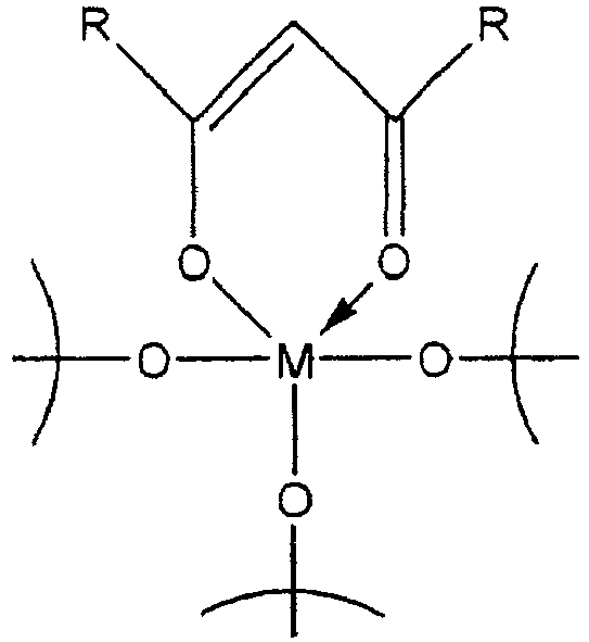

where:M is selected from the group consisting of Ti and Zr; andeach R is individually selected from the group consisting of hydrogen, and branched or unbranched C1-C12 alkyls. - The structure of claim 3, wherein said microelectronic structure is selected from the group consisting of silicon, silicon oxide, silicon nitride, silicon oxynitride, aluminum, tungsten, tungsten silicide, gallium arsenide, germanium, tantalum, tantalum nitrite, and SiGe.
- The structure of claim 3, wherein said leg (30) has a width "W" measured at the greatest distance between said vertical sidewalls (38a,38b) and said horizontal section (32) has a length "L" that is the greatest distance along a plane that is parallel to "W", wherein "W" is 80% or less of "L".
- The structure of claim 3, wherein:said horizontal section (32) has an upper surface (40a);said T-shaped structure (28) has a height "H" defined as the greatest distance from the substrate surface (12) to said upper surface (40a);said leg (30) has a width "W" defined as the greatest distance between said vertical sidewalls (38a,38b); and "H"/"W" is from 2 to 5.
- A method of forming a microelectronic structure according to claim 2, wherein said microelectronic substrate (10) has a surface (12), and optionally one or more intermediate layers on said surface (12), and wherein said applying comprises applying said hard first composition to said substrate surface (12), or to an intermediate layer on said substrate surface (12), to form a hard mask layer (18) thereon,
said method further comprising:optionally forming one or more intermediate layers on said hard mask layer (18);forming an imaging layer (22) on said hard mask layer (18), or on intermediate layers on said hard mask (18);exposing said imaging layer (22) to light to form light-exposed portions of the imaging layer (22);developing said imaging layer (22) after light exposure so as to remove said light-exposed portions, and portions of said hard mask layer (18) adjacent said light-exposed portions, wherein said developing yields a T-shaped structure (28) on said substrate surface (12), or on an intermediate layer on said substrate surface (12), said T-shaped structure (28) comprising:an upright leg (30) having upper and lower portions (34,36) joined by opposing vertical sidewalls (38a,38b) that are perpendicular to said substrate surface (12), said lower portion (36) contacting said substrate surface (12) or intermediate layer and said vertical sidewalls (38a,38b) and substrate surface (12) forming an angle of from 80° to 100°; anda horizontal section (32) being:adjacent said upper portion (34) or an intermediate layer on said upper portion (34); andperpendicular to said vertical sidewalls (38a,38b). - A method of forming a microelectronic structure according to claim 11, wherein said substrate (10) has an etch rate, and said hard mask layer (18) has an etch rate, wherein said hard mask etch rate is at least 3 times said substrate etch rate.
Applications Claiming Priority (3)
| Application Number | Priority Date | Filing Date | Title |
|---|---|---|---|
| US82687506P | 2006-09-25 | 2006-09-25 | |
| US11/858,546 US8168372B2 (en) | 2006-09-25 | 2007-09-20 | Method of creating photolithographic structures with developer-trimmed hard mask |
| PCT/US2007/079217 WO2008039705A1 (en) | 2006-09-25 | 2007-09-21 | Method of creating photolithographic structures with developer-trimmed hard mask |
Publications (3)
| Publication Number | Publication Date |
|---|---|
| EP2089770A1 EP2089770A1 (en) | 2009-08-19 |
| EP2089770A4 EP2089770A4 (en) | 2010-12-15 |
| EP2089770B1 true EP2089770B1 (en) | 2016-06-29 |
Family
ID=39225413
Family Applications (1)
| Application Number | Title | Priority Date | Filing Date |
|---|---|---|---|
| EP07843009.7A Active EP2089770B1 (en) | 2006-09-25 | 2007-09-21 | Method of creating photolithographic structures with developer-trimmed hard mask |
Country Status (7)
| Country | Link |
|---|---|
| US (1) | US8168372B2 (en) |
| EP (1) | EP2089770B1 (en) |
| JP (2) | JP5232155B2 (en) |
| KR (3) | KR101727842B1 (en) |
| CN (1) | CN102520586B (en) |
| TW (1) | TWI440972B (en) |
| WO (1) | WO2008039705A1 (en) |
Families Citing this family (26)
| Publication number | Priority date | Publication date | Assignee | Title |
|---|---|---|---|---|
| JP5357186B2 (en) * | 2008-01-29 | 2013-12-04 | ブルーワー サイエンス アイ エヌ シー. | On-track process for hard mask pattern formation by multiple dark field exposure |
| WO2009132023A2 (en) * | 2008-04-23 | 2009-10-29 | Brewer Science Inc. | Photosensitive hardmask for microlithography |
| US8357617B2 (en) * | 2008-08-22 | 2013-01-22 | Taiwan Semiconductor Manufacturing Company, Ltd. | Method of patterning a metal gate of semiconductor device |
| US9640396B2 (en) | 2009-01-07 | 2017-05-02 | Brewer Science Inc. | Spin-on spacer materials for double- and triple-patterning lithography |
| CN101826457B (en) * | 2009-03-02 | 2012-03-07 | 中芯国际集成电路制造(上海)有限公司 | Production method of grid and MOS transistor |
| KR101311585B1 (en) * | 2010-11-16 | 2013-09-26 | 고려대학교 산학협력단 | Method for fabricating hierarchical superhydrophobic surfaces and superhydrophobic surfaces fabrated by the method |
| JP2014507795A (en) | 2010-12-27 | 2014-03-27 | ブルーワー サイエンス アイ エヌ シー. | Small feature patterning process required for advanced patterning |
| US8568958B2 (en) * | 2011-06-21 | 2013-10-29 | Az Electronic Materials Usa Corp. | Underlayer composition and process thereof |
| US8647809B2 (en) * | 2011-07-07 | 2014-02-11 | Brewer Science Inc. | Metal-oxide films from small molecules for lithographic applications |
| JP5889568B2 (en) | 2011-08-11 | 2016-03-22 | メルク、パテント、ゲゼルシャフト、ミット、ベシュレンクテル、ハフツングMerck Patent GmbH | Composition for forming tungsten oxide film and method for producing tungsten oxide film using the same |
| US8541296B2 (en) * | 2011-09-01 | 2013-09-24 | The Institute of Microelectronics Chinese Academy of Science | Method of manufacturing dummy gates in gate last process |
| CN102983073B (en) * | 2011-09-05 | 2015-12-09 | 中国科学院微电子研究所 | Manufacturing method of small-scale fin structure |
| US9315636B2 (en) | 2012-12-07 | 2016-04-19 | Az Electronic Materials (Luxembourg) S.A.R.L. | Stable metal compounds, their compositions and methods |
| US9102901B2 (en) * | 2012-12-20 | 2015-08-11 | Rohm And Haas Electronic Materials Llc | Methods and compositions for removal of metal hardmasks |
| KR101674989B1 (en) * | 2013-05-21 | 2016-11-22 | 제일모직 주식회사 | Resist underlayer composition, method of forming patterns and semiconductor integrated circuit device including the patterns |
| US9201305B2 (en) | 2013-06-28 | 2015-12-01 | Az Electronic Materials (Luxembourg) S.A.R.L. | Spin-on compositions of soluble metal oxide carboxylates and methods of their use |
| US9296922B2 (en) | 2013-08-30 | 2016-03-29 | Az Electronic Materials (Luxembourg) S.A.R.L. | Stable metal compounds as hardmasks and filling materials, their compositions and methods of use |
| KR102351281B1 (en) * | 2013-09-11 | 2022-01-14 | 제이에스알 가부시끼가이샤 | Composition for forming inorganic film for multilayer resist process, and pattern formation method |
| US9409793B2 (en) | 2014-01-14 | 2016-08-09 | Az Electronic Materials (Luxembourg) S.A.R.L. | Spin coatable metallic hard mask compositions and processes thereof |
| JP6413333B2 (en) * | 2014-05-13 | 2018-10-31 | Jsr株式会社 | Pattern formation method |
| US9499698B2 (en) | 2015-02-11 | 2016-11-22 | Az Electronic Materials (Luxembourg)S.A.R.L. | Metal hardmask composition and processes for forming fine patterns on semiconductor substrates |
| TWI755564B (en) | 2017-09-06 | 2022-02-21 | 德商馬克專利公司 | Spin-on inorganic oxide containing composition, method of manufacturing an electronic device and process of coating a hard mask composition on silicon substrates |
| JPWO2022186231A1 (en) * | 2021-03-03 | 2022-09-09 | ||
| JP2025063613A (en) * | 2023-10-04 | 2025-04-16 | 信越化学工業株式会社 | Composition for forming metal-containing film, pattern forming method |
| CN117936369A (en) * | 2023-12-25 | 2024-04-26 | 中国科学院微电子研究所 | Dual patterning method, semiconductor device and electronic equipment |
| JP2025101957A (en) * | 2023-12-26 | 2025-07-08 | 信越化学工業株式会社 | Metal-containing film-forming compound, metal-containing film-forming composition, pattern forming method |
Citations (1)
| Publication number | Priority date | Publication date | Assignee | Title |
|---|---|---|---|---|
| EP0092782A2 (en) * | 1982-04-22 | 1983-11-02 | E.I. Du Pont De Nemours And Company | Overcoated photohardenable element having surface protuberances |
Family Cites Families (23)
| Publication number | Priority date | Publication date | Assignee | Title |
|---|---|---|---|---|
| JPS58127326A (en) * | 1982-01-26 | 1983-07-29 | Toshiba Corp | Preparation of semiconductor device |
| JP2919004B2 (en) * | 1990-07-12 | 1999-07-12 | 沖電気工業株式会社 | Pattern formation method |
| JP2001071452A (en) * | 1999-07-05 | 2001-03-21 | Fuji Photo Film Co Ltd | Original plate of lithographic printing plate and method for producing lithographic printing plate using the same |
| US6284613B1 (en) * | 1999-11-05 | 2001-09-04 | Chartered Semiconductor Manufacturing Ltd. | Method for forming a T-gate for better salicidation |
| US6630785B1 (en) * | 2000-05-30 | 2003-10-07 | Ritdisplay Corporation | Surface treatment process for fabricating a panel of an organic light emitting device |
| US7008832B1 (en) * | 2000-07-20 | 2006-03-07 | Advanced Micro Devices, Inc. | Damascene process for a T-shaped gate electrode |
| WO2002014954A2 (en) | 2000-08-17 | 2002-02-21 | Shipley Company, L.L.C. | Antireflective coating compositions |
| US6509253B1 (en) * | 2001-02-16 | 2003-01-21 | Advanced Micro Devices, Inc. | T-shaped gate electrode for reduced resistance |
| DE10163557B4 (en) * | 2001-12-21 | 2007-12-06 | Forschungszentrum Jülich GmbH | Transistor-based sensor with specially designed gate electrode for high-sensitivity detection of analytes |
| US6872506B2 (en) | 2002-06-25 | 2005-03-29 | Brewer Science Inc. | Wet-developable anti-reflective compositions |
| US6740469B2 (en) * | 2002-06-25 | 2004-05-25 | Brewer Science Inc. | Developer-soluble metal alkoxide coatings for microelectronic applications |
| KR100512171B1 (en) | 2003-01-24 | 2005-09-02 | 삼성전자주식회사 | Compositon for a bottom layer resist |
| US7364832B2 (en) * | 2003-06-11 | 2008-04-29 | Brewer Science Inc. | Wet developable hard mask in conjunction with thin photoresist for micro photolithography |
| JP4069025B2 (en) | 2003-06-18 | 2008-03-26 | 信越化学工業株式会社 | Resist underlayer film material and pattern forming method |
| US7223517B2 (en) | 2003-08-05 | 2007-05-29 | International Business Machines Corporation | Lithographic antireflective hardmask compositions and uses thereof |
| US7303855B2 (en) | 2003-10-03 | 2007-12-04 | Shin-Etsu Chemical Co., Ltd. | Photoresist undercoat-forming material and patterning process |
| US7064078B2 (en) | 2004-01-30 | 2006-06-20 | Applied Materials | Techniques for the use of amorphous carbon (APF) for various etch and litho integration scheme |
| US7122455B1 (en) | 2004-03-01 | 2006-10-17 | Advanced Micro Devices, Inc. | Patterning with rigid organic under-layer |
| US7271106B2 (en) | 2004-08-31 | 2007-09-18 | Micron Technology, Inc. | Critical dimension control for integrated circuits |
| JP4347209B2 (en) | 2004-12-13 | 2009-10-21 | 東京応化工業株式会社 | Method for forming resist pattern |
| KR100674967B1 (en) | 2005-04-06 | 2007-01-26 | 삼성전자주식회사 | Method for forming photoresist pattern having fine pitch using double patterning method |
| US20070212649A1 (en) | 2006-03-07 | 2007-09-13 | Asml Netherlands B.V. | Method and system for enhanced lithographic patterning |
| US7906275B2 (en) * | 2006-08-31 | 2011-03-15 | Stc.Unm | Self-aligned spatial frequency doubling |
-
2007
- 2007-09-20 US US11/858,546 patent/US8168372B2/en active Active
- 2007-09-21 KR KR1020157014001A patent/KR101727842B1/en active Active
- 2007-09-21 KR KR1020147023449A patent/KR101584927B1/en active Active
- 2007-09-21 CN CN201110460797.XA patent/CN102520586B/en active Active
- 2007-09-21 EP EP07843009.7A patent/EP2089770B1/en active Active
- 2007-09-21 KR KR1020097008244A patent/KR20090077790A/en not_active Ceased
- 2007-09-21 WO PCT/US2007/079217 patent/WO2008039705A1/en not_active Ceased
- 2007-09-21 JP JP2009529417A patent/JP5232155B2/en active Active
- 2007-09-26 TW TW096135713A patent/TWI440972B/en active
-
2012
- 2012-08-14 JP JP2012179714A patent/JP5374626B2/en active Active
Patent Citations (1)
| Publication number | Priority date | Publication date | Assignee | Title |
|---|---|---|---|---|
| EP0092782A2 (en) * | 1982-04-22 | 1983-11-02 | E.I. Du Pont De Nemours And Company | Overcoated photohardenable element having surface protuberances |
Non-Patent Citations (1)
| Title |
|---|
| DUPONT: "DuPont Tyzor Organic Titanates General Brochure", 2001, pages 1 - 11, Retrieved from the Internet <URL:http://snf.stanford.edu/pipermail/specmat/attachments/20050518/4f890d57/attachment-0002.pdf> [retrieved on 20130710] * |
Also Published As
| Publication number | Publication date |
|---|---|
| TWI440972B (en) | 2014-06-11 |
| JP2010504561A (en) | 2010-02-12 |
| EP2089770A1 (en) | 2009-08-19 |
| TW200832056A (en) | 2008-08-01 |
| US20080076064A1 (en) | 2008-03-27 |
| WO2008039705A1 (en) | 2008-04-03 |
| US8168372B2 (en) | 2012-05-01 |
| KR101727842B1 (en) | 2017-04-17 |
| JP5232155B2 (en) | 2013-07-10 |
| EP2089770A4 (en) | 2010-12-15 |
| CN102520586A (en) | 2012-06-27 |
| JP5374626B2 (en) | 2013-12-25 |
| KR101584927B1 (en) | 2016-01-14 |
| CN102520586B (en) | 2014-09-03 |
| KR20140119146A (en) | 2014-10-08 |
| JP2012238026A (en) | 2012-12-06 |
| KR20150067390A (en) | 2015-06-17 |
| KR20090077790A (en) | 2009-07-15 |
Similar Documents
| Publication | Publication Date | Title |
|---|---|---|
| US8168372B2 (en) | Method of creating photolithographic structures with developer-trimmed hard mask | |
| TWI420571B (en) | Method of forming an electronic device | |
| KR101967189B1 (en) | Substrate comprising self-aligned spacers | |
| KR101746017B1 (en) | Methods of forming electronic devices | |
| US7364832B2 (en) | Wet developable hard mask in conjunction with thin photoresist for micro photolithography | |
| US20080305441A1 (en) | Hardmask composition having antirelective properties and method of patterning material on susbstrate using the same | |
| CN101205291A (en) | Hardmask composition, method for forming material layer, and semiconductor integrated circuit device | |
| JPWO2004074938A1 (en) | Lithographic gap fill material forming composition containing acrylic polymer | |
| US6106995A (en) | Antireflective coating material for photoresists | |
| EP2233978B1 (en) | Composition for formation of anti-reflective film, and pattern formation method using the composition | |
| US20060153987A1 (en) | Organic bottom anti-feflective composition and patterning method using the same | |
| KR20050048950A (en) | Organic anti-reflective coating composition and photoresist pattern-forming method using it | |
| KR20260067885A (en) | Semiconductor photoresist composition and method of forming patterns using the composition | |
| KR100611391B1 (en) | Organic diffuse reflection prevention film composition and pattern formation method using same | |
| CN101517485A (en) | Method of forming a lithographic structure using a developer-trimmed hard mask | |
| HK1072814A (en) | Process for producing an image using a first minimum bottom antireflective coating composition | |
| KR20070106213A (en) | Composition for preventing mixing of the interface between the hard mask film and the photoresist film and a method of manufacturing a semiconductor device using the same |
Legal Events
| Date | Code | Title | Description |
|---|---|---|---|
| PUAI | Public reference made under article 153(3) epc to a published international application that has entered the european phase |
Free format text: ORIGINAL CODE: 0009012 |
|
| 17P | Request for examination filed |
Effective date: 20090420 |
|
| AK | Designated contracting states |
Kind code of ref document: A1 Designated state(s): AT BE BG CH CY CZ DE DK EE ES FI FR GB GR HU IE IS IT LI LT LU LV MC MT NL PL PT RO SE SI SK TR |
|
| DAX | Request for extension of the european patent (deleted) | ||
| A4 | Supplementary search report drawn up and despatched |
Effective date: 20101111 |
|
| 17Q | First examination report despatched |
Effective date: 20110907 |
|
| GRAP | Despatch of communication of intention to grant a patent |
Free format text: ORIGINAL CODE: EPIDOSNIGR1 |
|
| INTG | Intention to grant announced |
Effective date: 20160201 |
|
| GRAS | Grant fee paid |
Free format text: ORIGINAL CODE: EPIDOSNIGR3 |
|
| GRAA | (expected) grant |
Free format text: ORIGINAL CODE: 0009210 |
|
| AK | Designated contracting states |
Kind code of ref document: B1 Designated state(s): AT BE BG CH CY CZ DE DK EE ES FI FR GB GR HU IE IS IT LI LT LU LV MC MT NL PL PT RO SE SI SK TR |
|
| REG | Reference to a national code |
Ref country code: GB Ref legal event code: FG4D |
|
| REG | Reference to a national code |
Ref country code: CH Ref legal event code: EP |
|
| REG | Reference to a national code |
Ref country code: AT Ref legal event code: REF Ref document number: 809562 Country of ref document: AT Kind code of ref document: T Effective date: 20160715 |
|
| REG | Reference to a national code |
Ref country code: IE Ref legal event code: FG4D |
|
| REG | Reference to a national code |
Ref country code: DE Ref legal event code: R096 Ref document number: 602007046829 Country of ref document: DE |
|
| REG | Reference to a national code |
Ref country code: FR Ref legal event code: PLFP Year of fee payment: 10 |
|
| REG | Reference to a national code |
Ref country code: LT Ref legal event code: MG4D |
|
| PG25 | Lapsed in a contracting state [announced via postgrant information from national office to epo] |
Ref country code: LT Free format text: LAPSE BECAUSE OF FAILURE TO SUBMIT A TRANSLATION OF THE DESCRIPTION OR TO PAY THE FEE WITHIN THE PRESCRIBED TIME-LIMIT Effective date: 20160629 Ref country code: FI Free format text: LAPSE BECAUSE OF FAILURE TO SUBMIT A TRANSLATION OF THE DESCRIPTION OR TO PAY THE FEE WITHIN THE PRESCRIBED TIME-LIMIT Effective date: 20160629 |
|
| REG | Reference to a national code |
Ref country code: NL Ref legal event code: MP Effective date: 20160629 |
|
| PG25 | Lapsed in a contracting state [announced via postgrant information from national office to epo] |
Ref country code: SE Free format text: LAPSE BECAUSE OF FAILURE TO SUBMIT A TRANSLATION OF THE DESCRIPTION OR TO PAY THE FEE WITHIN THE PRESCRIBED TIME-LIMIT Effective date: 20160629 Ref country code: GR Free format text: LAPSE BECAUSE OF FAILURE TO SUBMIT A TRANSLATION OF THE DESCRIPTION OR TO PAY THE FEE WITHIN THE PRESCRIBED TIME-LIMIT Effective date: 20160930 Ref country code: NL Free format text: LAPSE BECAUSE OF FAILURE TO SUBMIT A TRANSLATION OF THE DESCRIPTION OR TO PAY THE FEE WITHIN THE PRESCRIBED TIME-LIMIT Effective date: 20160629 Ref country code: LV Free format text: LAPSE BECAUSE OF FAILURE TO SUBMIT A TRANSLATION OF THE DESCRIPTION OR TO PAY THE FEE WITHIN THE PRESCRIBED TIME-LIMIT Effective date: 20160629 |
|
| REG | Reference to a national code |
Ref country code: AT Ref legal event code: MK05 Ref document number: 809562 Country of ref document: AT Kind code of ref document: T Effective date: 20160629 |
|
| PG25 | Lapsed in a contracting state [announced via postgrant information from national office to epo] |
Ref country code: SK Free format text: LAPSE BECAUSE OF FAILURE TO SUBMIT A TRANSLATION OF THE DESCRIPTION OR TO PAY THE FEE WITHIN THE PRESCRIBED TIME-LIMIT Effective date: 20160629 Ref country code: CZ Free format text: LAPSE BECAUSE OF FAILURE TO SUBMIT A TRANSLATION OF THE DESCRIPTION OR TO PAY THE FEE WITHIN THE PRESCRIBED TIME-LIMIT Effective date: 20160629 Ref country code: EE Free format text: LAPSE BECAUSE OF FAILURE TO SUBMIT A TRANSLATION OF THE DESCRIPTION OR TO PAY THE FEE WITHIN THE PRESCRIBED TIME-LIMIT Effective date: 20160629 Ref country code: IS Free format text: LAPSE BECAUSE OF FAILURE TO SUBMIT A TRANSLATION OF THE DESCRIPTION OR TO PAY THE FEE WITHIN THE PRESCRIBED TIME-LIMIT Effective date: 20161029 Ref country code: RO Free format text: LAPSE BECAUSE OF FAILURE TO SUBMIT A TRANSLATION OF THE DESCRIPTION OR TO PAY THE FEE WITHIN THE PRESCRIBED TIME-LIMIT Effective date: 20160629 Ref country code: IT Free format text: LAPSE BECAUSE OF FAILURE TO SUBMIT A TRANSLATION OF THE DESCRIPTION OR TO PAY THE FEE WITHIN THE PRESCRIBED TIME-LIMIT Effective date: 20160629 |
|
| PG25 | Lapsed in a contracting state [announced via postgrant information from national office to epo] |
Ref country code: BE Free format text: LAPSE BECAUSE OF NON-PAYMENT OF DUE FEES Effective date: 20160629 Ref country code: AT Free format text: LAPSE BECAUSE OF FAILURE TO SUBMIT A TRANSLATION OF THE DESCRIPTION OR TO PAY THE FEE WITHIN THE PRESCRIBED TIME-LIMIT Effective date: 20160629 Ref country code: PL Free format text: LAPSE BECAUSE OF FAILURE TO SUBMIT A TRANSLATION OF THE DESCRIPTION OR TO PAY THE FEE WITHIN THE PRESCRIBED TIME-LIMIT Effective date: 20160629 Ref country code: PT Free format text: LAPSE BECAUSE OF FAILURE TO SUBMIT A TRANSLATION OF THE DESCRIPTION OR TO PAY THE FEE WITHIN THE PRESCRIBED TIME-LIMIT Effective date: 20161031 Ref country code: ES Free format text: LAPSE BECAUSE OF FAILURE TO SUBMIT A TRANSLATION OF THE DESCRIPTION OR TO PAY THE FEE WITHIN THE PRESCRIBED TIME-LIMIT Effective date: 20160629 |
|
| REG | Reference to a national code |
Ref country code: DE Ref legal event code: R097 Ref document number: 602007046829 Country of ref document: DE |
|
| PG25 | Lapsed in a contracting state [announced via postgrant information from national office to epo] |
Ref country code: MC Free format text: LAPSE BECAUSE OF FAILURE TO SUBMIT A TRANSLATION OF THE DESCRIPTION OR TO PAY THE FEE WITHIN THE PRESCRIBED TIME-LIMIT Effective date: 20160629 |
|
| REG | Reference to a national code |
Ref country code: CH Ref legal event code: PL |
|
| PLBE | No opposition filed within time limit |
Free format text: ORIGINAL CODE: 0009261 |
|
| STAA | Information on the status of an ep patent application or granted ep patent |
Free format text: STATUS: NO OPPOSITION FILED WITHIN TIME LIMIT |
|
| PG25 | Lapsed in a contracting state [announced via postgrant information from national office to epo] |
Ref country code: DK Free format text: LAPSE BECAUSE OF FAILURE TO SUBMIT A TRANSLATION OF THE DESCRIPTION OR TO PAY THE FEE WITHIN THE PRESCRIBED TIME-LIMIT Effective date: 20160629 |
|
| 26N | No opposition filed |
Effective date: 20170330 |
|
| REG | Reference to a national code |
Ref country code: IE Ref legal event code: MM4A |
|
| PG25 | Lapsed in a contracting state [announced via postgrant information from national office to epo] |
Ref country code: CH Free format text: LAPSE BECAUSE OF NON-PAYMENT OF DUE FEES Effective date: 20160930 Ref country code: IE Free format text: LAPSE BECAUSE OF NON-PAYMENT OF DUE FEES Effective date: 20160921 Ref country code: LI Free format text: LAPSE BECAUSE OF NON-PAYMENT OF DUE FEES Effective date: 20160930 |
|
| PG25 | Lapsed in a contracting state [announced via postgrant information from national office to epo] |
Ref country code: SI Free format text: LAPSE BECAUSE OF FAILURE TO SUBMIT A TRANSLATION OF THE DESCRIPTION OR TO PAY THE FEE WITHIN THE PRESCRIBED TIME-LIMIT Effective date: 20160629 Ref country code: BG Free format text: LAPSE BECAUSE OF FAILURE TO SUBMIT A TRANSLATION OF THE DESCRIPTION OR TO PAY THE FEE WITHIN THE PRESCRIBED TIME-LIMIT Effective date: 20160929 Ref country code: LU Free format text: LAPSE BECAUSE OF NON-PAYMENT OF DUE FEES Effective date: 20160921 |
|
| REG | Reference to a national code |
Ref country code: FR Ref legal event code: PLFP Year of fee payment: 11 |
|
| PG25 | Lapsed in a contracting state [announced via postgrant information from national office to epo] |
Ref country code: HU Free format text: LAPSE BECAUSE OF FAILURE TO SUBMIT A TRANSLATION OF THE DESCRIPTION OR TO PAY THE FEE WITHIN THE PRESCRIBED TIME-LIMIT; INVALID AB INITIO Effective date: 20070921 Ref country code: CY Free format text: LAPSE BECAUSE OF FAILURE TO SUBMIT A TRANSLATION OF THE DESCRIPTION OR TO PAY THE FEE WITHIN THE PRESCRIBED TIME-LIMIT Effective date: 20160629 |
|
| PG25 | Lapsed in a contracting state [announced via postgrant information from national office to epo] |
Ref country code: MT Free format text: LAPSE BECAUSE OF NON-PAYMENT OF DUE FEES Effective date: 20160930 Ref country code: TR Free format text: LAPSE BECAUSE OF FAILURE TO SUBMIT A TRANSLATION OF THE DESCRIPTION OR TO PAY THE FEE WITHIN THE PRESCRIBED TIME-LIMIT Effective date: 20160629 |
|
| REG | Reference to a national code |
Ref country code: FR Ref legal event code: PLFP Year of fee payment: 12 |
|
| REG | Reference to a national code |
Ref country code: DE Ref legal event code: R119 Ref document number: 602007046829 Country of ref document: DE |
|
| PG25 | Lapsed in a contracting state [announced via postgrant information from national office to epo] |
Ref country code: DE Free format text: LAPSE BECAUSE OF NON-PAYMENT OF DUE FEES Effective date: 20200401 |
|
| PGFP | Annual fee paid to national office [announced via postgrant information from national office to epo] |
Ref country code: GB Payment date: 20240927 Year of fee payment: 18 |
|
| PGFP | Annual fee paid to national office [announced via postgrant information from national office to epo] |
Ref country code: FR Payment date: 20250925 Year of fee payment: 19 |