EP2086157A1 - Method and device for processing data and communication system comprising such device - Google Patents
Method and device for processing data and communication system comprising such device Download PDFInfo
- Publication number
- EP2086157A1 EP2086157A1 EP08001750A EP08001750A EP2086157A1 EP 2086157 A1 EP2086157 A1 EP 2086157A1 EP 08001750 A EP08001750 A EP 08001750A EP 08001750 A EP08001750 A EP 08001750A EP 2086157 A1 EP2086157 A1 EP 2086157A1
- Authority
- EP
- European Patent Office
- Prior art keywords
- control parameter
- data
- digital
- histogram
- signal
- Prior art date
- Legal status (The legal status is an assumption and is not a legal conclusion. Google has not performed a legal analysis and makes no representation as to the accuracy of the status listed.)
- Granted
Links
Images



Classifications
-
- H—ELECTRICITY
- H04—ELECTRIC COMMUNICATION TECHNIQUE
- H04L—TRANSMISSION OF DIGITAL INFORMATION, e.g. TELEGRAPHIC COMMUNICATION
- H04L7/00—Arrangements for synchronising receiver with transmitter
- H04L7/0054—Detection of the synchronisation error by features other than the received signal transition
-
- H—ELECTRICITY
- H04—ELECTRIC COMMUNICATION TECHNIQUE
- H04L—TRANSMISSION OF DIGITAL INFORMATION, e.g. TELEGRAPHIC COMMUNICATION
- H04L7/00—Arrangements for synchronising receiver with transmitter
- H04L7/02—Speed or phase control by the received code signals, the signals containing no special synchronisation information
- H04L7/033—Speed or phase control by the received code signals, the signals containing no special synchronisation information using the transitions of the received signal to control the phase of the synchronising-signal-generating means, e.g. using a phase-locked loop
- H04L7/0331—Speed or phase control by the received code signals, the signals containing no special synchronisation information using the transitions of the received signal to control the phase of the synchronising-signal-generating means, e.g. using a phase-locked loop with a digital phase-locked loop [PLL] processing binary samples, e.g. add/subtract logic for correction of receiver clock
Definitions
- the invention relates to a method and to a device for processing data and to a communication system comprising such a device.
- optical communication requires high order modulation, e.g., 100Gbit/s PolMUX-QPSK (polarization multiplex quaternary phase shift keying) employing both polarizations and complex signal constellations in each polarization for information transport.
- CD chromatic dispersion
- PMD polarization mode dispersion
- Fig.1 shows a exemplary setup of a system providing coherent demodulation of optical communications signals.
- An optical transmission line 101 is fed to a coherent optical front end comprising a free running local oscillator ("90°-hybrid") 102, the output of which is processed by an analog/digital-converter 103 providing a sampled and quantized representation of the optical field as an electrical receive signal.
- Said signal may comprise statistic noise distortions and deterministic channel distortions.
- the latter can be compensated by an equalizer 105.
- a clock recovery 104 tracks and corrects phase and frequency offsets between the transmitter's and the receiver's symbol clocks.
- the clock recovery 104 has a feedback loop towards the analog/digital-converter 103.
- a phase recovery 106 is deployed subsequent to the equalization 105 and the output of the phase recovery 106 is fed to a detection unit 107 for processing/detecting the signal received.
- the signal processing including the clock recovery 104, the equalization 105, the phase recovery 106 and the detection 107, preferably processes digital signals, i.e. subsequent to the analog/digital-converter 103 the receiver processes digital data.
- processing digital data requires a significant high processing speed at the receiver based on the symbol rate of the optical data received. According to such high requirements towards processing speed, digital data at the receiver may preferably be processed by methods of limited or low complexity.
- the problem to be solved is to overcome the disadvantages as stated before and in particular to provide signal recovery, in particular timing and/or clock recovery, that is robust against any kind of distortion and that is fast enough to track time varying clocking disturbances. Furthermore, the clock recovery should be able to cope with a 2-fold over-sampling input of the analog/digital-converter, wherein such input implies that the analog/digital-converter provides two digital samples per symbol.
- a symbol may in particular be any information conveyed and/or associated with the data.
- a symbol may be associated with a modulation technique conveying information via symbols, e.g., predetermined coordinates within constellation diagrams (as, e.g., in quadrature amplitude modulation).
- control parameter can be evaluated based on the correlation property of the symbols.
- the correlation property may in particular be associated with a symmetry criterion.
- the approach provided allows an implementation complexity in particular of a (digital) receiver enabling high processing speed. It may be operated at a sampling rate of two samples per symbol and it may require no further up-sampling or interpolation.
- the approach suggested is robust against channel distortions and sufficiently fast to track and/or compensate clocking disturbances.
- Data may comprise any kind of signal or data to be provided from a component or element directly or indirectly via a fixed line or a radio interface or connection.
- the data may in particular be digital data provided, e.g., by an analog/digital-converter.
- a phase of the data is modified pursuant to the control parameter.
- the phase may be shifted in order to obtain a more balanced correlation.
- the phase of the data is modified by controlling a sampling phase via said control parameter.
- Said sampling phase may be controlled by shifting the sampling phase of an analog/digital-converter by shifting the sampling phase of an interpolator that is preferably arranged subsequent to the analog/digital-converter.
- phase of the data is modified by controlling an interpolator or an interpolation via said control parameter.
- the data is processed to detect a signal, in particular a timing signal or a clock signal.
- the approach may in particular be used for clock recovery applications in a receiver.
- the input signal is a digital signal, in particular a signal provided by an analog/digital-converter.
- the input signal comprises at least two samples per symbol.
- the correlation property of the symbols is based on a histogram.
- the control parameter may be determined based on at least one symmetry property of said histogram.
- the histogram can be a matrix. It is further possible that the histogram or the matrix or portions thereof are weighted or filtered in order to bring out relevant portions. This may result in an improved controlling.
- control parameter is determined in order to improve the at least one symmetry property of said histogram.
- an iterative evaluation may apply in order to subsequently obtain (and hence provide) an improved (or optimized) value for the control parameter.
- control parameter is determined based on a data block.
- the data block may comprise a predetermined number of symbols.
- a given length of said data block (input signal) may be used, e.g., to obtain a clock signal or to synchronize on said clock signal, i.e. for clock-recovery purposes.
- the approach may be used in a digital radio or mobile communication.
- a device for data processing comprising a processor unit and/or a hard-wired circuit (e.g., an ASIC or an FPGA) that is equipped and/or arranged such that the method as described herein is executable thereon.
- a hard-wired circuit e.g., an ASIC or an FPGA
- the device is a communication device, in particular a receiver of an optical communication system.
- the communication system may in particular be an optical communication system.
- a correlation between two adjacent symbols is evaluated within a block of a digital input signal comprising several samples.
- Such block of samples can be determined to have a given length in order to, e.g., recover a timing information, in particular a clock signal.
- the block may be of a fixed length or it can be of variable length depending on the signal recovery itself: E.g., if the signal (clock) could be determined with a predetermined certainty, the process of recovery may end.
- Correlation properties could be read, e.g., from a 2-dimensional histogram. From symmetry properties of such histogram, a control parameter can be derived, which relates to the sampling phase. This control parameter can either control the sampling phase of an analog/digital-converter providing the samples or it may control an interpolator.
- the signal recovery in particular timing information recovery and/or clock recovery suggested may be applied in any digital communication system, e.g., mobile or radio communication. It may in particular be used in high speed transmission systems, e.g., in electrical receivers of optical (ultra) long haul and/or metro communication systems where blind timing phase estimation is required.
- the input signal fed to the clock recovery is the digital sequence from the analog/digital-converter (see Fig.1 ). Such input signal can be referred to as data processed according to this approach.
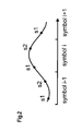
- every symbol may be represented by two (substantially) equally spaced samples s1 and s2 (see Fig.2 and Fig.3 ). Each symbol has a duration of T, which leads to a distance of T/2 between two adjacent samples.
- the distance between samples that is used for the axis of the histogram can differ from T/2. Such distance may in particular amount to kT/2 (k being a natural number). Hence, samples do not have to be adjacent to one another.
- a running mean may be determined across n even and odd samples symmetrically around the symbol to be determined, wherein n is proportional to a number of predecessor samples as well as successor samples.
- a histogram is generated, where the values of the first sample s1 are aligned with the x-axis and the values of s2 are aligned with the y-axis, spanning a 2-dimensional coordinate system.
- the length of the according axes may be defined by a number of quantization steps of the analog/digital-converter.
- the relative frequency represents a common probability density function (PDF) of the amplitude distribution of both samples s1 and s2.
- PDF probability density function
- Fig.2 shows samples S1 and S2 at a sampling phase of [T/4; 3T/4] and Fig.3 shows samples S1 and S2 at a sampling phase of [0; T/2].
- both samples S1 and S2 show similar amplitude values.
- a resulting histogram is substantially symmetric to the line of origin between both axes.
- the samples s2 show substantially minimum and maximum values and the samples s1 show values in between these extreme values.
- FIG.4 depicting a symmetry to the line of origin 401.
- FIG.5 A corresponding histogram of asymmetric shape for the sampling phase [0; T/2] according to Fig.3 is shown in Fig.5 .
- This histogram shows a stronger weight 502 in the left half plane.
- a resulting control parameter may indicate an early sampling phase.
- Fig.5 comprises a line of origin 501.
- the according histogram becomes asymmetric, which leads to the desired control parameter indicating to modify the phase in order to reach the symmetric case (again).
- this technique is robust against strong channel impairment, noise, interference and/or distortion.
- a control parameter may be determined by comparing two bins of the histogram with a symmetric position in respect to the line of origin. A difference of the likelihood of both bins may be determined and all such differences in the histogram can be accumulated in order to obtain the control parameter, that detects by its sign whether the weight of the histogram is shifted to the left (negative sign) or to the right (positive sign) half plane. This corresponds to an early or late sampling phase.
- the bin mentioned may refer to a 2-dimensional field determined by the quantization range of the analog/digital-converter providing samples of certain values.
- control parameter R In case of a histogram weight tends towards the left half plane, the control parameter R is below 0 (see Fig.5 ) and the control parameter R is above 0 for a weight towards the right half plane.
- Fig.6 shows an exemplary function of the control parameter R depending on a sampling phase for a symbol duration of 30ps.
- the function shows a stable operating point for the balanced sampling phase of [T/4; 3T/4].
- control parameter may directly drive the sampling phase in the analog/digital-converter without any additional measure. In case a subsequent equalization needs a different sampling value, this could be achieved by a digital interpolator, which shifts the received data to the desired sampling phase.
- a feedback-based timing recovery is depicted in Fig.7A comprising an analog/digital-converter ADC 701 providing an output to a Timing Error Detector 702 that feeds back a control parameter to the analog/digital-converter ADC 701.
- control parameter R can also be used to control an interpolator 704 in a feed forward structure, leaving an analog/digital-converter ADC 703 unaffected.
- the output signal provided by the analog/digital-converter ADC 703 is fed to the Interpolator 704 and to a Timing Error Detector 705, wherein the Timing Error Detector 705 forwards said control parameter to the Interpolator 704.
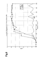
- the approach suggested allows significant improved results compared to known technologies as is shown an exemplary graph according to Fig.8 for 111Gbit/s PolMux QPSK.
- the various graphs show a phase deviation (y-axis) in view of a dispersion (in ps/nm).
- a graph 801 depicts the result that is obtained by the approach presented herein.
- the approach suggested can be realized based on simple mathematical operations like binary additions, which allow a reduced implementation complexity and therefore applications to be run at a high processing speed within the receiver. Furthermore, block-wise processing allows a high degree of parallelization, which even enables an implementation in FPGAs.
- the solution described may be implemented, e.g., in an ASIC, FPGA or in a device utilizing such or a similar technology.
- the technology can be used in receivers with coherent demodulation at high data rates in optical communication systems with digital signal processing at the receiver for equalization purposes utilizing, e.g., 100Gbit/s PolMUX-QPSK (25GBaud) systems.
- the utilization of the concept provided is not limited to optical communication systems or to coherent demodulation. It may in particular be applied to any digital communication system.
Landscapes
- Engineering & Computer Science (AREA)
- Computer Networks & Wireless Communication (AREA)
- Signal Processing (AREA)
- Synchronisation In Digital Transmission Systems (AREA)
- Optical Communication System (AREA)
Abstract
Description
- The invention relates to a method and to a device for processing data and to a communication system comprising such a device.
- To increase the bandwidth efficiency and robustness against distortions, optical communication requires high order modulation, e.g., 100Gbit/s PolMUX-QPSK (polarization multiplex quaternary phase shift keying) employing both polarizations and complex signal constellations in each polarization for information transport. Such modulation of high order allows a reduction of the symbol rate to
100GBit/s : 4 = 25GBit/s,
which increases a robustness against optical distortions like chromatic dispersion (CD) or polarization mode dispersion (PMD). This approach also reduces performance requirements towards the hardware for electrical post processing in the receiver. -
Fig.1 shows a exemplary setup of a system providing coherent demodulation of optical communications signals. - An
optical transmission line 101 is fed to a coherent optical front end comprising a free running local oscillator ("90°-hybrid") 102, the output of which is processed by an analog/digital-converter 103 providing a sampled and quantized representation of the optical field as an electrical receive signal. Said signal may comprise statistic noise distortions and deterministic channel distortions. The latter can be compensated by anequalizer 105. Aclock recovery 104 tracks and corrects phase and frequency offsets between the transmitter's and the receiver's symbol clocks. - The
clock recovery 104 has a feedback loop towards the analog/digital-converter 103. Aphase recovery 106 is deployed subsequent to theequalization 105 and the output of thephase recovery 106 is fed to adetection unit 107 for processing/detecting the signal received. - For economic reasons, the signal processing including the
clock recovery 104, theequalization 105, thephase recovery 106 and thedetection 107, preferably processes digital signals, i.e. subsequent to the analog/digital-converter 103 the receiver processes digital data. However, processing digital data requires a significant high processing speed at the receiver based on the symbol rate of the optical data received. According to such high requirements towards processing speed, digital data at the receiver may preferably be processed by methods of limited or low complexity. - The problem to be solved is to overcome the disadvantages as stated before and in particular to provide signal recovery, in particular timing and/or clock recovery, that is robust against any kind of distortion and that is fast enough to track time varying clocking disturbances. Furthermore, the clock recovery should be able to cope with a 2-fold over-sampling input of the analog/digital-converter, wherein such input implies that the analog/digital-converter provides two digital samples per symbol.
- This problem is solved according to the features of the independent claims. Further embodiments result from the depending claims.
- In order to overcome this problem, a method for processing data is provided
- wherein said data comprises symbols;
- wherein a control parameter is determined based on a correlation property of the symbols of said data.
- It is to be noted that a symbol may in particular be any information conveyed and/or associated with the data. A symbol may be associated with a modulation technique conveying information via symbols, e.g., predetermined coordinates within constellation diagrams (as, e.g., in quadrature amplitude modulation).
- Advantageously, said control parameter can be evaluated based on the correlation property of the symbols.
- The correlation property may in particular be associated with a symmetry criterion.
- The approach provided allows an implementation complexity in particular of a (digital) receiver enabling high processing speed. It may be operated at a sampling rate of two samples per symbol and it may require no further up-sampling or interpolation.
- Further, the approach suggested is robust against channel distortions and sufficiently fast to track and/or compensate clocking disturbances.
- Data may comprise any kind of signal or data to be provided from a component or element directly or indirectly via a fixed line or a radio interface or connection. The data may in particular be digital data provided, e.g., by an analog/digital-converter.
- In an embodiment, a phase of the data is modified pursuant to the control parameter.
- Hence, the phase may be shifted in order to obtain a more balanced correlation.
- In another embodiment, the phase of the data is modified by controlling a sampling phase via said control parameter.
- Said sampling phase may be controlled by shifting the sampling phase of an analog/digital-converter by shifting the sampling phase of an interpolator that is preferably arranged subsequent to the analog/digital-converter.
- In a further embodiment, the phase of the data is modified by controlling an interpolator or an interpolation via said control parameter.
- In a next embodiment, the data is processed to detect a signal, in particular a timing signal or a clock signal.
- The approach may in particular be used for clock recovery applications in a receiver.
- It is also an embodiment that the input signal is a digital signal, in particular a signal provided by an analog/digital-converter.
- Pursuant to another embodiment, the input signal comprises at least two samples per symbol.
- According to an embodiment, the correlation property of the symbols is based on a histogram. Preferably, the control parameter may be determined based on at least one symmetry property of said histogram.
- The histogram can be a matrix. It is further possible that the histogram or the matrix or portions thereof are weighted or filtered in order to bring out relevant portions. This may result in an improved controlling.
- According to another embodiment, the control parameter is determined in order to improve the at least one symmetry property of said histogram.
- Hence, an iterative evaluation may apply in order to subsequently obtain (and hence provide) an improved (or optimized) value for the control parameter.
- In yet another embodiment, the control parameter is determined according to

wherein - R
- denotes the control parameter;
- q
- denotes a number of quantization bins;
- H(i,j)
- refers to a bin in the histogram with coordinates defined by a line i and a column j.
- According to a next embodiment, the control parameter is determined based on a data block. The data block may comprise a predetermined number of symbols.
- Hence a given length of said data block (input signal) may be used, e.g., to obtain a clock signal or to synchronize on said clock signal, i.e. for clock-recovery purposes.
- Pursuant to yet an embodiment, the approach may be used in a digital radio or mobile communication.
- The problem stated above is also solved by a device for data processing comprising a processor unit and/or a hard-wired circuit (e.g., an ASIC or an FPGA) that is equipped and/or arranged such that the method as described herein is executable thereon.
- According to an embodiment, the device is a communication device, in particular a receiver of an optical communication system.
- The problem stated supra is further solved by a communication system comprising the device as described herein.
- The communication system may in particular be an optical communication system.
- Embodiments of the invention are shown and illustrated in the following figures:
- Fig.2
- shows a sampling of an analogue receive signal in an analog/digital-converter for sampling points at [T/4; 3T/4];
- Fig.3
- shows a sampling of an analogue receive signal in an analog/digital-converter for sampling points at [0; T/2];
- Fig.4
- shows a histogram according to the example shown in
Fig.2 ; - Fig.5
- shows a histogram according to the example shown in
Fig.3 ; - Fig.6
- shows an exemplary function of the control parameter R depending on a sampling phase for a symbol duration of 30ps, wherein said function shows a stable operating point for the balanced sampling phase of [T/4; 3T/4];
- Fig.7A
- shows how the control parameter can be utilized in a feedback structure for timing recovery purposes;
- Fig.7B
- shows how the control parameter can be utilized in a feed forward structure for timing recovery purposes;
- Fig.8
- shows exemplary graphs comparing the approach presented herein with other schemes, pointing out a phase deviation over a chromatic dispersion.
- For an exemplary sampling rate of 2 samples per symbol, a correlation between two adjacent symbols is evaluated within a block of a digital input signal comprising several samples. Such block of samples can be determined to have a given length in order to, e.g., recover a timing information, in particular a clock signal. The block may be of a fixed length or it can be of variable length depending on the signal recovery itself: E.g., if the signal (clock) could be determined with a predetermined certainty, the process of recovery may end.
- Correlation properties could be read, e.g., from a 2-dimensional histogram. From symmetry properties of such histogram, a control parameter can be derived, which relates to the sampling phase. This control parameter can either control the sampling phase of an analog/digital-converter providing the samples or it may control an interpolator.
- For the approach provided herein, advantageously the following requirements and/or options are met or fulfilled:
- (1) The sampling rate amounts to at least 2 samples per symbol.
- (2) The number of samples per evaluated block is preferably larger than 2. Larger blocks lead to improved sampling phase estimations, especially in presence of strong signal distortions.
- (3) Correlation properties may be evaluated with or without building up or utilization of a histogram.
- (4) Histograms with higher orders than
dimension 2 may be utilized. - The signal recovery, in particular timing information recovery and/or clock recovery suggested may be applied in any digital communication system, e.g., mobile or radio communication. It may in particular be used in high speed transmission systems, e.g., in electrical receivers of optical (ultra) long haul and/or metro communication systems where blind timing phase estimation is required.
- The input signal fed to the clock recovery is the digital sequence from the analog/digital-converter (see
Fig.1 ). Such input signal can be referred to as data processed according to this approach. - At 2-fold over-sampling, every symbol may be represented by two (substantially) equally spaced samples s1 and s2 (see
Fig.2 andFig.3 ). Each symbol has a duration of T, which leads to a distance of T/2 between two adjacent samples. - It is noted that the distance between samples that is used for the axis of the histogram can differ from T/2. Such distance may in particular amount to kT/2 (k being a natural number). Hence, samples do not have to be adjacent to one another.
- It is an option to pre-process the samples, e.g., filtering, weighting, processing mean values, cumulating samples. In particular, a running mean may be determined across n even and odd samples symmetrically around the symbol to be determined, wherein n is proportional to a number of predecessor samples as well as successor samples.
- From a data block comprising a sufficient amount of N digital samples (N is a multiple of the over-sampling factor), a histogram is generated, where the values of the first sample s1 are aligned with the x-axis and the values of s2 are aligned with the y-axis, spanning a 2-dimensional coordinate system. The length of the according axes may be defined by a number of quantization steps of the analog/digital-converter.
- For every pair of samples (s1,s2) the relative frequency of occurrence within the data block is evaluated. The relative frequency represents a common probability density function (PDF) of the amplitude distribution of both samples s1 and s2.
-
Fig.2 shows samples S1 and S2 at a sampling phase of [T/4; 3T/4] andFig.3 shows samples S1 and S2 at a sampling phase of [0; T/2]. - According to the example shown in
Fig.2 , both samples S1 and S2 show similar amplitude values. Hence, a resulting histogram is substantially symmetric to the line of origin between both axes. - According to the example shown in
Fig.3 , the samples s2 show substantially minimum and maximum values and the samples s1 show values in between these extreme values. - A corresponding histogram for the sampling phase [T/4; 3T/4] according to
Fig.2 is shown inFig.4 depicting a symmetry to the line oforigin 401. - A corresponding histogram of asymmetric shape for the sampling phase [0; T/2] according to
Fig.3 is shown inFig.5 . This histogram shows astronger weight 502 in the left half plane. Hence, a resulting control parameter may indicate an early sampling phase. Similar toFig.4 ,Fig.5 comprises a line oforigin 501. - Because dominant deterministic channel distortions like chromatic dispersion are substantially symmetric with respect to the pulse centre (raising flank exhibits same distortion as falling flank), the resulting histogram inherits a symmetric shape for balanced sampling points with respect to the pulse centre. Hence, even when strong distortions are present, a symmetric shape may arise in the case of the sampling phase set to [T/4; 3T/4].
- In case of an early or late sampling phase, the according histogram becomes asymmetric, which leads to the desired control parameter indicating to modify the phase in order to reach the symmetric case (again). Hence, this technique is robust against strong channel impairment, noise, interference and/or distortion.
- A control parameter may be determined by comparing two bins of the histogram with a symmetric position in respect to the line of origin. A difference of the likelihood of both bins may be determined and all such differences in the histogram can be accumulated in order to obtain the control parameter, that detects by its sign whether the weight of the histogram is shifted to the left (negative sign) or to the right (positive sign) half plane. This corresponds to an early or late sampling phase.
- The bin mentioned may refer to a 2-dimensional field determined by the quantization range of the analog/digital-converter providing samples of certain values.
- In particular, the control parameter may be calculated as follows:

where - q
- denotes a number of quantization bins,
- H(i,j)
- refers to a bin in the histogram with coordinates defined by line i and column j.
- In case of a histogram weight tends towards the left half plane, the control parameter R is below 0 (see
Fig.5 ) and the control parameter R is above 0 for a weight towards the right half plane. -
Fig.6 shows an exemplary function of the control parameter R depending on a sampling phase for a symbol duration of 30ps. - The function shows a stable operating point for the balanced sampling phase of [T/4; 3T/4].
- If a balanced sampling phase is required, the control parameter may directly drive the sampling phase in the analog/digital-converter without any additional measure. In case a subsequent equalization needs a different sampling value, this could be achieved by a digital interpolator, which shifts the received data to the desired sampling phase. A feedback-based timing recovery is depicted in
Fig.7A comprising an analog/digital-converter ADC 701 providing an output to aTiming Error Detector 702 that feeds back a control parameter to the analog/digital-converter ADC 701. - As shown in
Fig.7B , the control parameter R can also be used to control aninterpolator 704 in a feed forward structure, leaving an analog/digital-converter ADC 703 unaffected. InFig.7B the output signal provided by the analog/digital-converter ADC 703 is fed to theInterpolator 704 and to aTiming Error Detector 705, wherein theTiming Error Detector 705 forwards said control parameter to theInterpolator 704. - Advantageously, the approach suggested allows significant improved results compared to known technologies as is shown an exemplary graph according to
Fig.8 for 111Gbit/s PolMux QPSK. - The various graphs show a phase deviation (y-axis) in view of a dispersion (in ps/nm). A
graph 801 depicts the result that is obtained by the approach presented herein. - Advantageously, the approach suggested can be realized based on simple mathematical operations like binary additions, which allow a reduced implementation complexity and therefore applications to be run at a high processing speed within the receiver. Furthermore, block-wise processing allows a high degree of parallelization, which even enables an implementation in FPGAs.
- Hence, the solution described may be implemented, e.g., in an ASIC, FPGA or in a device utilizing such or a similar technology.
- The technology can be used in receivers with coherent demodulation at high data rates in optical communication systems with digital signal processing at the receiver for equalization purposes utilizing, e.g., 100Gbit/s PolMUX-QPSK (25GBaud) systems.
- The utilization of the concept provided is not limited to optical communication systems or to coherent demodulation. It may in particular be applied to any digital communication system.
-
- ADC
- Analogue-to-Digital Converter
- ASIC
- Application Specific Integrated Circuit
- BER
- Bit Error Rate
- CD
- Chromatic Dispersion
- FPGA
- Field Programmable Gate Array
- OFC
- Optical Fiber Communication (conference)
- Probability Density Function
- PLL
- Phase Locked Loop
- PMD
- Polarization Mode Dispersion
- PolMUX
- Polarization Multiplex
- QPSK
- Quaternary Phase-Shift Keying
Claims (17)
- A method for processing data,- wherein said data comprises symbols;- wherein a control parameter is determined based on a correlation property of the symbols of said data.
- The method according to claim 1, wherein a phase of the data is modified pursuant to the control parameter.
- The method according to claim 2, wherein the phase of the data is modified by controlling a sampling phase of an analog/digital-converter via said control parameter.
- The method according to any of claims 2 or 3, wherein the phase of the data is modified by controlling an interpolator or an interpolation via said control parameter.
- The method according to any of the preceding claims, wherein the data is processed to detect a signal, in particular a timing signal or a clock signal.
- The method according to any of the preceding claims, wherein the input signal is a digital signal, in particular a signal provided by an analog/digital-converter.
- The method according to any of the preceding claims, wherein the input signal comprises at least two samples per symbol.
- The method according to any of the preceding claims, wherein the correlation property of the symbols is based on a histogram.
- The method according to claim 8, wherein the control parameter is determined based on at least one symmetry property of said histogram.
- The method according to claim 9, wherein the control parameter is determined in order to improve the at least one symmetry property of said histogram.
- The method according to any of the preceding claims, wherein the control parameter is determined according to

whereinR denotes the control parameter;q denotes a number of quantization bins;H(i,j) refers to a bin in the histogram with coordinates defined by a line i and a column j. - The method according to any of the preceding claims, wherein the control parameter is determined based on a data block.
- The method according to claim 12, wherein the data block comprises a predetermined number of symbols.
- The method according to any of the preceding claims provided for digital radio or mobile communication.
- A device for processing data comprising a processor unit and/or a hard-wired circuit that is arranged such that the method according to any of the preceding claims is executable thereon.
- The device according to claim 15, wherein said device is a communication device, in particular a receiver of an optical communication system.
- Communication system comprising the device according to any of claims 15 or 16.
Priority Applications (3)
| Application Number | Priority Date | Filing Date | Title |
|---|---|---|---|
| EP20080001750 EP2086157B1 (en) | 2008-01-30 | 2008-01-30 | Method and device for processing data and communication system comprising such device |
| US12/865,475 US9083498B2 (en) | 2008-01-30 | 2009-01-27 | Method and device for processing data and communication system comprising such device |
| PCT/EP2009/050885 WO2009095382A1 (en) | 2008-01-30 | 2009-01-27 | Method and device for processing data and communication system comprising such device |
Applications Claiming Priority (1)
| Application Number | Priority Date | Filing Date | Title |
|---|---|---|---|
| EP20080001750 EP2086157B1 (en) | 2008-01-30 | 2008-01-30 | Method and device for processing data and communication system comprising such device |
Publications (2)
| Publication Number | Publication Date |
|---|---|
| EP2086157A1 true EP2086157A1 (en) | 2009-08-05 |
| EP2086157B1 EP2086157B1 (en) | 2012-09-26 |
Family
ID=39672029
Family Applications (1)
| Application Number | Title | Priority Date | Filing Date |
|---|---|---|---|
| EP20080001750 Active EP2086157B1 (en) | 2008-01-30 | 2008-01-30 | Method and device for processing data and communication system comprising such device |
Country Status (3)
| Country | Link |
|---|---|
| US (1) | US9083498B2 (en) |
| EP (1) | EP2086157B1 (en) |
| WO (1) | WO2009095382A1 (en) |
Families Citing this family (2)
| Publication number | Priority date | Publication date | Assignee | Title |
|---|---|---|---|---|
| EP2375603B1 (en) | 2010-02-05 | 2018-05-23 | Xieon Networks S.à r.l. | Clock recovery method and clock recovery arrangement for coherent polarisation multiplex receivers |
| US9319249B2 (en) | 2014-08-27 | 2016-04-19 | eTopus Technology Inc. | Receiver for high speed communication channel |
Citations (4)
| Publication number | Priority date | Publication date | Assignee | Title |
|---|---|---|---|---|
| US6389088B1 (en) * | 1997-04-17 | 2002-05-14 | Itt Manufacturing Enterprises, Inc. | Synchronization and tracking in a digital communication system |
| US20040019837A1 (en) * | 2002-07-23 | 2004-01-29 | International Business Machines Corporation | Fast detection of incorrect sampling in an oversampling clock and data recovery system |
| US6731697B1 (en) * | 2000-10-06 | 2004-05-04 | Cadence Desicgn Systems, Inc. | Symbol timing recovery method for low resolution multiple amplitude signals |
| WO2007041807A1 (en) * | 2005-10-13 | 2007-04-19 | National Ict Australia Limited | Method and apparatus for automated identification of signal characteristics |
Family Cites Families (17)
| Publication number | Priority date | Publication date | Assignee | Title |
|---|---|---|---|---|
| WO1993026106A1 (en) * | 1992-06-18 | 1993-12-23 | Oki Electric Industry Co., Ltd. | Maximum likelihood sequence estimating device and method therefor |
| JP3414558B2 (en) * | 1995-08-25 | 2003-06-09 | 沖電気工業株式会社 | Maximum correlation value timing estimation circuit and receiving device |
| KR0178750B1 (en) * | 1996-02-13 | 1999-05-15 | 김광호 | All-digital symbol timing recovery device |
| US6130920A (en) * | 1998-05-13 | 2000-10-10 | Motorola | Method and apparatus for accurate synchronization using symbol decision feedback |
| JP2000307470A (en) * | 1999-04-16 | 2000-11-02 | Matsushita Electric Ind Co Ltd | Receiver |
| WO2001095553A1 (en) | 2000-06-07 | 2001-12-13 | Siemens Information And Communication Networks S.P.A. | Method for estimating the symbol timing phase at the reception of data signals |
| WO2002101341A2 (en) * | 2001-06-08 | 2002-12-19 | Broadcom Corporation | Receiver having integrated spectral analysis capability |
| US7085330B1 (en) * | 2002-02-15 | 2006-08-01 | Marvell International Ltd. | Method and apparatus for amplifier linearization using adaptive predistortion |
| US20040223568A1 (en) * | 2003-05-09 | 2004-11-11 | Ming-Kang Liu | Phase sampling determination system |
| US7049869B2 (en) * | 2003-09-02 | 2006-05-23 | Gennum Corporation | Adaptive lock position circuit |
| US7038510B2 (en) * | 2004-07-02 | 2006-05-02 | Broadcom Corporation | Phase adjustment method and circuit for DLL-based serial data link transceivers |
| JP4373469B2 (en) * | 2005-02-14 | 2009-11-25 | パイオニア株式会社 | Digital broadcast receiver and synchronization detection method |
| US7801255B2 (en) * | 2005-07-28 | 2010-09-21 | Itt Manufacturing Enterprises, Inc. | Synchronization technique for serial modulated waveforms |
| US7593454B2 (en) * | 2005-07-28 | 2009-09-22 | Itt Manufacturing Enterprises, Inc. | Enhanced QPSK or DQPSK data demodulation for direct sequence spreading (DSS) system waveforms using orthogonal or near-orthogonal spreading sequences |
| JP4888393B2 (en) * | 2005-09-28 | 2012-02-29 | 日本電気株式会社 | Clock regeneration apparatus and method |
| US7653156B2 (en) * | 2006-04-20 | 2010-01-26 | The Boeing Company | Method for fine timing acquisition |
| WO2009107985A1 (en) * | 2008-02-28 | 2009-09-03 | Lg Electronics Inc. | Method for multiplexing data and control information |
-
2008
- 2008-01-30 EP EP20080001750 patent/EP2086157B1/en active Active
-
2009
- 2009-01-27 US US12/865,475 patent/US9083498B2/en active Active
- 2009-01-27 WO PCT/EP2009/050885 patent/WO2009095382A1/en not_active Ceased
Patent Citations (4)
| Publication number | Priority date | Publication date | Assignee | Title |
|---|---|---|---|---|
| US6389088B1 (en) * | 1997-04-17 | 2002-05-14 | Itt Manufacturing Enterprises, Inc. | Synchronization and tracking in a digital communication system |
| US6731697B1 (en) * | 2000-10-06 | 2004-05-04 | Cadence Desicgn Systems, Inc. | Symbol timing recovery method for low resolution multiple amplitude signals |
| US20040019837A1 (en) * | 2002-07-23 | 2004-01-29 | International Business Machines Corporation | Fast detection of incorrect sampling in an oversampling clock and data recovery system |
| WO2007041807A1 (en) * | 2005-10-13 | 2007-04-19 | National Ict Australia Limited | Method and apparatus for automated identification of signal characteristics |
Also Published As
| Publication number | Publication date |
|---|---|
| WO2009095382A1 (en) | 2009-08-06 |
| EP2086157B1 (en) | 2012-09-26 |
| US9083498B2 (en) | 2015-07-14 |
| US20110002423A1 (en) | 2011-01-06 |
Similar Documents
| Publication | Publication Date | Title |
|---|---|---|
| US6792059B2 (en) | Early/on-time/late gate bit synchronizer | |
| US7457391B2 (en) | Clock and data recovery unit | |
| EP2430788B1 (en) | Phase detection method and phase detector | |
| US7292662B2 (en) | Feed forward clock and data recovery unit | |
| CN102164031B (en) | Link clock recovery method and device | |
| US8249207B1 (en) | Clock and data recovery sampler calibration | |
| US20130195234A1 (en) | Phase Control Block for Managing Multiple Clock Domains in Systems with Frequency Offsets | |
| CN106878217B (en) | Method and apparatus for data demodulation | |
| US9184905B2 (en) | Phase compensation receiver | |
| US8964924B2 (en) | Method and device for clock recovery | |
| CN105245303A (en) | High-speed burst demodulation synchronization system | |
| EP3055936B1 (en) | Apparatus for characterizing a chromatic dispersion of an optical receive signal | |
| US7173993B2 (en) | Method for sampling phase control | |
| EP0936783A2 (en) | Asynchronous clock for adaptive equalization | |
| KR20170079127A (en) | Frequency shift keying signal receiving method and device | |
| US7801249B2 (en) | Carrier phase and symbol timing recovery circuit for an ATSC receiver and method of recovering a carrier phase and a symbol timing in received digital signal data | |
| US9083498B2 (en) | Method and device for processing data and communication system comprising such device | |
| US12021567B2 (en) | Optical receiving device and clock synchronization method | |
| KR100435494B1 (en) | System for synchronizing of digital communication and method thereof | |
| US7289589B2 (en) | Maximum likelihood bit synchronizer and data detector | |
| US10848298B1 (en) | Method and apparatus for a selective pulse amplitude modulation signal phase detector | |
| US6650715B1 (en) | Apparatus for recovering decision-directed carrier | |
| US20030081699A1 (en) | Phase detector | |
| US11483125B2 (en) | Clock and data recovery circuit and receiver | |
| EP2521303B1 (en) | Snapshot processing of timing data |
Legal Events
| Date | Code | Title | Description |
|---|---|---|---|
| PUAI | Public reference made under article 153(3) epc to a published international application that has entered the european phase |
Free format text: ORIGINAL CODE: 0009012 |
|
| AK | Designated contracting states |
Kind code of ref document: A1 Designated state(s): AT BE BG CH CY CZ DE DK EE ES FI FR GB GR HR HU IE IS IT LI LT LU LV MC MT NL NO PL PT RO SE SI SK TR |
|
| AX | Request for extension of the european patent |
Extension state: AL BA MK RS |
|
| 17P | Request for examination filed |
Effective date: 20100205 |
|
| 17Q | First examination report despatched |
Effective date: 20100303 |
|
| AKX | Designation fees paid |
Designated state(s): AT BE BG CH CY CZ DE DK EE ES FI FR GB GR HR HU IE IS IT LI LT LU LV MC MT NL NO PL PT RO SE SI SK TR |
|
| GRAP | Despatch of communication of intention to grant a patent |
Free format text: ORIGINAL CODE: EPIDOSNIGR1 |
|
| GRAS | Grant fee paid |
Free format text: ORIGINAL CODE: EPIDOSNIGR3 |
|
| GRAA | (expected) grant |
Free format text: ORIGINAL CODE: 0009210 |
|
| AK | Designated contracting states |
Kind code of ref document: B1 Designated state(s): AT BE BG CH CY CZ DE DK EE ES FI FR GB GR HR HU IE IS IT LI LT LU LV MC MT NL NO PL PT RO SE SI SK TR |
|
| REG | Reference to a national code |
Ref country code: GB Ref legal event code: FG4D |
|
| REG | Reference to a national code |
Ref country code: CH Ref legal event code: EP |
|
| REG | Reference to a national code |
Ref country code: AT Ref legal event code: REF Ref document number: 577450 Country of ref document: AT Kind code of ref document: T Effective date: 20121015 |
|
| REG | Reference to a national code |
Ref country code: IE Ref legal event code: FG4D |
|
| REG | Reference to a national code |
Ref country code: DE Ref legal event code: R096 Ref document number: 602008018929 Country of ref document: DE Effective date: 20121115 |
|
| PG25 | Lapsed in a contracting state [announced via postgrant information from national office to epo] |
Ref country code: HR Free format text: LAPSE BECAUSE OF FAILURE TO SUBMIT A TRANSLATION OF THE DESCRIPTION OR TO PAY THE FEE WITHIN THE PRESCRIBED TIME-LIMIT Effective date: 20120926 Ref country code: LT Free format text: LAPSE BECAUSE OF FAILURE TO SUBMIT A TRANSLATION OF THE DESCRIPTION OR TO PAY THE FEE WITHIN THE PRESCRIBED TIME-LIMIT Effective date: 20120926 Ref country code: NO Free format text: LAPSE BECAUSE OF FAILURE TO SUBMIT A TRANSLATION OF THE DESCRIPTION OR TO PAY THE FEE WITHIN THE PRESCRIBED TIME-LIMIT Effective date: 20121226 Ref country code: FI Free format text: LAPSE BECAUSE OF FAILURE TO SUBMIT A TRANSLATION OF THE DESCRIPTION OR TO PAY THE FEE WITHIN THE PRESCRIBED TIME-LIMIT Effective date: 20120926 |
|
| REG | Reference to a national code |
Ref country code: AT Ref legal event code: MK05 Ref document number: 577450 Country of ref document: AT Kind code of ref document: T Effective date: 20120926 |
|
| REG | Reference to a national code |
Ref country code: LT Ref legal event code: MG4D Effective date: 20120926 |
|
| REG | Reference to a national code |
Ref country code: NL Ref legal event code: VDEP Effective date: 20120926 |
|
| PG25 | Lapsed in a contracting state [announced via postgrant information from national office to epo] |
Ref country code: SE Free format text: LAPSE BECAUSE OF FAILURE TO SUBMIT A TRANSLATION OF THE DESCRIPTION OR TO PAY THE FEE WITHIN THE PRESCRIBED TIME-LIMIT Effective date: 20120926 Ref country code: SI Free format text: LAPSE BECAUSE OF FAILURE TO SUBMIT A TRANSLATION OF THE DESCRIPTION OR TO PAY THE FEE WITHIN THE PRESCRIBED TIME-LIMIT Effective date: 20120926 Ref country code: LV Free format text: LAPSE BECAUSE OF FAILURE TO SUBMIT A TRANSLATION OF THE DESCRIPTION OR TO PAY THE FEE WITHIN THE PRESCRIBED TIME-LIMIT Effective date: 20120926 Ref country code: GR Free format text: LAPSE BECAUSE OF FAILURE TO SUBMIT A TRANSLATION OF THE DESCRIPTION OR TO PAY THE FEE WITHIN THE PRESCRIBED TIME-LIMIT Effective date: 20121227 |
|
| PG25 | Lapsed in a contracting state [announced via postgrant information from national office to epo] |
Ref country code: NL Free format text: LAPSE BECAUSE OF FAILURE TO SUBMIT A TRANSLATION OF THE DESCRIPTION OR TO PAY THE FEE WITHIN THE PRESCRIBED TIME-LIMIT Effective date: 20120926 Ref country code: RO Free format text: LAPSE BECAUSE OF FAILURE TO SUBMIT A TRANSLATION OF THE DESCRIPTION OR TO PAY THE FEE WITHIN THE PRESCRIBED TIME-LIMIT Effective date: 20120926 Ref country code: ES Free format text: LAPSE BECAUSE OF FAILURE TO SUBMIT A TRANSLATION OF THE DESCRIPTION OR TO PAY THE FEE WITHIN THE PRESCRIBED TIME-LIMIT Effective date: 20130106 Ref country code: IS Free format text: LAPSE BECAUSE OF FAILURE TO SUBMIT A TRANSLATION OF THE DESCRIPTION OR TO PAY THE FEE WITHIN THE PRESCRIBED TIME-LIMIT Effective date: 20130126 Ref country code: EE Free format text: LAPSE BECAUSE OF FAILURE TO SUBMIT A TRANSLATION OF THE DESCRIPTION OR TO PAY THE FEE WITHIN THE PRESCRIBED TIME-LIMIT Effective date: 20120926 Ref country code: BE Free format text: LAPSE BECAUSE OF FAILURE TO SUBMIT A TRANSLATION OF THE DESCRIPTION OR TO PAY THE FEE WITHIN THE PRESCRIBED TIME-LIMIT Effective date: 20120926 Ref country code: CZ Free format text: LAPSE BECAUSE OF FAILURE TO SUBMIT A TRANSLATION OF THE DESCRIPTION OR TO PAY THE FEE WITHIN THE PRESCRIBED TIME-LIMIT Effective date: 20120926 |
|
| PG25 | Lapsed in a contracting state [announced via postgrant information from national office to epo] |
Ref country code: PT Free format text: LAPSE BECAUSE OF FAILURE TO SUBMIT A TRANSLATION OF THE DESCRIPTION OR TO PAY THE FEE WITHIN THE PRESCRIBED TIME-LIMIT Effective date: 20130128 Ref country code: CY Free format text: LAPSE BECAUSE OF FAILURE TO SUBMIT A TRANSLATION OF THE DESCRIPTION OR TO PAY THE FEE WITHIN THE PRESCRIBED TIME-LIMIT Effective date: 20120926 Ref country code: SK Free format text: LAPSE BECAUSE OF FAILURE TO SUBMIT A TRANSLATION OF THE DESCRIPTION OR TO PAY THE FEE WITHIN THE PRESCRIBED TIME-LIMIT Effective date: 20120926 Ref country code: PL Free format text: LAPSE BECAUSE OF FAILURE TO SUBMIT A TRANSLATION OF THE DESCRIPTION OR TO PAY THE FEE WITHIN THE PRESCRIBED TIME-LIMIT Effective date: 20120926 |
|
| PG25 | Lapsed in a contracting state [announced via postgrant information from national office to epo] |
Ref country code: AT Free format text: LAPSE BECAUSE OF FAILURE TO SUBMIT A TRANSLATION OF THE DESCRIPTION OR TO PAY THE FEE WITHIN THE PRESCRIBED TIME-LIMIT Effective date: 20120926 |
|
| PG25 | Lapsed in a contracting state [announced via postgrant information from national office to epo] |
Ref country code: DK Free format text: LAPSE BECAUSE OF FAILURE TO SUBMIT A TRANSLATION OF THE DESCRIPTION OR TO PAY THE FEE WITHIN THE PRESCRIBED TIME-LIMIT Effective date: 20120926 Ref country code: BG Free format text: LAPSE BECAUSE OF FAILURE TO SUBMIT A TRANSLATION OF THE DESCRIPTION OR TO PAY THE FEE WITHIN THE PRESCRIBED TIME-LIMIT Effective date: 20121226 |
|
| PLBE | No opposition filed within time limit |
Free format text: ORIGINAL CODE: 0009261 |
|
| STAA | Information on the status of an ep patent application or granted ep patent |
Free format text: STATUS: NO OPPOSITION FILED WITHIN TIME LIMIT |
|
| PG25 | Lapsed in a contracting state [announced via postgrant information from national office to epo] |
Ref country code: MC Free format text: LAPSE BECAUSE OF NON-PAYMENT OF DUE FEES Effective date: 20130131 Ref country code: IT Free format text: LAPSE BECAUSE OF FAILURE TO SUBMIT A TRANSLATION OF THE DESCRIPTION OR TO PAY THE FEE WITHIN THE PRESCRIBED TIME-LIMIT Effective date: 20120926 |
|
| REG | Reference to a national code |
Ref country code: CH Ref legal event code: PL |
|
| 26N | No opposition filed |
Effective date: 20130627 |
|
| REG | Reference to a national code |
Ref country code: IE Ref legal event code: MM4A |
|
| REG | Reference to a national code |
Ref country code: DE Ref legal event code: R097 Ref document number: 602008018929 Country of ref document: DE Effective date: 20130627 |
|
| PG25 | Lapsed in a contracting state [announced via postgrant information from national office to epo] |
Ref country code: LI Free format text: LAPSE BECAUSE OF NON-PAYMENT OF DUE FEES Effective date: 20130131 Ref country code: CH Free format text: LAPSE BECAUSE OF NON-PAYMENT OF DUE FEES Effective date: 20130131 |
|
| REG | Reference to a national code |
Ref country code: DE Ref legal event code: R082 Ref document number: 602008018929 Country of ref document: DE Representative=s name: BOEHMERT & BOEHMERT, DE |
|
| REG | Reference to a national code |
Ref country code: DE Ref legal event code: R082 Ref document number: 602008018929 Country of ref document: DE Representative=s name: BOEHMERT & BOEHMERT, DE Effective date: 20131112 Ref country code: DE Ref legal event code: R081 Ref document number: 602008018929 Country of ref document: DE Owner name: XIEON NETWORKS S.A.R.L., LU Free format text: FORMER OWNER: NOKIA SIEMENS NETWORKS OY, ESPOO, FI Effective date: 20131112 Ref country code: DE Ref legal event code: R082 Ref document number: 602008018929 Country of ref document: DE Representative=s name: BOEHMERT & BOEHMERT ANWALTSPARTNERSCHAFT MBB -, DE Effective date: 20131112 |
|
| REG | Reference to a national code |
Ref country code: GB Ref legal event code: 732E Free format text: REGISTERED BETWEEN 20131212 AND 20131218 |
|
| PG25 | Lapsed in a contracting state [announced via postgrant information from national office to epo] |
Ref country code: IE Free format text: LAPSE BECAUSE OF NON-PAYMENT OF DUE FEES Effective date: 20130130 |
|
| REG | Reference to a national code |
Ref country code: GB Ref legal event code: 732E Free format text: REGISTERED BETWEEN 20140130 AND 20140205 |
|
| REG | Reference to a national code |
Ref country code: FR Ref legal event code: TP Owner name: XIEON NETWORKS S.A.R.L., LU Effective date: 20140408 Ref country code: FR Ref legal event code: GC Effective date: 20140408 |
|
| PG25 | Lapsed in a contracting state [announced via postgrant information from national office to epo] |
Ref country code: MT Free format text: LAPSE BECAUSE OF FAILURE TO SUBMIT A TRANSLATION OF THE DESCRIPTION OR TO PAY THE FEE WITHIN THE PRESCRIBED TIME-LIMIT Effective date: 20120926 |
|
| PG25 | Lapsed in a contracting state [announced via postgrant information from national office to epo] |
Ref country code: TR Free format text: LAPSE BECAUSE OF FAILURE TO SUBMIT A TRANSLATION OF THE DESCRIPTION OR TO PAY THE FEE WITHIN THE PRESCRIBED TIME-LIMIT Effective date: 20120926 |
|
| PG25 | Lapsed in a contracting state [announced via postgrant information from national office to epo] |
Ref country code: LU Free format text: LAPSE BECAUSE OF NON-PAYMENT OF DUE FEES Effective date: 20130130 Ref country code: HU Free format text: LAPSE BECAUSE OF FAILURE TO SUBMIT A TRANSLATION OF THE DESCRIPTION OR TO PAY THE FEE WITHIN THE PRESCRIBED TIME-LIMIT; INVALID AB INITIO Effective date: 20080130 |
|
| REG | Reference to a national code |
Ref country code: FR Ref legal event code: GC Effective date: 20150922 |
|
| REG | Reference to a national code |
Ref country code: FR Ref legal event code: PLFP Year of fee payment: 9 |
|
| PGFP | Annual fee paid to national office [announced via postgrant information from national office to epo] |
Ref country code: FR Payment date: 20160121 Year of fee payment: 9 Ref country code: GB Payment date: 20160120 Year of fee payment: 9 |
|
| GBPC | Gb: european patent ceased through non-payment of renewal fee |
Effective date: 20170130 |
|
| REG | Reference to a national code |
Ref country code: FR Ref legal event code: ST Effective date: 20170929 |
|
| PG25 | Lapsed in a contracting state [announced via postgrant information from national office to epo] |
Ref country code: FR Free format text: LAPSE BECAUSE OF NON-PAYMENT OF DUE FEES Effective date: 20170131 |
|
| PG25 | Lapsed in a contracting state [announced via postgrant information from national office to epo] |
Ref country code: GB Free format text: LAPSE BECAUSE OF NON-PAYMENT OF DUE FEES Effective date: 20170130 |
|
| PGFP | Annual fee paid to national office [announced via postgrant information from national office to epo] |
Ref country code: DE Payment date: 20251203 Year of fee payment: 19 |