EP2086008A1 - Organic light emitting diode display - Google Patents
Organic light emitting diode display Download PDFInfo
- Publication number
- EP2086008A1 EP2086008A1 EP09151085A EP09151085A EP2086008A1 EP 2086008 A1 EP2086008 A1 EP 2086008A1 EP 09151085 A EP09151085 A EP 09151085A EP 09151085 A EP09151085 A EP 09151085A EP 2086008 A1 EP2086008 A1 EP 2086008A1
- Authority
- EP
- European Patent Office
- Prior art keywords
- bezel
- panel assembly
- oled display
- previous
- display
- Prior art date
- Legal status (The legal status is an assumption and is not a legal conclusion. Google has not performed a legal analysis and makes no representation as to the accuracy of the status listed.)
- Granted
Links
Images




Classifications
-
- H—ELECTRICITY
- H10—SEMICONDUCTOR DEVICES; ELECTRIC SOLID-STATE DEVICES NOT OTHERWISE PROVIDED FOR
- H10D—INORGANIC ELECTRIC SEMICONDUCTOR DEVICES
- H10D1/00—Resistors, capacitors or inductors
- H10D1/60—Capacitors
- H10D1/68—Capacitors having no potential barriers
- H10D1/682—Capacitors having no potential barriers having dielectrics comprising perovskite structures
- H10D1/684—Capacitors having no potential barriers having dielectrics comprising perovskite structures the dielectrics comprising multiple layers, e.g. comprising buffer layers, seed layers or gradient layers
-
- H—ELECTRICITY
- H10—SEMICONDUCTOR DEVICES; ELECTRIC SOLID-STATE DEVICES NOT OTHERWISE PROVIDED FOR
- H10K—ORGANIC ELECTRIC SOLID-STATE DEVICES
- H10K50/00—Organic light-emitting devices
- H10K50/80—Constructional details
- H10K50/84—Passivation; Containers; Encapsulations
-
- H—ELECTRICITY
- H10—SEMICONDUCTOR DEVICES; ELECTRIC SOLID-STATE DEVICES NOT OTHERWISE PROVIDED FOR
- H10K—ORGANIC ELECTRIC SOLID-STATE DEVICES
- H10K59/00—Integrated devices, or assemblies of multiple devices, comprising at least one organic light-emitting element covered by group H10K50/00
- H10K59/80—Constructional details
- H10K59/87—Passivation; Containers; Encapsulations
-
- H—ELECTRICITY
- H10—SEMICONDUCTOR DEVICES; ELECTRIC SOLID-STATE DEVICES NOT OTHERWISE PROVIDED FOR
- H10K—ORGANIC ELECTRIC SOLID-STATE DEVICES
- H10K77/00—Constructional details of devices covered by this subclass and not covered by groups H10K10/80, H10K30/80, H10K50/80 or H10K59/80
- H10K77/10—Substrates, e.g. flexible substrates
-
- G—PHYSICS
- G02—OPTICS
- G02F—OPTICAL DEVICES OR ARRANGEMENTS FOR THE CONTROL OF LIGHT BY MODIFICATION OF THE OPTICAL PROPERTIES OF THE MEDIA OF THE ELEMENTS INVOLVED THEREIN; NON-LINEAR OPTICS; FREQUENCY-CHANGING OF LIGHT; OPTICAL LOGIC ELEMENTS; OPTICAL ANALOGUE/DIGITAL CONVERTERS
- G02F2201/00—Constructional arrangements not provided for in groups G02F1/00 - G02F7/00
- G02F2201/50—Protective arrangements
- G02F2201/503—Arrangements improving the resistance to shock
-
- Y—GENERAL TAGGING OF NEW TECHNOLOGICAL DEVELOPMENTS; GENERAL TAGGING OF CROSS-SECTIONAL TECHNOLOGIES SPANNING OVER SEVERAL SECTIONS OF THE IPC; TECHNICAL SUBJECTS COVERED BY FORMER USPC CROSS-REFERENCE ART COLLECTIONS [XRACs] AND DIGESTS
- Y02—TECHNOLOGIES OR APPLICATIONS FOR MITIGATION OR ADAPTATION AGAINST CLIMATE CHANGE
- Y02E—REDUCTION OF GREENHOUSE GAS [GHG] EMISSIONS, RELATED TO ENERGY GENERATION, TRANSMISSION OR DISTRIBUTION
- Y02E10/00—Energy generation through renewable energy sources
- Y02E10/50—Photovoltaic [PV] energy
- Y02E10/549—Organic PV cells
Definitions
- aspects of the present disclosure relate to an organic light emitting diode (OLED) display. More particularly, aspects of the present disclosure relate to an OLED display having enhanced mechanical strength, due to an improved bezel that supports a panel assembly.
- OLED organic light emitting diode
- An OLED display includes a plurality of OLEDs, each having a hole injection electrode, an organic emissive layer, and an electron injection electrode.
- the OLEDs emit light using energy generated when excitons, generated by electron-hole combinations in the organic light emitting layer, drop from an excitation state to a ground state.
- OLED displays have a self-emissive characteristic. Therefore, unlike liquid crystal displays (LCDs), OLED displays do not require a separate light source, and thus, the thickness and weight thereof can be reduced. Further, OLED displays have low power consumption, high luminance, quick response, and the like. Therefore, OLED displays are drawing attention as the preferred displays for portable electronic devices.
- LCDs liquid crystal displays
- OLED displays do not require a separate light source, and thus, the thickness and weight thereof can be reduced. Further, OLED displays have low power consumption, high luminance, quick response, and the like. Therefore, OLED displays are drawing attention as the preferred displays for portable electronic devices.
- a typical OLED display includes a panel assembly in which OLEDs are formed, a bezel coupled to the panel assembly, at a rear side of the panel assembly, and a printed circuit board (PCB) electrically connected to the panel assembly, by a flexible printed circuit board (FPCB).
- a panel assembly of an LCD includes two thin substrates, and liquid crystal filled in a space between these substrates.
- an OLED display is designed such that empty spaces exist inside of the panel assembly. Therefore, the mechanical strength of an OLED may be compromised.
- Exemplary embodiments of the present disclosure provide an OLED display having enhanced mechanical strength and impact resistance, due to an improved bezel, which is coupled to a panel assembly.
- an organic light emitting diode (OLED) display includes: a panel assembly comprising a display region, a pad region, and a plurality of OLEDs formed in the display region; a bezel disposed around the panel assembly; and a fixing member to fix the panel assembly to the bezel.
- OLED organic light emitting diode
- the bezel may be provided such that it frames edges of the panel assembly only and not a bottom surface of the panel assembly.
- the fixing member may be located on a rear surface of the panel assembly and a rear surface of the bezel.
- the fixing member may include a base layer, and an adhesive layer formed on a surface of the base layer, which faces the panel assembly and the bezel.
- the bezel may have a frame structure and may include a pair of long side portions, between which an opening is defined, and a pair of short side portions, between which the opening is also defined.
- One of the short side portions, which corresponds to the pad region, is provided with a recess portion.
- the OLED display may further include: a flexible printed circuit board fixed on the pad region, and bent toward a rear surface of the fixing member, and enclosing the recess portion; and a printed circuit board electrically connected to the flexible printed circuit board.
- the OLED display may include an impact absorption member located between the panel assembly and the fixing member.
- the impact absorption member may include an impact absorption layer formed of a sponge material or of urethane, and an adhesive layer formed on a surface of the impact absorption layer, facing the panel assembly.
- a top surface of the bezel may be located horizontally, at a level equal to, or higher than, a top surface of the panel assembly.
- the width of the bezel may be greater than the thickness of the bezel.
- the width may be 40% larger than the thickness of the bezel, more preferably twice as large as the thickness.
- the bezel may be spaced apart from an outer perimeter of the panel assembly.
- the OLED display may include a filler located between the panel assembly and the bezel.
- the bezel may be formed of one of stainless steel, cold drawn steel, aluminum, an aluminum alloy, a magnesium alloy, and a nickel alloy.
- the fixing member may be located between the panel assembly and the bezel.
- the bezel may correspond to side surfaces of the panel assembly, except for a side surface corresponding to the pad region.
- the bezel may be formed of a synthetic resin.
- a plurality of grooves or holes may be formed in at least one surface of the bezel.
- the grooves may be formed on a front surface and a rear surface of the bezel, to partly reduce a thickness/weight of the bezel.
- a plurality of grooves may be formed on inner and outer side surfaces of the bezel, to partly reduce a width/weight of the bezel.
- a plurality of holes may be formed in the front surface and the rear surface of the bezel.
- a plurality of holes may be formed in inner and outer side surfaces of the bezel.
- an organic light emitting diode display comprising a panel assembly which comprises a display region, a pad region, and a plurality of OLEDs formed in the display region.
- the OLED display may further comprise a bezel having an opening into which the panel assembly is disposed; and a fixing member disposed on a rear surface of the bezel, to fix the panel assembly to the bezel.
- edges of the panel assembly are spaced apart from the bezel.
- the display may further comprise a filler disposed between the panel assembly and the bezel.
- the bezel may extend around three sides of the panel assembly.
- Grooves may be formed in at least one surface of the bezel.
- An impact absorption member may be disposed between the panel assembly and the fixing member.
- FIG. 1 is an exploded perspective view of an OLED display 100, according to a first exemplary embodiment of the present disclosure
- FIG. 2 is an assembled perspective view of the OLED display 100
- FIG. 3 is a cross-sectional view taken along line I-I, of FIG. 2 .
- the OLED display 100 includes: a panel assembly 20 having a display region A10 to display an image, and a pad region A20; a bezel 410 coupled to the panel assembly 20; and a printed circuit board (PCB) 36 electrically connected to the panel assembly 20, via a flexible printed circuit board (FPCB) 32.
- PCB printed circuit board
- the panel assembly 20 includes a first substrate 12 and a second substrate 14.
- the second substrate 14 is smaller than the first substrate 12, and has a peripheral portion coupled to the first substrate 12, by a sealant.
- the display region A10 is defined at an overlapping region of the first and second substrates 12 and 14.
- the display region A10 is surrounded by the sealant.
- the pad region A20 is disposed outside of the sealant.
- a plurality of sub-pixels are disposed in a matrix pattern, in the display region A10 of the first substrate 12.
- Scan and data drivers (not shown) to drive the sub-pixels, are located between the display region A10 and the sealant, or outside of the sealant.
- Pad electrodes (not shown) transfer electric signals to the scan and data drivers, and are located in the pad region A20.
- FIG. 4 is a circuit diagram of a sub-pixel circuit of the panel assembly 20, and FIG. 5 is an enlarged cross-sectional view of a portion of the panel assembly 20.
- each of the sub-pixels of the panel assembly 20 includes an OLED L1 and a driving circuit unit.
- the OLED L1 includes an anode electrode 16, an organic emissive layer 18, and a cathode electrode 22.
- the driving circuit unit includes at least two thin film transistors and at least one storage capacitor C1.
- the thin film transistors include at least one switching transistor T1 and at least one driving transistor T2.
- the switching transistor T1 is connected to scan and data lines SL1 and DL1, to transfer a data voltage, which is an input from the data line DL1, in accordance with a switching voltage input to the scan line SL1, to the driving transistor T2.
- the storage capacitor C1 is connected to a power line VDD, as well as to the switching transistor T1, to store a voltage corresponding to a difference between a voltage transferred from the switching transistor T1, and a voltage supplied from the power line VDD.
- the driving transistor T2 is connected to both the power line VDD and the storage capacity C1, to supply an output current I OLED to the OLED L1, which corresponds to a square of the difference between a voltage stored in the storage capacity C1, and a threshold voltage.
- the OLED L1 can emit light using the output current I OLED .
- the driving transistor T2 includes a source electrode 24, a drain electrode 26, and a gate electrode 28.
- the anode electrode 16 is connected to the drain electrode 26.
- the second substrate 14 is coupled to the first substrate 12 by the sealant, at a predetermined interval, to protect the driving circuit unit and the OLEDs on the first substrate 12 from an external environment.
- a polarizing plate (not shown) to suppress reflections of external light, may be located on an outer surface of the second substrate 14, at the display region A10.
- a moisture absorption agent (not shown) may be attached on an inner surface of the second substrate 14.
- an integrated circuit chip 30 is mounted at the pad region A20 of the panel assembly 20, through a chip-on-glass (COG) method.
- the FPCB 32 is also mounted at the pad region A20, through a chip-on-film (COF) method.
- a protective layer 34 is formed around the integrated circuit chip 30 and the FPCB 32, to cover and protect pad electrodes formed at the pad region A20.
- the bezel 410 has a frame structure framing the edges of the panel assembly and not the bottom surface of the panel assembly.
- the bezel 410 includes a pair of long side portions 44, between which an opening 42 is defined, and a pair of short side portions 46, between which the opening 42 is also defined.
- the panel assembly 20 is fitted in the opening 42, such that the bezel 410 is located around the perimeter of the panel assembly 20. That is, the bezel 410 is not provided with a bottom portion, on which the panel assembly 20 is disposed. Therefore, the perimeter of the panel assembly 20 is facing the inner surface of the bezel 410.
- a fixing member 50 to fix the bezel 410 and the panel assembly 20, is disposed on rear surfaces of the panel assembly 20 and bezel 410.
- the fixing member 50 may be a single-sided adhesive tape, having a base layer 501 and an adhesive layer 502 formed on a surface of the base layer 501, which faces the panel assembly 20 and the bezel 410 (see FIG. 1 ). Therefore, the panel assembly 20 is fixed to a central portion of the fixing member 50, and the bezel 410 is fixed on a peripheral portion of the fixing member 50. As a result, the panel assembly 20 and the bezel 410 are coupled to each other, by the fixing member 50, while at the same time the bezel 410 and panel assembly are provided spaced apart.
- the FPCB 32 which is fixed at the pad region A20, is folded toward a rear surface of the fixing member 50, at one of the short side portions 46 of the bezel 410.
- One of the short side portions 46 is provided with a recess portion 48, through which the FPCB 32 passes.
- the respective short portion 46 has a stepped profile with thicker or higher portions where the FPCB 32 does not pass relative to portions where the FPCB 32 is arranged. That is, a front surface of the recess portion 48 is lower than a front surface of the short side portions 46. Therefore, the FPCB 32 is bent toward the rear surface of the fixing member 50, while enclosing the short side portion 46 that includes the recess portion 48.
- An impact absorption member 52 may be located between the panel assembly 20 and the fixing member 50, to absorb external impacts.
- the impact absorption member 52 includes an impact absorption layer 521 and an adhesive layer 522 formed on a surface of the impact absorption layer 521, which faces the panel assembly 20 (see FIG. 3 ).
- the impact absorption layer 521 may be flexible and may be formed of a sponge material or urethane. The impact absorption member 52 attenuates external impacts applied to the panel assembly 20, to protect the panel assembly 20.
- the front surface of the bezel 410 may be located in the same plane as the front surface of the panel assembly 20, or may be located in front of the front surface of the panel assembly 20.
- the front surface of the OLED display 100, and the various components thereof relates to the surface upon which an image is displayed. That is, if the impact absorption member 52 is not provided, a thickness of the bezel 410 may be equal to, or greater than, that of the panel assembly 20. When the impact absorption member 52 is provided, the thickness of the bezel 410 may be equal to, or greater than, the sum of the thicknesses of the panel assembly 20 and the impact absorption member 52.
- FIG. 3 shows an exemplary embodiment where a thickness T of the bezel 410 is the same as the sum of the thicknesses of the panel assembly 20 and the impact absorption member 52. If the front surface of the bezel 410 is lower than the front surface of the panel assembly 20, an impact load, which is generated when an external impact is applied to the OLED display 100, is directly transferred to the panel assembly 20. This may damage the panel assembly 20.
- the outer perimeter (side surfaces) of the panel assembly 20 may be spaced apart from the inner wall (inner perimeter) of the bezel 410, by a gap G (see FIG. 3 ). Therefore, even when the bezel 410 is deformed by an external impact, the deformation of the bezel 410 does not directly affect the panel assembly 20.
- the impact absorption member 52 may be formed to have a larger surface area than the panel assembly 20 (see FIG. 3 ).
- the bezel 410 is designed to have a width W that is greater than the thickness (or height) T (see FIG. 3 ).
- the width W may be at least 40% greater than the thickness T or may be at least twice as large as the thickness T. If the width W of the bezel 410 is less than the thickness T, the bezel 410 may not have a sufficient resistance to bending.
- the bezel 410 is designed to have a width W of about 1.05mm, and a thickness T of about 0.74mm.
- the width W and thickness T of the bezel 410 are not so limited, and may vary in accordance with the size and thickness of the panel assembly 20.
- the bezel 410 may be formed of a high strength metal, such as stainless steel, cold drawn steel, aluminum, an aluminum alloy, a magnesium alloy, a nickel alloy, and the like.
- the aluminum alloy and the magnesium alloy are lightweight materials, and they can be used to reduce an overall weight of the OLED display 100.
- the bezel 410 is formed in a frame shape, and has a thickness greater than the panel assembly 20, the strength of the bezel 410 can be enhanced, and thus, the deformations of the bezel 410 can be reduced. Further, since the inner perimeter of the bezel 410 is spaced apart from the outer perimeter of the panel assembly 20, by the gap G, the deformation of the bezel 410 does not directly affect the panel assembly 20, and thus, the panel assembly 20 can be further protected.
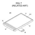
- FIGS. 6 and 7 show a conventional OLED display 200, which is used as a comparative example.
- the OLED display 200 includes a bezel 510 having a bottom portion 54 on which a panel assembly 20 is disposed, and sidewalls 56 extending from side edges of the bottom portion 54, except for a side edge at which an FPCB 32 is bent toward the panel assembly 20.
- a double-sided adhesive tape 58 is located between the bottom portion 54 of the bezel 510 and the panel assembly 20, to fix the panel assembly 20 on the bezel 510.
- the thickness of the panel assembly 20 is 0.41 mm
- the thickness of the bottom portion 54 of the bezel 510 is 0.15
- the thickness of the double-sided adhesive tape 58 is 0.03
- the thickness of a polarizing plate (not shown), attached on an outer surface of the second substrate 14, is 0.15mm. Therefore, an overall thickness of the comparative OLED display 200 is 0.74mm.
- Example 1 5 test samples of Example 1, each of which was made by associating the bezel 410 without the impact absorption member 52, with the panel assembly 20 having the display region A10, whose diagonal length is 55.88mm (2.2 inches), were prepared.
- 10 test samples of Example 2 each of which is made by varying a width of the bezel of the OLED display of Example 1, were also prepared.
- the thickness of the panel assembly 20 With regard to Examples 1, 2, and 3, the thickness of the panel assembly 20, the thickness of the polarizing plate disposed on the outer surface of the second substrate 14, the thickness of the impact absorption member 52, and the width W and thickness T of the bezel 410, are shown in the following table 1.
- Table 1 Thickness of Panel Assembly (mm) Thickness of Polarizing plate Thickness of Impact Absorption Member (mm) Thickness of Bezel (mm) Width of Bezel (mm)
- Example 1 0.41 0.15 0 0.74 1.05
- Example 2 0.41 0.15 0 0.74 2
- Example 3 0.41 0.15 0.15 0.74 1.7
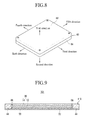
- a drop test for determining damage to the panel assembly 20, was performed by allowing a drop jig, with each of the test samples attached thereto, to execute a free-fall from a height of 1.8m.
- the drop jig 60 includes an upper case 62 and a lower case 64.
- An OLED display is mounted in a space defined by the upper and lower cases 62 and 64.
- the drop jig 60 was dropped in the first through sixth directions, as indicated by the arrows. The drop test was performed 18 times (3 times for each of the six directions) for each test sample.
- Drop impact resistance points of each test sample, total drop impact resistance points, and average of the drop impact resistance points, of the Comparative Example and Examples 1 to 3, are shown in the following table 2.
- the drop impact resistance points were calculated, by giving 1 point when the panel assembly 20 is not damaged, and by giving 0 points when the panel assembly 20 is damaged.
- Example 3 Test Samples 1 6 6 13 18 2 1 0 18 18 3 1 12 18 18 4 1 13 18 18 5 7 18 18 18 6 13 - 1 18 7 13 - 6 18 8 7 - 16 18 9 1 - 1 - 10 1 - 18 - 11 12 - - - 12 1 - - - Total 64 49 127 160 Average 5.3 9.8 12.7 16
- the OLED displays of Examples 1 to 3 have more drop impact resistance points than the OLED displays 200 of the Comparative Example. That is, in the OLED displays 200 of the Comparative Example, the bottom portion 54 of the bezel 510 was easily deformed by the external impacts, and the deformation of the bottom portion 54 directly affected the panel assembly 20. As a result, the panel assembly 20 was easily damaged. On the other hand, in the OLED displays 100 of Examples 1 to 3, since the bottom portion was omitted from the bezel, and the strength of the bezel was enhanced, the damage of the panel assembly was suppressed, as shown in Table 2.
- the OLED display of Example 3 having the impact absorption member 52, had more drop impact resistance points than the OLED displays of Examples 1 and 2. That is, the OLED display of Example 3 had a higher mechanical strength than the OLED displays of Examples 1 and 2.
- FIG. 9 is a cross-sectional view of an OLED display 101, according to a second exemplary embodiment of the present disclosure.
- the OLED display 101 is similar to the OLED display 100, except that a filler 66 is located between a panel assembly 20 and a bezel 410.
- like reference numbers are used to refer to like parts.
- the filler 66 is formed of a material having high impact-resistance and flexibility.
- the filler 66 may be formed of an epoxy resin.
- the filler 66 increases the fixing force applied to the panel assembly 20, and attenuates impacts transferred from the bezel 410 to the panel assembly 20, thereby protecting the panel assembly 20.
- FIG. 10 is an OLED display 102, according to a third exemplary embodiment of the present disclosure
- FIG. 11 is a perspective view of a bezel 420 depicted in FIG. 10
- the OLED display 102 includes a panel assembly 20, the bezel 420, and a fixing member 503 disposed between the panel assembly 20 and the bezel 420.
- the fixing member 503 may be formed of an epoxy resin having a high viscosity, a high flexibility, and a high impact-resistance.
- One short side portion of the bezel 420 which corresponds to a pad region A20, is omitted. That is, the bezel 420 includes a pair of long side portions 44' and one short side portion 46'.
- the bezel 420 is formed to have a high flexibility.
- the bezel 420 may be formed of a synthetic resin, rather than a metal.
- the bezel 420 has a plurality of grooves 68 on top and bottom surfaces thereof, to reduce the thickness/weight of the bezel 420 at various locations.
- the OLED display 102 is similar to the OLED display 100, except a fixing member 503 and a bezel 420 are modified. Like reference numbers are used to refer to like parts.
- panel assemblies are manufactured by simultaneously forming a plurality of panel assemblies on a mother substrate, and cutting the mother substrate in units corresponding to the panel assemblies. At this point, fine cracks may be formed on side surfaces of the panel assembly 20, as a cutting wheel passes through the mother substrate. External impacts are generally transferred to the panel assembly 20, through the side surfaces of the panel assembly 20. Therefore, damage to the panel assembly 20 begins at the side surfaces.
- the bezel 420 is located around the outer perimeter of the panel assembly 20, the mechanical strength of the side surfaces (the outer perimeter) of the panel assembly 20 is enhanced, and the resistance to bending force is increased, thereby effectively protecting the panel assembly 20 from external impacts.
- the panel assembly 20 can be protected from damage that can occur during mounting of the OLED display 102 on an electronic device, or when conveying the OLED display 102.
- the quality of products incorporating the OLED display 102 can be improved.
- FIG. 12 is a perspective view of a modified example of a bezel 430 of the third exemplary embodiment.
- the bezel 430 is similar to the bezel 420 of the third exemplary embodiment, except that a plurality of grooves 70 are formed on inner and outer side surfaces of a bezel 430, to partly reduce a width/weight of the bezel 430.
- FIG. 13 is a perspective view of another modified example of a bezel 440 of the third exemplary embodiment.
- the bezel 440 is similar to the bezel 420 of the third exemplary embodiment, except that a plurality of holes 72 are formed on inner and outer side surfaces of a bezel 440.
- FIG. 14 is a perspective view of another modified example of a bezel 450 of the third exemplary embodiment.
- the bezel 450 is similar to the bezel 420 of the third exemplary embodiment, except that a plurality of holes 74 are formed in front and rear surfaces of a bezel 450.
Landscapes
- Physics & Mathematics (AREA)
- Optics & Photonics (AREA)
- Electroluminescent Light Sources (AREA)
- Devices For Indicating Variable Information By Combining Individual Elements (AREA)
Abstract
Description
- Aspects of the present disclosure relate to an organic light emitting diode (OLED) display. More particularly, aspects of the present disclosure relate to an OLED display having enhanced mechanical strength, due to an improved bezel that supports a panel assembly.
- An OLED display includes a plurality of OLEDs, each having a hole injection electrode, an organic emissive layer, and an electron injection electrode. The OLEDs emit light using energy generated when excitons, generated by electron-hole combinations in the organic light emitting layer, drop from an excitation state to a ground state.
- By the above principle, OLED displays have a self-emissive characteristic. Therefore, unlike liquid crystal displays (LCDs), OLED displays do not require a separate light source, and thus, the thickness and weight thereof can be reduced. Further, OLED displays have low power consumption, high luminance, quick response, and the like. Therefore, OLED displays are drawing attention as the preferred displays for portable electronic devices.
- Generally, a typical OLED display includes a panel assembly in which OLEDs are formed, a bezel coupled to the panel assembly, at a rear side of the panel assembly, and a printed circuit board (PCB) electrically connected to the panel assembly, by a flexible printed circuit board (FPCB). A panel assembly of an LCD includes two thin substrates, and liquid crystal filled in a space between these substrates. Unlike an LCD, an OLED display is designed such that empty spaces exist inside of the panel assembly. Therefore, the mechanical strength of an OLED may be compromised.
- Therefore, when a user accidentally drops an electronic device having an OLED display, relatively large torsion loads and/or relatively large bending loads are applied to the bezel, and thus, the bezel is deformed. As a result, the torsion loads and/or the bending loads are transferred to the panel assembly, which is coupled to the bezel. This may cause damage to the panel assembly.
- The above information is disclosed for enhancement of understanding of the background of the invention, and therefore, it may contain information that does not constitute prior art.
- Exemplary embodiments of the present disclosure provide an OLED display having enhanced mechanical strength and impact resistance, due to an improved bezel, which is coupled to a panel assembly.
- In an exemplary embodiment of the present disclosure, an organic light emitting diode (OLED) display includes: a panel assembly comprising a display region, a pad region, and a plurality of OLEDs formed in the display region; a bezel disposed around the panel assembly; and a fixing member to fix the panel assembly to the bezel.
- Preferably, the bezel may be provided such that it frames edges of the panel assembly only and not a bottom surface of the panel assembly.
- In an exemplary embodiment of the present disclosure, the fixing member may be located on a rear surface of the panel assembly and a rear surface of the bezel. The fixing member may include a base layer, and an adhesive layer formed on a surface of the base layer, which faces the panel assembly and the bezel.
- In an exemplary embodiment of the present disclosure, the bezel may have a frame structure and may include a pair of long side portions, between which an opening is defined, and a pair of short side portions, between which the opening is also defined. One of the short side portions, which corresponds to the pad region, is provided with a recess portion. The OLED display may further include: a flexible printed circuit board fixed on the pad region, and bent toward a rear surface of the fixing member, and enclosing the recess portion; and a printed circuit board electrically connected to the flexible printed circuit board.
- In an exemplary embodiment of the present disclosure, the OLED display may include an impact absorption member located between the panel assembly and the fixing member. The impact absorption member may include an impact absorption layer formed of a sponge material or of urethane, and an adhesive layer formed on a surface of the impact absorption layer, facing the panel assembly.
- In an exemplary embodiment of the present disclosure, a top surface of the bezel may be located horizontally, at a level equal to, or higher than, a top surface of the panel assembly. The width of the bezel may be greater than the thickness of the bezel. Preferably, the width may be 40% larger than the thickness of the bezel, more preferably twice as large as the thickness. The bezel may be spaced apart from an outer perimeter of the panel assembly.
- In an exemplary embodiment of the present disclosure, the OLED display may include a filler located between the panel assembly and the bezel. The bezel may be formed of one of stainless steel, cold drawn steel, aluminum, an aluminum alloy, a magnesium alloy, and a nickel alloy.
- In an exemplary embodiment of the present disclosure, the fixing member may be located between the panel assembly and the bezel. The bezel may correspond to side surfaces of the panel assembly, except for a side surface corresponding to the pad region. The bezel may be formed of a synthetic resin.
- In an exemplary embodiment of the present disclosure, a plurality of grooves or holes may be formed in at least one surface of the bezel. Preferably, the grooves may be formed on a front surface and a rear surface of the bezel, to partly reduce a thickness/weight of the bezel. Alternatively, a plurality of grooves may be formed on inner and outer side surfaces of the bezel, to partly reduce a width/weight of the bezel. Alternatively, a plurality of holes may be formed in the front surface and the rear surface of the bezel. Alternatively, a plurality of holes may be formed in inner and outer side surfaces of the bezel.
- In a further embodiment of the present invention an organic light emitting diode display may be provided, comprising a panel assembly which comprises a display region, a pad region, and a plurality of OLEDs formed in the display region. The OLED display may further comprise a bezel having an opening into which the panel assembly is disposed; and a fixing member disposed on a rear surface of the bezel, to fix the panel assembly to the bezel.
- Preferably, the edges of the panel assembly are spaced apart from the bezel.
- The display may further comprise a filler disposed between the panel assembly and the bezel.
- The bezel may extend around three sides of the panel assembly.
- Grooves may be formed in at least one surface of the bezel.
- An impact absorption member may be disposed between the panel assembly and the fixing member.
- Additional aspects and/or advantages of the invention will be set forth in part in the description which follows and, in part, will be obvious from the description, or may be learned by practice of the invention.
- These and/or other aspects and advantages of the invention will become apparent, and more readily appreciated, from the following description of the exemplary embodiments, taken in conjunction with the accompanying drawings, of which:
-
FIG. 1 is an exploded perspective view of an OLED display, according to a first exemplary embodiment of the present disclosure; -
FIG. 2 is an assembled perspective view of the OLED display ofFIG. 1 ; -
FIG. 3 is a cross-sectional view taken along line I-I ofFIG. 2 ; -
FIG. 4 is a circuit diagram of a sub-pixel circuit of a panel assembly depicted inFIG. 1 ; -
FIG. 5 is an enlarged cross-sectional view of a portion of the panel assembly depicted inFIG. 1 ; -
FIG. 6 is an exploded perspective of an OLED display of a comparative example; -
FIG. 7 is an assembled perspective view of the OLED display ofFIG. 6 ; -
FIG. 8 is a schematic diagram of a drop jig used for a drop test; -
FIG. 9 is a cross-sectional view of an OLED display, according to a second exemplary embodiment of the present disclosure; -
FIG. 10 is an OLED display, according to a third exemplary embodiment of the present disclosure; -
FIG. 11 is a perspective view of a bezel of the OLED display ofFIG. 10 ; -
FIG. 12 is a perspective view of a modified example of the bezel ofFIG. 11 ; -
FIG. 13 is a perspective view of another modified example of the bezel ofFIG. 11 ; and -
FIG. 14 is a perspective view of still another modified example of the bezel ofFIG. 11 . - Reference will now be made in detail to the exemplary embodiments of the present invention, examples of which are illustrated in the accompanying drawings, wherein like reference numerals refer to the like elements throughout. The exemplary embodiments are described, below in order to explain the aspects of the present invention, by referring to the figures.
-
FIG. 1 is an exploded perspective view of anOLED display 100, according to a first exemplary embodiment of the present disclosure,FIG. 2 is an assembled perspective view of theOLED display 100, andFIG. 3 is a cross-sectional view taken along line I-I, ofFIG. 2 . Referring toFIGS. 1 to 3 , theOLED display 100 includes: apanel assembly 20 having a display region A10 to display an image, and a pad region A20; abezel 410 coupled to thepanel assembly 20; and a printed circuit board (PCB) 36 electrically connected to thepanel assembly 20, via a flexible printed circuit board (FPCB) 32. - The
panel assembly 20 includes afirst substrate 12 and asecond substrate 14. Thesecond substrate 14 is smaller than thefirst substrate 12, and has a peripheral portion coupled to thefirst substrate 12, by a sealant. The display region A10 is defined at an overlapping region of the first andsecond substrates - A plurality of sub-pixels are disposed in a matrix pattern, in the display region A10 of the
first substrate 12. Scan and data drivers (not shown) to drive the sub-pixels, are located between the display region A10 and the sealant, or outside of the sealant. Pad electrodes (not shown) transfer electric signals to the scan and data drivers, and are located in the pad region A20. -
FIG. 4 is a circuit diagram of a sub-pixel circuit of thepanel assembly 20, andFIG. 5 is an enlarged cross-sectional view of a portion of thepanel assembly 20. Referring toFIGS. 4 and FIG. 5 , each of the sub-pixels of thepanel assembly 20 includes an OLED L1 and a driving circuit unit. The OLED L1 includes ananode electrode 16, an organicemissive layer 18, and acathode electrode 22. The driving circuit unit includes at least two thin film transistors and at least one storage capacitor C1. The thin film transistors include at least one switching transistor T1 and at least one driving transistor T2. - The switching transistor T1 is connected to scan and data lines SL1 and DL1, to transfer a data voltage, which is an input from the data line DL1, in accordance with a switching voltage input to the scan line SL1, to the driving transistor T2. The storage capacitor C1 is connected to a power line VDD, as well as to the switching transistor T1, to store a voltage corresponding to a difference between a voltage transferred from the switching transistor T1, and a voltage supplied from the power line VDD.
- The driving transistor T2 is connected to both the power line VDD and the storage capacity C1, to supply an output current IOLED to the OLED L1, which corresponds to a square of the difference between a voltage stored in the storage capacity C1, and a threshold voltage. The OLED L1 can emit light using the output current IOLED. The driving transistor T2 includes a
source electrode 24, adrain electrode 26, and agate electrode 28. Theanode electrode 16 is connected to thedrain electrode 26. The above-described structure of the sub-pixels is exemplary only, and may be modified in various ways. - The
second substrate 14 is coupled to thefirst substrate 12 by the sealant, at a predetermined interval, to protect the driving circuit unit and the OLEDs on thefirst substrate 12 from an external environment. A polarizing plate (not shown) to suppress reflections of external light, may be located on an outer surface of thesecond substrate 14, at the display region A10. A moisture absorption agent (not shown) may be attached on an inner surface of thesecond substrate 14. - Referring again to
FIGS. 1 to 3 , anintegrated circuit chip 30 is mounted at the pad region A20 of thepanel assembly 20, through a chip-on-glass (COG) method. TheFPCB 32 is also mounted at the pad region A20, through a chip-on-film (COF) method. Aprotective layer 34 is formed around theintegrated circuit chip 30 and theFPCB 32, to cover and protect pad electrodes formed at the pad region A20. - A variety of electronic elements (not shown) for processing driving signals are mounted on the
PCB 36. Aconnector 38, to transfer external signals to thePCB 36, is also installed on the printedcircuit board 36. In the present exemplary embodiment, thebezel 410 has a frame structure framing the edges of the panel assembly and not the bottom surface of the panel assembly. Thebezel 410 includes a pair oflong side portions 44, between which anopening 42 is defined, and a pair ofshort side portions 46, between which theopening 42 is also defined. Thepanel assembly 20 is fitted in theopening 42, such that thebezel 410 is located around the perimeter of thepanel assembly 20. That is, thebezel 410 is not provided with a bottom portion, on which thepanel assembly 20 is disposed. Therefore, the perimeter of thepanel assembly 20 is facing the inner surface of thebezel 410. - A fixing
member 50, to fix thebezel 410 and thepanel assembly 20, is disposed on rear surfaces of thepanel assembly 20 andbezel 410. The fixingmember 50 may be a single-sided adhesive tape, having abase layer 501 and anadhesive layer 502 formed on a surface of thebase layer 501, which faces thepanel assembly 20 and the bezel 410 (seeFIG. 1 ). Therefore, thepanel assembly 20 is fixed to a central portion of the fixingmember 50, and thebezel 410 is fixed on a peripheral portion of the fixingmember 50. As a result, thepanel assembly 20 and thebezel 410 are coupled to each other, by the fixingmember 50, while at the same time thebezel 410 and panel assembly are provided spaced apart. - The
FPCB 32, which is fixed at the pad region A20, is folded toward a rear surface of the fixingmember 50, at one of theshort side portions 46 of thebezel 410. One of theshort side portions 46 is provided with arecess portion 48, through which theFPCB 32 passes. Thus, the respectiveshort portion 46 has a stepped profile with thicker or higher portions where theFPCB 32 does not pass relative to portions where theFPCB 32 is arranged. That is, a front surface of therecess portion 48 is lower than a front surface of theshort side portions 46. Therefore, theFPCB 32 is bent toward the rear surface of the fixingmember 50, while enclosing theshort side portion 46 that includes therecess portion 48. - An
impact absorption member 52 may be located between thepanel assembly 20 and the fixingmember 50, to absorb external impacts. Theimpact absorption member 52 includes animpact absorption layer 521 and anadhesive layer 522 formed on a surface of theimpact absorption layer 521, which faces the panel assembly 20 (seeFIG. 3 ). Theimpact absorption layer 521 may be flexible and may be formed of a sponge material or urethane. Theimpact absorption member 52 attenuates external impacts applied to thepanel assembly 20, to protect thepanel assembly 20. - The front surface of the
bezel 410 may be located in the same plane as the front surface of thepanel assembly 20, or may be located in front of the front surface of thepanel assembly 20. As referred to herein, the front surface of theOLED display 100, and the various components thereof, relates to the surface upon which an image is displayed. That is, if theimpact absorption member 52 is not provided, a thickness of thebezel 410 may be equal to, or greater than, that of thepanel assembly 20. When theimpact absorption member 52 is provided, the thickness of thebezel 410 may be equal to, or greater than, the sum of the thicknesses of thepanel assembly 20 and theimpact absorption member 52. -
FIG. 3 shows an exemplary embodiment where a thickness T of thebezel 410 is the same as the sum of the thicknesses of thepanel assembly 20 and theimpact absorption member 52. If the front surface of thebezel 410 is lower than the front surface of thepanel assembly 20, an impact load, which is generated when an external impact is applied to theOLED display 100, is directly transferred to thepanel assembly 20. This may damage thepanel assembly 20. - The outer perimeter (side surfaces) of the
panel assembly 20 may be spaced apart from the inner wall (inner perimeter) of thebezel 410, by a gap G (seeFIG. 3 ). Therefore, even when thebezel 410 is deformed by an external impact, the deformation of thebezel 410 does not directly affect thepanel assembly 20. In order to enable theimpact absorption member 52 to contact thebezel 410, theimpact absorption member 52 may be formed to have a larger surface area than the panel assembly 20 (seeFIG. 3 ). - In order to have a proper strength, the
bezel 410 is designed to have a width W that is greater than the thickness (or height) T (seeFIG. 3 ). The width W may be at least 40% greater than the thickness T or may be at least twice as large as the thickness T. If the width W of thebezel 410 is less than the thickness T, thebezel 410 may not have a sufficient resistance to bending. - When it is assumed that an overall thickness of the
panel assembly 20, including a polarizing plate (not shown), is 0.56mm, and theimpact absorption member 52 is omitted, thebezel 410 is designed to have a width W of about 1.05mm, and a thickness T of about 0.74mm. However, the width W and thickness T of thebezel 410 are not so limited, and may vary in accordance with the size and thickness of thepanel assembly 20. - The
bezel 410 may be formed of a high strength metal, such as stainless steel, cold drawn steel, aluminum, an aluminum alloy, a magnesium alloy, a nickel alloy, and the like. The aluminum alloy and the magnesium alloy are lightweight materials, and they can be used to reduce an overall weight of theOLED display 100. - As the
bezel 410 is formed in a frame shape, and has a thickness greater than thepanel assembly 20, the strength of thebezel 410 can be enhanced, and thus, the deformations of thebezel 410 can be reduced. Further, since the inner perimeter of thebezel 410 is spaced apart from the outer perimeter of thepanel assembly 20, by the gap G, the deformation of thebezel 410 does not directly affect thepanel assembly 20, and thus, thepanel assembly 20 can be further protected. - 12 Comparative Examples, each including a conventional bezel, and an associated a panel assembly having a display region whose a diagonal length is 55.88mm (2.2 inches), were prepared.
FIGS. 6 and7 show aconventional OLED display 200, which is used as a comparative example. TheOLED display 200 includes abezel 510 having abottom portion 54 on which apanel assembly 20 is disposed, and sidewalls 56 extending from side edges of thebottom portion 54, except for a side edge at which anFPCB 32 is bent toward thepanel assembly 20. A double-sidedadhesive tape 58 is located between thebottom portion 54 of thebezel 510 and thepanel assembly 20, to fix thepanel assembly 20 on thebezel 510. - In
FIGS. 1 ,6 , and7 , like reference numbers refer to like parts, except for the bezels. In thecomparative OLED display 200, the thickness of thepanel assembly 20 is 0.41 mm, the thickness of thebottom portion 54 of thebezel 510 is 0.15, the thickness of the double-sidedadhesive tape 58 is 0.03, and the thickness of a polarizing plate (not shown), attached on an outer surface of thesecond substrate 14, is 0.15mm. Therefore, an overall thickness of thecomparative OLED display 200 is 0.74mm. - Referring again to
FIGS. 1-3 ,5 test samples of Example 1, each of which was made by associating thebezel 410 without theimpact absorption member 52, with thepanel assembly 20 having the display region A10, whose diagonal length is 55.88mm (2.2 inches), were prepared. In addition, 10 test samples of Example 2, each of which is made by varying a width of the bezel of the OLED display of Example 1, were also prepared. Further, 10 test samples of Example 3, each of which was made by associating thebezel 410 having theimpact absorption member 52, with thepanel assembly 20 having the display region A10, whose diagonal length is 55.88mm (2.2 inches), were also prepared. - With regard to Examples 1, 2, and 3, the thickness of the
panel assembly 20, the thickness of the polarizing plate disposed on the outer surface of thesecond substrate 14, the thickness of theimpact absorption member 52, and the width W and thickness T of thebezel 410, are shown in the following table 1.[Table 1] Thickness of Panel Assembly (mm) Thickness of Polarizing plate Thickness of Impact Absorption Member (mm) Thickness of Bezel (mm) Width of Bezel (mm) Example 1 0.41 0.15 0 0.74 1.05 Example 2 0.41 0.15 0 0.74 2 Example 3 0.41 0.15 0.15 0.74 1.7 - A drop test, for determining damage to the
panel assembly 20, was performed by allowing a drop jig, with each of the test samples attached thereto, to execute a free-fall from a height of 1.8m. -
FIG. 8 is a schematic diagram of adrop jig 60 used for the drop test. - The
drop jig 60 includes anupper case 62 and alower case 64. An OLED display is mounted in a space defined by the upper andlower cases drop jig 60 was dropped in the first through sixth directions, as indicated by the arrows. The drop test was performed 18 times (3 times for each of the six directions) for each test sample. - Drop impact resistance points of each test sample, total drop impact resistance points, and average of the drop impact resistance points, of the Comparative Example and Examples 1 to 3, are shown in the following table 2. In the 18 drop tests, the drop impact resistance points were calculated, by giving 1 point when the
panel assembly 20 is not damaged, and by giving 0 points when thepanel assembly 20 is damaged.[Table 2] Drop Impact Resistance Point Comparative Example Example 1 Example 2 Example 3 Test Samples 1 6 6 13 18 2 1 0 18 18 3 1 12 18 18 4 1 13 18 18 5 7 18 18 18 6 13 - 1 18 7 13 - 6 18 8 7 - 16 18 9 1 - 1 - 10 1 - 18 - 11 12 - - - 12 1 - - - Total 64 49 127 160 Average 5.3 9.8 12.7 16 - As shown in Table 1, the OLED displays of Examples 1 to 3 have more drop impact resistance points than the OLED displays 200 of the Comparative Example. That is, in the OLED displays 200 of the Comparative Example, the
bottom portion 54 of thebezel 510 was easily deformed by the external impacts, and the deformation of thebottom portion 54 directly affected thepanel assembly 20. As a result, thepanel assembly 20 was easily damaged. On the other hand, in the OLED displays 100 of Examples 1 to 3, since the bottom portion was omitted from the bezel, and the strength of the bezel was enhanced, the damage of the panel assembly was suppressed, as shown in Table 2. - Particularly, it can be noted that the OLED display of Example 3, having the
impact absorption member 52, had more drop impact resistance points than the OLED displays of Examples 1 and 2. That is, the OLED display of Example 3 had a higher mechanical strength than the OLED displays of Examples 1 and 2. -
FIG. 9 is a cross-sectional view of anOLED display 101, according to a second exemplary embodiment of the present disclosure. Referring toFIG. 9 , theOLED display 101 is similar to theOLED display 100, except that afiller 66 is located between apanel assembly 20 and abezel 410. In the first and second exemplary embodiments, like reference numbers are used to refer to like parts. - The
filler 66 is formed of a material having high impact-resistance and flexibility. For example, thefiller 66 may be formed of an epoxy resin. Thefiller 66 increases the fixing force applied to thepanel assembly 20, and attenuates impacts transferred from thebezel 410 to thepanel assembly 20, thereby protecting thepanel assembly 20. -
FIG. 10 is anOLED display 102, according to a third exemplary embodiment of the present disclosure, andFIG. 11 is a perspective view of abezel 420 depicted inFIG. 10 . Referring toFIGS. 10 and11 , theOLED display 102 includes apanel assembly 20, thebezel 420, and a fixingmember 503 disposed between thepanel assembly 20 and thebezel 420. The fixingmember 503 may be formed of an epoxy resin having a high viscosity, a high flexibility, and a high impact-resistance. One short side portion of thebezel 420, which corresponds to a pad region A20, is omitted. That is, thebezel 420 includes a pair of long side portions 44' and one short side portion 46'. - The
bezel 420 is formed to have a high flexibility. For example, thebezel 420 may be formed of a synthetic resin, rather than a metal. Thebezel 420 has a plurality ofgrooves 68 on top and bottom surfaces thereof, to reduce the thickness/weight of thebezel 420 at various locations. - The
OLED display 102 is similar to theOLED display 100, except a fixingmember 503 and abezel 420 are modified. Like reference numbers are used to refer to like parts. - Generally, panel assemblies are manufactured by simultaneously forming a plurality of panel assemblies on a mother substrate, and cutting the mother substrate in units corresponding to the panel assemblies. At this point, fine cracks may be formed on side surfaces of the
panel assembly 20, as a cutting wheel passes through the mother substrate. External impacts are generally transferred to thepanel assembly 20, through the side surfaces of thepanel assembly 20. Therefore, damage to thepanel assembly 20 begins at the side surfaces. - In the
OLED display 102, thebezel 420 is located around the outer perimeter of thepanel assembly 20, the mechanical strength of the side surfaces (the outer perimeter) of thepanel assembly 20 is enhanced, and the resistance to bending force is increased, thereby effectively protecting thepanel assembly 20 from external impacts. Thepanel assembly 20 can be protected from damage that can occur during mounting of theOLED display 102 on an electronic device, or when conveying theOLED display 102. Thus, the quality of products incorporating theOLED display 102 can be improved. -
FIG. 12 is a perspective view of a modified example of abezel 430 of the third exemplary embodiment. Thebezel 430 is similar to thebezel 420 of the third exemplary embodiment, except that a plurality ofgrooves 70 are formed on inner and outer side surfaces of abezel 430, to partly reduce a width/weight of thebezel 430. -
FIG. 13 is a perspective view of another modified example of abezel 440 of the third exemplary embodiment. Thebezel 440 is similar to thebezel 420 of the third exemplary embodiment, except that a plurality ofholes 72 are formed on inner and outer side surfaces of abezel 440. -
FIG. 14 is a perspective view of another modified example of abezel 450 of the third exemplary embodiment. Thebezel 450 is similar to thebezel 420 of the third exemplary embodiment, except that a plurality ofholes 74 are formed in front and rear surfaces of abezel 450.
Claims (18)
- An organic light emitting diode (OLED) (100) display comprising:a panel assembly (20) comprising a display region (A10), a pad region (A20), and a plurality of OLEDs formed in the display region (A10);a bezel (410) disposed around the panel assembly (20); anda fixing member (50) to fix the panel assembly (20) to the bezel (410),characterized in thatthe panel assembly (20) is provided spaced apart from the bezel (410).
- The OLED display (100) of claim 1, wherein the bezel (410) is provided such that it frames edges of the panel assembly (20) and not a bottom surface of the panel assembly (20).
- The OLED display (100) of claim 1 or 2, wherein the fixing member (50) is disposed on a rear surface of the panel assembly (20), and on a rear surface of the bezel (410).
- The OLED display (100) of any of the previous claims, wherein the fixing member (50) comprises a base layer (501) and an adhesive layer (502) formed on a surface of the base layer (501), the adhesive layer (502) facing the panel assembly (20) and the bezel (410).
- The OLED display (100) of any of the previous claims, wherein the bezel (410) has a frame structure and/or consists of a pair of long side portions (44), and a pair of short side portions (46), and the long and short side portions (44, 46) defining an opening (42), and one of the short side portions (46), which corresponds to the pad region (A20), has a recess portion (48).
- The OLED display (100) of claim 5, further comprising:a flexible printed circuit board (32) fixed on the pad region (A20), andbent toward a rear surface of the fixing member (50), around the recess portion (48); anda printed circuit board (36) electrically connected to the flexible printed circuit board (32).
- The OLED display (100) of any of the previous claims, further comprising an impact absorption member (52) disposed between the panel assembly (20) and the fixing member (50).
- The OLED display (100) of claim 7, wherein the impact absorption member (52) comprises an impact absorption layer (521) and an adhesive layer (522) formed on a surface of the impact absorption layer (521), which faces the panel assembly (20),
wherein the impact absorption layer (521) is formed of a sponge material or a urethane material. - The OLED display (100) of any of the previous claims, wherein a front surface of the bezel (410) is in the same plane as, or is disposed in front of, a front surface of the panel assembly (20).
- The OLED display (100) of any of the previous claims, wherein the width (W) of the bezel (410) is greater than the thickness (T) of the bezel (410).
- The OLED display (100) of claim 7, wherein the impact absorption member (52) extends into a space between the bezel (410) and the panel assembly (20).
- The OLED display (100) of any of the previous claims, further comprising a filler (66) located between the panel assembly (20) and the bezel (410).
- The OLED display (100) of any of the previous claims, wherein the bezel (410) is formed of one of stainless steel, cold drawn steel, aluminum, an aluminum alloy, a magnesium alloy, and a nickel alloy.
- The OLED display (100) of any of the previous claims, wherein the bezel (410) is disposed around four edges of the panel assembly (20).
- The OLED display (100) of any of the previous claims 1 to 13,
wherein the bezel (420, 430, 440, 450) is disposed around three edges of the panel assembly (20), and is not disposed around an edge of the panel assembly (20) that is adjacent to the pad region (A20). - The OLED display (100) of claim 15, wherein grooves (68, 70) are formed in at least one surface of the bezel or wherein grooves (68) are formed on a front surface and a rear surface of the bezel (420) orwherein grooves (70) are formed on inner and outer side surfaces of the bezel (430).
- The OLED display (100) of claim 15, wherein holes (72, 74) are formed in at least one surface of the bezel or wherein holes (74) are formed in front and rear surfaces of the bezel (450) orwherein holes (72) are formed in inner and outer side surfaces of the bezel (440).
- The OLED display (100) of claim 15, wherein the bezel (420, 430, 440, 450) is formed of a synthetic resin.
Applications Claiming Priority (1)
| Application Number | Priority Date | Filing Date | Title |
|---|---|---|---|
| KR1020080011138A KR100922357B1 (en) | 2008-02-04 | 2008-02-04 | Organic light emitting display |
Publications (2)
| Publication Number | Publication Date |
|---|---|
| EP2086008A1 true EP2086008A1 (en) | 2009-08-05 |
| EP2086008B1 EP2086008B1 (en) | 2011-06-22 |
Family
ID=40459243
Family Applications (1)
| Application Number | Title | Priority Date | Filing Date |
|---|---|---|---|
| EP09151085A Ceased EP2086008B1 (en) | 2008-02-04 | 2009-01-22 | Organic light emitting diode display |
Country Status (3)
| Country | Link |
|---|---|
| US (1) | US7957128B2 (en) |
| EP (1) | EP2086008B1 (en) |
| KR (1) | KR100922357B1 (en) |
Cited By (2)
| Publication number | Priority date | Publication date | Assignee | Title |
|---|---|---|---|---|
| EP2599618A1 (en) * | 2011-11-30 | 2013-06-05 | Samsung Display Co., Ltd. | Cushion sheet and display device having the same |
| EP2712002A3 (en) * | 2012-09-19 | 2016-11-16 | Samsung Display Co., Ltd. | Organic light emitting diode display |
Families Citing this family (8)
| Publication number | Priority date | Publication date | Assignee | Title |
|---|---|---|---|---|
| US7966861B2 (en) * | 2007-12-27 | 2011-06-28 | Samsung Mobile Display Co., Ltd. | Jig frame for drop test of flat panel display device |
| KR100918053B1 (en) * | 2007-12-27 | 2009-09-22 | 삼성모바일디스플레이주식회사 | Organic light emitting display |
| KR101127592B1 (en) * | 2010-04-06 | 2012-03-23 | 삼성모바일디스플레이주식회사 | Organinc light emitting display device and electronic equipment having the same |
| US8611077B2 (en) * | 2010-08-27 | 2013-12-17 | Apple Inc. | Electronic devices with component mounting structures |
| KR101792095B1 (en) * | 2010-10-22 | 2017-11-02 | 삼성디스플레이 주식회사 | Display divce |
| KR101810998B1 (en) | 2011-06-29 | 2017-12-21 | 삼성디스플레이 주식회사 | Display device |
| KR101542411B1 (en) * | 2013-04-17 | 2015-08-12 | 엘지전자 주식회사 | Mobile terminal |
| CN108963075B (en) * | 2018-07-23 | 2022-03-22 | 广州国显科技有限公司 | Support film, preparation method thereof, display module and display panel |
Citations (5)
| Publication number | Priority date | Publication date | Assignee | Title |
|---|---|---|---|---|
| US6055029A (en) * | 1996-07-23 | 2000-04-25 | Stanley Electric Co., Ltd. | Backlighting system for a liquid crystal display including an integrally molded light guiding plate and frame with a deformation absorbing means |
| US20050184662A1 (en) * | 2004-02-24 | 2005-08-25 | Eastman Kodak Company | OLED display haivng thermally conductive backplate |
| EP1655128A1 (en) * | 2004-10-13 | 2006-05-10 | Nitto Denko Corporation | Impact-absorbing sheet |
| US20080007159A1 (en) * | 2006-06-08 | 2008-01-10 | Samsung Electronics Co., Ltd. | Organic light-emitting diode display device |
| WO2008057143A1 (en) * | 2006-11-08 | 2008-05-15 | Corning Incorporated | Bezel packaging of frit-sealed oled devices |
Family Cites Families (7)
| Publication number | Priority date | Publication date | Assignee | Title |
|---|---|---|---|---|
| JP2002311428A (en) * | 2001-04-11 | 2002-10-23 | Hitachi Ltd | Liquid crystal display |
| KR20050070543A (en) * | 2003-12-30 | 2005-07-07 | 주식회사 팬택앤큐리텔 | Organic emitting light diode display mounting structure and mobile terminal having the same |
| JP4196888B2 (en) * | 2004-06-25 | 2008-12-17 | セイコーエプソン株式会社 | Electro-optical device and electronic apparatus |
| KR20060034044A (en) * | 2004-10-18 | 2006-04-21 | 삼성전자주식회사 | Display device |
| KR20060039658A (en) * | 2004-11-03 | 2006-05-09 | 엘지전자 주식회사 | Organic electroluminescent device kit |
| JP2006154366A (en) * | 2004-11-30 | 2006-06-15 | Sanyo Electric Co Ltd | Display device and mobile telephone |
| KR100729084B1 (en) * | 2006-09-21 | 2007-06-14 | 삼성에스디아이 주식회사 | Organic electroluminescent display |
-
2008
- 2008-02-04 KR KR1020080011138A patent/KR100922357B1/en not_active Expired - Fee Related
-
2009
- 2009-01-12 US US12/352,058 patent/US7957128B2/en not_active Expired - Fee Related
- 2009-01-22 EP EP09151085A patent/EP2086008B1/en not_active Ceased
Patent Citations (5)
| Publication number | Priority date | Publication date | Assignee | Title |
|---|---|---|---|---|
| US6055029A (en) * | 1996-07-23 | 2000-04-25 | Stanley Electric Co., Ltd. | Backlighting system for a liquid crystal display including an integrally molded light guiding plate and frame with a deformation absorbing means |
| US20050184662A1 (en) * | 2004-02-24 | 2005-08-25 | Eastman Kodak Company | OLED display haivng thermally conductive backplate |
| EP1655128A1 (en) * | 2004-10-13 | 2006-05-10 | Nitto Denko Corporation | Impact-absorbing sheet |
| US20080007159A1 (en) * | 2006-06-08 | 2008-01-10 | Samsung Electronics Co., Ltd. | Organic light-emitting diode display device |
| WO2008057143A1 (en) * | 2006-11-08 | 2008-05-15 | Corning Incorporated | Bezel packaging of frit-sealed oled devices |
Cited By (6)
| Publication number | Priority date | Publication date | Assignee | Title |
|---|---|---|---|---|
| EP2599618A1 (en) * | 2011-11-30 | 2013-06-05 | Samsung Display Co., Ltd. | Cushion sheet and display device having the same |
| CN103137022A (en) * | 2011-11-30 | 2013-06-05 | 三星显示有限公司 | Cushion sheet and display device having the same |
| US9274360B2 (en) | 2011-11-30 | 2016-03-01 | Samsung Display Co., Ltd. | Cushion sheet and display device having the same |
| CN103137022B (en) * | 2011-11-30 | 2017-05-17 | 三星显示有限公司 | Cushion sheet and display device having the same |
| US10076890B2 (en) | 2011-11-30 | 2018-09-18 | Samsung Display Co., Ltd. | Cushion sheet and display device having the same |
| EP2712002A3 (en) * | 2012-09-19 | 2016-11-16 | Samsung Display Co., Ltd. | Organic light emitting diode display |
Also Published As
| Publication number | Publication date |
|---|---|
| EP2086008B1 (en) | 2011-06-22 |
| KR100922357B1 (en) | 2009-10-21 |
| KR20090085311A (en) | 2009-08-07 |
| US7957128B2 (en) | 2011-06-07 |
| US20090195973A1 (en) | 2009-08-06 |
Similar Documents
| Publication | Publication Date | Title |
|---|---|---|
| US8436958B2 (en) | Electronic device having organic light emitting diode display device | |
| EP2086008B1 (en) | Organic light emitting diode display | |
| US8692461B2 (en) | Organic light emitting diode display | |
| KR100918053B1 (en) | Organic light emitting display | |
| KR101792095B1 (en) | Display divce | |
| KR100965251B1 (en) | Organic light emitting display | |
| KR100965252B1 (en) | Organic light emitting display | |
| KR100932982B1 (en) | Display device | |
| KR100989129B1 (en) | Display device | |
| KR20090093058A (en) | Organic light emitting display and electronic device having the same | |
| KR100922360B1 (en) | Organic light emitting display | |
| KR100918054B1 (en) | Organic light emitting display | |
| US7999465B2 (en) | Organic light emitting diode (OLED) display device | |
| US8502446B2 (en) | Organic light emitting diode display | |
| KR101009645B1 (en) | Organic light emitting display | |
| KR100918055B1 (en) | Organic light emitting display | |
| KR20100088884A (en) | Organic light emitting diode display | |
| KR100918056B1 (en) | Organic light emitting display device and electronic device having same | |
| KR101568265B1 (en) | Display Device | |
| KR101474222B1 (en) | Organic light emitting display | |
| KR20090088136A (en) | Organic light emitting display |
Legal Events
| Date | Code | Title | Description |
|---|---|---|---|
| PUAI | Public reference made under article 153(3) epc to a published international application that has entered the european phase |
Free format text: ORIGINAL CODE: 0009012 |
|
| 17P | Request for examination filed |
Effective date: 20090122 |
|
| AK | Designated contracting states |
Kind code of ref document: A1 Designated state(s): AT BE BG CH CY CZ DE DK EE ES FI FR GB GR HR HU IE IS IT LI LT LU LV MC MK MT NL NO PL PT RO SE SI SK TR |
|
| AX | Request for extension of the european patent |
Extension state: AL BA RS |
|
| 17Q | First examination report despatched |
Effective date: 20090918 |
|
| AKX | Designation fees paid |
Designated state(s): DE FR GB |
|
| GRAP | Despatch of communication of intention to grant a patent |
Free format text: ORIGINAL CODE: EPIDOSNIGR1 |
|
| RIN1 | Information on inventor provided before grant (corrected) |
Inventor name: LEE, HYUN-HEE Inventor name: KIM, EUN-AH Inventor name: HA, KUEN-DONG Inventor name: HWANG, HYUN-MIN Inventor name: YEE, DONG-SU Inventor name: MOON, CHAN-KYOUNG |
|
| GRAS | Grant fee paid |
Free format text: ORIGINAL CODE: EPIDOSNIGR3 |
|
| GRAA | (expected) grant |
Free format text: ORIGINAL CODE: 0009210 |
|
| AK | Designated contracting states |
Kind code of ref document: B1 Designated state(s): DE FR GB |
|
| REG | Reference to a national code |
Ref country code: GB Ref legal event code: FG4D |
|
| REG | Reference to a national code |
Ref country code: DE Ref legal event code: R096 Ref document number: 602009001574 Country of ref document: DE Effective date: 20110804 |
|
| PLBE | No opposition filed within time limit |
Free format text: ORIGINAL CODE: 0009261 |
|
| STAA | Information on the status of an ep patent application or granted ep patent |
Free format text: STATUS: NO OPPOSITION FILED WITHIN TIME LIMIT |
|
| 26N | No opposition filed |
Effective date: 20120323 |
|
| REG | Reference to a national code |
Ref country code: DE Ref legal event code: R097 Ref document number: 602009001574 Country of ref document: DE Effective date: 20120323 |
|
| REG | Reference to a national code |
Ref country code: DE Ref legal event code: R082 Ref document number: 602009001574 Country of ref document: DE Representative=s name: GULDE HENGELHAUPT ZIEBIG & SCHNEIDER, DE |
|
| REG | Reference to a national code |
Ref country code: DE Ref legal event code: R081 Ref document number: 602009001574 Country of ref document: DE Owner name: SAMSUNG DISPLAY CO., LTD., KR Free format text: FORMER OWNER: SAMSUNG MOBILE DISPLAY CO. LTD., SUWON, KR Effective date: 20121026 Ref country code: DE Ref legal event code: R082 Ref document number: 602009001574 Country of ref document: DE Representative=s name: GULDE HENGELHAUPT ZIEBIG & SCHNEIDER, DE Effective date: 20121026 Ref country code: DE Ref legal event code: R081 Ref document number: 602009001574 Country of ref document: DE Owner name: SAMSUNG DISPLAY CO., LTD., YONGIN-CITY, KR Free format text: FORMER OWNER: SAMSUNG MOBILE DISPLAY CO. LTD., SUWON, GYEONGGI, KR Effective date: 20121026 Ref country code: DE Ref legal event code: R082 Ref document number: 602009001574 Country of ref document: DE Representative=s name: GULDE & PARTNER PATENT- UND RECHTSANWALTSKANZL, DE Effective date: 20121026 |
|
| REG | Reference to a national code |
Ref country code: GB Ref legal event code: 732E Free format text: REGISTERED BETWEEN 20130103 AND 20130109 |
|
| REG | Reference to a national code |
Ref country code: FR Ref legal event code: TP Owner name: SAMSUNG DISPLAY CO., LTD., KR Effective date: 20130130 |
|
| REG | Reference to a national code |
Ref country code: FR Ref legal event code: PLFP Year of fee payment: 8 |
|
| REG | Reference to a national code |
Ref country code: FR Ref legal event code: PLFP Year of fee payment: 9 |
|
| REG | Reference to a national code |
Ref country code: FR Ref legal event code: PLFP Year of fee payment: 10 |
|
| PGFP | Annual fee paid to national office [announced via postgrant information from national office to epo] |
Ref country code: GB Payment date: 20181220 Year of fee payment: 11 Ref country code: FR Payment date: 20181224 Year of fee payment: 11 |
|
| PGFP | Annual fee paid to national office [announced via postgrant information from national office to epo] |
Ref country code: DE Payment date: 20181219 Year of fee payment: 11 |
|
| REG | Reference to a national code |
Ref country code: DE Ref legal event code: R119 Ref document number: 602009001574 Country of ref document: DE |
|
| GBPC | Gb: european patent ceased through non-payment of renewal fee |
Effective date: 20200122 |
|
| PG25 | Lapsed in a contracting state [announced via postgrant information from national office to epo] |
Ref country code: FR Free format text: LAPSE BECAUSE OF NON-PAYMENT OF DUE FEES Effective date: 20200131 Ref country code: DE Free format text: LAPSE BECAUSE OF NON-PAYMENT OF DUE FEES Effective date: 20200801 Ref country code: GB Free format text: LAPSE BECAUSE OF NON-PAYMENT OF DUE FEES Effective date: 20200122 |