EP2083515A2 - Phase locked loop calibration - Google Patents
Phase locked loop calibration Download PDFInfo
- Publication number
- EP2083515A2 EP2083515A2 EP09000654A EP09000654A EP2083515A2 EP 2083515 A2 EP2083515 A2 EP 2083515A2 EP 09000654 A EP09000654 A EP 09000654A EP 09000654 A EP09000654 A EP 09000654A EP 2083515 A2 EP2083515 A2 EP 2083515A2
- Authority
- EP
- European Patent Office
- Prior art keywords
- signal
- phase
- scaling
- modulation signal
- sign
- Prior art date
- Legal status (The legal status is an assumption and is not a legal conclusion. Google has not performed a legal analysis and makes no representation as to the accuracy of the status listed.)
- Granted
Links
Images

Classifications
-
- H—ELECTRICITY
- H03—ELECTRONIC CIRCUITRY
- H03C—MODULATION
- H03C3/00—Angle modulation
- H03C3/02—Details
- H03C3/09—Modifications of modulator for regulating the mean frequency
- H03C3/0908—Modifications of modulator for regulating the mean frequency using a phase locked loop
- H03C3/0916—Modifications of modulator for regulating the mean frequency using a phase locked loop with frequency divider or counter in the loop
- H03C3/0925—Modifications of modulator for regulating the mean frequency using a phase locked loop with frequency divider or counter in the loop applying frequency modulation at the divider in the feedback loop
-
- H—ELECTRICITY
- H03—ELECTRONIC CIRCUITRY
- H03C—MODULATION
- H03C3/00—Angle modulation
- H03C3/02—Details
- H03C3/09—Modifications of modulator for regulating the mean frequency
- H03C3/0908—Modifications of modulator for regulating the mean frequency using a phase locked loop
- H03C3/0941—Modifications of modulator for regulating the mean frequency using a phase locked loop applying frequency modulation at more than one point in the loop
-
- H—ELECTRICITY
- H03—ELECTRONIC CIRCUITRY
- H03C—MODULATION
- H03C3/00—Angle modulation
- H03C3/02—Details
- H03C3/09—Modifications of modulator for regulating the mean frequency
- H03C3/0908—Modifications of modulator for regulating the mean frequency using a phase locked loop
- H03C3/095—Modifications of modulator for regulating the mean frequency using a phase locked loop applying frequency modulation to the loop in front of the voltage controlled oscillator
Definitions
- the invention relates to an apparatus and method for controlling a modulation signal for modulating a phase locked loop.
- Phase locked loops have a variety of applications, for example in frequency generation in wireless communication equipment.
- a basic phase locked loop comprises a variable frequency oscillator whose frequency and phase is controlled by an error signal, the error signal being generated by a phase detector that compares the phase of the oscillator output signal with the phase of a reference signal.
- the loop contains a low pass filter for filtering the error signal before it is applied to control the oscillator.
- the oscillator operates at a higher frequency than the reference signal, and the loop includes a divider for dividing the oscillator output signal, such that the phase detector compares the divided signal with the reference signal.
- the loop performance depends, among other things, on the gain of the oscillator, the gain being a measure of the change of oscillator frequency in response to a change in the error signal.
- the oscillator is typically an analogue circuit
- the loop performance is susceptible to variations in analogue circuit characteristics, due to, for example, temperature or voltage changes or manufacturing process spread, which lead to variations in oscillator gain.
- a modulation signal can be applied to the input of the oscillator and/or used to control the division ratio of the divider.
- Schemes in which the modulation signal is applied to both the oscillator and the divider are known as two-point modulation schemes.
- variations in oscillator gain will lead to variations in the modulated carrier signal.
- the transfer function for the modulation from the input of the oscillator to the output of the phase locked loop, that is the output of the oscillator is an all-pass filter.
- the oscillator gain is too high, high frequencies of the modulation signal are amplified too much, and if the oscillator gain is too low, high frequencies of the modulation signal are amplified too little.
- WO 2004/034564 discloses a scheme for calibrating oscillator gain in which a correction signal is derived from a phase error signal, and in which the polarity of the error signal is measured by correlating the error signal with a modulation signal.
- US 2007/0103240 discloses a scheme for gain calibration of a digitally controlled oscillator in which a phase error signal is sampled, either continuously or when zero crossings occur in an input data frequency control word, a gradient is generated from the samples and by using the sign of the data, and the oscillator gain estimate is adjusted in accordance with the gradient.
- the present invention seeks to enable improvements in phase locked loop calibration.
- a modulation signal for modulating a phase locked loop the phase locked loop providing an error signal indicative of a phase error in the phase locked loop, the method comprising:
- the invention provides an improved apparatus and method for calibrating a variable frequency oscillator of a phase locked loop by adjusting of the scaling of a modulation signal dependent on the modulation signal and the phase of the modulation signal having the same sign.
- the invention is advantageous in providing a scheme that can operate during normal operation of a phase locked loop without requiring dedicated time periods for calibration or a dedicated modulation signal.
- the scheme is independent of the spectral content of the modulation signal, such that different modulation signals can be applied without having to redesign the calibration scheme to ensure stability.
- This is beneficial in the current communications environment where manufacturers of communications equipment are seeking to provide multi-mode equipment capable of operating in accordance with a variety of communication standards such as GSM, Bluetooth TM , DECT, and UMTS.
- the scheme can readily be implemented in either analogue or digital hardware or in software.
- the invention also provides computer software or computer program code adapted to carry out the method according to the second aspect of the invention when executed by a processor.
- the scaling controller is adapted to adjust the scaling control signal only when the modulation signal and the phase of the modulation signal have the same sign.
- the method comprises adjusting the scaling control signal only when the modulation signal and the phase of the modulation signal have the same sign. This can reduce the likelihood of erroneous adjustment.
- the sign detector may comprise a first comparator for generating a first bipolar signal indicative of the sign of the modulation signal, a second comparator for generating a second bipolar signal indicative of the sign of the phase of the modulation signal, and a summer for generating said indication by summing the first bipolar signal and the second bipolar signal.
- the sign detector may comprise phase determination stage for determining a phase signal indicative of the phase of the modulation signal.
- the phase of the modulation signal may be determined by the apparatus.
- the sign detector may comprise a delay stage for delaying at least one of the first bipolar signal and the second bipolar signal. This enables compensation for a time difference between the first and second bipolar signals, or compensation for delay between controlling the modulation signal in the apparatus and the response of a phase locked loop to which the apparatus is coupled to the modulation signal.
- the sign detector may comprise a first filter arranged to filter at least one of the modulation signal and a phase signal indicative of the phase of the phase of the modulation signal. This can provide delay and/or noise reduction.
- the scaling controller may comprise a third comparator for generating a third bipolar signal indicative of the sign of the error signal relative to a third threshold value, and a multiplier for multiplying the third bipolar signal by said indication.
- the scaling controller may comprise a first scaling stage coupled to an output of the multiplier for controlling the magnitude of the scaling control signal.
- the magnitude of the scaling control signal is dependent on the sign of the error signal, the sign of the modulation signal and the sign of the phase of the modulation signal.
- the scaling controller may comprise a second filter coupled to an output of the first scaling stage. This enables smoothing of the scaling control signal.
- the scaling controller may comprise a third filter for filtering the error signal. This enables noise reduction of the error signal.
- the apparatus may comprise a second scaling stage for scaling the modulation signal in response to the scaling control signal.
- scaling of the modulation signal may be incorporated into the apparatus.
- the invention also provides a phase locked loop comprising the apparatus according to the first aspect of the invention, a variable frequency oscillator for generating an oscillator signal at an oscillator frequency, a phase comparator for generating the error signal indicative of a phase difference between the oscillator signal and a reference signal, a loop filter for filtering the error signal to provide a filtered error signal, and a coupling stage for coupling the modulation signal, scaled in response to the scaling control signal, in combination with the filtered error signal to the oscillator for controlling the oscillator frequency.
- the phase locked loop may comprise a divider for dividing the oscillator signal, in which case the error signal may be indicative of a phase difference between the divided oscillator signal and a reference signal.
- phase locked loop may be adapted for single-point modulation of the oscillator, or for two-polnt modulation in which also the divider is adapted to divide the oscillator signal using a variable division ratio, the divider comprising an input for varying the division ratio in response to the phase of the modulation signal.
- the delay introduced by the delay stage of the sign detector may correspond to a delay between a change in the modulation signal and a consequent change in the error signal. In this way, any difference between the delay in controlling the modulation signal in the apparatus and the response time of the phase locked loop to the modulation signal can be fully or partially compensated for.
- the invention also provides a wireless communication device comprising a phase locked loop and an apparatus according to the first aspect of the invention.
- phase locked loop 500 comprising an apparatus 100 in accordance with the invention, and a phase locked loop part 200 which is known in the prior art.
- the phase locked loop part 200 Describing first the phase locked loop part 200, it comprises a variable frequency oscillator 240, such as a voltage controlled oscillator or a digitally controlled oscillator.
- the variable frequency oscillator 240 provides an oscillator signal at an output 260.
- the output 260 is coupled to an input of a divider 250 for dividing the oscillator signal.
- the division ratio of the divider 250 can be varied in response to a signal provided at an input 255 of the divider 250.
- the input 255 is thereby a first modulation point for modulating the variable frequency oscillator 240 with a modulation signal.
- the divider provides the divided and modulated oscillator signal at an output which is coupled to a first input of a phase comparator 210.
- a second input 205 of the phase comparator 210 receives a reference signal generated by a reference oscillator (not illustrated), such as a crystal oscillator.
- the phase comparator 210 provides an error signal at an output which is coupled to an input of a filter 220.
- the error signal is indicative of the phase difference between the reference signal and the divided and modulated oscillator signal.
- the filtered error signal is coupled to a first input of a summing stage 230.
- a second input 233 of the summing stage 230 also receives the modulation signal, and the summing stage provides the sum of the filtered error signal and the modulation signal at an output which is coupled to an input of the variable frequency oscillator 240 for controlling its frequency.
- the second input 233 of the summing stage 230 thus provides a second modulation point for modulating the variable frequency oscillator 240.
- the summing stage 230 may be implemented in various ways. For example, for an analogue phase locked loop it may sum voltages, and for a digital phase locked loop it may sum digital codes. A further possibility is for the inputs of the summing stage 230 to directly drive independent varicaps, or capacitor banks, in which case the resulting sum is the sum of capacitance values.
- the modulation signal can be scaled by a scaling stage 310 coupled to the second input 233 of the summing stage 230.
- the scaling stage 310 may be, for example, a variable gain amplifier or may be implemented in a digital processor.
- the modulation signal to be applied to the second modulation point is provided at an input 235 of the scaling stage 310, and the degree of scaling by the scaling stage 310 is determined by a scaling control signal coupled to a control input of the scaling stage 310.
- the scaling stage 310 is shown as separate from the apparatus 100 and the phase locked loop part 200, but in practice it may be incorporated into the apparatus 100 or into the phase locked loop part 200.
- the apparatus 100 comprises a sign detector 10 having an input 12 for the modulation signal.
- the sign detector 10 provides at an output an indication of whether the modulation signal and the phase of the modulation signal have the same sign, relative to, respectively, a first threshold value and a second threshold value.
- An embodiment of the sign detector 10 is described in detail below.
- the apparatus 100 also comprises a scaling controller 20 which has a first input 40 coupled to the output of the sign detector 10, and a second input 22 coupled to receive the error signal from the phase locked loop part 200.
- the error signal may be provided to the input 22 from the output of the filter 220.
- the error signal may be provided to the input 22 from the input of the filter 220; in this case separate filtering may be provided for the error signal supplied to the input 22.
- the scaling controller 20 provides at an output 28 a scaling control signal, and the output 28 is coupled to the control input of the scaling stage 310.
- the scaling controller 20 is adapted to adjust the scaling control signal in response to the error signal, and is also adapted to adjust the scaling control signal only when the modulation signal and the phase of the modulation signal have the same sign, as indicated by the sign detector 10. An embodiment of the scaling controller 20 is described in detail below.
- s is the Laplace operator
- k is the oscillator gain
- K o is a constant
- L(s) is the open loop transfer function
- w m (s) is the modulation signal.
- k 1
- 1-k represents the gain error.
- u s 1 - k 2 ⁇ ⁇ K 0 . w m s
- Figure 6 illustrates a situation in which the modulation signal and the error signal are 90 degrees out of phase, resulting in the product v(t) of their signs alternating between positive and negative values, and which if averaged would have a mean value of zero. Therefore, in this case a valid indication of whether k is too large or too small is not generated. As the phase difference approaches 90 degrees, the indication decreases to zero and so becomes progressively unreliable. If the phase difference approaches 180 degrees, the error signal changes sign and an erroneous indication of whether k is too large or too small is generated.
- Figure 7 illustrates a situation in which the modulation signal and the error signal are 90 degrees out of phase, but now the phase ⁇ m (t) of the modulation signal, shown in trace (c), is employed according to the invention.
- the waveforms of sg( ⁇ m (t)) and sg(w m (t)) may be visualised as cosine and sine waves which have been limited.
- Trace (d) illustrates the sum of the signs of the modulation signal and the phase of the modulation signal; where the sign of w m (t) and ⁇ m (t) is different, the sum is zero, and where these signs are the same, the sum is either positive or negative.
- Trace (e) illustrates the waveform of trace (d) multiplied by the sign of the error signal u(t). Now, despite the 90 degree phase shift between the modulation signal and the error signal, a positive signal is generated periodically, and this has a positive mean value. Corresponding examples can be generated for other phase shifts, which demonstrate that a non-zero mean value results which can be used for compensation of the oscillator gain, including a phase shift of around 180 degrees.
- phase of the modulation signal by employing the phase of the modulation signal according to the invention, a valid indication can be generated of whether the gain k of the oscillator is too small or too large, independent of phase shift between the modulation signal and the error signal, and thus independent of modulation frequency.
- the invention is advantageous in providing a scheme for assessing and adjusting the value of k which is independent of the frequency content of the modulation signal and independent of the phase response of the phase locked loop.
- the sign detector 10 comprises a first comparator 15 coupled to the input 12 for comparing the modulation signal with the first threshold value, and for providing at an output of the comparator 15 a first sign signal indicative of whether the modulation signal is greater than or less than the first threshold.
- a first sign signal indicative of whether the modulation signal is greater than or less than the first threshold.
- the first threshold value can be zero.
- the first sign signal provided at the output of the comparator 15 is a bipolar signal, and preferably has a value +1 or -1 according to whether the modulation signal is greater than or less than the first threshold.
- phase determination stage 16 for determining a phase signal indicative of the phase of the modulation signal.
- the phase determination stage 16 may be, for example, an integrator. Alternatively, the phase determination stage 16 may be omitted and the sign detector 10 supplied with the phase signal on a further input (not illustrated).
- An output of the phase determination stage 16, or alternatively the further input, is coupled to an input of a second comparator 19 for comparing the phase signal with the second threshold value, and for providing at an output of the comparator 19 a second sign signal indicative of whether the phase signal is greater than or less than the second threshold.
- any DC component of the phase signal is removed, in which case the second threshold value can be zero.
- the second sign signal provided at the output of the comparator 19 is a bipolar signal, and preferably has a value +1 or -1 according to whether the phase signal is greater than or less than the second threshold.
- the output of the first comparator 15 and the output of the second comparator 19 are coupled to respective inputs of a summer 11 which sums the first and second sign signals and provides at an output an indication of whether the first and second sign signals have the same sign, thereby providing an indication of whether the modulation signal and the phase of the modulation signal have the same sign relative to their respective first and second threshold values. If the first and second sign signals can both have values +1 and -1, the indication at the output of the summer 11 can have values +2, 0 and -2. The value zero occurs when the modulation signal and the phase of the modulation signal have the different signs, and the values +2 and -2 occur when modulation signal and the phase of the modulation signal have the same sign.
- FIG 2 also illustrates optional elements 13 and 14 which are described below.
- the scaling controller 20 comprises a third comparator 24 for comparing the error signal provided at the input 22 with a third threshold value, and for providing at an output of the comparator 24 a third sign signal indicative of whether the error signal is greater than or less than the third threshold.
- a third threshold value Preferably any DC component of the error signal is removed, in which case the third threshold value can be zero.
- the third sign signal provided at the output of the comparator 24 is a bipolar signal, and preferably has a value +1 or -1 according to whether the error signal is greater than or less than the third threshold.
- the output of the comparator 24 is coupled to a first input of a multiplier 25, and the input 40 is coupled to a second input of the multiplier 25.
- the multiplier 25 multiplies the third sign signal by the indication of whether the modulation signal and the phase of the modulation signal have the same sign, which is provided at the output of the summer 11 of the sign detector 10.
- the third sign signal can have values +1 and -1
- the indication provided at the output of the summer 11 can have the values +2, 0 and -2
- the values resulting from multiplication by the multiplier 25 can have also the values +2, 0 and -2.
- the value zero occurs when the modulation signal and the phase of the modulation signal have the different signs, and the values +2 and -2 occur, dependent on the sign of the error signal, when modulation signal and the phase of the modulation signal have the same sign.
- the output of the multiplier 25 is coupled to the output 28 of the scaling control stage 20 via a first scaling stage 26, for example an amplifier, and a filter 27, which functions as an integrator, to provide the scaling control signal. While the output of the multiplier 25 provides a value of zero, the scaling control signal is also zero and so no adjustment is made, and the integrator holds the current value of the scaling control signal.
- the sign detector 10 may comprise an optional delay stage 13a and an optional filter 14b either or both of which may be coupled between the input 12 and the comparator 15 to delay and/or filter the modulation signal.
- a delay stage 13b and/or a filter 14b may be coupled between the phase determination stage 16 and the comparator 15 to delay and/or filter the phase signal.
- the delay stages 13a and 13b (together identified by reference numeral 13) and filters 14a and 14b (together identified by reference numeral 14) may be used to fully or partially compensate for unequal delays of signals in the apparatus 100 or phase locked loop part 200 and to reduce noise.
- the modulation signal can be delayed by a period equivalent to the delay between a change in the modulation signal and a consequent change in the error signal.
- the delay stages 13a and 13b may be located after, respectively, the first and second comparators 15, 19, to delay the first and second bipolar signals. Also, the delay stages 13a and 13b may be omitted if the filters 14a and 14b provide the required delay.
- the scaling controller 20 may comprise a filter 23 coupled between the input 22 and the comparator 24 for filtering the error signal to reduce noise.
- the filter 23 may introduce a delay which may lead to instability unless further precautions are taken.
- the filters 14a and 14b and/or the delay stages 13a and 13b may be arranged to provide a compensating delay for the modulation signal and the phase signal.
- a wireless communication device 400 such as a mobile telephone, comprising a transmitter 410 and a receiver 420 coupled to an antenna 440.
- a frequency generator 430 which comprises the phase locked loop illustrated in Figure 1 , including the apparatus 100 in accordance with the invention and the phase locked loop part 200, and a reference oscillator (not illustrated) coupled to the input 205 of the phase locked loop part 200 for generating the reference signal.
- a baseband processor 450 coupled to frequency generator 430 for providing a modulation signal to the frequency generator 430, coupled to the transmitter 410 for controlling the transmitter, and coupled to the receiver 420 for controlling the receiver 420 and for processing received signals.
- the frequency generator 430 is coupled to the transmitter 410 via the output 260 for providing a modulated carrier signal for transmission, and to the receiver 420 for providing a local oscillator for use by the receiver 420.
- the apparatus 100 may also be used to calibrate a phase locked loop that employs single point modulation, or that is unmodulated for the majority of time, with the modulation being supplied only when calibration of the oscillator gain is required.
- the invention is not limited to use with a phase locked loop that comprises a divider, or specifically a divider having a variable division ratio.
- the apparatus 100 and in particular the sign detector 10 and scaling controller 20, described above may be implemented in analogue or digital hardware or in software executed by a processor.
- Other embodiments of the sign detector 10 and scaling controller 20 may be used.
- embodiments of the sign detector 10 and the scaling controller 20 have been described which use bipolar signals, alternatively these elements may be designed to process signals of other types, in particular multilevel signals, analogue signals, or monopolar signals.
- comparators 15, 19 and 24 that output binary values is not essential, but merely enables a simple implementation.
- any or all of the modulation signal, the phase signal, and the error signal may be processed as analogue signals or multi-value digital signals.
- the indication at the output of the sign detector 10 of whether the modulation signal and the phase of the modulation signal have the same sign can have any form, such as an analogue signal or a digital value, and need not be a three level signal as described in relation to the embodiment of Figure 2 .
- the invention may be implemented using separate elements as illustrated in the drawings. However, it may equally be implemented using a single element such as an individual processor, digital signal processor (DSP) or central processing unit (CPU) providing the same functionality. Similarly, the invention could be implemented using a hard-wired circuit or circuits, such as an application-specific integrated circuit (ASIC), or by embedded software. Indeed, it can also be appreciated that the invention can be implemented using computer program code or computer software.
- the computer software or computer program code can be carried by a computer readable medium.
- the medium may be a physical storage medium such as a Read Only Memory (ROM) chip. Alternatively, it may be a disk such as a Digital Versatile Disk (DVD-ROM) or Compact Disk (CD-ROM). It could also be a signal such as an electronic signal over wires, an optical signal or a radio signal such as to a satellite or the like.
Landscapes
- Stabilization Of Oscillater, Synchronisation, Frequency Synthesizers (AREA)
- Digital Transmission Methods That Use Modulated Carrier Waves (AREA)
Abstract
Description
- The invention relates to an apparatus and method for controlling a modulation signal for modulating a phase locked loop.
- Phase locked loops have a variety of applications, for example in frequency generation in wireless communication equipment. A basic phase locked loop comprises a variable frequency oscillator whose frequency and phase is controlled by an error signal, the error signal being generated by a phase detector that compares the phase of the oscillator output signal with the phase of a reference signal. The loop contains a low pass filter for filtering the error signal before it is applied to control the oscillator. Typically the oscillator operates at a higher frequency than the reference signal, and the loop includes a divider for dividing the oscillator output signal, such that the phase detector compares the divided signal with the reference signal.
- The loop performance depends, among other things, on the gain of the oscillator, the gain being a measure of the change of oscillator frequency in response to a change in the error signal. As the oscillator is typically an analogue circuit, the loop performance is susceptible to variations in analogue circuit characteristics, due to, for example, temperature or voltage changes or manufacturing process spread, which lead to variations in oscillator gain.
- In a wireless transmitter, in which a carrier signal is modulated by a modulation signal, it can be advantageous to apply the modulation to a phase locked loop, rather than to a mixer which would entail an additional RF circuit. A modulation signal can be applied to the input of the oscillator and/or used to control the division ratio of the divider. Schemes in which the modulation signal is applied to both the oscillator and the divider are known as two-point modulation schemes. However, variations in oscillator gain will lead to variations in the modulated carrier signal. In particular, if the oscillator gain is ideal, the transfer function for the modulation from the input of the oscillator to the output of the phase locked loop, that is the output of the oscillator, is an all-pass filter. However, if the oscillator gain is too high, high frequencies of the modulation signal are amplified too much, and if the oscillator gain is too low, high frequencies of the modulation signal are amplified too little.
- Therefore, it is desirable to provide a way of calibrating a phase locked loop to compensate for variations in oscillator gain. Such calibration can be performed by scaling the modulation signal applied to the input of the oscillator. Successful calibration requires appropriate control of the degree of scaling.
-
WO 2004/034564 discloses a scheme for calibrating oscillator gain in which a correction signal is derived from a phase error signal, and in which the polarity of the error signal is measured by correlating the error signal with a modulation signal. -
US 2007/0103240 discloses a scheme for gain calibration of a digitally controlled oscillator in which a phase error signal is sampled, either continuously or when zero crossings occur in an input data frequency control word, a gradient is generated from the samples and by using the sign of the data, and the oscillator gain estimate is adjusted in accordance with the gradient. - The present invention seeks to enable improvements in phase locked loop calibration.
- According to a first aspect of the invention there is provided an apparatus for controlling a modulation signal for modulating a phase locked loop, the phase locked loop providing an error signal indicative of a phase error in the phase locked loop, the apparatus comprising:
- a scaling controller for generating a scaling control signal dependent on the error signal for controlling scaling of the modulation signal; and
- a sign detector for generating an indication of whether the sign of the modulation signal relative to a first threshold value and the sign of the phase of the modulation signal relative to a second threshold value are the same;
- wherein the scaling controller is adapted to adjust the scaling control signal in response to the indication.
- According to a second aspect of the invention there is provided a method for controlling a modulation signal for modulating a phase locked loop, the phase locked loop providing an error signal indicative of a phase error in the phase locked loop, the method comprising:
- generating a scaling control signal dependent on the error signal for controlling scaling of the modulation signal;
- generating an indication of whether the sign of the modulation signal relative to a first threshold value and the sign of the phase of the modulation signal relative to a second threshold value are the same; and
- adjusting the scaling control signal in response to the indication.
- Thus the invention provides an improved apparatus and method for calibrating a variable frequency oscillator of a phase locked loop by adjusting of the scaling of a modulation signal dependent on the modulation signal and the phase of the modulation signal having the same sign.
- The invention is advantageous in providing a scheme that can operate during normal operation of a phase locked loop without requiring dedicated time periods for calibration or a dedicated modulation signal. The scheme is independent of the spectral content of the modulation signal, such that different modulation signals can be applied without having to redesign the calibration scheme to ensure stability. This is beneficial in the current communications environment where manufacturers of communications equipment are seeking to provide multi-mode equipment capable of operating in accordance with a variety of communication standards such as GSM, Bluetooth™, DECT, and UMTS. Furthermore, the scheme can readily be implemented in either analogue or digital hardware or in software.
- The invention also provides computer software or computer program code adapted to carry out the method according to the second aspect of the invention when executed by a processor.
- Optionally, the scaling controller is adapted to adjust the scaling control signal only when the modulation signal and the phase of the modulation signal have the same sign. Correspondingly, the method comprises adjusting the scaling control signal only when the modulation signal and the phase of the modulation signal have the same sign. This can reduce the likelihood of erroneous adjustment.
- Optionally, the sign detector may comprise a first comparator for generating a first bipolar signal indicative of the sign of the modulation signal, a second comparator for generating a second bipolar signal indicative of the sign of the phase of the modulation signal, and a summer for generating said indication by summing the first bipolar signal and the second bipolar signal. This provides a simple way of determining when the modulation signal and the phase of the modulation signal have the same sign.
- Optionally, the sign detector may comprise phase determination stage for determining a phase signal indicative of the phase of the modulation signal. Thus, conveniently the phase of the modulation signal may be determined by the apparatus.
- Optionally, the sign detector may comprise a delay stage for delaying at least one of the first bipolar signal and the second bipolar signal. This enables compensation for a time difference between the first and second bipolar signals, or compensation for delay between controlling the modulation signal in the apparatus and the response of a phase locked loop to which the apparatus is coupled to the modulation signal.
- Optionally, the sign detector may comprise a first filter arranged to filter at least one of the modulation signal and a phase signal indicative of the phase of the phase of the modulation signal. This can provide delay and/or noise reduction.
- Optionally, the scaling controller may comprise a third comparator for generating a third bipolar signal indicative of the sign of the error signal relative to a third threshold value, and a multiplier for multiplying the third bipolar signal by said indication. This provides a simple way of controlling when scaling adjustment can take place.
- Optionally, the scaling controller may comprise a first scaling stage coupled to an output of the multiplier for controlling the magnitude of the scaling control signal. In this way the magnitude of the scaling control signal is dependent on the sign of the error signal, the sign of the modulation signal and the sign of the phase of the modulation signal.
- Optionally, the scaling controller may comprise a second filter coupled to an output of the first scaling stage. This enables smoothing of the scaling control signal.
- Optionally, the scaling controller may comprise a third filter for filtering the error signal. This enables noise reduction of the error signal.
- Optionally, the apparatus may comprise a second scaling stage for scaling the modulation signal in response to the scaling control signal. Thus scaling of the modulation signal may be incorporated into the apparatus.
- The invention also provides a phase locked loop comprising the apparatus according to the first aspect of the invention, a variable frequency oscillator for generating an oscillator signal at an oscillator frequency, a phase comparator for generating the error signal indicative of a phase difference between the oscillator signal and a reference signal, a loop filter for filtering the error signal to provide a filtered error signal, and a coupling stage for coupling the modulation signal, scaled in response to the scaling control signal, in combination with the filtered error signal to the oscillator for controlling the oscillator frequency.
- The phase locked loop may comprise a divider for dividing the oscillator signal, in which case the error signal may be indicative of a phase difference between the divided oscillator signal and a reference signal.
- Such a phase locked loop may be adapted for single-point modulation of the oscillator, or for two-polnt modulation in which also the divider is adapted to divide the oscillator signal using a variable division ratio, the divider comprising an input for varying the division ratio in response to the phase of the modulation signal.
- In such a phase locked loop, the delay introduced by the delay stage of the sign detector may correspond to a delay between a change in the modulation signal and a consequent change in the error signal. In this way, any difference between the delay in controlling the modulation signal in the apparatus and the response time of the phase locked loop to the modulation signal can be fully or partially compensated for.
- The invention also provides a wireless communication device comprising a phase locked loop and an apparatus according to the first aspect of the invention.
- The invention will now be described, by way of example only, with reference to the accompanying drawings in which:
-
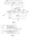
Figure 1 is a block schematic diagram of a phase locked loop comprising an apparatus in accordance with the invention coupled to a phase locked loop part; -
Figure 2 is a block schematic diagram of a sign detector; -
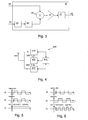
Figure 3 is a block schematic diagram of a scaling controller; -
Figure 4 is a block schematic diagram of a wireless communication device; -
Figure 5 is a diagram of waveforms without a phase shift; -
Figure 6 is a diagram of waveforms with a phase shift; and -
Figure 7 is a diagram of waveforms when the phase of the modulation is employed. - Referring to
Figure 1 , there is illustrated a phase lockedloop 500 comprising anapparatus 100 in accordance with the invention, and a phase lockedloop part 200 which is known in the prior art. - Describing first the phase locked
loop part 200, it comprises avariable frequency oscillator 240, such as a voltage controlled oscillator or a digitally controlled oscillator. Thevariable frequency oscillator 240 provides an oscillator signal at anoutput 260. Theoutput 260 is coupled to an input of adivider 250 for dividing the oscillator signal. The division ratio of thedivider 250 can be varied in response to a signal provided at aninput 255 of thedivider 250. Theinput 255 is thereby a first modulation point for modulating thevariable frequency oscillator 240 with a modulation signal. The divider provides the divided and modulated oscillator signal at an output which is coupled to a first input of aphase comparator 210. Asecond input 205 of thephase comparator 210 receives a reference signal generated by a reference oscillator (not illustrated), such as a crystal oscillator. Thephase comparator 210 provides an error signal at an output which is coupled to an input of afilter 220. The error signal is indicative of the phase difference between the reference signal and the divided and modulated oscillator signal. The filtered error signal is coupled to a first input of a summingstage 230. Asecond input 233 of the summingstage 230 also receives the modulation signal, and the summing stage provides the sum of the filtered error signal and the modulation signal at an output which is coupled to an input of thevariable frequency oscillator 240 for controlling its frequency. Thesecond input 233 of the summingstage 230 thus provides a second modulation point for modulating thevariable frequency oscillator 240. - The summing
stage 230 may be implemented in various ways. For example, for an analogue phase locked loop it may sum voltages, and for a digital phase locked loop it may sum digital codes. A further possibility is for the inputs of the summingstage 230 to directly drive independent varicaps, or capacitor banks, in which case the resulting sum is the sum of capacitance values. - In order to compensate for variations in the gain of the
variable frequency oscillator 240, the modulation signal can be scaled by ascaling stage 310 coupled to thesecond input 233 of the summingstage 230. The scalingstage 310 may be, for example, a variable gain amplifier or may be implemented in a digital processor. Thus the modulation signal to be applied to the second modulation point is provided at aninput 235 of thescaling stage 310, and the degree of scaling by the scalingstage 310 is determined by a scaling control signal coupled to a control input of thescaling stage 310. InFigure 1 thescaling stage 310 is shown as separate from theapparatus 100 and the phase lockedloop part 200, but in practice it may be incorporated into theapparatus 100 or into the phase lockedloop part 200. - Turning now to the
apparatus 100, it comprises asign detector 10 having aninput 12 for the modulation signal. Thesign detector 10 provides at an output an indication of whether the modulation signal and the phase of the modulation signal have the same sign, relative to, respectively, a first threshold value and a second threshold value. An embodiment of thesign detector 10 is described in detail below. - The
apparatus 100 also comprises a scalingcontroller 20 which has afirst input 40 coupled to the output of thesign detector 10, and asecond input 22 coupled to receive the error signal from the phase lockedloop part 200. As illustrated inFigure 1 , the error signal may be provided to theinput 22 from the output of thefilter 220. Alternatively, the error signal may be provided to theinput 22 from the input of thefilter 220; in this case separate filtering may be provided for the error signal supplied to theinput 22. The scalingcontroller 20 provides at an output 28 a scaling control signal, and theoutput 28 is coupled to the control input of thescaling stage 310. The scalingcontroller 20 is adapted to adjust the scaling control signal in response to the error signal, and is also adapted to adjust the scaling control signal only when the modulation signal and the phase of the modulation signal have the same sign, as indicated by thesign detector 10. An embodiment of the scalingcontroller 20 is described in detail below. - Before describing embodiments of the
sign detector 10 and the scalingcontroller 20, the principles underlying the invention will be described. The error signal u(s) of a phase locked loop may be expressed as
where s is the Laplace operator, k is the oscillator gain, Ko is a constant, L(s) is the open loop transfer function, and wm(s) is the modulation signal. Ideally, k=1, so 1-k represents the gain error. As an initial approximation, assume that L(s) is large, so that 1 + 1/L(s) = 1. Therefore,
- If the error signal u(s) has the same sign as the modulation signal wm, then the gain error 1-k is positive, which indicates that the oscillator gain is less than one, so is too small. If the error signal u(s) has the opposite sign to the modulation signal wm, then the gain error 1-k is negative, which indicates that the oscillator gain is greater than one, so is too large. It is apparent from equation (1) that

where the Laplace operator has been omitted because this is applicable in either the time domain or frequency domain. Thus it can be determined, from the sign of the error signal and the modulation signal, whether the gain is too small or too large by evaluating:
- The approximation that L(s) is large is valid at low frequencies where the loop gain is high. However, at high frequencies where the loop gain is lower it is possible that the error signal is delayed by 90 degrees with respect to the modulation signal. In this case, multiplying signals that are 90 degrees apart results in a zero average, and not in a valid indication of gain error.
- This problem is readily illustrated by means of waveform diagrams. In
Figures 5, 6 and7 , "sg" is an abbreviation for the sign function, wm(t) represents the modulation signal as a function of time t, u(t) represents the error signal as a function of time, and φm(t) represents the phase of the modulation signal as a function of time.Figure 5 illustrates a situation in which the modulation signal and the error signal are in-phase, resulting in the product v(t) of their signs being positive. Therefore, according to equation (2), the oscillator gain k is too small.Figure 6 illustrates a situation in which the modulation signal and the error signal are 90 degrees out of phase, resulting in the product v(t) of their signs alternating between positive and negative values, and which if averaged would have a mean value of zero. Therefore, in this case a valid indication of whether k is too large or too small is not generated. As the phase difference approaches 90 degrees, the indication decreases to zero and so becomes progressively unreliable. If the phase difference approaches 180 degrees, the error signal changes sign and an erroneous indication of whether k is too large or too small is generated. -
Figure 7 illustrates a situation in which the modulation signal and the error signal are 90 degrees out of phase, but now the phase φm(t) of the modulation signal, shown in trace (c), is employed according to the invention. The waveforms of sg(φm(t)) and sg(wm(t)) may be visualised as cosine and sine waves which have been limited. Trace (d) illustrates the sum of the signs of the modulation signal and the phase of the modulation signal; where the sign of wm(t) and φm(t) is different, the sum is zero, and where these signs are the same, the sum is either positive or negative. Trace (e) illustrates the waveform of trace (d) multiplied by the sign of the error signal u(t). Now, despite the 90 degree phase shift between the modulation signal and the error signal, a positive signal is generated periodically, and this has a positive mean value. Corresponding examples can be generated for other phase shifts, which demonstrate that a non-zero mean value results which can be used for compensation of the oscillator gain, including a phase shift of around 180 degrees. - Thus, by employing the phase of the modulation signal according to the invention, a valid indication can be generated of whether the gain k of the oscillator is too small or too large, independent of phase shift between the modulation signal and the error signal, and thus independent of modulation frequency. In this way, the invention is advantageous in providing a scheme for assessing and adjusting the value of k which is independent of the frequency content of the modulation signal and independent of the phase response of the phase locked loop.
- An embodiment of the
sign detector 10 will now be described in more detail, with reference toFigure 2 . Thesign detector 10 comprises afirst comparator 15 coupled to theinput 12 for comparing the modulation signal with the first threshold value, and for providing at an output of the comparator 15 a first sign signal indicative of whether the modulation signal is greater than or less than the first threshold. Preferably any DC component of the modulation signal is removed, in which case the first threshold value can be zero. The first sign signal provided at the output of thecomparator 15 is a bipolar signal, and preferably has a value +1 or -1 according to whether the modulation signal is greater than or less than the first threshold. - Also coupled to the
input 12 is aphase determination stage 16 for determining a phase signal indicative of the phase of the modulation signal. Thephase determination stage 16 may be, for example, an integrator. Alternatively, thephase determination stage 16 may be omitted and thesign detector 10 supplied with the phase signal on a further input (not illustrated). An output of thephase determination stage 16, or alternatively the further input, is coupled to an input of asecond comparator 19 for comparing the phase signal with the second threshold value, and for providing at an output of the comparator 19 a second sign signal indicative of whether the phase signal is greater than or less than the second threshold. Preferably any DC component of the phase signal is removed, in which case the second threshold value can be zero. The second sign signal provided at the output of thecomparator 19 is a bipolar signal, and preferably has a value +1 or -1 according to whether the phase signal is greater than or less than the second threshold. - The output of the
first comparator 15 and the output of thesecond comparator 19 are coupled to respective inputs of a summer 11 which sums the first and second sign signals and provides at an output an indication of whether the first and second sign signals have the same sign, thereby providing an indication of whether the modulation signal and the phase of the modulation signal have the same sign relative to their respective first and second threshold values. If the first and second sign signals can both have values +1 and -1, the indication at the output of the summer 11 can have values +2, 0 and -2. The value zero occurs when the modulation signal and the phase of the modulation signal have the different signs, and the values +2 and -2 occur when modulation signal and the phase of the modulation signal have the same sign. -
Figure 2 also illustratesoptional elements - An embodiment of the scaling
controller 20 will now be described in more detail, with reference toFigure 3 . The scalingcontroller 20 comprises athird comparator 24 for comparing the error signal provided at theinput 22 with a third threshold value, and for providing at an output of the comparator 24 a third sign signal indicative of whether the error signal is greater than or less than the third threshold. Preferably any DC component of the error signal is removed, in which case the third threshold value can be zero. The third sign signal provided at the output of thecomparator 24 is a bipolar signal, and preferably has a value +1 or -1 according to whether the error signal is greater than or less than the third threshold. - The output of the
comparator 24 is coupled to a first input of amultiplier 25, and theinput 40 is coupled to a second input of themultiplier 25. Themultiplier 25 multiplies the third sign signal by the indication of whether the modulation signal and the phase of the modulation signal have the same sign, which is provided at the output of the summer 11 of thesign detector 10. When the third sign signal can have values +1 and -1, and the indication provided at the output of the summer 11 can have the values +2, 0 and -2, the values resulting from multiplication by themultiplier 25 can have also the values +2, 0 and -2. The value zero occurs when the modulation signal and the phase of the modulation signal have the different signs, and the values +2 and -2 occur, dependent on the sign of the error signal, when modulation signal and the phase of the modulation signal have the same sign. The output of themultiplier 25 is coupled to theoutput 28 of the scalingcontrol stage 20 via afirst scaling stage 26, for example an amplifier, and afilter 27, which functions as an integrator, to provide the scaling control signal. While the output of themultiplier 25 provides a value of zero, the scaling control signal is also zero and so no adjustment is made, and the integrator holds the current value of the scaling control signal. - Optionally, the
sign detector 10 may comprise anoptional delay stage 13a and anoptional filter 14b either or both of which may be coupled between theinput 12 and thecomparator 15 to delay and/or filter the modulation signal. Likewise, optionally adelay stage 13b and/or afilter 14b may be coupled between thephase determination stage 16 and thecomparator 15 to delay and/or filter the phase signal. The delay stages 13a and 13b (together identified by reference numeral 13) andfilters apparatus 100 or phase lockedloop part 200 and to reduce noise. In particular, the modulation signal can be delayed by a period equivalent to the delay between a change in the modulation signal and a consequent change in the error signal. - Alternatively, the delay stages 13a and 13b may be located after, respectively, the first and
second comparators filters - Optionally, the scaling
controller 20 may comprise afilter 23 coupled between theinput 22 and thecomparator 24 for filtering the error signal to reduce noise. However, thefilter 23 may introduce a delay which may lead to instability unless further precautions are taken. In this case, thefilters - Referring to
Figure 4 , there is illustrated a block schematic diagram of awireless communication device 400, such as a mobile telephone, comprising atransmitter 410 and areceiver 420 coupled to anantenna 440. There is afrequency generator 430 which comprises the phase locked loop illustrated inFigure 1 , including theapparatus 100 in accordance with the invention and the phase lockedloop part 200, and a reference oscillator (not illustrated) coupled to theinput 205 of the phase lockedloop part 200 for generating the reference signal. There is abaseband processor 450 coupled tofrequency generator 430 for providing a modulation signal to thefrequency generator 430, coupled to thetransmitter 410 for controlling the transmitter, and coupled to thereceiver 420 for controlling thereceiver 420 and for processing received signals. Thefrequency generator 430 is coupled to thetransmitter 410 via theoutput 260 for providing a modulated carrier signal for transmission, and to thereceiver 420 for providing a local oscillator for use by thereceiver 420. - Although the invention has been described with reference to a phase locked loop which is equipped for two-point modulation, the
apparatus 100 may also be used to calibrate a phase locked loop that employs single point modulation, or that is unmodulated for the majority of time, with the modulation being supplied only when calibration of the oscillator gain is required. Similarly, the invention is not limited to use with a phase locked loop that comprises a divider, or specifically a divider having a variable division ratio. - The
apparatus 100, and in particular thesign detector 10 and scalingcontroller 20, described above may be implemented in analogue or digital hardware or in software executed by a processor. Other embodiments of thesign detector 10 and scalingcontroller 20 may be used. For example, although embodiments of thesign detector 10 and the scalingcontroller 20 have been described which use bipolar signals, alternatively these elements may be designed to process signals of other types, in particular multilevel signals, analogue signals, or monopolar signals. - In particular, the use of
comparators sign detector 10 of whether the modulation signal and the phase of the modulation signal have the same sign can have any form, such as an analogue signal or a digital value, and need not be a three level signal as described in relation to the embodiment ofFigure 2 . - The invention may be implemented using separate elements as illustrated in the drawings. However, it may equally be implemented using a single element such as an individual processor, digital signal processor (DSP) or central processing unit (CPU) providing the same functionality. Similarly, the invention could be implemented using a hard-wired circuit or circuits, such as an application-specific integrated circuit (ASIC), or by embedded software. Indeed, it can also be appreciated that the invention can be implemented using computer program code or computer software. The computer software or computer program code can be carried by a computer readable medium. The medium may be a physical storage medium such as a Read Only Memory (ROM) chip. Alternatively, it may be a disk such as a Digital Versatile Disk (DVD-ROM) or Compact Disk (CD-ROM). It could also be a signal such as an electronic signal over wires, an optical signal or a radio signal such as to a satellite or the like.
- From reading the present disclosure, other variations and modifications will be apparent to the skilled person. Such variations and modifications may involve equivalent and other features which are already known in the art of phase locked loops, and which may be used instead of, or in addition to, features already described herein.
- Although the appended claims are directed to particular combinations of features, it should be understood that the scope of the disclosure of the present invention also includes any novel feature or any novel combination of features disclosed herein either explicitly or implicitly or any generalisation thereof, whether or not it relates to the same invention as presently claimed in any claim and whether or not it mitigates any or all of the same technical problems as does the present invention.
- Features which are described in the context of separate embodiments may also be provided in combination in a single embodiment. Conversely, various features which are, for brevity, described in the context of a single embodiment, may also be provided separately or in any suitable subcombination.
- The applicant hereby gives notice that new claims may be formulated to such features and/or combinations of such features during the prosecution of the present application or of any further application derived therefrom.
- For the sake of completeness it is also stated that the term "comprising" does not exclude other elements or steps, the term "a" or "an" does not exclude a plurality, a single processor or other unit may fulfil the functions of several means recited in the claims and reference signs in the claims shall not be construed as limiting the scope of the claims.
Claims (19)
- Apparatus (100) for controlling a modulation signal for modulating a phase locked loop (200), the phase locked loop providing an error signal indicative of a phase error in the phase locked loop, the apparatus comprising:a scaling controller (20) for generating a scaling control signal dependent on the error signal for controlling scaling of the modulation signal; anda sign detector (10) for generating an indication of whether the sign of the modulation signal relative to a first threshold value and the sign of the phase of the modulation signal relative to a second threshold value are the same; wherein the scaling controller (20) is adapted to adjust the scaling control signal in response to the indication.
- Apparatus (100) as claimed in claim 1, wherein the scaling controller (20) is adapted to adjust the scaling control signal only when the modulation signal and the phase of the modulation signal have the same sign.
- Apparatus (100) as claimed in claim 1 or 2, wherein the sign detector (10) comprises:a first comparator (15) for generating a first bipolar signal indicative of the sign of the modulation signal relative to the first threshold value;a second comparator (19) for generating a second bipolar signal indicative of the sign of the phase of the modulation signal relative to the second threshold value; anda summer (11) for generating said indication by summing the first bipolar signal and the second bipolar signal.
- Apparatus (100) as claimed in any preceding claim, wherein the sign detector (10) comprises phase determination stage (16) for determining a phase signal indicative of the phase of the modulation signal.
- Apparatus (100) as claimed in any preceding claim, wherein the sign detector (10) comprises a delay stage (13) for delaying at least one of the first bipolar signal and the second bipolar signal.
- Apparatus (100) as claimed in any preceding claim, wherein the sign detector (10) comprises a first filter (14) arranged to filter at least one of the modulation signal and a phase signal indicative of the phase of the modulation signal.
- Apparatus (100) as claimed in any preceding claim, wherein the scaling controller (20) comprises:a third comparator (24) for generating a third bipolar signal indicative of the sign of the error signal relative to a third threshold value; anda multiplier (25) for multiplying the third bipolar signal by said indication.
- Apparatus (100) as claimed in claim 7, wherein the scaling controller (20) comprises a first scaling stage (26) coupled to an output of the multiplier (25) for controlling the magnitude of the scaling control signal.
- Apparatus (100) as claimed in claim 7 wherein the scaling controller (20) comprises a second filter (27) coupled to an output of the first scaling stage (26).
- Apparatus (100) as claimed in any preceding claim, wherein the scaling controller (20) comprises a third filter (23) for filtering the error signal.
- Apparatus (100) as claimed in any preceding claim, comprising a second scaling stage (310) for scaling the modulation signal in response to the scaling control signal.
- A phase locked loop (500) comprising:apparatus (100) as claimed in any preceding claim;a variable frequency oscillator (240) for generating an oscillator signal at an oscillator frequency;a phase comparator (210) for generating the error signal indicative of a phase difference between the oscillator signal and a reference signal;a loop filter (220) for filtering the error signal to provide a filtered error signal; anda coupling stage (230) for coupling the modulation signal, scaled in response to the scaling control signal, in combination with the filtered error signal to the variable frequency oscillator (240) for controlling the oscillator frequency.
- A phase locked loop (500) as claimed in claim 11, comprising a divider (250) for dividing the oscillator signal, and wherein the error signal is indicative of a phase difference between the divided oscillator signal and a reference signal.
- A phase locked loop (500) as claimed in claim 13, wherein the divider (250) is adapted to divide the oscillator signal using a variable division ratio, and the divider comprises an input (255) for varying the division ratio in response to the phase of the modulation signal.
- A phase locked loop (500) as claimed in claim 11, 13 or 14 when dependent on claim 3, wherein the delay introduced by the delay stage (13) corresponds to a delay between a change in the modulation signal and a consequent change in the error signal.
- A wireless communication device comprising a phase locked loop as claimed in any one of claims 11 to 15.
- A method for controlling a modulation signal for modulating a phase locked loop (200), the phase locked loop providing an error signal indicative of a phase error in the phase locked loop, the method comprising:generating a scaling control signal dependent on the error signal for controlling scaling of the modulation signal;generating an indication of whether the sign of the modulation signal relativeto a first threshold value and the sign of the phase of the modulation signalrelative to a second threshold value are the same; andadjusting the scaling control signal in response to the indication.
- A method as claimed in claim 17, comprising adjusting the scaling control signal only when the modulation signal and the phase of the modulation signal have the same sign.
- Computer program code adapted to perform the method of claim 17 or 18 when executed by a processor.
Priority Applications (1)
| Application Number | Priority Date | Filing Date | Title |
|---|---|---|---|
| EP09000654A EP2083515B1 (en) | 2008-01-22 | 2009-01-19 | Phase locked loop calibration |
Applications Claiming Priority (2)
| Application Number | Priority Date | Filing Date | Title |
|---|---|---|---|
| EP08100724 | 2008-01-22 | ||
| EP09000654A EP2083515B1 (en) | 2008-01-22 | 2009-01-19 | Phase locked loop calibration |
Publications (3)
| Publication Number | Publication Date |
|---|---|
| EP2083515A2 true EP2083515A2 (en) | 2009-07-29 |
| EP2083515A3 EP2083515A3 (en) | 2012-02-01 |
| EP2083515B1 EP2083515B1 (en) | 2013-01-02 |
Family
ID=40627004
Family Applications (2)
| Application Number | Title | Priority Date | Filing Date |
|---|---|---|---|
| EP08290442A Withdrawn EP2083514A3 (en) | 2008-01-22 | 2008-05-12 | Signal generation |
| EP09000654A Active EP2083515B1 (en) | 2008-01-22 | 2009-01-19 | Phase locked loop calibration |
Family Applications Before (1)
| Application Number | Title | Priority Date | Filing Date |
|---|---|---|---|
| EP08290442A Withdrawn EP2083514A3 (en) | 2008-01-22 | 2008-05-12 | Signal generation |
Country Status (2)
| Country | Link |
|---|---|
| US (1) | US8290108B2 (en) |
| EP (2) | EP2083514A3 (en) |
Families Citing this family (3)
| Publication number | Priority date | Publication date | Assignee | Title |
|---|---|---|---|---|
| JP2019097080A (en) * | 2017-11-24 | 2019-06-20 | 富士通株式会社 | Signal regeneration circuit, optical module and signal regeneration method |
| KR102474578B1 (en) * | 2018-01-08 | 2022-12-05 | 삼성전자주식회사 | Semiconductor device and method for operating semiconductor device |
| EP3800787A1 (en) * | 2019-10-02 | 2021-04-07 | Imec VZW | A method of calibrating and a calibration circuit for a two-point modulation phase locked loop |
Citations (3)
| Publication number | Priority date | Publication date | Assignee | Title |
|---|---|---|---|---|
| US6670861B1 (en) | 2002-08-29 | 2003-12-30 | Analog Devices, Inc. | Method of modulation gain calibration and system thereof |
| WO2004034564A2 (en) | 2002-09-06 | 2004-04-22 | Telefonaktiebolaget Lm Ericsson (Publ) | Trimming of a two point phase modulator |
| US20070103240A1 (en) | 2004-08-12 | 2007-05-10 | Staszewski Robert B | Gain Calibration of a Digital Controlled Oscillator |
Family Cites Families (4)
| Publication number | Priority date | Publication date | Assignee | Title |
|---|---|---|---|---|
| CA2281522C (en) * | 1999-09-10 | 2004-12-07 | Philsar Electronics Inc. | Delta-sigma based two-point angle modulation scheme |
| US8267683B2 (en) | 2005-07-27 | 2012-09-18 | Shofu Inc. | Apparatus for forming layered object |
| US7420433B2 (en) * | 2005-11-17 | 2008-09-02 | Analog Devices, Inc. | Phase lock loop RF modulator system |
| US7728690B2 (en) * | 2007-10-19 | 2010-06-01 | Qualcomm, Incorporated | Method and apparatus for compensating for tuning nonlinearity of an oscillator |
-
2008
- 2008-05-12 EP EP08290442A patent/EP2083514A3/en not_active Withdrawn
-
2009
- 2009-01-19 EP EP09000654A patent/EP2083515B1/en active Active
- 2009-01-22 US US12/357,918 patent/US8290108B2/en active Active
Patent Citations (3)
| Publication number | Priority date | Publication date | Assignee | Title |
|---|---|---|---|---|
| US6670861B1 (en) | 2002-08-29 | 2003-12-30 | Analog Devices, Inc. | Method of modulation gain calibration and system thereof |
| WO2004034564A2 (en) | 2002-09-06 | 2004-04-22 | Telefonaktiebolaget Lm Ericsson (Publ) | Trimming of a two point phase modulator |
| US20070103240A1 (en) | 2004-08-12 | 2007-05-10 | Staszewski Robert B | Gain Calibration of a Digital Controlled Oscillator |
Also Published As
| Publication number | Publication date |
|---|---|
| EP2083515A3 (en) | 2012-02-01 |
| US20090190709A1 (en) | 2009-07-30 |
| EP2083514A2 (en) | 2009-07-29 |
| US8290108B2 (en) | 2012-10-16 |
| EP2083515B1 (en) | 2013-01-02 |
| EP2083514A3 (en) | 2012-10-31 |
Similar Documents
| Publication | Publication Date | Title |
|---|---|---|
| US8364098B2 (en) | PLL calibration | |
| US8750441B2 (en) | Signal cancellation to reduce phase noise, period jitter, and other contamination in local oscillator, frequency timing, or other timing generators or signal sources | |
| US8315559B2 (en) | Transmitter and control method for transmitting and calibrating a phase signal and an amplitude signal | |
| US20060055466A1 (en) | Modulator and correction method thereof | |
| CN100530938C (en) | Wide-band modulation PLL, timing error correction system, method and adjusting method | |
| AU1216897A (en) | Digital calibration of a transceiver | |
| US8391814B2 (en) | Power control loop, transmitter with the power control loop and method for controlling output power of a transmitter device | |
| US7916804B2 (en) | Method and system for a fast-switching phase-locked loop using a direct digital frequency synthesizer | |
| EP2083515B1 (en) | Phase locked loop calibration | |
| US7991102B2 (en) | Signal generating apparatus and method thereof | |
| US20100323638A1 (en) | Phase corrector and phase correction method | |
| TWI901755B (en) | Electronic device and method of operating electronic device | |
| US20060209987A1 (en) | Receiver and its adjustment system and method | |
| EP2144364A1 (en) | Feedback system | |
| JP5042774B2 (en) | FSK modulation circuit | |
| CN114448427B (en) | Calibration circuit, method, chip and electronic device for phase-locked loop | |
| KR970002886B1 (en) | FM demodulation circuit | |
| JP4815572B2 (en) | Compensated high-speed PLL circuit | |
| CN117639814A (en) | A signal processing circuit, signal processing method and electronic equipment | |
| JP3672913B2 (en) | Oscillation frequency correction circuit for portable radio | |
| WO2003043212A1 (en) | Receiver and its tracking adjusting method | |
| JP2008035073A (en) | Quadrature modulator | |
| EP1450495A1 (en) | Receiver and its tracking adjusting method | |
| JP2006203614A (en) | Automatic frequency controller | |
| JPH01290318A (en) | Frequency correction circuit |
Legal Events
| Date | Code | Title | Description |
|---|---|---|---|
| PUAI | Public reference made under article 153(3) epc to a published international application that has entered the european phase |
Free format text: ORIGINAL CODE: 0009012 |
|
| AK | Designated contracting states |
Kind code of ref document: A2 Designated state(s): AT BE BG CH CY CZ DE DK EE ES FI FR GB GR HR HU IE IS IT LI LT LU LV MC MK MT NL NO PL PT RO SE SI SK TR |
|
| AX | Request for extension of the european patent |
Extension state: AL BA RS |
|
| RAP1 | Party data changed (applicant data changed or rights of an application transferred) |
Owner name: ST-ERICSSON SA |
|
| PUAL | Search report despatched |
Free format text: ORIGINAL CODE: 0009013 |
|
| AK | Designated contracting states |
Kind code of ref document: A3 Designated state(s): AT BE BG CH CY CZ DE DK EE ES FI FR GB GR HR HU IE IS IT LI LT LU LV MC MK MT NL NO PL PT RO SE SI SK TR |
|
| AX | Request for extension of the european patent |
Extension state: AL BA RS |
|
| RIC1 | Information provided on ipc code assigned before grant |
Ipc: H03C 3/09 20060101AFI20111227BHEP |
|
| 17P | Request for examination filed |
Effective date: 20120719 |
|
| GRAP | Despatch of communication of intention to grant a patent |
Free format text: ORIGINAL CODE: EPIDOSNIGR1 |
|
| AKX | Designation fees paid |
Designated state(s): AT BE BG CH CY CZ DE DK EE ES FI FR GB GR HR HU IE IS IT LI LT LU LV MC MK MT NL NO PL PT RO SE SI SK TR |
|
| GRAS | Grant fee paid |
Free format text: ORIGINAL CODE: EPIDOSNIGR3 |
|
| GRAA | (expected) grant |
Free format text: ORIGINAL CODE: 0009210 |
|
| AK | Designated contracting states |
Kind code of ref document: B1 Designated state(s): AT BE BG CH CY CZ DE DK EE ES FI FR GB GR HR HU IE IS IT LI LT LU LV MC MK MT NL NO PL PT RO SE SI SK TR |
|
| REG | Reference to a national code |
Ref country code: GB Ref legal event code: FG4D |
|
| REG | Reference to a national code |
Ref country code: CH Ref legal event code: EP Ref country code: AT Ref legal event code: REF Ref document number: 592075 Country of ref document: AT Kind code of ref document: T Effective date: 20130115 |
|
| REG | Reference to a national code |
Ref country code: IE Ref legal event code: FG4D |
|
| REG | Reference to a national code |
Ref country code: DE Ref legal event code: R096 Ref document number: 602009012354 Country of ref document: DE Effective date: 20130307 |
|
| REG | Reference to a national code |
Ref country code: AT Ref legal event code: MK05 Ref document number: 592075 Country of ref document: AT Kind code of ref document: T Effective date: 20130102 |
|
| REG | Reference to a national code |
Ref country code: NL Ref legal event code: VDEP Effective date: 20130102 |
|
| PG25 | Lapsed in a contracting state [announced via postgrant information from national office to epo] |
Ref country code: SI Free format text: LAPSE BECAUSE OF FAILURE TO SUBMIT A TRANSLATION OF THE DESCRIPTION OR TO PAY THE FEE WITHIN THE PRESCRIBED TIME-LIMIT Effective date: 20130102 |
|
| REG | Reference to a national code |
Ref country code: LT Ref legal event code: MG4D |
|
| PG25 | Lapsed in a contracting state [announced via postgrant information from national office to epo] |
Ref country code: CZ Free format text: LAPSE BECAUSE OF FAILURE TO SUBMIT A TRANSLATION OF THE DESCRIPTION OR TO PAY THE FEE WITHIN THE PRESCRIBED TIME-LIMIT Effective date: 20130102 Ref country code: BG Free format text: LAPSE BECAUSE OF FAILURE TO SUBMIT A TRANSLATION OF THE DESCRIPTION OR TO PAY THE FEE WITHIN THE PRESCRIBED TIME-LIMIT Effective date: 20130402 Ref country code: NO Free format text: LAPSE BECAUSE OF FAILURE TO SUBMIT A TRANSLATION OF THE DESCRIPTION OR TO PAY THE FEE WITHIN THE PRESCRIBED TIME-LIMIT Effective date: 20130402 Ref country code: SE Free format text: LAPSE BECAUSE OF FAILURE TO SUBMIT A TRANSLATION OF THE DESCRIPTION OR TO PAY THE FEE WITHIN THE PRESCRIBED TIME-LIMIT Effective date: 20130102 Ref country code: AT Free format text: LAPSE BECAUSE OF FAILURE TO SUBMIT A TRANSLATION OF THE DESCRIPTION OR TO PAY THE FEE WITHIN THE PRESCRIBED TIME-LIMIT Effective date: 20130102 Ref country code: BE Free format text: LAPSE BECAUSE OF FAILURE TO SUBMIT A TRANSLATION OF THE DESCRIPTION OR TO PAY THE FEE WITHIN THE PRESCRIBED TIME-LIMIT Effective date: 20130102 Ref country code: IS Free format text: LAPSE BECAUSE OF FAILURE TO SUBMIT A TRANSLATION OF THE DESCRIPTION OR TO PAY THE FEE WITHIN THE PRESCRIBED TIME-LIMIT Effective date: 20130502 Ref country code: LT Free format text: LAPSE BECAUSE OF FAILURE TO SUBMIT A TRANSLATION OF THE DESCRIPTION OR TO PAY THE FEE WITHIN THE PRESCRIBED TIME-LIMIT Effective date: 20130102 Ref country code: ES Free format text: LAPSE BECAUSE OF FAILURE TO SUBMIT A TRANSLATION OF THE DESCRIPTION OR TO PAY THE FEE WITHIN THE PRESCRIBED TIME-LIMIT Effective date: 20130413 |
|
| PG25 | Lapsed in a contracting state [announced via postgrant information from national office to epo] |
Ref country code: NL Free format text: LAPSE BECAUSE OF FAILURE TO SUBMIT A TRANSLATION OF THE DESCRIPTION OR TO PAY THE FEE WITHIN THE PRESCRIBED TIME-LIMIT Effective date: 20130102 Ref country code: LV Free format text: LAPSE BECAUSE OF FAILURE TO SUBMIT A TRANSLATION OF THE DESCRIPTION OR TO PAY THE FEE WITHIN THE PRESCRIBED TIME-LIMIT Effective date: 20130102 Ref country code: PL Free format text: LAPSE BECAUSE OF FAILURE TO SUBMIT A TRANSLATION OF THE DESCRIPTION OR TO PAY THE FEE WITHIN THE PRESCRIBED TIME-LIMIT Effective date: 20130102 Ref country code: FI Free format text: LAPSE BECAUSE OF FAILURE TO SUBMIT A TRANSLATION OF THE DESCRIPTION OR TO PAY THE FEE WITHIN THE PRESCRIBED TIME-LIMIT Effective date: 20130102 Ref country code: GR Free format text: LAPSE BECAUSE OF FAILURE TO SUBMIT A TRANSLATION OF THE DESCRIPTION OR TO PAY THE FEE WITHIN THE PRESCRIBED TIME-LIMIT Effective date: 20130403 Ref country code: PT Free format text: LAPSE BECAUSE OF FAILURE TO SUBMIT A TRANSLATION OF THE DESCRIPTION OR TO PAY THE FEE WITHIN THE PRESCRIBED TIME-LIMIT Effective date: 20130502 Ref country code: MC Free format text: LAPSE BECAUSE OF NON-PAYMENT OF DUE FEES Effective date: 20130131 |
|
| REG | Reference to a national code |
Ref country code: CH Ref legal event code: PL |
|
| PG25 | Lapsed in a contracting state [announced via postgrant information from national office to epo] |
Ref country code: HR Free format text: LAPSE BECAUSE OF FAILURE TO SUBMIT A TRANSLATION OF THE DESCRIPTION OR TO PAY THE FEE WITHIN THE PRESCRIBED TIME-LIMIT Effective date: 20130102 |
|
| REG | Reference to a national code |
Ref country code: IE Ref legal event code: MM4A |
|
| PG25 | Lapsed in a contracting state [announced via postgrant information from national office to epo] |
Ref country code: EE Free format text: LAPSE BECAUSE OF FAILURE TO SUBMIT A TRANSLATION OF THE DESCRIPTION OR TO PAY THE FEE WITHIN THE PRESCRIBED TIME-LIMIT Effective date: 20130102 Ref country code: DK Free format text: LAPSE BECAUSE OF FAILURE TO SUBMIT A TRANSLATION OF THE DESCRIPTION OR TO PAY THE FEE WITHIN THE PRESCRIBED TIME-LIMIT Effective date: 20130102 Ref country code: RO Free format text: LAPSE BECAUSE OF FAILURE TO SUBMIT A TRANSLATION OF THE DESCRIPTION OR TO PAY THE FEE WITHIN THE PRESCRIBED TIME-LIMIT Effective date: 20130102 Ref country code: LI Free format text: LAPSE BECAUSE OF NON-PAYMENT OF DUE FEES Effective date: 20130131 Ref country code: CH Free format text: LAPSE BECAUSE OF NON-PAYMENT OF DUE FEES Effective date: 20130131 Ref country code: SK Free format text: LAPSE BECAUSE OF FAILURE TO SUBMIT A TRANSLATION OF THE DESCRIPTION OR TO PAY THE FEE WITHIN THE PRESCRIBED TIME-LIMIT Effective date: 20130102 |
|
| PLBE | No opposition filed within time limit |
Free format text: ORIGINAL CODE: 0009261 |
|
| STAA | Information on the status of an ep patent application or granted ep patent |
Free format text: STATUS: NO OPPOSITION FILED WITHIN TIME LIMIT |
|
| PG25 | Lapsed in a contracting state [announced via postgrant information from national office to epo] |
Ref country code: CY Free format text: LAPSE BECAUSE OF FAILURE TO SUBMIT A TRANSLATION OF THE DESCRIPTION OR TO PAY THE FEE WITHIN THE PRESCRIBED TIME-LIMIT Effective date: 20130102 |
|
| 26N | No opposition filed |
Effective date: 20131003 |
|
| REG | Reference to a national code |
Ref country code: FR Ref legal event code: ST Effective date: 20131108 |
|
| PG25 | Lapsed in a contracting state [announced via postgrant information from national office to epo] |
Ref country code: IT Free format text: LAPSE BECAUSE OF FAILURE TO SUBMIT A TRANSLATION OF THE DESCRIPTION OR TO PAY THE FEE WITHIN THE PRESCRIBED TIME-LIMIT Effective date: 20130102 |
|
| REG | Reference to a national code |
Ref country code: DE Ref legal event code: R097 Ref document number: 602009012354 Country of ref document: DE Effective date: 20131003 |
|
| PG25 | Lapsed in a contracting state [announced via postgrant information from national office to epo] |
Ref country code: FR Free format text: LAPSE BECAUSE OF NON-PAYMENT OF DUE FEES Effective date: 20130304 Ref country code: IE Free format text: LAPSE BECAUSE OF NON-PAYMENT OF DUE FEES Effective date: 20130119 |
|
| PG25 | Lapsed in a contracting state [announced via postgrant information from national office to epo] |
Ref country code: MT Free format text: LAPSE BECAUSE OF FAILURE TO SUBMIT A TRANSLATION OF THE DESCRIPTION OR TO PAY THE FEE WITHIN THE PRESCRIBED TIME-LIMIT Effective date: 20130102 |
|
| PG25 | Lapsed in a contracting state [announced via postgrant information from national office to epo] |
Ref country code: TR Free format text: LAPSE BECAUSE OF FAILURE TO SUBMIT A TRANSLATION OF THE DESCRIPTION OR TO PAY THE FEE WITHIN THE PRESCRIBED TIME-LIMIT Effective date: 20130102 |
|
| PG25 | Lapsed in a contracting state [announced via postgrant information from national office to epo] |
Ref country code: HU Free format text: LAPSE BECAUSE OF FAILURE TO SUBMIT A TRANSLATION OF THE DESCRIPTION OR TO PAY THE FEE WITHIN THE PRESCRIBED TIME-LIMIT; INVALID AB INITIO Effective date: 20090119 Ref country code: MK Free format text: LAPSE BECAUSE OF FAILURE TO SUBMIT A TRANSLATION OF THE DESCRIPTION OR TO PAY THE FEE WITHIN THE PRESCRIBED TIME-LIMIT Effective date: 20130102 Ref country code: LU Free format text: LAPSE BECAUSE OF NON-PAYMENT OF DUE FEES Effective date: 20130119 |
|
| REG | Reference to a national code |
Ref country code: DE Ref legal event code: R082 Ref document number: 602009012354 Country of ref document: DE Representative=s name: GRUENECKER PATENT- UND RECHTSANWAELTE PARTG MB, DE Ref country code: DE Ref legal event code: R081 Ref document number: 602009012354 Country of ref document: DE Owner name: OCT CIRCUIT TECHNOLOGIES INTERNATIONAL LTD., IE Free format text: FORMER OWNER: ST-ERICSSON SA, PLAN-LES-OUATES, CH |
|
| REG | Reference to a national code |
Ref country code: GB Ref legal event code: 732E Free format text: REGISTERED BETWEEN 20210722 AND 20210728 |
|
| REG | Reference to a national code |
Ref country code: GB Ref legal event code: 732E Free format text: REGISTERED BETWEEN 20210805 AND 20210811 |
|
| PGFP | Annual fee paid to national office [announced via postgrant information from national office to epo] |
Ref country code: GB Payment date: 20260127 Year of fee payment: 18 |
|
| PGFP | Annual fee paid to national office [announced via postgrant information from national office to epo] |
Ref country code: DE Payment date: 20260128 Year of fee payment: 18 |