EP2083328A1 - Grazing incidence collector for laser produced plasma sources - Google Patents
Grazing incidence collector for laser produced plasma sources Download PDFInfo
- Publication number
- EP2083328A1 EP2083328A1 EP08001536A EP08001536A EP2083328A1 EP 2083328 A1 EP2083328 A1 EP 2083328A1 EP 08001536 A EP08001536 A EP 08001536A EP 08001536 A EP08001536 A EP 08001536A EP 2083328 A1 EP2083328 A1 EP 2083328A1
- Authority
- EP
- European Patent Office
- Prior art keywords
- collector
- mirrors
- source
- mirror
- produced plasma
- Prior art date
- Legal status (The legal status is an assumption and is not a legal conclusion. Google has not performed a legal analysis and makes no representation as to the accuracy of the status listed.)
- Granted
Links
- 238000009304 pastoral farming Methods 0.000 title claims abstract description 32
- 230000003287 optical effect Effects 0.000 claims abstract description 67
- 230000005855 radiation Effects 0.000 claims abstract description 23
- 239000000446 fuel Substances 0.000 claims abstract description 16
- 238000001900 extreme ultraviolet lithography Methods 0.000 claims abstract description 7
- 230000001154 acute effect Effects 0.000 claims abstract description 3
- 238000005304 joining Methods 0.000 claims abstract description 3
- 239000010410 layer Substances 0.000 claims description 58
- 238000000576 coating method Methods 0.000 claims description 21
- 239000011248 coating agent Substances 0.000 claims description 20
- 230000000116 mitigating effect Effects 0.000 claims description 18
- 238000005323 electroforming Methods 0.000 claims description 16
- 239000000463 material Substances 0.000 claims description 16
- 238000000034 method Methods 0.000 claims description 15
- 239000002184 metal Substances 0.000 claims description 14
- 229910052751 metal Inorganic materials 0.000 claims description 14
- 229910052750 molybdenum Inorganic materials 0.000 claims description 13
- 229910052763 palladium Inorganic materials 0.000 claims description 13
- 229910045601 alloy Inorganic materials 0.000 claims description 12
- 239000000956 alloy Substances 0.000 claims description 12
- 229910052737 gold Inorganic materials 0.000 claims description 12
- 238000004519 manufacturing process Methods 0.000 claims description 12
- 230000001902 propagating effect Effects 0.000 claims description 12
- 229910052707 ruthenium Inorganic materials 0.000 claims description 11
- 230000003628 erosive effect Effects 0.000 claims description 10
- 229910052741 iridium Inorganic materials 0.000 claims description 10
- 229910052697 platinum Inorganic materials 0.000 claims description 10
- 229910052703 rhodium Inorganic materials 0.000 claims description 10
- 239000012530 fluid Substances 0.000 claims description 9
- 238000001816 cooling Methods 0.000 claims description 8
- 238000007516 diamond turning Methods 0.000 claims description 8
- 230000008569 process Effects 0.000 claims description 8
- 230000003746 surface roughness Effects 0.000 claims description 8
- 229910052802 copper Inorganic materials 0.000 claims description 7
- 238000010438 heat treatment Methods 0.000 claims description 7
- 229910052759 nickel Inorganic materials 0.000 claims description 7
- 239000000758 substrate Substances 0.000 claims description 6
- 230000000694 effects Effects 0.000 claims description 5
- 150000002739 metals Chemical class 0.000 claims description 5
- 239000002114 nanocomposite Substances 0.000 claims description 5
- 238000000926 separation method Methods 0.000 claims description 5
- 229910003266 NiCo Inorganic materials 0.000 claims description 4
- 239000003302 ferromagnetic material Substances 0.000 claims description 4
- 239000011241 protective layer Substances 0.000 claims description 4
- 230000004888 barrier function Effects 0.000 claims description 3
- 230000008878 coupling Effects 0.000 claims description 3
- 238000010168 coupling process Methods 0.000 claims description 3
- 238000005859 coupling reaction Methods 0.000 claims description 3
- 230000000873 masking effect Effects 0.000 claims description 3
- 238000005459 micromachining Methods 0.000 claims description 3
- 238000007747 plating Methods 0.000 claims description 3
- 230000001678 irradiating effect Effects 0.000 claims description 2
- 238000005498 polishing Methods 0.000 claims description 2
- 238000003384 imaging method Methods 0.000 abstract description 6
- 238000001459 lithography Methods 0.000 abstract description 2
- 239000010949 copper Substances 0.000 description 12
- 239000010931 gold Substances 0.000 description 12
- 150000002500 ions Chemical class 0.000 description 9
- 230000008901 benefit Effects 0.000 description 6
- 238000000151 deposition Methods 0.000 description 6
- 239000002245 particle Substances 0.000 description 6
- 230000008021 deposition Effects 0.000 description 5
- 238000002310 reflectometry Methods 0.000 description 5
- 229910017709 Ni Co Inorganic materials 0.000 description 4
- 229910003267 Ni-Co Inorganic materials 0.000 description 4
- 229910003262 Ni‐Co Inorganic materials 0.000 description 4
- 239000002356 single layer Substances 0.000 description 4
- 238000004140 cleaning Methods 0.000 description 3
- 230000005291 magnetic effect Effects 0.000 description 3
- 230000010076 replication Effects 0.000 description 3
- 238000009826 distribution Methods 0.000 description 2
- 239000002086 nanomaterial Substances 0.000 description 2
- 230000007935 neutral effect Effects 0.000 description 2
- 229910052758 niobium Inorganic materials 0.000 description 2
- 150000004767 nitrides Chemical class 0.000 description 2
- 238000002360 preparation method Methods 0.000 description 2
- 230000001681 protective effect Effects 0.000 description 2
- 238000004544 sputter deposition Methods 0.000 description 2
- 229910052726 zirconium Inorganic materials 0.000 description 2
- RYGMFSIKBFXOCR-UHFFFAOYSA-N Copper Chemical compound [Cu] RYGMFSIKBFXOCR-UHFFFAOYSA-N 0.000 description 1
- 241000446313 Lamella Species 0.000 description 1
- 229910052782 aluminium Inorganic materials 0.000 description 1
- 230000005540 biological transmission Effects 0.000 description 1
- 229910010293 ceramic material Inorganic materials 0.000 description 1
- 230000008859 change Effects 0.000 description 1
- 238000011109 contamination Methods 0.000 description 1
- 230000003247 decreasing effect Effects 0.000 description 1
- 238000005137 deposition process Methods 0.000 description 1
- 238000010586 diagram Methods 0.000 description 1
- 238000001704 evaporation Methods 0.000 description 1
- 230000008020 evaporation Effects 0.000 description 1
- 230000004907 flux Effects 0.000 description 1
- PCHJSUWPFVWCPO-UHFFFAOYSA-N gold Chemical compound [Au] PCHJSUWPFVWCPO-UHFFFAOYSA-N 0.000 description 1
- 150000004678 hydrides Chemical class 0.000 description 1
- 230000003116 impacting effect Effects 0.000 description 1
- 238000010849 ion bombardment Methods 0.000 description 1
- 239000000203 mixture Substances 0.000 description 1
- 230000000704 physical effect Effects 0.000 description 1
- 239000011253 protective coating Substances 0.000 description 1
- 238000005546 reactive sputtering Methods 0.000 description 1
- 230000002829 reductive effect Effects 0.000 description 1
- 238000001228 spectrum Methods 0.000 description 1
- 229910052718 tin Inorganic materials 0.000 description 1
Images


Classifications
-
- G—PHYSICS
- G03—PHOTOGRAPHY; CINEMATOGRAPHY; ANALOGOUS TECHNIQUES USING WAVES OTHER THAN OPTICAL WAVES; ELECTROGRAPHY; HOLOGRAPHY
- G03F—PHOTOMECHANICAL PRODUCTION OF TEXTURED OR PATTERNED SURFACES, e.g. FOR PRINTING, FOR PROCESSING OF SEMICONDUCTOR DEVICES; MATERIALS THEREFOR; ORIGINALS THEREFOR; APPARATUS SPECIALLY ADAPTED THEREFOR
- G03F7/00—Photomechanical, e.g. photolithographic, production of textured or patterned surfaces, e.g. printing surfaces; Materials therefor, e.g. comprising photoresists; Apparatus specially adapted therefor
- G03F7/70—Microphotolithographic exposure; Apparatus therefor
- G03F7/708—Construction of apparatus, e.g. environment aspects, hygiene aspects or materials
- G03F7/70908—Hygiene, e.g. preventing apparatus pollution, mitigating effect of pollution or removing pollutants from apparatus
- G03F7/70916—Pollution mitigation, i.e. mitigating effect of contamination or debris, e.g. foil traps
-
- B—PERFORMING OPERATIONS; TRANSPORTING
- B82—NANOTECHNOLOGY
- B82Y—SPECIFIC USES OR APPLICATIONS OF NANOSTRUCTURES; MEASUREMENT OR ANALYSIS OF NANOSTRUCTURES; MANUFACTURE OR TREATMENT OF NANOSTRUCTURES
- B82Y10/00—Nanotechnology for information processing, storage or transmission, e.g. quantum computing or single electron logic
-
- G—PHYSICS
- G03—PHOTOGRAPHY; CINEMATOGRAPHY; ANALOGOUS TECHNIQUES USING WAVES OTHER THAN OPTICAL WAVES; ELECTROGRAPHY; HOLOGRAPHY
- G03F—PHOTOMECHANICAL PRODUCTION OF TEXTURED OR PATTERNED SURFACES, e.g. FOR PRINTING, FOR PROCESSING OF SEMICONDUCTOR DEVICES; MATERIALS THEREFOR; ORIGINALS THEREFOR; APPARATUS SPECIALLY ADAPTED THEREFOR
- G03F7/00—Photomechanical, e.g. photolithographic, production of textured or patterned surfaces, e.g. printing surfaces; Materials therefor, e.g. comprising photoresists; Apparatus specially adapted therefor
- G03F7/70—Microphotolithographic exposure; Apparatus therefor
- G03F7/70008—Production of exposure light, i.e. light sources
- G03F7/70033—Production of exposure light, i.e. light sources by plasma extreme ultraviolet [EUV] sources
-
- G—PHYSICS
- G03—PHOTOGRAPHY; CINEMATOGRAPHY; ANALOGOUS TECHNIQUES USING WAVES OTHER THAN OPTICAL WAVES; ELECTROGRAPHY; HOLOGRAPHY
- G03F—PHOTOMECHANICAL PRODUCTION OF TEXTURED OR PATTERNED SURFACES, e.g. FOR PRINTING, FOR PROCESSING OF SEMICONDUCTOR DEVICES; MATERIALS THEREFOR; ORIGINALS THEREFOR; APPARATUS SPECIALLY ADAPTED THEREFOR
- G03F7/00—Photomechanical, e.g. photolithographic, production of textured or patterned surfaces, e.g. printing surfaces; Materials therefor, e.g. comprising photoresists; Apparatus specially adapted therefor
- G03F7/70—Microphotolithographic exposure; Apparatus therefor
- G03F7/70058—Mask illumination systems
- G03F7/7015—Details of optical elements
- G03F7/70166—Capillary or channel elements, e.g. nested extreme ultraviolet [EUV] mirrors or shells, optical fibers or light guides
-
- G—PHYSICS
- G21—NUCLEAR PHYSICS; NUCLEAR ENGINEERING
- G21K—TECHNIQUES FOR HANDLING PARTICLES OR IONISING RADIATION NOT OTHERWISE PROVIDED FOR; IRRADIATION DEVICES; GAMMA RAY OR X-RAY MICROSCOPES
- G21K1/00—Arrangements for handling particles or ionising radiation, e.g. focusing or moderating
- G21K1/06—Arrangements for handling particles or ionising radiation, e.g. focusing or moderating using diffraction, refraction or reflection, e.g. monochromators
- G21K1/062—Devices having a multilayer structure
-
- G—PHYSICS
- G21—NUCLEAR PHYSICS; NUCLEAR ENGINEERING
- G21K—TECHNIQUES FOR HANDLING PARTICLES OR IONISING RADIATION NOT OTHERWISE PROVIDED FOR; IRRADIATION DEVICES; GAMMA RAY OR X-RAY MICROSCOPES
- G21K1/00—Arrangements for handling particles or ionising radiation, e.g. focusing or moderating
- G21K1/06—Arrangements for handling particles or ionising radiation, e.g. focusing or moderating using diffraction, refraction or reflection, e.g. monochromators
- G21K1/067—Arrangements for handling particles or ionising radiation, e.g. focusing or moderating using diffraction, refraction or reflection, e.g. monochromators using surface reflection, e.g. grazing incidence mirrors, gratings
-
- H—ELECTRICITY
- H05—ELECTRIC TECHNIQUES NOT OTHERWISE PROVIDED FOR
- H05G—X-RAY TECHNIQUE
- H05G2/00—Apparatus or processes specially adapted for producing X-rays, not involving X-ray tubes, e.g. involving generation of a plasma
- H05G2/001—X-ray radiation generated from plasma
- H05G2/003—X-ray radiation generated from plasma being produced from a liquid or gas
-
- G—PHYSICS
- G21—NUCLEAR PHYSICS; NUCLEAR ENGINEERING
- G21K—TECHNIQUES FOR HANDLING PARTICLES OR IONISING RADIATION NOT OTHERWISE PROVIDED FOR; IRRADIATION DEVICES; GAMMA RAY OR X-RAY MICROSCOPES
- G21K2201/00—Arrangements for handling radiation or particles
- G21K2201/06—Arrangements for handling radiation or particles using diffractive, refractive or reflecting elements
- G21K2201/061—Arrangements for handling radiation or particles using diffractive, refractive or reflecting elements characterised by a multilayer structure
-
- G—PHYSICS
- G21—NUCLEAR PHYSICS; NUCLEAR ENGINEERING
- G21K—TECHNIQUES FOR HANDLING PARTICLES OR IONISING RADIATION NOT OTHERWISE PROVIDED FOR; IRRADIATION DEVICES; GAMMA RAY OR X-RAY MICROSCOPES
- G21K2201/00—Arrangements for handling radiation or particles
- G21K2201/06—Arrangements for handling radiation or particles using diffractive, refractive or reflecting elements
- G21K2201/064—Arrangements for handling radiation or particles using diffractive, refractive or reflecting elements having a curved surface
-
- G—PHYSICS
- G21—NUCLEAR PHYSICS; NUCLEAR ENGINEERING
- G21K—TECHNIQUES FOR HANDLING PARTICLES OR IONISING RADIATION NOT OTHERWISE PROVIDED FOR; IRRADIATION DEVICES; GAMMA RAY OR X-RAY MICROSCOPES
- G21K2201/00—Arrangements for handling radiation or particles
- G21K2201/06—Arrangements for handling radiation or particles using diffractive, refractive or reflecting elements
- G21K2201/065—Arrangements for handling radiation or particles using diffractive, refractive or reflecting elements provided with cooling means
-
- G—PHYSICS
- G21—NUCLEAR PHYSICS; NUCLEAR ENGINEERING
- G21K—TECHNIQUES FOR HANDLING PARTICLES OR IONISING RADIATION NOT OTHERWISE PROVIDED FOR; IRRADIATION DEVICES; GAMMA RAY OR X-RAY MICROSCOPES
- G21K2201/00—Arrangements for handling radiation or particles
- G21K2201/06—Arrangements for handling radiation or particles using diffractive, refractive or reflecting elements
- G21K2201/067—Construction details
Definitions
- the present invention relates to collector optical systems for EUV and X-ray applications, and more particularly to grazing incidence collector optics for laser produced plasma (LPP) sources.
- LPP laser produced plasma
- the invention has various applications in scenarios where EUV and X-ray radiation is used, but is particularly useful in lithography and imaging applications.
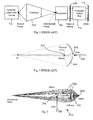
- FIG. 1 A simplified block diagram of an EUV lithography system is shown in Fig. 1 (PRIOR ART).
- the EUV source 102 at 13.5 nm is normally a hot plasma the emission of which is collected by the collector 104 and delivered to an illuminator 106 through an intermediate focus (IF).
- IF intermediate focus
- the latter illuminates a mask or reticle 108 with the pattern to be transferred to the wafer 110.
- the image of the mask or reticle is projected onto the wafer 110 by the projection optics box 112.
- the main purpose of the collector 104 is to deliver the maximum amount of in-band power from the source 102 to the illuminator 106, by matching the constraint due to the source 102 and the illuminator 106 itself.
- the ratio between the total EUV power available at the IF and the total power EUV power emitted by the source 102 in 2 ⁇ sr is called collection efficiency.
- the primary goal of the optical design of the collector 104 is to maximize the collection efficiency while matching the boundary constraints due to the source 102 and the illuminator 106.
- the EUV radiation has a wavelength of the order 13.5 nm, and for this, two types of plasma sources are currently considered as possible solutions to generate the radiation: Discharge Produced Plasma (DPP) sources and Laser Produced Plasma (LPP) sources.
- DPP Discharge Produced Plasma
- LPP Laser Produced Plasma
- the plasma is generated by means of an electric discharge through the fuel (e.g. Sn, Xe, etc.)
- the plasma is produced by a laser beam impacting on a fuel target (e.g. Li, Sn, Xe, etc.).
- Fig. 2 For an LPP source, the conventional configuration of choice is shown in Fig. 2 (PRIOR ART); see US 2005/0199829 A1 .
- a single elliptical (collector) mirror 104 is placed behind the source 102.
- the laser beam 204 reaches the fuel target at the source (focus) 102 from the side of the mirror 104 opposite to the IF, through a hole 206 in the center of the mirror 104.
- the incidence angles on the mirror 104 are normally smaller than about 30°, and a multilayer coating (normally consisting of a Mo and Si stack) is required to assure enough reflectivity at 13.5 nm.
- Mirrors with small incidence angles will be referred to herein as Normal Incidence Mirrors (NIM).
- NIM Normal Incidence Mirrors
- the configuration of Fig. 2 is the most efficient. However, this configuration has several drawbacks -
- the present invention seeks to address the aforementioned and other issues.
- a source-collector system for EUV and X-ray applications for example at 13.5 nm, comprising a grazing incidence collector in combination with a laser produced plasma (LPP) source.
- LPP laser produced plasma
- one or more further optical elements act upon one or more laser beams used to generate the EUV or X-ray plasma source, whereby said laser beam(s) impact(s) on the fuel target from a side thereof on which an intermediate focus is disposed.
- a collector for EUV and X-ray applications in which radiation from a plasma source is reflected by the collector to an intermediate focus, the line joining the source and intermediate focus defining an optical axis, a first direction on the optical axis being defined from the source to the intermediate focus, characterised by the collector comprising one or more grazing incidence mirrors; and by the collector comprising one or more further optical elements for redirecting a received laser beam so as to be incident upon the source (a) in a second direction, opposite to said first direction, or (b) at an acute angle to said second direction.
- said one or more further optical elements comprise a plane mirror disposed between the collector and the intermediate focus, for reflecting said received laser beam that is propagating in a direction non-parallel to the optical axis.
- the plane mirror is disposed on the optical axis.
- the plane mirror is disposed in a plane at 45 degrees to the optical axis, for reflecting said received laser beam that is propagating in a direction transverse to the optical axis.
- said one or more further optical elements comprise a spherical mirror disposed between the source and the intermediate focus, for reflecting said received laser beam that is propagating in a said first direction from a side of the source opposite the collector.
- the spherical mirror is disposed between the source and the collector, or is disposed at the end of the collector nearest to the source.
- said one or more further optical elements comprise; a convex lens disposed a side of the source opposite the collector, for focussing said received laser beam that is propagating in a said first direction from a side of the source opposite the collector, and a plane mirror disposed between the source and the intermediate focus, for reflecting said laser beam so that it propagates in said second direction towards the source.
- said one or more further optical elements comprise: a plane mirror disposed on the optical axis between the collector and the intermediate focus, for reflecting said received laser beam that is propagating in a direction transverse to the optical axis, the plane mirror being disposed in a plane at 45 degrees to the optical axis, and a convex lens, disposed between the plane mirror and the source, for focussing the laser beam onto the source.
- an EUV lithography system comprising: a radiation source, for example a LPP source; the collector optical system of any of claims 4 to 11 of the appended claims; an optical condenser; and a reflective mask.
- a collector for application at about 13.5 nm with Laser Produced Plasma sources comprising between 5 and 16 concentrically aligned mirrors, and preferably between 6 and 12 mirrors, that operate at grazing incidence such that the maximum grazing angle between the incident radiation and the reflective surface of the mirrors is about 30°, and more preferably about 25°, in order to allow a maximum collection angle from the source of about 40° to about 85°, and preferably about 45° to about 75°.
- the or each mirror comprises a Wolter mirror. In one embodiment, the or each mirror comprises an elliptical mirror. In one embodiment, the or each mirror comprises an "equal reflection angle” mirror. In one embodiment, the or each mirror comprises an "off-axis Wolter” mirror.
- the collector comprises a plurality of concentrically aligned mirrors of different designs, the designs including Wolter, elliptical, "equal reflection angle,” “off-axis Wolter” designs.
- a collector for application at about 13.5 nm with Laser Produced Plasma sources comprising a plurality of concentrically aligned mirrors wherein the mirrors are made from metal, preferably Ni, Cu, or Al, and are formed by diamond turning such that the mirror thickness is between about 0.5 mm and about 4 mm and preferably between about 1 mm and about 3 mm.
- a collector for application at about 13.5 nm with Laser Produced Plasma sources comprising a plurality of concentrically aligned mirrors, wherein the mirrors are made by metal electroforming, preferably Ni or Cu, such that the mirror thickness is between about 0.5 mm and about 4 mm and more preferably between about 1 mm and about 3 mm.
- a collector for application at about 13.5 nm with Laser Produced Plasma sources comprising a plurality of concentrically aligned mirrors, wherein the mirrors are made of a multilayer of electroformed metals, the multilayer comprising a thin layer of Ni, preferably with a thickness of about 0.01 mm to about 0.3 mm, followed by a thick layer of Cu, preferably with a thickness between about 0.5 mm and about 4 mm, followed by a thin layer of Ni, preferably with a thickness of about 0.01 mm to about 0.3 mm.
- a collector for application at about 13.5 nm with Laser Produced Plasma sources comprising a plurality of concentrically aligned mirrors, wherein the mirrors are made by a multilayer of electroformed metals consisting of a thin layer of NiCo alloy, preferably with a thickness of about 0.01 mm to 0.3 mm, followed by a thick layer of Cu, preferably with a thickness between 0.5 mm and 4 mm, followed by a thin layer of NiCo alloy, preferably with a thickness of about 0.01 mm to 0.3 mm.
- the electroformed mirrors have a surface roughness preferably below 2 nm in the spatial wavelength range between 1 mm and 10 nm more preferably, below 1 nm in the spatial wavelength range between 1 mm and 10 nm.
- a collector for application at about 13.5 nm with Laser Produced Plasma sources consisting of a plurality of concentrically aligned mirrors wherein the mirrors are produced by an electroforming process in which the separation layer comprises a material different from Au, or in which Au is confined between the mirror substrate and the reflective coating by using a suitable barrier material so that substantially no Au can escape.
- a collector for application at about 13.5 nm with Laser Produced Plasma sources comprising a plurality of concentrically aligned mirrors wherein the mirrors have a surface roughness preferably below 2 nm in the spatial wavelength range between 1 mm and 10 nm and, more preferably, below 1 nm in the spatial wavelength range between 1 mm and 10 nm.
- a collector for application at 13.5 nm or thereabouts with Laser Produced Plasma sources comprising a plurality of concentrically aligned mirrors and an integrated thermal management, wherein the integrated thermal management system maintains, in use, the temperature of the mirrors and the supporting structure substantially constant in time, preferably within ⁇ 5 °C and more preferably within ⁇ 2 °C and even more preferably within ⁇ 1 °C with respect to a desired temperature, and/or substantially uniform over the mirror surface, preferably within ⁇ 5 °C and more preferably within ⁇ 2 °C and even more preferably within ⁇ 1 °C with respect to a desired temperature.
- the integrated thermal management includes a control feedback loop and control software.
- the integrated thermal management includes cooling and heating elements mounted on one or more of the mirrors thereon, for example on the rear side thereof.
- the cooling and heating elements comprises pipelines cooled by fluids or phase-transition fluids, Peltier cells, micro-channels obtained by micro-machining the rear surface of the mirrors or by proper masking the rear surface of the mirror during the electroforming process, pipelines heated by a suitable fluid or wires heated by Joule effect.
- a collector for application at about 13.5 nm with Laser Produced Plasma sources comprising a plurality of concentrically aligned mirrors, wherein a shield in the form of a thin circular annulus with the same dimensions of the mirror edge is disposed in front of an entrance edge of one or more mirrors and attached thereto by a mechanical coupling with negligible or limited thermal contact with the mirror, such that the shield completely or partially prevents the radiation from the source or from the debris mitigation tool irradiating the mirror edge.
- a collector for application at about 13.5 nm with Laser Produced Plasma sources comprising a plurality of concentrically aligned mirrors, wherein a cooled pipeline is attached in front of an entrance edge of one or more mirrors.
- a collector for application at about 13.5 nm or thereabouts with Laser Produced Plasma sources, the collector comprising a plurality of concentrically aligned mirrors, wherein the optical surfaces are coated by a reflective layer, the reflective layer preferably being made of (a) one of Pd, Au, Ir, Pt, Mo, Rh, and more preferably Ru, or (b) a nano-composite alloy of two or more of Pd, Au, Ir, Pt, Mo, Rh, and Ru, with the reflective layer having a thickness between about 50 nm and about 500 nm; and the reflective layer along the length of the collector being for example of uniform in thickness.
- a collector for application at about 13.5 nm with Laser Produced Plasma sources comprising a plurality of concentrically aligned mirrors, wherein optical surfaces of the mirrors are coated by a reflective layer made of (a) one of Pd, Au, Ir, Pt, Mo, Rh, and Ru, or (b) a nano-composite alloy of two or more of Pd, Au, Ir, Pt, Mo, Rh, and Ru, with the reflective layer having a thickness between about 500 nm and about 3000 nm in order to extend the collector lifetime against erosion from debris from the source; and the reflective layer along the length of the collector being for example of uniform in thickness.
- a collector for application at about 13.5 nm with Laser Produced Plasma sources and debris mitigation tools, the collector comprising a plurality of concentrically aligned mirrors, wherein the geometry of the collector matches the geometry of the debris mitigation tools.
- a collector for application at about 13.5 nm with Laser Produced Plasma sources and debris mitigation tools comprising a plurality of concentrically aligned mirrors and a support structure, wherein the support structure of the collector and the debris mitigation tools have matched dimensions and are aligned to avoid additional obscuration and to maximize the combined collection efficiency of the debris mitigation tool and the collector.
- a collector for application at about 13.5 nm with Laser Produced Plasma sources comprising a plurality of concentrically aligned mirrors, wherein one or more of the mirrors has mounted thereon, for example on the rear side thereof, one or more devices for the mitigation of debris from the source, for example erosion detectors, solenoids and RF sources.
- a collector for application at about 13.5 nm with Laser Produced Plasma sources comprising a plurality of concentrically aligned mirrors and a support structure, wherein the collector is made of non-ferromagnetic materials.
- a collector for application at about 13.5 nm with Laser Produced Plasma sources comprising a plurality of concentrically aligned mirrors, wherein non-reflective surfaces of the mirrors are coated by a protective layer of Rh and preferably with a thickness between about 50 nm and about 3000 nm, and preferably deposited by galvanic plating.
- the mirrors consist of electroformed Cu preferably with a thickness between about 0.5 mm and about 4 mm, a reflective layer, preferably of thickness between 50 mm and 3000 nm and more preferably between about 500 and about 3000 nm, on an optical surface of the electroformed Cu, wherein the reflective layer thickness along the length of the collector is for example uniform.
- a method of manufacturing the collector of any of claims 20 to 22, comprising: preparing masters; electroforming the mirrors on the masters; wherein the masters are manufactured by diamond turning and polished such that the masters have a surface roughness in the spatial wavelength range between 1 mm and 10 nm of below 2 nm, and preferably below 1 nm.
- a method of manufacturing masters comprising diamond turning and polishing a substrate to form the master, such that the masters have a surface roughness in the spatial wavelength range between 1 mm and 10 nm of below 2 nm, and preferably of below 1 nm.
- a plurality of concentrically aligned two-reflection mirrors is used for the collector, for example a type I Wolter collector.
- the incidence angles on the mirror(s) of the collector are normally larger than c. 60° (i.e. grazing angle ⁇ c. 30°) and a single layer coating on the mirror surface (using for example Ru, Pd, etc.) is enough to assure large transmission at 13.5 nm.
- Mirrors with large incidence angles will be referred to herein as Grazing Incidence Mirrors (GIM).
- An advantage of the invention is that the GIM (e.g. Fig. 3 ) only needs a reflective monolayer coating of Ru, Pd, etc., rather than a multilayer.
- a further advantage of the invention is that the surface area of the GIM is much larger than the one of the NIM and consequently the thermal load density is much lower in the former case, facilitating thermal control.
- a further advantage is that the use of a monolayer with the GIM omits narrow pass-band filter effects of the multilayer, so that the total thermal load is lower on a GIM than on a NIM.
- a further advantage of the invention is that the use of Debris Mitigation Tools (DMT) commonly used with DPP sources is also enabled.
- DMT Debris Mitigation Tools
- a further advantage is that there is reduced or no need to increase the thickness of the reflective layer by increasing the numbers of layers in the multilayer coating, to overcome the erosion of the reflective layer by high energy ions and particles from the source and extend the lifetime of the mirror.
- a GIM only the thickness of the single reflective coating needs to be increased.
- a further advantage is that the ion and particle flow (per unit area) is lower in a GIM than in a NIM, due to the larger area of the GIM. Consequently, at equal ion and particle flow rate, the erosion and/or deposition is lower in a GIM than in a NIM.
- references to an "image focus” are references to an image focus or to an intermediate focus.
- FIG. 3 shows a grazing incidence collector 302 according to a first embodiment of the invention, for use with a LPP source 304.
- the collector 302 consists of a plurality of concentrically aligned mirrors or shells 306; in this embodiment, there are six mirrors 306, as shown in Fig. 3 ; however, it will be appreciated that any suitable number of mirrors may be used.
- Each mirror 306 may have the same or different design, including, but not limited to, Wolter, elliptical, "equal reflection angle," and "off-axis Wolter” designs.
- the design of such "equal reflection angle" grazing incidence collectors is discussed in, for example, European patent application no. 06425539.1 (attorney's ref.
- the laser beam 308 propagates from the same side of the collector 302 as the IF, through a flat folding mirror 310. After reflection at the mirror 310, the laser beam 308 propagates (in the direction of arrow A) towards the source (fuel) 304 (e.g. Li, Sn, Xe, etc.).
- the angular emission of LPP sources 304 may be anisotropic, with the peak emission in the direction opposite to the laser beam propagation.
- An example of the angular distribution of the radiated EUV power is shown in Fig. 4 .
- the maximum intensity of the radiation being emitted is toward the collector 302 (i.e. opposite to arrow A).
- the thickness of the mirror(s) 306 has a direct impact on the collection efficiency, as part of the EUV radiation emitted from the source 304 is blocked by the mirror thickness.
- the thickness of the mirror(s) 306 must be kept as small as possible. Therefore, metal is suitably used for the manufacturing of the mirrors 306: this allows a small mirror thickness and provides enough mechanical and structural stiffness to avoid the mirror deforming under its own weight.
- the fraction of EUV radiation emitted from the plasma source is only a small fraction of the total power radiated by the source, a large amount of power, in the order of several kilowatts, hits the reflecting surface of the collector mirrors. Part of this power is absorbed by the collector and must be removed by a properly designed cooling system to avoid excessive deformation of the mirror.
- the use of a metal for the manufacturing of the mirror provides a large enough thermal conductance to allow the thermal power absorbed by the mirrors to flow to the cooling system.
- the mirror thickness must be properly chosen as a trade off between the need to limit the obscuration of the radiation from the source and the need to increase the thermal conductance as much as possible.
- the thickness is between about 0.5 mm and about 4 mm.
- the choice of metal for the mirror(s) 306 is a trade off between the need to ensure the mirror 306 is stiff enough and the need to increase the thermal conductance as much as possible.
- materials suitable for mirror manufacturing are Ni, Al, Cu.
- the mirrors for EUV and X-ray applications need high accuracy and very low roughness (preferably below 1-2 nm rms), the mirrors are suitably manufactured by Diamond Turning, which is known to persons skilled in the art.
- the metal mirrors may be manufactured by electroforming from a negative master (not shown), using techniques known to persons skilled in the art (see, for example W00184747 ). Fabrication by electroforming allows:
- the electroforming process replicates the shape of the master, the latter must have a surface accuracy good enough to assure acceptable optical performance of the final mirrors.
- the masters can be manufactured by diamond turning.
- Electroformed mirrors may be manufactured in a variety of metals including Ni and Ni-Co alloys. Electroformed mirrors can also be manufactured in Cu, which enables a larger thermal conductance. In the latter case, since copper may cause contamination and its use may not be allowed in the operating environment, the electroformed mirrors can be manufactured in a multilayer structure consisting of a thin layer of Ni, preferably with a thickness in the range about 0.01mm to about 0.3mm, followed by a thick layer of Cu, preferably with a thickness between 0.5 mm and 4 mm, followed by a thin layer of Ni, preferably with a thickness in the range about 0.01mm to about 0.3mm.
- the electroformed mirrors can be manufactured in a multilayer structure consisting of a thin layer of Ni-Co alloy, preferably with a thickness in the range about 0.01mm to about 0.3mm, followed by a thick layer of Cu, preferably with a thickness between 0.5 mm and 4 mm, followed by a thin layer of Ni-Co alloy, preferably with a thickness in the range about 0.01mm to about 0.3mm.
- a suitable separation layer is deposited onto the master to allow the release of the mirror from the master at the end of the electroforming process.
- a typical material used as a separation layer is Au (gold), which sticks on the whole optical surface of the mirror after the release. As Au may contaminate the operating environment it may not be allowed in such environments. In this case, two solutions can be used:
- the collector 302 may be equipped with an integrated thermal management system (not shown) to keep the temperature of the shells (mirrors 306) substantially constant and uniform, and to avoid excessive deformation induced by the large thermal load from the plasma source 304.
- the thermal management system (not shown) is integrated on the rear surface of the mirrors 306 in a region where it does not block the optical path of the radiation from the source 304.
- the integrated thermal management system may include cooling elements such as (a) pipes cooled by a suitable fluid, (b) Peltier cells, (c) pipes cooled by phase-transition fluids, (d) micro-channels obtained by micro-machining the rear surface of the mirrors or by suitable masking the rear surface of the mirror during the electroforming process.
- the integrated thermal management system (not shown) may alternatively or additionally include heating elements such as pipes heated by a suitable fluid or wires heated by Joule effect.
- the integrated thermal management system may alternatively or additionally include temperature sensors and thermal control hardware and software.
- All the above elements may be integrated in the thermal management system (not shown) that includes a feedback control loop.
- the temperature profiles of the mirrors 306 and any supporting structures are monitored in real time and used as feedback signals to activate the cooling elements (not shown) and the heating elements (not shown) and keep the temperature of the mirrors 306 and the supporting structure constant in time and uniform on the mirror surface.
- control involves a deviation from a desired temperature within ⁇ 5 °C and more preferably within ⁇ 2 °C and even more preferably within ⁇ 1 °C.
- the support structure (not shown) of the collector 302, to which the mirror shells 306 are attached, optionally are also cooled, for example to reduce or eliminate the effects of the thermal load due to thermal radiation from surrounding bodies (not shown), due to spurious plasma in the vacuum chamber (not shown), etc.
- the reflective coating (not shown) of the collector mirrors 306 is preferably protected by using a suitable debris mitigation tool (DMT) (not shown) and cleaning techniques.
- DMT debris mitigation tool
- the collector 302 must then be compatible with the DMT (not shown) in terms of dimensions, positions of supporting structures (not shown), to limit obscurations, etc.
- the collector 302 itself may optionally be equipped with debris mitigation or protective systems (not shown), for example erosion detectors, solenoids and RF sources, protective layers.
- the collector is preferably also designed to be compatible with the cleaning environment needed to remove deposition of non-reflective materials onto the optical (mirror) surface.
- a protective layer preferably Rh with a thickness between 50 nm and 3000 nm, so as to be chemically resistant to the cleaning environment.
- a protective layer preferably Rh with a thickness between 50 nm and 3000 nm, so as to be chemically resistant to the cleaning environment.
- One convenient method of depositing the protective coating material is by galvanic plating, since it allows the coating of complex surfaces such as the rear surfaces of the mirrors 306 and the supporting structure (not shown).
- the thickness of the reflective coating is suitably between about 50 nm and about 500 nm.
- the reflective coating may be eroded.
- a reflective coating (not shown) of greater thickness is preferably used, preferably up to a thickness between 500 nm and 3000 nm or more. The thickness of the reflective coating along the length of the collector may be but need not be uniform.
- the collector 302 is surrounded by an electromagnet (not shown) for producing a strong magnetic field (of the order of 1 T or more).
- This field may be strong enough to cause deformation of the collector 302 if it contains ferromagnetic materials, such as Ni or Ni-Co alloys.
- ferromagnetic materials such as Ni or Ni-Co alloys.
- non-ferromagnetic material must then be used to fabricate the collector 302.
- the collector 302 may be manufactured in electroformed Cu and be protected by a thick reflective coating (e.g. Ru; not shown) on the optical surface and by a thick protective galvanic coating (e.g. Rh; not shown) on the non-optical surfaces.
- the maximum exit numerical aperture (NA) of the collector 302 is normally limited by the entrance NA of the illuminator 106. This restriction, together with practical limits in the distance between the source 304 and the IF, also sets a limit to the length of the mirrors 306. Due to this limitation, each mirror 306 may collect only an angular fraction of the radiation from the source 304. In order to maximize the collection efficiency, the largest angle captured by the collector 302 from the source 204 must also be maximized. Consequently, a plurality of mirrors 306 must be concentrically aligned to cover the desired angular range from the source 304, typically such that the maximum collected angles lies between about 40° and about 85°. According to the first embodiment of the invention ( Fig. 3 ), six concentric mirrors 306 are employed; however, in preferred embodiments, the number of concentric mirrors 306 in a collector 302 is between 5 and 16.
- the optical surface of the mirrors 306 is coated by a suitable material, here referred as "the reflective layer”, preferably made (but not limited to) of Pd, Ir, Pt, Mo, Rh, and more preferably Ru.
- the reflective layer preferably made (but not limited to) of Pd, Ir, Pt, Mo, Rh, and more preferably Ru.
- nano-structured layers composed by one or more EUV elements from the above list, with the structure of a multilayer with nanometer periodicity or nano-composite obtained by (co)deposition of one or more EUV reflective elements with alternating structure and growth parameters can be used.
- These materials include multilayers of two elements (such as, for example, Mo, Ru, Zr, Nb Pd) with different nanostructure and interfaces (e.g. amorphous/amorphous, nanocrystalline/amorphous, etc.).
- a reactive gas such as H 2 , O 2 and N 2
- a reactive gas such as H 2 , O 2 and N 2
- the entire reflective layer so obtained is stress compensated (i.e. almost stress free or with a final residual stress adequate to obtain a mechanically stable optical layer with the substrate), with overall maximum thickness of about several micrometers (e.g. about 3-5 micrometers).
- the preferred method of deposition for these structured layers is physical, using plasma and ion assistance (sputtering, reactive sputtering, evaporation etc.) but it is not limited to these preparation methods.
- the materials of the reflective layer may be already nano-alloyed as the result of the deposition process, or may be post-treated to reach the final nano-structure.
- One variant of the above reflective layer composition is as follows: rather than a plurality, a single element (such as, for example, Mo, Ru, Zr, Nb or Pd) with modulated electronic and physical properties, obtained by ion bombardment during growth to change the film density and intrinsic residual stress, is formed.
- This stress-compensated nano-structured EUV layer exhibits high EUV reflectivity and can be grown to a maximum of several micrometers (e.g. about 3-5 micrometers).
- the angle between the incoming radiation and the reflecting surface of the mirrors 306 must be kept below a certain limit, beyond which the reflectivity of the reflective coating drops to small values, thus decreasing the collection efficiency.
- this grazing angle is between about 20-30°.
- the optical design of the collector mirror is preferably such that the grazing angle is below 30°.
- Figure 5 shows a grazing incidence collector according to a second embodiment of the invention. This is the same as the first embodiment, except as follows.
- the laser beam 308 propagates initially from the side of the collector 302' opposite the IF (i.e. in the direction of arrow B) and is reflected back and focused onto the fuel target (corresponding to source focus 304, and produced by fuel droplet generator 313) by means of a spherical mirror 314.
- the mirror 314 may be a cooled mirror.
- An exemplary consequent emitted/reflected EUV ray is indicated by 316.
- FIG. 6 shows a grazing incidence collector according to a third embodiment of the invention. This is the same as the first embodiment, except as follows.
- laser beam 308 propagates initially from the side of the collector 302" opposite the IF. It is focused by a large diameter lens 318, which therefore is subjected to lower laser pulse energy density.
- the beam 308 is then reflected back onto the fuel target fuel target (corresponding to source focus 304, and produced by fuel droplet generator 313) by means of a flat mirror 320.
- the mirror 320 may be a cooled mirror.
- An exemplary consequent emitted/reflected EUV ray is indicated by 316.
- FIG. 7 illustrates a grazing incidence collector according to a fourth embodiment of the invention.
- the laser beam 308 propagates perpendicularly to the optical axis 322 of the collector 302"'.
- the beam 308 is then folded by 90° by means of a flat mirror 324 (located on the optical axis on the same side of the collector 302"' as the IF) and is focused onto the fuel target (corresponding to source focus 304, and produced by fuel droplet generator 313) by means of a lens 326.
- a rather large volume 328 is available for generating fuel droplets, for the hardware (not shown) needed to generate magnetic fields, etc.
- Figure 8 shows a grazing incidence collector according to a fifth embodiment of the invention. This is the same as the first embodiment, except as follows. Again, laser beam 308 propagates initially from the side of the collector 302"" opposite the IF. However, in this case the laser beam is incident directly on the source. When the source angular emission is anisotropic ( Fig. 4 ), the configuration of Fig. 8 , which is the extension of Fig. 2 and in which the laser beam is propagating from the side of the collector 302"" opposite the IF, is substantially less efficient because the maximum of the emission from the source takes place in the direction opposite to the collector.
- more than one laser beam may be used to generate the EUV plasma. It will also be appreciated that the laser beam, upon impact with the fuel target (at the source focus), need not be propagating along the optical axis, but at an angle thereto.
- collector optics for imaging e.g. EUV or X-ray
- EUV lithography systems Fig. 1
- imaging systems incorporating such optics the design of such imaging optics and imaging systems is discussed in, for example, European patent application no. 06425539.1 (attorney's ref. ML00H19/P-EP).
Abstract
Description
- The present invention relates to collector optical systems for EUV and X-ray applications, and more particularly to grazing incidence collector optics for laser produced plasma (LPP) sources.
- The invention has various applications in scenarios where EUV and X-ray radiation is used, but is particularly useful in lithography and imaging applications.
- A simplified block diagram of an EUV lithography system is shown in
Fig. 1 (PRIOR ART). TheEUV source 102 at 13.5 nm is normally a hot plasma the emission of which is collected by thecollector 104 and delivered to anilluminator 106 through an intermediate focus (IF). The latter illuminates a mask orreticle 108 with the pattern to be transferred to thewafer 110. The image of the mask or reticle is projected onto thewafer 110 by theprojection optics box 112. The main purpose of thecollector 104 is to deliver the maximum amount of in-band power from thesource 102 to theilluminator 106, by matching the constraint due to thesource 102 and theilluminator 106 itself. The ratio between the total EUV power available at the IF and the total power EUV power emitted by thesource 102 in 2π sr is called collection efficiency. The primary goal of the optical design of thecollector 104 is to maximize the collection efficiency while matching the boundary constraints due to thesource 102 and theilluminator 106. - For preferred applications, the EUV radiation has a wavelength of the order 13.5 nm, and for this, two types of plasma sources are currently considered as possible solutions to generate the radiation: Discharge Produced Plasma (DPP) sources and Laser Produced Plasma (LPP) sources. In the former case, the plasma is generated by means of an electric discharge through the fuel (e.g. Sn, Xe, etc.), whereas in the latter case, the plasma is produced by a laser beam impacting on a fuel target (e.g. Li, Sn, Xe, etc.).
- For an LPP source, the conventional configuration of choice is shown in
Fig. 2 (PRIOR ART); seeUS 2005/0199829 A1 . A single elliptical (collector)mirror 104 is placed behind thesource 102. In the standard configuration, the laser beam 204 reaches the fuel target at the source (focus) 102 from the side of themirror 104 opposite to the IF, through ahole 206 in the center of themirror 104. The incidence angles on themirror 104 are normally smaller than about 30°, and a multilayer coating (normally consisting of a Mo and Si stack) is required to assure enough reflectivity at 13.5 nm. Mirrors with small incidence angles will be referred to herein as Normal Incidence Mirrors (NIM). The configuration ofFig. 2 is the most efficient. However, this configuration has several drawbacks - - 1) The elliptical NIM of
Fig. 2 requires a complex and expensive Mo / Si multilayer coating. - 2) The surface area of the NIM is relatively small and consequently the thermal load density is very high. This makes the thermal control of the NIM challenging.
- 3) Since plasma sources emit most of their power between about 10 nm and 120 nm, and since the multilayer coating acts as a very narrow pass-band filter reflecting only a very small bandwidth around 13.5 nm, the total thermal load is higher on the NIM. This further complicates the thermal control of a NIM.
- 4) The configuration of
Fig. 2 prevents the use of Debris Mitigation Tools (DMT) commonly used with DPP sources. This type of DMT consists of many thin lamellas radially placed around the source and filled with a gas (e.g. Ar, N2, etc.) to slow down fast particles from the source. However, this type of DMT would completely block the radiation in the configuration ofFig. 2 . - 5) To overcome the erosion of the reflective layer by high-energy ions and particles from the source and to extend the lifetime of the mirror, the thickness of the reflective layer needs to be increased. However, in a NIM this implies increasing the numbers of layers in the multilayer coating, also increasing the complexity and costs of the manufacturing process.
- 6) The ion and particle flow (per unit area) is relatively high in a NIM, due to its small area. Consequently, the erosion and/or deposition is relatively high in a NIM.
- The present invention seeks to address the aforementioned and other issues.
- According to one aspect of the present invention there is provided a source-collector system for EUV and X-ray applications, for example at 13.5 nm, comprising a grazing incidence collector in combination with a laser produced plasma (LPP) source.
- Preferably, one or more further optical elements act upon one or more laser beams used to generate the EUV or X-ray plasma source, whereby said laser beam(s) impact(s) on the fuel target from a side thereof on which an intermediate focus is disposed.
- According to another aspect of the present invention there is provided the use in EUV and X-ray applications, for example at 13.5 nm, of a grazing incidence collector in combination with a laser produced plasma (LPP) source.
- According to another aspect of the present invention there is provided a collector for EUV and X-ray applications, in which radiation from a plasma source is reflected by the collector to an intermediate focus, the line joining the source and intermediate focus defining an optical axis, a first direction on the optical axis being defined from the source to the intermediate focus, characterised by the collector comprising one or more grazing incidence mirrors; and by the collector comprising one or more further optical elements for redirecting a received laser beam so as to be incident upon the source (a) in a second direction, opposite to said first direction, or (b) at an acute angle to said second direction.
- In one embodiment, said one or more further optical elements comprise a plane mirror disposed between the collector and the intermediate focus, for reflecting said received laser beam that is propagating in a direction non-parallel to the optical axis. Preferably, the plane mirror is disposed on the optical axis. Preferably, the plane mirror is disposed in a plane at 45 degrees to the optical axis, for reflecting said received laser beam that is propagating in a direction transverse to the optical axis.
- In another embodiment, said one or more further optical elements comprise a spherical mirror disposed between the source and the intermediate focus, for reflecting said received laser beam that is propagating in a said first direction from a side of the source opposite the collector. Preferably, the spherical mirror is disposed between the source and the collector, or is disposed at the end of the collector nearest to the source.
- In another embodiment, said one or more further optical elements comprise; a convex lens disposed a side of the source opposite the collector, for focussing said received laser beam that is propagating in a said first direction from a side of the source opposite the collector, and a plane mirror disposed between the source and the intermediate focus, for reflecting said laser beam so that it propagates in said second direction towards the source.
- In another embodiment, said one or more further optical elements comprise: a plane mirror disposed on the optical axis between the collector and the intermediate focus, for reflecting said received laser beam that is propagating in a direction transverse to the optical axis, the plane mirror being disposed in a plane at 45 degrees to the optical axis, and a convex lens, disposed between the plane mirror and the source, for focussing the laser beam onto the source.
- According to another aspect of the present invention there is provided an EUV lithography system comprising: a radiation source, for example a LPP source; the collector optical system of any of claims 4 to 11 of the appended claims; an optical condenser; and a reflective mask.
- According to another aspect of the present invention there is provided a collector for application at about 13.5 nm with Laser Produced Plasma sources, the collector comprising between 5 and 16 concentrically aligned mirrors, and preferably between 6 and 12 mirrors, that operate at grazing incidence such that the maximum grazing angle between the incident radiation and the reflective surface of the mirrors is about 30°, and more preferably about 25°, in order to allow a maximum collection angle from the source of about 40° to about 85°, and preferably about 45° to about 75°.
- In one embodiment, the or each mirror comprises a Wolter mirror. In one embodiment, the or each mirror comprises an elliptical mirror. In one embodiment, the or each mirror comprises an "equal reflection angle" mirror. In one embodiment, the or each mirror comprises an "off-axis Wolter" mirror.
- In one embodiment, the collector comprises a plurality of concentrically aligned mirrors of different designs, the designs including Wolter, elliptical, "equal reflection angle," "off-axis Wolter" designs.
- According to another aspect of the present invention there is provided a collector for application at about 13.5 nm with Laser Produced Plasma sources, the collector comprising a plurality of concentrically aligned mirrors wherein the mirrors are made from metal, preferably Ni, Cu, or Al, and are formed by diamond turning such that the mirror thickness is between about 0.5 mm and about 4 mm and preferably between about 1 mm and about 3 mm.
- According to another aspect of the present invention there is provided a collector for application at about 13.5 nm with Laser Produced Plasma sources, the collector comprising a plurality of concentrically aligned mirrors, wherein the mirrors are made by metal electroforming, preferably Ni or Cu, such that the mirror thickness is between about 0.5 mm and about 4 mm and more preferably between about 1 mm and about 3 mm.
- According to another aspect of the present invention there is provided a collector for application at about 13.5 nm with Laser Produced Plasma sources, the collector comprising a plurality of concentrically aligned mirrors, wherein the mirrors are made of a multilayer of electroformed metals, the multilayer comprising a thin layer of Ni, preferably with a thickness of about 0.01 mm to about 0.3 mm, followed by a thick layer of Cu, preferably with a thickness between about 0.5 mm and about 4 mm, followed by a thin layer of Ni, preferably with a thickness of about 0.01 mm to about 0.3 mm.
- According to another aspect of the present invention there is provided a collector for application at about 13.5 nm with Laser Produced Plasma sources, the collector comprising a plurality of concentrically aligned mirrors, wherein the mirrors are made by a multilayer of electroformed metals consisting of a thin layer of NiCo alloy, preferably with a thickness of about 0.01 mm to 0.3 mm, followed by a thick layer of Cu, preferably with a thickness between 0.5 mm and 4 mm, followed by a thin layer of NiCo alloy, preferably with a thickness of about 0.01 mm to 0.3 mm.
- Preferably, the electroformed mirrors have a surface roughness preferably below 2 nm in the spatial wavelength range between 1 mm and 10 nm more preferably, below 1 nm in the spatial wavelength range between 1 mm and 10 nm.
- According to another aspect of the present invention there is provided a collector for application at about 13.5 nm with Laser Produced Plasma sources, the collector consisting of a plurality of concentrically aligned mirrors wherein the mirrors are produced by an electroforming process in which the separation layer comprises a material different from Au, or in which Au is confined between the mirror substrate and the reflective coating by using a suitable barrier material so that substantially no Au can escape.
- According to another aspect of the present invention there is provided a collector for application at about 13.5 nm with Laser Produced Plasma sources, the collector comprising a plurality of concentrically aligned mirrors wherein the mirrors have a surface roughness preferably below 2 nm in the spatial wavelength range between 1 mm and 10 nm and, more preferably, below 1 nm in the spatial wavelength range between 1 mm and 10 nm.
- According to another aspect of the present invention there is provided a collector for application at 13.5 nm or thereabouts with Laser Produced Plasma sources, the collector comprising a plurality of concentrically aligned mirrors and an integrated thermal management, wherein the integrated thermal management system maintains, in use, the temperature of the mirrors and the supporting structure substantially constant in time, preferably within ±5 °C and more preferably within ±2 °C and even more preferably within ±1 °C with respect to a desired temperature, and/or substantially uniform over the mirror surface, preferably within ±5 °C and more preferably within ±2 °C and even more preferably within ±1 °C with respect to a desired temperature.
- Preferably, the integrated thermal management includes a control feedback loop and control software.
- Alternatively or additionally, the integrated thermal management includes cooling and heating elements mounted on one or more of the mirrors thereon, for example on the rear side thereof. Preferably, the cooling and heating elements comprises pipelines cooled by fluids or phase-transition fluids, Peltier cells, micro-channels obtained by micro-machining the rear surface of the mirrors or by proper masking the rear surface of the mirror during the electroforming process, pipelines heated by a suitable fluid or wires heated by Joule effect.
- According to another aspect of the present invention there is provided a collector for application at about 13.5 nm with Laser Produced Plasma sources, the collector comprising a plurality of concentrically aligned mirrors, wherein a shield in the form of a thin circular annulus with the same dimensions of the mirror edge is disposed in front of an entrance edge of one or more mirrors and attached thereto by a mechanical coupling with negligible or limited thermal contact with the mirror, such that the shield completely or partially prevents the radiation from the source or from the debris mitigation tool irradiating the mirror edge.
- According to another aspect of the present invention there is provided a collector for application at about 13.5 nm with Laser Produced Plasma sources, the collector comprising a plurality of concentrically aligned mirrors, wherein a cooled pipeline is attached in front of an entrance edge of one or more mirrors.
- According to another aspect of the present invention there is provided a collector for application at about 13.5 nm or thereabouts with Laser Produced Plasma sources, the collector comprising a plurality of concentrically aligned mirrors, wherein the optical surfaces are coated by a reflective layer, the reflective layer preferably being made of (a) one of Pd, Au, Ir, Pt, Mo, Rh, and more preferably Ru, or (b) a nano-composite alloy of two or more of Pd, Au, Ir, Pt, Mo, Rh, and Ru, with the reflective layer having a thickness between about 50 nm and about 500 nm; and the reflective layer along the length of the collector being for example of uniform in thickness.
- According to another aspect of the present invention there is provided a collector for application at about 13.5 nm with Laser Produced Plasma sources, the collector comprising a plurality of concentrically aligned mirrors, wherein optical surfaces of the mirrors are coated by a reflective layer made of (a) one of Pd, Au, Ir, Pt, Mo, Rh, and Ru, or (b) a nano-composite alloy of two or more of Pd, Au, Ir, Pt, Mo, Rh, and Ru, with the reflective layer having a thickness between about 500 nm and about 3000 nm in order to extend the collector lifetime against erosion from debris from the source; and the reflective layer along the length of the collector being for example of uniform in thickness.
- According to another aspect of the present invention there is provided a collector for application at about 13.5 nm with Laser Produced Plasma sources and debris mitigation tools, the collector comprising a plurality of concentrically aligned mirrors, wherein the geometry of the collector matches the geometry of the debris mitigation tools.
- According to another aspect of the present invention there is provided a collector for application at about 13.5 nm with Laser Produced Plasma sources and debris mitigation tools, the collector comprising a plurality of concentrically aligned mirrors and a support structure, wherein the support structure of the collector and the debris mitigation tools have matched dimensions and are aligned to avoid additional obscuration and to maximize the combined collection efficiency of the debris mitigation tool and the collector.
- According to another aspect of the present invention there is provided a collector for application at about 13.5 nm with Laser Produced Plasma sources, the collector comprising a plurality of concentrically aligned mirrors, wherein one or more of the mirrors has mounted thereon, for example on the rear side thereof, one or more devices for the mitigation of debris from the source, for example erosion detectors, solenoids and RF sources.
- According to another aspect of the present invention there is provided a collector for application at about 13.5 nm with Laser Produced Plasma sources, the collector comprising a plurality of concentrically aligned mirrors and a support structure, wherein the collector is made of non-ferromagnetic materials.
- According to another aspect of the present invention there is provided a collector for application at about 13.5 nm with Laser Produced Plasma sources, the collector comprising a plurality of concentrically aligned mirrors, wherein non-reflective surfaces of the mirrors are coated by a protective layer of Rh and preferably with a thickness between about 50 nm and about 3000 nm, and preferably deposited by galvanic plating.
- Preferably, the mirrors consist of electroformed Cu preferably with a thickness between about 0.5 mm and about 4 mm, a reflective layer, preferably of thickness between 50 mm and 3000 nm and more preferably between about 500 and about 3000 nm, on an optical surface of the electroformed Cu, wherein the reflective layer thickness along the length of the collector is for example uniform.
- According to another aspect of the present invention there is provided a method of manufacturing the collector of any of
claims 20 to 22, comprising: preparing masters; electroforming the mirrors on the masters; wherein the masters are manufactured by diamond turning and polished such that the masters have a surface roughness in the spatial wavelength range between 1 mm and 10 nm of below 2 nm, and preferably below 1 nm. - According to another aspect of the present invention there is provided a method of manufacturing masters, the masters being for the fabrication of mirrors by electroforming, the mirrors being for use in a collector of any of
claims 20 to 22, the method comprising diamond turning and polishing a substrate to form the master, such that the masters have a surface roughness in the spatial wavelength range between 1 mm and 10 nm of below 2 nm, and preferably of below 1 nm. - In accordance with preferred embodiments of the invention, a plurality of concentrically aligned two-reflection mirrors is used for the collector, for example a type I Wolter collector. The incidence angles on the mirror(s) of the collector are normally larger than c. 60° (i.e. grazing angle < c. 30°) and a single layer coating on the mirror surface (using for example Ru, Pd, etc.) is enough to assure large transmission at 13.5 nm. Mirrors with large incidence angles will be referred to herein as Grazing Incidence Mirrors (GIM).
- An advantage of the invention is that the GIM (e.g.
Fig. 3 ) only needs a reflective monolayer coating of Ru, Pd, etc., rather than a multilayer. - A further advantage of the invention is that the surface area of the GIM is much larger than the one of the NIM and consequently the thermal load density is much lower in the former case, facilitating thermal control.
- A further advantage is that the use of a monolayer with the GIM omits narrow pass-band filter effects of the multilayer, so that the total thermal load is lower on a GIM than on a NIM.
- A further advantage of the invention is that the use of Debris Mitigation Tools (DMT) commonly used with DPP sources is also enabled.
- A further advantage is that there is reduced or no need to increase the thickness of the reflective layer by increasing the numbers of layers in the multilayer coating, to overcome the erosion of the reflective layer by high energy ions and particles from the source and extend the lifetime of the mirror. In a GIM, only the thickness of the single reflective coating needs to be increased.
- A further advantage is that the ion and particle flow (per unit area) is lower in a GIM than in a NIM, due to the larger area of the GIM. Consequently, at equal ion and particle flow rate, the erosion and/or deposition is lower in a GIM than in a NIM.
- Embodiments of the invention will now be described in detail, by way of example, with reference to the accompanying drawings, in which:
-
Figure 1 (PRIOR ART) shows an example of a known EUV lithography system; -
Figure 2 (PRIOR ART) depicts an example of the collector optics for the EUV lithography system ofFig. 1 , for use with a LPP source; -
Figure 3 shows a grazing incidence collector according to a first embodiment of the invention, for use with a LPP source; -
Figure 4 illustrates the angular distribution of the radiated EUV power for the LPP source used with the collector ofFig.3 ; -
Figure 5 shows a grazing incidence collector according to a second embodiment of the invention; -
Figure 6 shows a grazing incidence collector according to a third embodiment of the invention; -
Figure 7 illustrates a grazing incidence collector according to a fourth embodiment of the invention; and -
Figure 8 shows a grazing incidence collector according to a fifth embodiment of the invention. - In the description and drawings, like numerals are used to designate like elements. Unless indicated otherwise, any individual design features and components may be used in combination with any other design features and components disclosed herein.
- In the illustrations of optical elements or systems herein, unless indicated otherwise, cylindrical symmetry around the optical axis is assumed; and references to an "image focus" are references to an image focus or to an intermediate focus.
-
Figure 3 shows agrazing incidence collector 302 according to a first embodiment of the invention, for use with aLPP source 304. Thecollector 302 consists of a plurality of concentrically aligned mirrors orshells 306; in this embodiment, there are sixmirrors 306, as shown inFig. 3 ; however, it will be appreciated that any suitable number of mirrors may be used. Eachmirror 306 may have the same or different design, including, but not limited to, Wolter, elliptical, "equal reflection angle," and "off-axis Wolter" designs. The design of such "equal reflection angle" grazing incidence collectors is discussed in, for example, European patent application no.06425539.1 06425634.0 - In this embodiment, the
laser beam 308 propagates from the same side of thecollector 302 as the IF, through aflat folding mirror 310. After reflection at themirror 310, thelaser beam 308 propagates (in the direction of arrow A) towards the source (fuel) 304 (e.g. Li, Sn, Xe, etc.). The angular emission ofLPP sources 304 may be anisotropic, with the peak emission in the direction opposite to the laser beam propagation. An example of the angular distribution of the radiated EUV power is shown inFig. 4 . Returning toFig. 3 , in this case, if the emission from thesource 304 is anisotropic, the maximum intensity of the radiation being emitted is toward the collector 302 (i.e. opposite to arrow A). - In a concentric mirror configuration, like the Wolter design shown in
Fig. 3 , the thickness of the mirror(s) 306 has a direct impact on the collection efficiency, as part of the EUV radiation emitted from thesource 304 is blocked by the mirror thickness. To achieve the maximum possible collection efficiency, the thickness of the mirror(s) 306 must be kept as small as possible. Therefore, metal is suitably used for the manufacturing of the mirrors 306: this allows a small mirror thickness and provides enough mechanical and structural stiffness to avoid the mirror deforming under its own weight. - Since the fraction of EUV radiation emitted from the plasma source is only a small fraction of the total power radiated by the source, a large amount of power, in the order of several kilowatts, hits the reflecting surface of the collector mirrors. Part of this power is absorbed by the collector and must be removed by a properly designed cooling system to avoid excessive deformation of the mirror. Thus, the use of a metal for the manufacturing of the mirror provides a large enough thermal conductance to allow the thermal power absorbed by the mirrors to flow to the cooling system.
- The mirror thickness must be properly chosen as a trade off between the need to limit the obscuration of the radiation from the source and the need to increase the thermal conductance as much as possible. Thus, in typical applications, the thickness is between about 0.5 mm and about 4 mm.
- Similarly, the choice of metal for the mirror(s) 306 is a trade off between the need to ensure the
mirror 306 is stiff enough and the need to increase the thermal conductance as much as possible. Examples of materials suitable for mirror manufacturing are Ni, Al, Cu. As the mirrors for EUV and X-ray applications need high accuracy and very low roughness (preferably below 1-2 nm rms), the mirrors are suitably manufactured by Diamond Turning, which is known to persons skilled in the art. - Alternatively, the metal mirrors may be manufactured by electroforming from a negative master (not shown), using techniques known to persons skilled in the art (see, for example
W00184747 - 1. the manufacturing of thin metal shells;
- 2. the replication of the shape of the master and, in particular for a two reflection mirror, the replication of the two reflecting surfaces in monolithic structure without the need of further optical alignment between the two surfaces.
- 3. the replication of master roughness that can be polished typically below the 1-2 nm rms (required to ensure high enough reflectivity in the spatial wavelength range between 1 mm and 10 nm) much more easily than the inner surface of the mirror.
- As the electroforming process replicates the shape of the master, the latter must have a surface accuracy good enough to assure acceptable optical performance of the final mirrors. To achieve better performance, the masters can be manufactured by diamond turning.
- Electroformed mirrors may be manufactured in a variety of metals including Ni and Ni-Co alloys. Electroformed mirrors can also be manufactured in Cu, which enables a larger thermal conductance. In the latter case, since copper may cause contamination and its use may not be allowed in the operating environment, the electroformed mirrors can be manufactured in a multilayer structure consisting of a thin layer of Ni, preferably with a thickness in the range about 0.01mm to about 0.3mm, followed by a thick layer of Cu, preferably with a thickness between 0.5 mm and 4 mm, followed by a thin layer of Ni, preferably with a thickness in the range about 0.01mm to about 0.3mm. Alternatively, the electroformed mirrors can be manufactured in a multilayer structure consisting of a thin layer of Ni-Co alloy, preferably with a thickness in the range about 0.01mm to about 0.3mm, followed by a thick layer of Cu, preferably with a thickness between 0.5 mm and 4 mm, followed by a thin layer of Ni-Co alloy, preferably with a thickness in the range about 0.01mm to about 0.3mm.
- Before the electroforming process, a suitable separation layer is deposited onto the master to allow the release of the mirror from the master at the end of the electroforming process. A typical material used as a separation layer is Au (gold), which sticks on the whole optical surface of the mirror after the release. As Au may contaminate the operating environment it may not be allowed in such environments. In this case, two solutions can be used:
- 1. a different separation layer can be chosen, for example an inert ceramic material, like a nitride, a carbide or a carbo-nitride layer, which will not stick on the mirror surface
- 2. the Au can be confined between the mirror substrate and the reflective layer by using a suitable barrier material.
- In addition, the
collector 302 may be equipped with an integrated thermal management system (not shown) to keep the temperature of the shells (mirrors 306) substantially constant and uniform, and to avoid excessive deformation induced by the large thermal load from theplasma source 304. The thermal management system (not shown) is integrated on the rear surface of themirrors 306 in a region where it does not block the optical path of the radiation from thesource 304. The integrated thermal management system (not shown) may include cooling elements such as (a) pipes cooled by a suitable fluid, (b) Peltier cells, (c) pipes cooled by phase-transition fluids, (d) micro-channels obtained by micro-machining the rear surface of the mirrors or by suitable masking the rear surface of the mirror during the electroforming process. The integrated thermal management system (not shown) may alternatively or additionally include heating elements such as pipes heated by a suitable fluid or wires heated by Joule effect. The integrated thermal management system (not shown) may alternatively or additionally include temperature sensors and thermal control hardware and software. - All the above elements may be integrated in the thermal management system (not shown) that includes a feedback control loop. In such integrated management system (not shown), the temperature profiles of the
mirrors 306 and any supporting structures are monitored in real time and used as feedback signals to activate the cooling elements (not shown) and the heating elements (not shown) and keep the temperature of themirrors 306 and the supporting structure constant in time and uniform on the mirror surface. In each case, such control involves a deviation from a desired temperature within ±5 °C and more preferably within ±2 °C and even more preferably within ±1 °C. - As the thermal load on the
entrance edge 312 of themirror 306 is at near normal incidence angle, such thermal load is fully absorbed by theedge 312, potentially causing large local deformation of the adjacent reflecting surface. To prevent such heating, optionally one or both of the two following solutions can be adopted: - 1. a shield (not shown), in the form of a thin circular annulus with the same dimensions of the mirror edge, is placed in front of the
mirror entrance edge 312 through a mechanical coupling (not shown) with negligible or limited thermal contact with the mirror. - 2. A fluid-cooled pipeline (not shown) is attached in front of the
mirror entrance edge 312. - The support structure (not shown) of the
collector 302, to which themirror shells 306 are attached, optionally are also cooled, for example to reduce or eliminate the effects of the thermal load due to thermal radiation from surrounding bodies (not shown), due to spurious plasma in the vacuum chamber (not shown), etc. - Since the
plasma source 304 generates contaminating and eroding materials in the form of ions, neutral atoms and debris, the reflective coating (not shown) of the collector mirrors 306 is preferably protected by using a suitable debris mitigation tool (DMT) (not shown) and cleaning techniques. Thecollector 302 must then be compatible with the DMT (not shown) in terms of dimensions, positions of supporting structures (not shown), to limit obscurations, etc. Thecollector 302 itself may optionally be equipped with debris mitigation or protective systems (not shown), for example erosion detectors, solenoids and RF sources, protective layers. The collector is preferably also designed to be compatible with the cleaning environment needed to remove deposition of non-reflective materials onto the optical (mirror) surface. In particular, all non-optical surfaces are suitably covered by a protective layer, preferably Rh with a thickness between 50 nm and 3000 nm, so as to be chemically resistant to the cleaning environment. One convenient method of depositing the protective coating material (not shown) is by galvanic plating, since it allows the coating of complex surfaces such as the rear surfaces of themirrors 306 and the supporting structure (not shown). - On the reflecting surfaces (not shown) of the
mirrors 306, the thickness of the reflective coating (not shown) is suitably between about 50 nm and about 500 nm. However, in the presence of energetic ions and neutrals, and debris from the plasma source 304 (with energy above the optical material sputtering threshold), the reflective coating (not shown) may be eroded. In order to extend the collector lifetime, a reflective coating (not shown) of greater thickness is preferably used, preferably up to a thickness between 500 nm and 3000 nm or more. The thickness of the reflective coating along the length of the collector may be but need not be uniform. - In LPP sources, one convenient method for controlling the flux and spectrum of ions from the
plasma source 304 is through an appropriate magnetic field. Optionally, therefore, thecollector 302 is surrounded by an electromagnet (not shown) for producing a strong magnetic field (of the order of 1 T or more). This field may be strong enough to cause deformation of thecollector 302 if it contains ferromagnetic materials, such as Ni or Ni-Co alloys. Thus, in this case, non-ferromagnetic material must then be used to fabricate thecollector 302. For example, thecollector 302 may be manufactured in electroformed Cu and be protected by a thick reflective coating (e.g. Ru; not shown) on the optical surface and by a thick protective galvanic coating (e.g. Rh; not shown) on the non-optical surfaces. - Referring once again to
Figs 1 and 3 , the maximum exit numerical aperture (NA) of thecollector 302 is normally limited by the entrance NA of theilluminator 106. This restriction, together with practical limits in the distance between thesource 304 and the IF, also sets a limit to the length of themirrors 306. Due to this limitation, eachmirror 306 may collect only an angular fraction of the radiation from thesource 304. In order to maximize the collection efficiency, the largest angle captured by thecollector 302 from the source 204 must also be maximized. Consequently, a plurality ofmirrors 306 must be concentrically aligned to cover the desired angular range from thesource 304, typically such that the maximum collected angles lies between about 40° and about 85°. According to the first embodiment of the invention (Fig. 3 ), sixconcentric mirrors 306 are employed; however, in preferred embodiments, the number ofconcentric mirrors 306 in acollector 302 is between 5 and 16. - In order to achieve sufficient reflectivity at the typical operating wavelength of 13.5 nm, the optical surface of the
mirrors 306 is coated by a suitable material, here referred as "the reflective layer", preferably made (but not limited to) of Pd, Ir, Pt, Mo, Rh, and more preferably Ru. - Besides homogeneous single layer materials as the reflective layer (mainly for thickness exceeding about 500 nm), also nano-structured layers composed by one or more EUV elements from the above list, with the structure of a multilayer with nanometer periodicity or nano-composite obtained by (co)deposition of one or more EUV reflective elements with alternating structure and growth parameters can be used. These materials include multilayers of two elements (such as, for example, Mo, Ru, Zr, Nb Pd) with different nanostructure and interfaces (e.g. amorphous/amorphous, nanocrystalline/amorphous, etc.). Optionally, as part of the preparation method, there may be added a reactive gas (such as H2, O2 and N2) to deposit nitrides, hydrides and (sub)oxides of the above mentioned elements. The entire reflective layer so obtained is stress compensated (i.e. almost stress free or with a final residual stress adequate to obtain a mechanically stable optical layer with the substrate), with overall maximum thickness of about several micrometers (e.g. about 3-5 micrometers). The preferred method of deposition for these structured layers is physical, using plasma and ion assistance (sputtering, reactive sputtering, evaporation etc.) but it is not limited to these preparation methods. The materials of the reflective layer may be already nano-alloyed as the result of the deposition process, or may be post-treated to reach the final nano-structure. One variant of the above reflective layer composition is as follows: rather than a plurality, a single element (such as, for example, Mo, Ru, Zr, Nb or Pd) with modulated electronic and physical properties, obtained by ion bombardment during growth to change the film density and intrinsic residual stress, is formed. This stress-compensated nano-structured EUV layer exhibits high EUV reflectivity and can be grown to a maximum of several micrometers (e.g. about 3-5 micrometers).
- The angle between the incoming radiation and the reflecting surface of the
mirrors 306 must be kept below a certain limit, beyond which the reflectivity of the reflective coating drops to small values, thus decreasing the collection efficiency. For typical coating materials (Ru, Pd, Au, Ir, Pt, Mo, Rh), this grazing angle is between about 20-30°. The optical design of the collector mirror is preferably such that the grazing angle is below 30°. -
Figure 5 shows a grazing incidence collector according to a second embodiment of the invention. This is the same as the first embodiment, except as follows. In this embodiment, thelaser beam 308 propagates initially from the side of the collector 302' opposite the IF (i.e. in the direction of arrow B) and is reflected back and focused onto the fuel target (corresponding to sourcefocus 304, and produced by fuel droplet generator 313) by means of aspherical mirror 314. Themirror 314 may be a cooled mirror. An exemplary consequent emitted/reflected EUV ray is indicated by 316. -
Figure 6 shows a grazing incidence collector according to a third embodiment of the invention. This is the same as the first embodiment, except as follows. Again,laser beam 308 propagates initially from the side of thecollector 302" opposite the IF. It is focused by alarge diameter lens 318, which therefore is subjected to lower laser pulse energy density. Thebeam 308 is then reflected back onto the fuel target fuel target (corresponding to sourcefocus 304, and produced by fuel droplet generator 313) by means of aflat mirror 320. Themirror 320 may be a cooled mirror. An exemplary consequent emitted/reflected EUV ray is indicated by 316. -
Figure 7 illustrates a grazing incidence collector according to a fourth embodiment of the invention. This is the same as the first embodiment, except as follows. In this embodiment, thelaser beam 308 propagates perpendicularly to theoptical axis 322 of thecollector 302"'. Thebeam 308 is then folded by 90° by means of a flat mirror 324 (located on the optical axis on the same side of thecollector 302"' as the IF) and is focused onto the fuel target (corresponding to sourcefocus 304, and produced by fuel droplet generator 313) by means of a lens 326. In this case, a rather large volume 328 is available for generating fuel droplets, for the hardware (not shown) needed to generate magnetic fields, etc. -
Figure 8 shows a grazing incidence collector according to a fifth embodiment of the invention. This is the same as the first embodiment, except as follows. Again,laser beam 308 propagates initially from the side of thecollector 302"" opposite the IF. However, in this case the laser beam is incident directly on the source. When the source angular emission is anisotropic (Fig. 4 ), the configuration ofFig. 8 , which is the extension ofFig. 2 and in which the laser beam is propagating from the side of thecollector 302"" opposite the IF, is substantially less efficient because the maximum of the emission from the source takes place in the direction opposite to the collector. - Other embodiments are possible as a variation of those here described. For example, more than one laser beam may be used to generate the EUV plasma. It will also be appreciated that the laser beam, upon impact with the fuel target (at the source focus), need not be propagating along the optical axis, but at an angle thereto.
- Encompassed by the invention are collector optics for imaging (e.g. EUV or X-ray), EUV lithography systems (
Fig. 1 ) and imaging systems incorporating such optics; the design of such imaging optics and imaging systems is discussed in, for example, European patent application no.06425539.1
Claims (41)
- A source-collector system for EUV and X-ray applications, for example at 13.5 nm, comprising a grazing incidence collector in combination with a laser produced plasma (LPP) source.
- The system of claim 1, wherein one or more further optical elements act upon one or more laser beams used to generate the EUV or X-ray plasma source, whereby said laser beam(s) impact(s) on the fuel target from a side thereof on which an intermediate focus is disposed.
- The use in EUV and X-ray applications, for example at 13.5 nm, of a grazing incidence collector in combination with a laser produced plasma (LPP) source.
- A collector for EUV and X-ray applications, in which radiation from a laser produced plasma source is reflected by the collector to an intermediate focus, the line joining the source and intermediate focus defining an optical axis, a first direction on the optical axis being defined from the source to the intermediate focus,
characterised by the collector comprising one or more grazing incidence mirrors; and by
the collector comprising one or more further optical elements for redirecting a received laser beam so as to be incident upon the source (a) in a second direction, opposite to said first direction, or (b) at an acute angle to said second direction. - The collector of claim 4, wherein said one or more further optical elements comprise a plane mirror disposed between the collector and the intermediate focus, for reflecting said received laser beam that is propagating in a direction non-parallel to the optical axis.
- The collector of claim 5, wherein the plane mirror is disposed on the optical axis.
- The collector of claim 5 or 6, wherein the plane mirror is disposed in a plane at 45 degrees to the optical axis, for reflecting said received laser beam that is propagating in a direction transverse to the optical axis.
- The collector of claim 4, wherein said one or more further optical elements comprise a spherical mirror disposed between the source and the intermediate focus, for reflecting said received laser beam that is propagating in a said first direction from a side of the source opposite the collector.
- The collector of claim 8, wherein spherical mirror is disposed between the source and the collector, or is disposed at the end of the collector nearest to the source.
- The collector of claim 4, wherein said one or more further optical elements comprise:a convex lens disposed a side of the source opposite the collector, for focussing said received laser beam that is propagating in a said first direction from a side of the source opposite the collector, anda plane mirror disposed between the source and the intermediate focus, for reflecting said laser beam so that it propagates in said second direction towards the source.
- The collector of claim 4, wherein said one or more further optical elements comprise:a plane mirror disposed on the optical axis between the collector and the intermediate focus, for reflecting said received laser beam that is propagating in a direction transverse to the optical axis, the plane mirror being disposed in a plane at 45 degrees to the optical axis, anda convex lens, disposed between the plane mirror and the source, for focussing the laser beam onto the source.
- An EUV lithography system comprising:a radiation source, for example a LPP source,the collector optical system of any of claims 4 to 11;an optical condenser; anda reflective mask.
- A collector for application at about 13.5 nm with Laser Produced Plasma sources, the collector comprising between 5 and 16 concentrically aligned mirrors, and preferably between 6 and 12 mirrors, that operate at grazing incidence such that the maximum grazing angle between the incident radiation and the reflective surface of the mirrors is about 30°, and more preferably about 25°, in order to allow a maximum collection angle from the source of about 40° to about 85°, and preferably about 45° to about 75°.
- The collector of claim 13, wherein the or each mirror comprises a Wolter mirror.
- The collector of claim 13, wherein the or each mirror comprises an elliptical mirror.
- The collector of claim 13, wherein the or each mirror comprises an "equal reflection angle" mirror.
- The collector of claim 13, wherein the or each mirror comprises an "off-axis Wolter" mirror.
- The collector of claim 13, comprising a plurality of concentrically aligned mirrors of different designs, the designs including Wolter, elliptical, "equal reflection angle," "off-axis Wolter" designs.
- A collector for application at about 13.5 nm with Laser Produced Plasma sources, the collector comprising a plurality of concentrically aligned mirrors wherein the mirrors are made from metal, preferably Ni, Cu, or Al, and are formed by diamond turning such that the mirror thickness is between about 0.5 mm and about 4 mm and preferably between about 1 mm and about 3 mm.
- A collector for application at about 13.5 nm with Laser Produced Plasma sources, the collector comprising a plurality of concentrically aligned mirrors, wherein the mirrors are made by metal electroforming, preferably Ni or Cu, such that the mirror thickness is between about 0.5 mm and about 4 mm and more preferably between about 1 mm and about 3 mm.
- A collector for application at about 13.5 nm with Laser Produced Plasma sources, the collector comprising a plurality of concentrically aligned mirrors, wherein the mirrors are made of a multilayer of electroformed metals, the multilayer comprising a thin layer of Ni, preferably with a thickness of about 0.01 mm to about 0.3 mm, followed by a thick layer of Cu, preferably with a thickness between about 0.5 mm and about 4 mm, followed by a thin layer of Ni, preferably with a thickness of about 0.01 mm to about 0.3 mm.
- A collector for application at about 13.5 nm with Laser Produced Plasma sources, the collector comprising a plurality of concentrically aligned mirrors, wherein the mirrors are made by a multilayer of electroformed metals consisting of a thin layer of NiCo alloy, preferably with a thickness of about 0.01 mm to 0.3 mm, followed by a thick layer of Cu, preferably with a thickness between 0.5 mm and 4 mm, followed by a thin layer of NiCo alloy, preferably with a thickness of about 0.01 mm to 0.3 mm.
- The collector of any of claims 20 to 22, wherein the electroformed mirrors have a surface roughness preferably below 2 nm in the spatial wavelength range between 1 mm and 10 nm more preferably, below 1 nm in the spatial wavelength range between 1 mm and 10 nm.
- A collector for application at about 13.5 nm with Laser Produced Plasma sources, the collector consisting of a plurality of concentrically aligned mirrors wherein the mirrors are produced by an electroforming process in which the separation layer comprises a material different from Au, or in which Au is confined between the mirror substrate and the reflective coating by using a suitable barrier material so that substantially no Au can escape.
- A collector for application at about 13.5 nm with Laser Produced Plasma sources, the collector comprising a plurality of concentrically aligned mirrors wherein the mirrors have a surface roughness preferably below 2 nm in the spatial wavelength range between 1 mm and 10 nm and, more preferably, below 1 nm in the spatial wavelength range between 1 mm and 10 nm.
- A collector for application at 13.5 nm or thereabouts with Laser Produced Plasma sources, the collector comprising a plurality of concentrically aligned mirrors and an integrated thermal management, wherein the integrated thermal management system maintains, in use, the temperature of the mirrors and the supporting structure substantially constant in time, preferably within ±5 °C and more preferably within ±2 °C and even more preferably within ±1 °C with respect to a desired temperature, and/or substantially uniform over the mirror surface, preferably within ±5 °C and more preferably within ±2 °C and even more preferably within ±1 °C with respect to a desired temperature.
- The invention of claim 26, wherein the integrated thermal management includes a control feedback loop and control software.
- The invention of claim 26 or 27, wherein the integrated thermal management includes cooling and heating elements mounted on one or more of the mirrors thereon, for example on the rear side thereof.
- The invention of claim 28, wherein the cooling and heating elements comprises pipelines cooled by fluids or phase-transition fluids, Peltier cells, micro-channels obtained by micro-machining the rear surface of the mirrors or by proper masking the rear surface of the mirror during the electroforming process, pipelines heated by a suitable fluid or wires heated by Joule effect.
- A collector for application at about 13.5 nm with Laser Produced Plasma sources, the collector comprising a plurality of concentrically aligned mirrors, wherein a shield in the form of a thin circular annulus with the same dimensions of the mirror edge is disposed in front of an entrance edge of one or more mirrors and attached thereto by a mechanical coupling with negligible or limited thermal contact with the mirror, such that the shield completely or partially prevents the radiation from the source or from the debris mitigation tool irradiating the mirror edge.
- A collector for application at about 13.5 nm with Laser Produced Plasma sources, the collector comprising a plurality of concentrically aligned mirrors, wherein a cooled pipeline is attached in front of an entrance edge of one or more mirrors.
- A collector for application at about 13.5 nm or thereabouts with Laser Produced Plasma sources, the collector comprising a plurality of concentrically aligned mirrors, wherein the optical surfaces are coated by a reflective layer, the reflective layer preferably being made of (a) one of Pd, Au, Ir, Pt, Mo, Rh, and more preferably Ru, or (b) a nano-composite alloy of two or more of Pd, Au, Ir, Pt, Mo, Rh, and Ru, with the reflective layer having a thickness between about 50 nm and about 500 nm; and the reflective layer along the length of the collector being for example of uniform in thickness.
- A collector for application at about 13.5 nm with Laser Produced Plasma sources, the collector comprising a plurality of concentrically aligned mirrors, wherein optical surfaces of the mirrors are coated by a reflective layer made of (a) one of Pd, Au, Ir, Pt, Mo, Rh, and Ru, or (b) a nano-composite alloy of two or more of Pd, Au, Ir, Pt, Mo, Rh, and Ru, with the reflective layer having a thickness between about 500 nm and about 3000 nm in order to extend the collector lifetime against erosion from debris from the source; and the reflective layer along the length of the collector being for example of uniform in thickness.
- A collector for application at about 13.5 nm with Laser Produced Plasma sources and debris mitigation tools, the collector comprising a plurality of concentrically aligned mirrors, wherein the geometry of the collector matches the geometry of the debris mitigation tools.
- A collector for application at about 13.5 nm with Laser Produced Plasma sources and debris mitigation tools, the collector comprising a plurality of concentrically aligned mirrors and a support structure, wherein the support structure of the collector and the debris mitigation tools have matched dimensions and are aligned to avoid additional obscuration and to maximize the combined collection efficiency of the debris mitigation tool and the collector.
- A collector for application at about 13.5 nm with Laser Produced Plasma sources, the collector comprising a plurality of concentrically aligned mirrors, wherein one or more of the mirrors has mounted thereon, for example on the rear side thereof, one or more devices for the mitigation of debris from the source, for example erosion detectors, solenoids and RF sources.
- A collector for application at about 13.5 nm with Laser Produced Plasma sources, the collector comprising a plurality of concentrically aligned mirrors and a support structure, wherein the collector is made of non-ferromagnetic materials.
- A collector for application at about 13.5 nm with Laser Produced Plasma sources, the collector comprising a plurality of concentrically aligned mirrors, wherein non-reflective surfaces of the mirrors are coated by a protective layer of Rh and preferably with a thickness between about 50 nm and about 3000 nm, and preferably deposited by galvanic plating.
- The collector of claim 38, wherein the mirrors consist of electroformed Cu preferably with a thickness between about 0.5 mm and about 4 mm, a reflective layer, preferably of thickness between 50 mm and 3000 nm and more preferably between about 500 and about 3000 nm, on an optical surface of the electroformed Cu, wherein the reflective layer thickness along the length of the collector is for example uniform.
- A method of manufacturing the collector of any of claims 20 to 22, comprising: preparing masters; electroforming the mirrors on the masters; wherein the masters are manufactured by diamond turning and polished such that the masters have a surface roughness in the spatial wavelength range between 1 mm and 10 nm of below 2 nm, and preferably below 1 nm.
- A method of manufacturing masters, the masters being for the fabrication of mirrors by electroforming, the mirrors being for use in a collector of any of claims 20 to 22, the method comprising diamond turning and polishing a substrate to form the master, such that the masters have a surface roughness in the spatial wavelength range between 1 mm and 10 nm of below 2 nm, and preferably of below 1 nm.
Priority Applications (5)
| Application Number | Priority Date | Filing Date | Title |
|---|---|---|---|
| EP08001536.5A EP2083328B1 (en) | 2008-01-28 | 2008-01-28 | Grazing incidence collector for laser produced plasma sources |
| DE112009000120T DE112009000120T5 (en) | 2008-01-28 | 2009-01-28 | Grazing incidence collector for laser-generating plasma sources |
| US12/734,829 US8411815B2 (en) | 2008-01-28 | 2009-01-28 | Grazing incidence collector for laser produced plasma sources |
| JP2010543446A JP5368478B2 (en) | 2008-01-28 | 2009-01-28 | Obliquely incident condensing optics for laser-produced plasma sources |
| PCT/EP2009/000539 WO2009095220A2 (en) | 2008-01-28 | 2009-01-28 | Grazing incidence collector for laser produced plasma sources |
Applications Claiming Priority (1)
| Application Number | Priority Date | Filing Date | Title |
|---|---|---|---|
| EP08001536.5A EP2083328B1 (en) | 2008-01-28 | 2008-01-28 | Grazing incidence collector for laser produced plasma sources |
Publications (2)
| Publication Number | Publication Date |
|---|---|
| EP2083328A1 true EP2083328A1 (en) | 2009-07-29 |
| EP2083328B1 EP2083328B1 (en) | 2013-06-19 |
Family
ID=39766873
Family Applications (1)
| Application Number | Title | Priority Date | Filing Date |
|---|---|---|---|
| EP08001536.5A Active EP2083328B1 (en) | 2008-01-28 | 2008-01-28 | Grazing incidence collector for laser produced plasma sources |
Country Status (5)
| Country | Link |
|---|---|
| US (1) | US8411815B2 (en) |
| EP (1) | EP2083328B1 (en) |
| JP (1) | JP5368478B2 (en) |
| DE (1) | DE112009000120T5 (en) |
| WO (1) | WO2009095220A2 (en) |
Cited By (12)
| Publication number | Priority date | Publication date | Assignee | Title |
|---|---|---|---|---|
| WO2011069881A1 (en) * | 2009-12-09 | 2011-06-16 | Carl Zeiss Smt Gmbh | Euv light source for an illumination system of a microlithographic projection exposure apparatus |
| NL2005960A (en) * | 2010-01-11 | 2011-07-12 | Media Lario Srl | Source-collector module with gic mirror and lpp euv light source. |
| NL2006994A (en) * | 2010-06-28 | 2011-12-29 | Media Lario Srl | Source-collector module with gic mirror and tin vapor lpp target system. |
| EP2202778A3 (en) * | 2008-12-27 | 2012-01-04 | Ushio Denki Kabushiki Kaisha | Light source |
| NL2007265A (en) * | 2010-08-30 | 2012-03-01 | Media Lario Srl | Source-collector module with gic mirror and xenon ice euv lpp target system. |
| NL2007225A (en) * | 2010-08-30 | 2012-03-01 | Media Lario Srl | Source-collector module with gic mirror and xenon liquid euv lpp target system. |
| NL2007264A (en) * | 2010-08-30 | 2012-03-01 | Media Lario Srl | Source-collector module with gic mirror and tin wire euv lpp target system. |
| NL2007241A (en) * | 2010-08-30 | 2012-03-01 | Media Lario Srl | Source-collector module with gic mirror and tin rod euv lpp target system. |
| CN102621815A (en) * | 2011-01-26 | 2012-08-01 | Asml荷兰有限公司 | Reflective optical components for lithographic apparatus and device manufacturing method |
| EP2746850A1 (en) | 2012-12-20 | 2014-06-25 | USHIO Denki Kabushiki Kaisha | Method of manufacturing mirror shells of a nested shells grazing incidence mirror |
| US9703209B2 (en) | 2013-07-08 | 2017-07-11 | Carl Zeiss Smt Gmbh | Reflective optical element for grazing incidence in the EUV wavelength range |
| IT202000017086A1 (en) * | 2020-07-14 | 2022-01-14 | Istituto Naz Di Astrofisica | PROCEDURE FOR THE REALIZATION OF OPTICAL ELEMENTS FOR OPTICS OF TELESCOPES USABLE IN SPACE MISSIONS |
Families Citing this family (14)
| Publication number | Priority date | Publication date | Assignee | Title |
|---|---|---|---|---|
| JP5093267B2 (en) * | 2010-03-11 | 2012-12-12 | ウシオ電機株式会社 | Condensing mirror assembly and extreme ultraviolet light source device using the condensing mirror assembly |
| JP5670174B2 (en) * | 2010-03-18 | 2015-02-18 | ギガフォトン株式会社 | Chamber apparatus and extreme ultraviolet light generation apparatus |
| US8587768B2 (en) | 2010-04-05 | 2013-11-19 | Media Lario S.R.L. | EUV collector system with enhanced EUV radiation collection |
| US8810775B2 (en) * | 2010-04-16 | 2014-08-19 | Media Lario S.R.L. | EUV mirror module with a nickel electroformed curved mirror |
| DE102010028655A1 (en) | 2010-05-06 | 2011-11-10 | Carl Zeiss Smt Gmbh | EUV collector |
| US9057962B2 (en) * | 2010-06-18 | 2015-06-16 | Media Lario S.R.L. | Source-collector module with GIC mirror and LPP EUV light source |
| DE102010039965B4 (en) | 2010-08-31 | 2019-04-25 | Carl Zeiss Smt Gmbh | EUV collector |
| WO2013041323A1 (en) | 2011-09-22 | 2013-03-28 | Asml Netherlands B.V. | Radiation source |
| NL2010274C2 (en) * | 2012-02-11 | 2015-02-26 | Media Lario Srl | Source-collector modules for euv lithography employing a gic mirror and a lpp source. |
| JP2013211517A (en) * | 2012-03-01 | 2013-10-10 | Gigaphoton Inc | Euv light condensing device |
| DE102012220465A1 (en) | 2012-11-09 | 2014-05-15 | Carl Zeiss Smt Gmbh | EUV collector |
| US8872143B2 (en) * | 2013-03-14 | 2014-10-28 | Asml Netherlands B.V. | Target for laser produced plasma extreme ultraviolet light source |
| US9585236B2 (en) | 2013-05-03 | 2017-02-28 | Media Lario Srl | Sn vapor EUV LLP source system for EUV lithography |
| DE102014006265B4 (en) | 2013-05-03 | 2017-08-24 | Media Lario S.R.L. | SN-STEAM EUV-LLP SOURCE SYSTEM FOR EUV LITHOGRAPHY |
Citations (19)
| Publication number | Priority date | Publication date | Assignee | Title |
|---|---|---|---|---|
| WO2001008162A1 (en) * | 1999-07-22 | 2001-02-01 | The Regents Of The University Of California | High efficiency replicated x-ray optics and fabrication method |
| WO2001099143A1 (en) * | 2000-06-09 | 2001-12-27 | Cymer, Inc. | Plasma focus light source with tandem ellipsoidal mirror units |
| EP1329040A2 (en) | 2000-05-03 | 2003-07-23 | Media Lario S.r.L. | Telescope mirror for high bandwidth free space optical data transmission |
| US20040160155A1 (en) * | 2000-06-09 | 2004-08-19 | Partlo William N. | Discharge produced plasma EUV light source |
| US20040265712A1 (en) | 2003-06-30 | 2004-12-30 | Lee Sang Hun | Detecting erosion in collector optics with plasma sources in extreme ultraviolet (euv) lithography systems |
| US20050016679A1 (en) | 2003-07-24 | 2005-01-27 | Intel Corporation | Plasma-based debris mitigation for extreme ultraviolet (EUV) light source |
| WO2005054547A2 (en) | 2003-11-25 | 2005-06-16 | Media Lario S.R.L. | Fabrication of cooling and heat transfer systems by electroforming |
| US20050155624A1 (en) | 2004-01-15 | 2005-07-21 | Lee Sang H. | Erosion mitigation for collector optics using electric and magnetic fields |
| US20060039435A1 (en) * | 2004-06-14 | 2006-02-23 | Guy Cheymol | Apparatus for generating light in the extreme ultraviolet and use in a light source for extreme ultraviolet lithography |
| US20060093253A1 (en) * | 2004-05-06 | 2006-05-04 | Wilhelm Egle | Optical component having an improved transient thermal behavior and method for improving the transient thermal behavior of an optical component |
| US20060175558A1 (en) * | 2005-02-07 | 2006-08-10 | Asml Netherlands B.V. | Method for removal of deposition on an optical element, lithographic apparatus, device manufacturing method, and device manufactured thereby |
| US20060215712A1 (en) * | 2005-03-24 | 2006-09-28 | Xtreme Technologies Gmbh | Method and arrangement for the efficient generation of short-wavelength radiation based on a laser-generated plasma |
| DE102005053415A1 (en) * | 2005-11-04 | 2007-05-10 | Carl Zeiss Laser Optics Gmbh | Optical component with improved thermal behavior |
| US20070114470A1 (en) * | 2003-04-08 | 2007-05-24 | Norbert Bowering | Collector for EUV light source |
| WO2007064210A1 (en) * | 2005-12-02 | 2007-06-07 | Asml Netherlands B.V. | Lithographic apparatus including a cleaning device and method for cleaning an optical element |
| DE102006027856B3 (en) * | 2006-06-13 | 2007-11-22 | Xtreme Technologies Gmbh | Extreme ultraviolet radiation generating arrangement for semiconductor lithography, has electrodes immersed into containers, directed into vacuum chamber and re-guided into containers after electrical discharge between electrodes |
| EP1882984A1 (en) * | 2006-07-28 | 2008-01-30 | Media Lario S.r.L. | Multi-reflection optical systems and their fabrication |
| EP1901126A1 (en) * | 2006-09-15 | 2008-03-19 | Media Lario S.r.L. | A collector optical system |
| WO2008043577A1 (en) * | 2006-10-13 | 2008-04-17 | Media Lario S.R.L. | Coated mirrors and their fabication |
Family Cites Families (15)
| Publication number | Priority date | Publication date | Assignee | Title |
|---|---|---|---|---|
| US6586757B2 (en) | 1997-05-12 | 2003-07-01 | Cymer, Inc. | Plasma focus light source with active and buffer gas control |
| US6831963B2 (en) | 2000-10-20 | 2004-12-14 | University Of Central Florida | EUV, XUV, and X-Ray wavelength sources created from laser plasma produced from liquid metal solutions |
| US7410265B2 (en) * | 2000-09-13 | 2008-08-12 | Carl Zeiss Smt Ag | Focusing-device for the radiation from a light source |
| US7916388B2 (en) * | 2007-12-20 | 2011-03-29 | Cymer, Inc. | Drive laser for EUV light source |
| US6633048B2 (en) | 2001-05-03 | 2003-10-14 | Northrop Grumman Corporation | High output extreme ultraviolet source |
| DE10158216A1 (en) * | 2001-11-28 | 2003-06-18 | Carlos Alberto Valenzuela | Mirrors, optical imaging systems and their use |
| DE10214259A1 (en) | 2002-03-28 | 2003-10-23 | Zeiss Carl Semiconductor Mfg | Collector unit for lighting systems with a wavelength <193 nm |
| TWI242690B (en) * | 2002-08-15 | 2005-11-01 | Asml Netherlands Bv | Reflector assembly, lithographic projection apparatus, radiation system with the reflector assembly, and method of manufacturing an integrated structure by a lithographic process |
| KR100958765B1 (en) * | 2002-12-19 | 2010-05-18 | 칼 짜이스 에스엠티 아게 | Illumination system having a more efficient collector optic |
| US7075713B2 (en) * | 2003-05-05 | 2006-07-11 | University Of Central Florida Research Foundation | High efficiency collector for laser plasma EUV source |
| FR2860385B1 (en) | 2003-09-26 | 2007-06-01 | Cit Alcatel | SOURCE EUV |
| US7196342B2 (en) * | 2004-03-10 | 2007-03-27 | Cymer, Inc. | Systems and methods for reducing the influence of plasma-generated debris on the internal components of an EUV light source |
| US7164144B2 (en) * | 2004-03-10 | 2007-01-16 | Cymer Inc. | EUV light source |
| DE102005052257B4 (en) | 2005-11-02 | 2013-11-14 | Symrise Ag | Process for the preparation of C1-C8-alkanecarboxylic acid C1-C4-alkyl esters |
| TW200808134A (en) * | 2006-07-28 | 2008-02-01 | Ushio Electric Inc | Light source device for producing extreme ultraviolet radiation and method of generating extreme ultraviolet radiation |
-
2008
- 2008-01-28 EP EP08001536.5A patent/EP2083328B1/en active Active
-
2009
- 2009-01-28 WO PCT/EP2009/000539 patent/WO2009095220A2/en active Application Filing
- 2009-01-28 US US12/734,829 patent/US8411815B2/en active Active
- 2009-01-28 JP JP2010543446A patent/JP5368478B2/en active Active
- 2009-01-28 DE DE112009000120T patent/DE112009000120T5/en not_active Ceased
Patent Citations (19)
| Publication number | Priority date | Publication date | Assignee | Title |
|---|---|---|---|---|
| WO2001008162A1 (en) * | 1999-07-22 | 2001-02-01 | The Regents Of The University Of California | High efficiency replicated x-ray optics and fabrication method |
| EP1329040A2 (en) | 2000-05-03 | 2003-07-23 | Media Lario S.r.L. | Telescope mirror for high bandwidth free space optical data transmission |
| WO2001099143A1 (en) * | 2000-06-09 | 2001-12-27 | Cymer, Inc. | Plasma focus light source with tandem ellipsoidal mirror units |
| US20040160155A1 (en) * | 2000-06-09 | 2004-08-19 | Partlo William N. | Discharge produced plasma EUV light source |
| US20070114470A1 (en) * | 2003-04-08 | 2007-05-24 | Norbert Bowering | Collector for EUV light source |
| US20040265712A1 (en) | 2003-06-30 | 2004-12-30 | Lee Sang Hun | Detecting erosion in collector optics with plasma sources in extreme ultraviolet (euv) lithography systems |
| US20050016679A1 (en) | 2003-07-24 | 2005-01-27 | Intel Corporation | Plasma-based debris mitigation for extreme ultraviolet (EUV) light source |
| WO2005054547A2 (en) | 2003-11-25 | 2005-06-16 | Media Lario S.R.L. | Fabrication of cooling and heat transfer systems by electroforming |
| US20050155624A1 (en) | 2004-01-15 | 2005-07-21 | Lee Sang H. | Erosion mitigation for collector optics using electric and magnetic fields |
| US20060093253A1 (en) * | 2004-05-06 | 2006-05-04 | Wilhelm Egle | Optical component having an improved transient thermal behavior and method for improving the transient thermal behavior of an optical component |
| US20060039435A1 (en) * | 2004-06-14 | 2006-02-23 | Guy Cheymol | Apparatus for generating light in the extreme ultraviolet and use in a light source for extreme ultraviolet lithography |
| US20060175558A1 (en) * | 2005-02-07 | 2006-08-10 | Asml Netherlands B.V. | Method for removal of deposition on an optical element, lithographic apparatus, device manufacturing method, and device manufactured thereby |
| US20060215712A1 (en) * | 2005-03-24 | 2006-09-28 | Xtreme Technologies Gmbh | Method and arrangement for the efficient generation of short-wavelength radiation based on a laser-generated plasma |
| DE102005053415A1 (en) * | 2005-11-04 | 2007-05-10 | Carl Zeiss Laser Optics Gmbh | Optical component with improved thermal behavior |
| WO2007064210A1 (en) * | 2005-12-02 | 2007-06-07 | Asml Netherlands B.V. | Lithographic apparatus including a cleaning device and method for cleaning an optical element |
| DE102006027856B3 (en) * | 2006-06-13 | 2007-11-22 | Xtreme Technologies Gmbh | Extreme ultraviolet radiation generating arrangement for semiconductor lithography, has electrodes immersed into containers, directed into vacuum chamber and re-guided into containers after electrical discharge between electrodes |
| EP1882984A1 (en) * | 2006-07-28 | 2008-01-30 | Media Lario S.r.L. | Multi-reflection optical systems and their fabrication |
| EP1901126A1 (en) * | 2006-09-15 | 2008-03-19 | Media Lario S.r.L. | A collector optical system |
| WO2008043577A1 (en) * | 2006-10-13 | 2008-04-17 | Media Lario S.R.L. | Coated mirrors and their fabication |
Cited By (21)
| Publication number | Priority date | Publication date | Assignee | Title |
|---|---|---|---|---|
| US8182127B2 (en) | 2008-12-27 | 2012-05-22 | Ushio Denki Kabushiki Kaisha | Light source |
| EP2202778A3 (en) * | 2008-12-27 | 2012-01-04 | Ushio Denki Kabushiki Kaisha | Light source |
| WO2011069881A1 (en) * | 2009-12-09 | 2011-06-16 | Carl Zeiss Smt Gmbh | Euv light source for an illumination system of a microlithographic projection exposure apparatus |
| NL2005960A (en) * | 2010-01-11 | 2011-07-12 | Media Lario Srl | Source-collector module with gic mirror and lpp euv light source. |
| DE102010056553B4 (en) | 2010-01-11 | 2019-04-04 | Media Lario S.R.L. | Source collector module with GIC mirror and LPP EUV light source |
| US8330131B2 (en) | 2010-01-11 | 2012-12-11 | Media Lario, S.R.L. | Source-collector module with GIC mirror and LPP EUV light source |
| NL2006994A (en) * | 2010-06-28 | 2011-12-29 | Media Lario Srl | Source-collector module with gic mirror and tin vapor lpp target system. |
| DE102011111260B4 (en) | 2010-08-30 | 2018-10-04 | Media Lario S.R.L. | Source collector module with GIC mirror and tin rod EUV LPP target system |
| DE102011111244B4 (en) * | 2010-08-30 | 2020-02-06 | Media Lario S.R.L. | Source collector module with GIC mirror and xenon liquid EUV-LPP target system |
| NL2007241A (en) * | 2010-08-30 | 2012-03-01 | Media Lario Srl | Source-collector module with gic mirror and tin rod euv lpp target system. |
| JP2012049526A (en) * | 2010-08-30 | 2012-03-08 | Media Lario Srl | Source collector module with gic mirror and liquid xenon euv/lpp target system |
| NL2007264A (en) * | 2010-08-30 | 2012-03-01 | Media Lario Srl | Source-collector module with gic mirror and tin wire euv lpp target system. |
| NL2007265A (en) * | 2010-08-30 | 2012-03-01 | Media Lario Srl | Source-collector module with gic mirror and xenon ice euv lpp target system. |
| NL2007225A (en) * | 2010-08-30 | 2012-03-01 | Media Lario Srl | Source-collector module with gic mirror and xenon liquid euv lpp target system. |
| CN102621815A (en) * | 2011-01-26 | 2012-08-01 | Asml荷兰有限公司 | Reflective optical components for lithographic apparatus and device manufacturing method |
| US9421647B2 (en) | 2012-12-20 | 2016-08-23 | Ushio Denki Kabushiki Kaisha | Method of manufacturing mirror shells of a nested shells grazing incidence mirror |
| EP2746850A1 (en) | 2012-12-20 | 2014-06-25 | USHIO Denki Kabushiki Kaisha | Method of manufacturing mirror shells of a nested shells grazing incidence mirror |
| US9703209B2 (en) | 2013-07-08 | 2017-07-11 | Carl Zeiss Smt Gmbh | Reflective optical element for grazing incidence in the EUV wavelength range |
| IT202000017086A1 (en) * | 2020-07-14 | 2022-01-14 | Istituto Naz Di Astrofisica | PROCEDURE FOR THE REALIZATION OF OPTICAL ELEMENTS FOR OPTICS OF TELESCOPES USABLE IN SPACE MISSIONS |
| WO2022013768A1 (en) * | 2020-07-14 | 2022-01-20 | Istituto Nazionale Di Astrofisica | Process for manufacturing optical elements for telescope optics usable in space missions |
| US11945017B2 (en) | 2020-07-14 | 2024-04-02 | Istituto Nazionale Di Astrofisica | Process for manufacturing optical elements for telescope optics usable in space missions |
Also Published As
| Publication number | Publication date |
|---|---|
| WO2009095220A2 (en) | 2009-08-06 |
| JP5368478B2 (en) | 2013-12-18 |
| WO2009095220A3 (en) | 2009-11-26 |
| EP2083328B1 (en) | 2013-06-19 |
| US20100303199A1 (en) | 2010-12-02 |
| JP2011512647A (en) | 2011-04-21 |
| DE112009000120T5 (en) | 2011-03-17 |
| US8411815B2 (en) | 2013-04-02 |
Similar Documents
| Publication | Publication Date | Title |
|---|---|---|
| EP2083328B1 (en) | Grazing incidence collector for laser produced plasma sources | |
| US7843632B2 (en) | EUV optics | |
| JP5631049B2 (en) | Zone-optimized mirror and optical system using the same | |
| NL2010274C2 (en) | Source-collector modules for euv lithography employing a gic mirror and a lpp source. | |
| US6278764B1 (en) | High efficiency replicated x-ray optics and fabrication method | |
| KR101903518B1 (en) | Grazing incidence reflector, lithographic apparatus, method for manufacturing grazing incidence reflector and method for manufacturing a device | |
| US11137687B2 (en) | Optical arrangement for EUV radiation with a shield for protection against the etching effect of a plasma | |
| EP1882984A1 (en) | Multi-reflection optical systems and their fabrication | |
| TW201237565A (en) | Lithographic apparatus, spectral purity filter and device manufacturing method | |
| WO2013113537A2 (en) | Optical element, lithographic apparatus incorporating such an element, method of manufacturing an optical element | |
| JP2005294087A (en) | Light source unit, illumination optical device, exposure device, and exposure method | |
| JP2005099571A (en) | Multilayered film reflection mirror, film-deposition method of reflection multilayered film, film-deposition device and exposure device | |
| US20080073592A1 (en) | Reflective optical illumination collector | |
| Marczuk et al. | Source collection optics for EUV lithography | |
| JP2006029915A (en) | Reflecting element, and exposure device | |
| Kubiak et al. | High‐power laser plasma sources: Soft x‐ray projection lithography and other applications | |
| NL2006647A (en) | Grazing incidence reflectors, lithographic apparatus, methods for manufacturing a grazing incidence reflector and methods for manufacturing a device. | |
| Lane et al. | Review of x-ray collimators for x-ray proximity lithography | |
| JP2006135203A (en) | Temperature-controlling radiation member and exposure apparatus |
Legal Events
| Date | Code | Title | Description |
|---|---|---|---|
| PUAI | Public reference made under article 153(3) epc to a published international application that has entered the european phase |
Free format text: ORIGINAL CODE: 0009012 |
|
| AK | Designated contracting states |
Kind code of ref document: A1 Designated state(s): AT BE BG CH CY CZ DE DK EE ES FI FR GB GR HR HU IE IS IT LI LT LU LV MC MT NL NO PL PT RO SE SI SK TR |
|
| AX | Request for extension of the european patent |
Extension state: AL BA MK RS |
|
| 17P | Request for examination filed |
Effective date: 20100108 |
|
| AKX | Designation fees paid |
Designated state(s): NL |
|
| 17Q | First examination report despatched |
Effective date: 20100330 |
|
| REG | Reference to a national code |
Ref country code: DE Ref legal event code: 8566 |
|
| GRAP | Despatch of communication of intention to grant a patent |
Free format text: ORIGINAL CODE: EPIDOSNIGR1 |
|
| GRAS | Grant fee paid |
Free format text: ORIGINAL CODE: EPIDOSNIGR3 |
|
| GRAA | (expected) grant |
Free format text: ORIGINAL CODE: 0009210 |
|
| AK | Designated contracting states |
Kind code of ref document: B1 Designated state(s): NL |
|
| REG | Reference to a national code |
Ref country code: NL Ref legal event code: T3 |
|
| PLBE | No opposition filed within time limit |
Free format text: ORIGINAL CODE: 0009261 |
|
| STAA | Information on the status of an ep patent application or granted ep patent |
Free format text: STATUS: NO OPPOSITION FILED WITHIN TIME LIMIT |
|
| 26N | No opposition filed |
Effective date: 20140320 |
|
| P01 | Opt-out of the competence of the unified patent court (upc) registered |
Effective date: 20230524 |
|
| PGFP | Annual fee paid to national office [announced via postgrant information from national office to epo] |
Ref country code: NL Payment date: 20230125 Year of fee payment: 16 |
|
| PGFP | Annual fee paid to national office [announced via postgrant information from national office to epo] |
Ref country code: NL Payment date: 20240123 Year of fee payment: 17 |