EP2082453B1 - Poke-in contacts for modular pcb assembly - Google Patents
Poke-in contacts for modular pcb assembly Download PDFInfo
- Publication number
- EP2082453B1 EP2082453B1 EP07839165A EP07839165A EP2082453B1 EP 2082453 B1 EP2082453 B1 EP 2082453B1 EP 07839165 A EP07839165 A EP 07839165A EP 07839165 A EP07839165 A EP 07839165A EP 2082453 B1 EP2082453 B1 EP 2082453B1
- Authority
- EP
- European Patent Office
- Prior art keywords
- connector assembly
- electrical component
- lance
- contact
- force
- Prior art date
- Legal status (The legal status is an assumption and is not a legal conclusion. Google has not performed a legal analysis and makes no representation as to the accuracy of the status listed.)
- Active
Links
Images



Classifications
-
- H—ELECTRICITY
- H01—ELECTRIC ELEMENTS
- H01R—ELECTRICALLY-CONDUCTIVE CONNECTIONS; STRUCTURAL ASSOCIATIONS OF A PLURALITY OF MUTUALLY-INSULATED ELECTRICAL CONNECTING ELEMENTS; COUPLING DEVICES; CURRENT COLLECTORS
- H01R12/00—Structural associations of a plurality of mutually-insulated electrical connecting elements, specially adapted for printed circuits, e.g. printed circuit boards [PCB], flat or ribbon cables, or like generally planar structures, e.g. terminal strips, terminal blocks; Coupling devices specially adapted for printed circuits, flat or ribbon cables, or like generally planar structures; Terminals specially adapted for contact with, or insertion into, printed circuits, flat or ribbon cables, or like generally planar structures
- H01R12/50—Fixed connections
- H01R12/51—Fixed connections for rigid printed circuits or like structures
- H01R12/55—Fixed connections for rigid printed circuits or like structures characterised by the terminals
- H01R12/58—Fixed connections for rigid printed circuits or like structures characterised by the terminals terminals for insertion into holes
-
- H—ELECTRICITY
- H01—ELECTRIC ELEMENTS
- H01R—ELECTRICALLY-CONDUCTIVE CONNECTIONS; STRUCTURAL ASSOCIATIONS OF A PLURALITY OF MUTUALLY-INSULATED ELECTRICAL CONNECTING ELEMENTS; COUPLING DEVICES; CURRENT COLLECTORS
- H01R4/00—Electrically-conductive connections between two or more conductive members in direct contact, i.e. touching one another; Means for effecting or maintaining such contact; Electrically-conductive connections having two or more spaced connecting locations for conductors and using contact members penetrating insulation
- H01R4/28—Clamped connections, spring connections
- H01R4/48—Clamped connections, spring connections utilising a spring, clip, or other resilient member
- H01R4/4809—Clamped connections, spring connections utilising a spring, clip, or other resilient member using a leaf spring to bias the conductor toward the busbar
- H01R4/48185—Clamped connections, spring connections utilising a spring, clip, or other resilient member using a leaf spring to bias the conductor toward the busbar adapted for axial insertion of a wire end
- H01R4/4819—Clamped connections, spring connections utilising a spring, clip, or other resilient member using a leaf spring to bias the conductor toward the busbar adapted for axial insertion of a wire end the spring shape allowing insertion of the conductor end when the spring is unbiased
- H01R4/4821—Single-blade spring
-
- H—ELECTRICITY
- H01—ELECTRIC ELEMENTS
- H01R—ELECTRICALLY-CONDUCTIVE CONNECTIONS; STRUCTURAL ASSOCIATIONS OF A PLURALITY OF MUTUALLY-INSULATED ELECTRICAL CONNECTING ELEMENTS; COUPLING DEVICES; CURRENT COLLECTORS
- H01R13/00—Details of coupling devices of the kinds covered by groups H01R12/70 or H01R24/00 - H01R33/00
- H01R13/02—Contact members
- H01R13/10—Sockets for co-operation with pins or blades
- H01R13/11—Resilient sockets
- H01R13/113—Resilient sockets co-operating with pins or blades having a rectangular transverse section
-
- H—ELECTRICITY
- H01—ELECTRIC ELEMENTS
- H01R—ELECTRICALLY-CONDUCTIVE CONNECTIONS; STRUCTURAL ASSOCIATIONS OF A PLURALITY OF MUTUALLY-INSULATED ELECTRICAL CONNECTING ELEMENTS; COUPLING DEVICES; CURRENT COLLECTORS
- H01R4/00—Electrically-conductive connections between two or more conductive members in direct contact, i.e. touching one another; Means for effecting or maintaining such contact; Electrically-conductive connections having two or more spaced connecting locations for conductors and using contact members penetrating insulation
- H01R4/28—Clamped connections, spring connections
- H01R4/48—Clamped connections, spring connections utilising a spring, clip, or other resilient member
- H01R4/4809—Clamped connections, spring connections utilising a spring, clip, or other resilient member using a leaf spring to bias the conductor toward the busbar
- H01R4/4846—Busbar details
- H01R4/4848—Busbar integrally formed with the spring
Definitions
- the present invention is directed to an improved system and method for securing electronics in a junction box. More specifically, the present invention is directed to a contact assembly for securing electronics in a junction box without the use of tools or other equipment.
- junction box is constructed of material strong enough to withstand the normal force applied during insertion of the wire tabbing.
- these systems require the aid and use of tools or equipment to initiate the connection with the wire tabbing.
- the use of the tools and equipment to make the connection is time consuming, as well as expensive.
- these tool connections are permanent and prevent the replacement of any of the components.
- JP 09 073927 discloses a connector assembly for receiving an electrical component, the connector assembly comprising: a base; plurality of pin tails, each pin tail of the plurality of pin tails extending in a substantially perpendicular direction away from the base and configured to connect to a printed circuit board; a plurality of walls, each wall of the plurality of walls extending from the base in an opposed direction of the plurality of pin tails; a top disposed to extend between the plurality of walls and substantially parallel to the base; and a lance comprising: an arcuate back end; a contact beam that extends parallel to the base; a front section disposed at a preselected angle to the contact beam; wherein the electrical component is manually insertable into the connector assembly with an insertion force, pressing against the front section, which moves upon insertion of the electrical component.
- the present invention is a connector assembly for receiving an electrical component according to claim 1.
- One advantage of the present invention is the lower manufacturing, replacement and maintenance costs of the system.
- Yet another advantage of the present invention is improved replaceability functionality.
- Another advantage of the present invention is that no tools or equipment are necessary to electrically connect the wire tabbing in the poke-in contact.
- Yet another advantage of the present invention is that no support apparatuses are required for the contact.
- Another advantage of the present invention is high retention of the contact.
- Another advantage of the present invention is that the present invention can replace the circuitry in current systems with little or substantially zero modifications to the circuitry exterior to the junction box.
- Yet another advantage of the present invention is low normal force applied during insertion of the wire tabbing into the poke-in contact.
- Another advantage of the present invention is the locking mechanism of the lance once the wire tabbing is inserted into the poke-in contact.
- Figure 1A illustrates a perspective view of the top of the present invention.
- Figure 1B illustrates a perspective view of the bottom of the present invention.
- Figure 1C illustrates a surface area view of the present invention.
- Figure 1D illustrates a cross sectional view of the contact of the present invention.
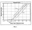
- Figure 2 is a graphical analysis of the reaction force of the poke-in contact.
- Figure 3 is a graphical analysis of the stress upon the contact of the present invention.
- the present invention is directed to a poke-in contact mount assembly that reduces the normal forces sustained by the circuit board and components during insertion of the wire tabbing into the junction box.
- FIGS 1A, 1B , 1C and 1D illustrate various views of the poke-in contact 10 used in the present invention.
- the poke-in contact 10 includes a base section 51, with generally upstanding wall sections 52 that extend perpendicular and upward from the base 51 to form parallel opposite walls.
- a top section 54 extends and spans the distance between both wall sections 52.
- the base 51, wall sections 52 and top section 54 form a box-like structure, having four defined areas connecting to enclose a space.
- a locking lance 30 Extending from the top section 54 and wrapping around in an arcuate shape, a locking lance 30 contains three portions, a back section 56, a contact beam 50 and a front section 58.
- the back section 56 forms a hemi circular shape similar in cross-section to a half circle before it transitions into the contact beam 50.
- the contact beam 50 is adjacent to and parallel to the base 51, but not contacting the base 51.
- the contact beam 50 extends the entire length of the base 51 and turns upward forming a front section 58 that angles in toward the center of the poke-in contact 10.
- the front section 58 preferably rests at an angle of approximately forty-five degrees from the contact beam 50, but any other suitable angle may be used.
- the poke-in contact 10 can be constructed of copper, a copper alloy, or any other suitable material that is electrically conductive, substantially flexible to accept an insert, while being substantially sturdy and rigid to provide retention when force is applied.
- the alloy may be of thickness of about 0.35 mm thick, but can be constructed with any thickness suitable for the contact 10 to operate correctly with the required retention.
- Figure 1A illustrates a perspective view of the top of the poke-in contact assembly 10.
- a wall aperture 38 is located, where a portion of the locking lance 30 protrudes.
- the protrusion 40 of the locking lance 30 through this wall aperture 38 provides the ability to deflect the lance 30 with a tool or utensil when necessary to remove the wire or conductive material that is secured in the poke-in contact 10.
- the wall apertures 38 also acts as a check device to ensure that the front section 58 of the lance 30 is not displaced to an angle that would cause damage to the lance 30.
- Figure 1B illustrates a perspective view of the bottom of the contact 10.
- the solder pin tails 18 are disposed to secure the contact 10 to the printed circuit board 12 by a solder connection or other suitable connection.
- Figure 1C illustrates the surface area and shape of the present invention in an intermediate form, as the assembly is initially stamped from sheet stock. The wall apertures 38 are shown, along with the protrusions 40 on the lance 30. In addition the solder pin tails 18 are also disposed along the edges of the contact 10.
- Figure 1C shows the poke-in contact 10 being of unitary construction and stamped to form the base 51, walls 52, top 54, and lance 30 of the contact 10 as depicted in Figures 1A and 1B . It should be known that the poke-in contact may also be manufactured and assembled from more than one unitary piece.
- Figure 1D illustrates a cross sectional view of the poke-in contact 10 of Figure 1A .
- the printed circuit board 12 receives the solder pin tails 18 of the contact 10, where they are secured into place by solder or other similar connection.
- a wire tabbing 42 enters the poke-in contact 10 by pushing against the front section 58 of the lance 30.
- the front section 58 of the lance 30 deflects to receive the wire tabbing 42 by displacing the contact beam 51 toward the base 28 of the contact 10 while maintaining a firm tension on the wire tabbing 42 to secure the wire tabbing 42 in place.
- the lance 30 When an opposite force is applied to the wire tabbing 42, such as a force to remove the tabbing 42 from the lance 30, the lance 30 provides a preselected range of retention, preferable ten to fifteen pounds.
- the force can be adjusted by angle selection, material selection, material thickness and the size of the contact 10. In effect, as resistance is created against the lance 30, the lance 30 responds with a greater force, an equal and opposite force against the tabbing, to secure the wire up to fifteen pounds of force.
- a tool such as a screwdriver, a similar device or other suitable tool can be used to contact the protrusions 40 of the lance 30, releasing the contact of the lance 30 and the tabbing 42, and allowing the tabbing 42 to retract from the contact 10.
- the protrusions 40 are forced away from the top 54 by the tabbing 42, creating a space between the wire tabbing 42 and the front section 58 of the lance 30 and allowing the wire tabbing 42 to be removed with no reaction force applied by the lance 30.
- the inserted structure is not limited to tabbing as shown and can include wire.
- Figure 2 graphically illustrates the reaction force during displacement of the lance 30 on a wire tabbing 42 inserted into the contact 10.
- the displacement of the lance 30 is relatively low and constant.
- the contact beam 50 is not in contact with the base 51 of the poke-in contact 10 (See Figure 1D ).
- the front end 58 of the lance 30 moves inwardly and downwardly toward the contact beam 50.
- the lance 30 displaces downward as the wire tabbing is inserted until the contact beam 50 touches the base 51 of the poke-in contact 10.
- the displacement downwardly is limited by the base 51 and causes the end 58 to exert a force against the tabbing 42.
- the reaction force and displacement increases as more force is applied to insert the wire tabbing 42 into the poke-in contact 10.
- the front end 58 of the lance 30 begins to compress and displace as the contact beam 50 and back section 56 do not displace any further.
- the maximum force and displacement the lance 30 can endure without breaking is shown at point 74 in Figure 2 which is the course related to the ultimate tensile strength (UTS) of the material selected. It is preferred to maintain displacement that is less than the UTS to prevent deformation of the lance and the contact.
- UTS ultimate tensile strength
- the lance 30 will remain at the maximum displacement (shown by point 74) until the protrusions 40 of the lance 30 are released, and the wire tabbing 42 is removed.
- Section 72 in Figure 2 shows the reduction in displacement and reaction force as the wire tabbing 42 is removed from the lance 30.
- Figure 3 illustrates the stresses on the locking lance 30 during insertion of the wire tabbing 42.
- the analysis was taken during insertion of a wire tabbing (not shown) where the maximum stress is applied to the lance 30.
- the contact 10 In the uncompressed position, when the contact 10 is not receiving wire tabbing, and no stresses are placed on the lance 30 and the contact beam 50 is not in contact with the base 51 of the contact 10. Only when the wire tabbing 42 is inserted into the lance 30 do sufficient stresses begin to occur to move the contact beam 50 into contact with the base 51 in a terminal connection.
- the back section 56 of the lance 30 does not sustain any stresses, as the normal force of the wire tabbing is inserted into the lance 30 is resolved as a vertical force and is applied in the front section 58 of the lance 30 closest to the wire tabbing 42 and in the area of the lance 30 that is flexing the most.
- the normal force of the wire tabbing 42 being inserted into the contact 10 by pushing down on the lance 30 results in stresses at the front side 58 of the lance 10 and pushes the contact beam 50 downward to make a terminal connection to the base 51 below.
- the poke-in contact assembly provides a secure connection for wire tabbing that does not require the use of tools or other utensils when inserting.
- the lance of the poke-in contact displaces upon insertion of the wire tabbing and absorbs the majority of the force applied by the tabbing, thereby reducing the amount of force applied to the printed circuit board or other device the contact is mounted to.
- the poke-in contact applies a force or retention when the tabbing is forced outward from the poke-in contact without the use of tools or other utensils.
- a tool or utensil is used to depress the lance and release the tabbing and the force applied to the tabbing by the lance.
Landscapes
- Coupling Device And Connection With Printed Circuit (AREA)
- Multi-Conductor Connections (AREA)
Abstract
Description
- The present invention is directed to an improved system and method for securing electronics in a junction box. More specifically, the present invention is directed to a contact assembly for securing electronics in a junction box without the use of tools or other equipment.
- Most commonly, current systems use fragile electronics disposed in the junction boxes. The electronic components are unable to sustain the forces of inserting wire tabbing into the connections within the junction box. Often times the electronics are damaged or the solder connections are broken from the force of repeatedly inserting and removing the wire tabbing into the junction box. One current system redesigned the typical junction box by adding a second capsule around the body section of the entire contact body to help remedy the issue of the force when inserting the wire tabbing. The second capsule provides extra support and strength to withstand the normal force from inserting the wire tabbing into the junction box when making an electrical connection. However, this system requires more materials for manufacture, is more expensive and requires a longer assembly time.
- Other current methods eliminate the second outer capsule discussed above, where the junction box is constructed of material strong enough to withstand the normal force applied during insertion of the wire tabbing. However, in order to maintain a solid connection with the wire tabbing, these systems require the aid and use of tools or equipment to initiate the connection with the wire tabbing. The use of the tools and equipment to make the connection is time consuming, as well as expensive. In addition, often times, these tool connections are permanent and prevent the replacement of any of the components.
- In addition, the wire tabbing used to make electrical connections with the electronics within the junction box are connected with a solder connection which is time consuming and expensive when both designing and repairing the system.
JP 09 073927 - Thus, what is needed is a system that is configured with a receptacle that is capable of receiving wire tabbing and strong enough to withstand the normal force of insertion. A system that allows for easy repairs and replacement when necessary to reduce time and costs is needed as well.
- The present invention is a connector assembly for receiving an electrical component according to
claim 1. - One advantage of the present invention is the lower manufacturing, replacement and maintenance costs of the system.
- Yet another advantage of the present invention is improved replaceability functionality.
- Another advantage of the present invention is that no tools or equipment are necessary to electrically connect the wire tabbing in the poke-in contact.
- Yet another advantage of the present invention is that no support apparatuses are required for the contact.
- Another advantage of the present invention is high retention of the contact.
- Another advantage of the present invention is that the present invention can replace the circuitry in current systems with little or substantially zero modifications to the circuitry exterior to the junction box.
- Yet another advantage of the present invention is low normal force applied during insertion of the wire tabbing into the poke-in contact.
- Another advantage of the present invention is the locking mechanism of the lance once the wire tabbing is inserted into the poke-in contact.
- Other features and advantages of the present invention will be apparent from the following more detailed description of the preferred embodiment, taken in conjunction with the accompanying drawings which illustrate, by way of example, the principles of the invention.
-
Figure 1A illustrates a perspective view of the top of the present invention. -
Figure 1B illustrates a perspective view of the bottom of the present invention. -
Figure 1C illustrates a surface area view of the present invention. -
Figure 1D illustrates a cross sectional view of the contact of the present invention. -
Figure 2 is a graphical analysis of the reaction force of the poke-in contact. -
Figure 3 is a graphical analysis of the stress upon the contact of the present invention. - The present invention is directed to a poke-in contact mount assembly that reduces the normal forces sustained by the circuit board and components during insertion of the wire tabbing into the junction box.
-
Figures 1A, 1B ,1C and 1D illustrate various views of the poke-incontact 10 used in the present invention. As shown inFigures 1A and 1B , the poke-incontact 10 includes abase section 51, with generallyupstanding wall sections 52 that extend perpendicular and upward from thebase 51 to form parallel opposite walls. Parallel to thebase 51 and connected on the opposite end of thewall sections 52 than thebase 51, atop section 54 extends and spans the distance between bothwall sections 52. Thebase 51,wall sections 52 andtop section 54 form a box-like structure, having four defined areas connecting to enclose a space. Extending from thetop section 54 and wrapping around in an arcuate shape, alocking lance 30 contains three portions, aback section 56, acontact beam 50 and afront section 58. Theback section 56 forms a hemi circular shape similar in cross-section to a half circle before it transitions into thecontact beam 50. Thecontact beam 50 is adjacent to and parallel to thebase 51, but not contacting thebase 51. Thecontact beam 50 extends the entire length of thebase 51 and turns upward forming afront section 58 that angles in toward the center of the poke-incontact 10. Thefront section 58 preferably rests at an angle of approximately forty-five degrees from thecontact beam 50, but any other suitable angle may be used. The poke-incontact 10 can be constructed of copper, a copper alloy, or any other suitable material that is electrically conductive, substantially flexible to accept an insert, while being substantially sturdy and rigid to provide retention when force is applied. The alloy may be of thickness of about 0.35 mm thick, but can be constructed with any thickness suitable for thecontact 10 to operate correctly with the required retention. -
Figure 1A illustrates a perspective view of the top of the poke-incontact assembly 10. On each of thewall sections 52, awall aperture 38 is located, where a portion of the locking lance 30 protrudes. Theprotrusion 40 of the locking lance 30 through thiswall aperture 38 provides the ability to deflect thelance 30 with a tool or utensil when necessary to remove the wire or conductive material that is secured in the poke-incontact 10. Thewall apertures 38 also acts as a check device to ensure that thefront section 58 of thelance 30 is not displaced to an angle that would cause damage to thelance 30. -
Figure 1B illustrates a perspective view of the bottom of thecontact 10. Thesolder pin tails 18 are disposed to secure thecontact 10 to the printedcircuit board 12 by a solder connection or other suitable connection.Figure 1C illustrates the surface area and shape of the present invention in an intermediate form, as the assembly is initially stamped from sheet stock. Thewall apertures 38 are shown, along with theprotrusions 40 on thelance 30. In addition thesolder pin tails 18 are also disposed along the edges of thecontact 10.Figure 1C shows the poke-incontact 10 being of unitary construction and stamped to form thebase 51,walls 52,top 54, and lance 30 of thecontact 10 as depicted inFigures 1A and 1B . It should be known that the poke-in contact may also be manufactured and assembled from more than one unitary piece. -
Figure 1D illustrates a cross sectional view of the poke-incontact 10 ofFigure 1A . The printedcircuit board 12 receives thesolder pin tails 18 of thecontact 10, where they are secured into place by solder or other similar connection. Awire tabbing 42 enters the poke-incontact 10 by pushing against thefront section 58 of thelance 30. Thefront section 58 of thelance 30 deflects to receive thewire tabbing 42 by displacing thecontact beam 51 toward the base 28 of thecontact 10 while maintaining a firm tension on thewire tabbing 42 to secure thewire tabbing 42 in place. When an opposite force is applied to thewire tabbing 42, such as a force to remove thetabbing 42 from thelance 30, thelance 30 provides a preselected range of retention, preferable ten to fifteen pounds. The force can be adjusted by angle selection, material selection, material thickness and the size of thecontact 10. In effect, as resistance is created against thelance 30, thelance 30 responds with a greater force, an equal and opposite force against the tabbing, to secure the wire up to fifteen pounds of force. To easily and quickly remove thetabbing 42 from the contact, a tool such as a screwdriver, a similar device or other suitable tool can be used to contact theprotrusions 40 of thelance 30, releasing the contact of thelance 30 and thetabbing 42, and allowing thetabbing 42 to retract from thecontact 10. Theprotrusions 40 are forced away from the top 54 by the tabbing 42, creating a space between the wire tabbing 42 and thefront section 58 of thelance 30 and allowing the wire tabbing 42 to be removed with no reaction force applied by thelance 30. The inserted structure is not limited to tabbing as shown and can include wire. -
Figure 2 graphically illustrates the reaction force during displacement of thelance 30 on a wire tabbing 42 inserted into thecontact 10. As shown inportion 70 ofFigure 2 , the displacement of thelance 30 is relatively low and constant. Before the wire tabbing 42 is inserted into the poke-incontact 10, thecontact beam 50 is not in contact with thebase 51 of the poke-in contact 10 (SeeFigure 1D ). As the wire tabbing is inserted into thelance 30, thefront end 58 of thelance 30 moves inwardly and downwardly toward thecontact beam 50. Thelance 30 displaces downward as the wire tabbing is inserted until thecontact beam 50 touches thebase 51 of the poke-incontact 10. The displacement downwardly is limited by thebase 51 and causes theend 58 to exert a force against the tabbing 42. As shown atpoint 76 inFigure 2 , the reaction force and displacement increases as more force is applied to insert the wire tabbing 42 into the poke-incontact 10. Once thecontact beam 50 is in full contact with thebase 51 of the poke-incontact 10, thefront end 58 of thelance 30 begins to compress and displace as thecontact beam 50 and backsection 56 do not displace any further. The maximum force and displacement thelance 30 can endure without breaking is shown atpoint 74 inFigure 2 which is the course related to the ultimate tensile strength (UTS) of the material selected. It is preferred to maintain displacement that is less than the UTS to prevent deformation of the lance and the contact. Thelance 30 will remain at the maximum displacement (shown by point 74) until theprotrusions 40 of thelance 30 are released, and the wire tabbing 42 is removed.Section 72 inFigure 2 shows the reduction in displacement and reaction force as the wire tabbing 42 is removed from thelance 30. -
Figure 3 illustrates the stresses on thelocking lance 30 during insertion of the wire tabbing 42. The analysis was taken during insertion of a wire tabbing (not shown) where the maximum stress is applied to thelance 30. In the uncompressed position, when thecontact 10 is not receiving wire tabbing, and no stresses are placed on thelance 30 and thecontact beam 50 is not in contact with thebase 51 of thecontact 10. Only when the wire tabbing 42 is inserted into thelance 30 do sufficient stresses begin to occur to move thecontact beam 50 into contact with the base 51 in a terminal connection. Theback section 56 of thelance 30 does not sustain any stresses, as the normal force of the wire tabbing is inserted into thelance 30 is resolved as a vertical force and is applied in thefront section 58 of thelance 30 closest to the wire tabbing 42 and in the area of thelance 30 that is flexing the most. The normal force of the wire tabbing 42 being inserted into thecontact 10 by pushing down on thelance 30 results in stresses at thefront side 58 of thelance 10 and pushes thecontact beam 50 downward to make a terminal connection to thebase 51 below. - The poke-in contact assembly provides a secure connection for wire tabbing that does not require the use of tools or other utensils when inserting. The lance of the poke-in contact displaces upon insertion of the wire tabbing and absorbs the majority of the force applied by the tabbing, thereby reducing the amount of force applied to the printed circuit board or other device the contact is mounted to. In addition, the poke-in contact applies a force or retention when the tabbing is forced outward from the poke-in contact without the use of tools or other utensils. To effectively remove the tabbing from the contact, a tool or utensil is used to depress the lance and release the tabbing and the force applied to the tabbing by the lance.
- While the invention has been described with reference to a preferred embodiment, it will be understood by those skilled in the art that various changes may be made and equivalents may be substituted for elements thereof without departing from the scope of the invention. In addition, many modifications may be made to adapt a particular situation or material to the teachings of the invention without departing from the essential scope thereof. Therefore, it is intended that the invention not be limited to the particular embodiment disclosed as the best mode contemplated for carrying out this invention, but that the invention will include all embodiments falling within the scope of the appended claims.
Claims (12)
- A connector assembly (10) for receiving an electrical component (42), The connector assembly comprising:a base (51);a plurality of pin tails (18), each pin tail of the plurality of pin tails extending in a substantially perpendicular direction away from the base and configured to connect to a printed circuit board (12);a plurality of walls (52) each wall of the plurality of walls extending from the base in an opposed direction of the plurality of pin tails;a top (54) disposed to extend between the plurality of walls and substantially parallel to the base;a lance (30) the lance being disposed to extend from the top and further comprising:an arcuate back end (56);a contact beam (50) that extends parallel to the base;a front section (58) disposed at a preselected angle to the contact beam;at least one protrusion (40) extending from the front section; andwherein the electrical component is manually insertable into the connector assembly with an insertion force, pressing against the front section, which moves upon insertion of the electrical component, wherein upon displacement, the contact beam touches the base to complete an electrically conductive connection, and wherein, when inserted in the connector assembly, the electrical component is secured in the connector until a force is applied to the at least one protrusion extending from the the front section.
- The connector assembly of claim 1 wherein the electrical component is manually insertable into the connector assembly without the aid of an additional device.
- The connector assembly of claim 1 wherein the lance exerts an equal and opposite reactive force upon the electrical component to secure the electrical component in the connector assembly.
- The connector assembly of claim 1 wherein at least one pin tail of the plurality of pin tails can be connected to the printed circuit board by a weld connection.
- The connector assembly of claim 1 wherein the electrical component is releasable by the force applied to the at least one protrusion using a tool or utensil.
- The connector assembly of claim 1 wherein the contact beam substantially absorbs the insertion force of the electrical component.
- The connector assembly of claim 1, wherein the connector assembly is a poke-in contact assembly, and wherein the lance exerts an equal and opposite reactive force upon the electrical component to secure the electrical component in the connector assembly.
- The connector assembly of claim 7 wherein the protrusion is manually inserted into the connector assembly without the aid of an additional device.
- The connector assembly of claim 7 wherein the electrical component-is releasable by a force applied to the at least one protrusion thereby releasing the equal and opposite reactive force upon the electrical component.
- The connector assembly of claim 7 wherein at least one pin tail of the plurality of pin tails is connected to the printed circuit board by a weld connection.
- The connector assembly of claim 7 wherein the lance applies a reactive force when the protrusion applies a force against the lance without the use of tools or untensils.
- The connector assembly of claim 11 wherein the force applied to the at least one protrusion is applied with the use of a tool or utensil.
Applications Claiming Priority (2)
| Application Number | Priority Date | Filing Date | Title |
|---|---|---|---|
| US11/550,148 US7351118B1 (en) | 2006-10-17 | 2006-10-17 | Poke-in contacts for modular PCB assembly |
| PCT/US2007/021186 WO2008048420A2 (en) | 2006-10-17 | 2007-10-02 | Poke-in contacts for modular pcb assembly |
Publications (2)
| Publication Number | Publication Date |
|---|---|
| EP2082453A2 EP2082453A2 (en) | 2009-07-29 |
| EP2082453B1 true EP2082453B1 (en) | 2010-01-27 |
Family
ID=39227238
Family Applications (1)
| Application Number | Title | Priority Date | Filing Date |
|---|---|---|---|
| EP07839165A Active EP2082453B1 (en) | 2006-10-17 | 2007-10-02 | Poke-in contacts for modular pcb assembly |
Country Status (5)
| Country | Link |
|---|---|
| US (1) | US7351118B1 (en) |
| EP (1) | EP2082453B1 (en) |
| CN (1) | CN101529659B (en) |
| DE (1) | DE602007004646D1 (en) |
| WO (1) | WO2008048420A2 (en) |
Families Citing this family (9)
| Publication number | Priority date | Publication date | Assignee | Title |
|---|---|---|---|---|
| DE102008048087A1 (en) * | 2008-09-19 | 2010-04-08 | Phoenix Contact Gmbh & Co. Kg | Electrical device, has spring force clamp with clamping arm that is provided for clamping electrical conductor, and conductor support for supporting electrical conductor and provided in spring force clamp |
| IT1398659B1 (en) * | 2009-06-15 | 2013-03-08 | Manca | LOW COST CLAMP FOR ELECTRICAL / ELECTRONIC APPLICATIONS ON PRINTED CIRCUIT |
| DE102013109802A1 (en) * | 2013-09-09 | 2015-03-12 | Phoenix Contact Gmbh & Co. Kg | clamping spring |
| DE102015115791B4 (en) * | 2015-09-18 | 2017-05-04 | Wago Verwaltungsgesellschaft Mbh | Wire connecting terminal element |
| DE202015104962U1 (en) * | 2015-09-18 | 2016-12-21 | Wago Verwaltungsgesellschaft Mbh | Conductor terminal |
| DE202017101148U1 (en) * | 2017-03-01 | 2018-06-04 | Wago Verwaltungsgesellschaft Mbh | Wire connecting terminal element |
| DE102019125886B4 (en) * | 2019-09-26 | 2021-06-17 | Bjb Gmbh & Co. Kg | Housing-free connection terminal with opening tool |
| WO2023242316A1 (en) * | 2022-06-16 | 2023-12-21 | Valeo Systemes Thermiques | Mechanical component for electrical contact, and corresponding control module and motor-fan assembly |
| DE102023212395A1 (en) * | 2023-12-08 | 2025-06-12 | Robert Bosch Gesellschaft mit beschränkter Haftung | Connector device and corresponding manufacturing process |
Family Cites Families (12)
| Publication number | Priority date | Publication date | Assignee | Title |
|---|---|---|---|---|
| US4422128A (en) * | 1981-08-06 | 1983-12-20 | General Motors Corporation | Push-on terminal clip and assembly |
| US5424918A (en) * | 1994-03-31 | 1995-06-13 | Hewlett-Packard Company | Universal hybrid mounting system |
| US5494456A (en) * | 1994-10-03 | 1996-02-27 | Methode Electronics, Inc. | Wire-trap connector with anti-overstress member |
| JP3017433B2 (en) * | 1995-09-05 | 2000-03-06 | 株式会社八光電機製作所 | Terminal device |
| EP0762551B1 (en) * | 1995-09-12 | 2002-10-16 | The Whitaker Corporation | Electrical terminal with locking lance |
| US6062918A (en) * | 1996-07-01 | 2000-05-16 | The Whitaker Corporation | Electrical receptacle contact assembly |
| US6464547B2 (en) * | 2000-02-18 | 2002-10-15 | Tyco Electronics Corporation | Electrical pin contact and housing |
| US6629865B2 (en) * | 2001-12-07 | 2003-10-07 | Delphi Technologies, Inc. | Zero terminal insertion force electrical connection assembly |
| US6461200B1 (en) * | 2001-12-11 | 2002-10-08 | Hon Hai Precision Ind. Co., Ltd. | Electrical connector assembly |
| US6926541B2 (en) * | 2002-08-30 | 2005-08-09 | Yazaki Corporation | Mounting structure of electric junction box |
| JP3828486B2 (en) * | 2002-12-09 | 2006-10-04 | ヒロセ電機株式会社 | Electrical connector with square tube case |
| TWM246674U (en) * | 2003-11-21 | 2004-10-11 | Hon Hai Prec Ind Co Ltd | Clip for heat sink |
-
2006
- 2006-10-17 US US11/550,148 patent/US7351118B1/en active Active
-
2007
- 2007-10-02 CN CN2007800388640A patent/CN101529659B/en active Active
- 2007-10-02 EP EP07839165A patent/EP2082453B1/en active Active
- 2007-10-02 WO PCT/US2007/021186 patent/WO2008048420A2/en not_active Ceased
- 2007-10-02 DE DE602007004646T patent/DE602007004646D1/en active Active
Also Published As
| Publication number | Publication date |
|---|---|
| US7351118B1 (en) | 2008-04-01 |
| EP2082453A2 (en) | 2009-07-29 |
| DE602007004646D1 (en) | 2010-03-18 |
| WO2008048420A2 (en) | 2008-04-24 |
| CN101529659A (en) | 2009-09-09 |
| WO2008048420A3 (en) | 2008-06-12 |
| US20080090471A1 (en) | 2008-04-17 |
| CN101529659B (en) | 2011-04-20 |
Similar Documents
| Publication | Publication Date | Title |
|---|---|---|
| EP2082453A2 (en) | Poke-in contacts for modular pcb assembly | |
| US6305949B1 (en) | Press-fit pin, connector and printed circuit board-connected structure | |
| EP0825680A2 (en) | Deformable pin electrical connector | |
| JP5292582B2 (en) | Spring terminal, structure, and method for assembling a spring terminal | |
| EP0427563A2 (en) | Apparatus and method for installation of multi-pin components on circuit boards | |
| KR101504696B1 (en) | Contact device for fastening to a circuit board, method for fastening a contact device to a circuit board, and circuit board | |
| US20030114027A1 (en) | Simplified board connector | |
| EP0801821A1 (en) | Electrical connector | |
| EP2568536A1 (en) | Bending coaxial electric connector | |
| WO1997032362A1 (en) | Compliant section for electrical terminal mounted to a circuit board | |
| US10374337B2 (en) | Terminal block | |
| EP2012393B1 (en) | Surface mount contact member | |
| US7101197B2 (en) | Press-fit terminal, printed board connection structure using the press-fit terminal, and electrical connection box | |
| EP0499431B1 (en) | Lanced hold-downs | |
| CN101409416A (en) | High density flexible socket interconnect system | |
| JPH09204944A (en) | Stacked electric connector assembly | |
| EP0422744B1 (en) | A latching means and an electrical circuit component with such a latching means for mounting to a substrate | |
| EP0836244B1 (en) | Electrical connector for mounting on the surface of a printed circuit board | |
| US6139362A (en) | Fastener for connecting an electrical device to a substrate | |
| US7416446B2 (en) | Connector | |
| CN100452543C (en) | Terminal connection structure, electrical junction box having the terminal connection structure, and method for assembling the electrical junction box | |
| JP2007087621A (en) | Wire connection connector | |
| US7520787B2 (en) | Electrical connection of a contact pin to a sheet metal component | |
| EP1646113A2 (en) | Cable connector | |
| JP2009266411A (en) | Jack connector, and portable terminal equipped with it |
Legal Events
| Date | Code | Title | Description |
|---|---|---|---|
| PUAI | Public reference made under article 153(3) epc to a published international application that has entered the european phase |
Free format text: ORIGINAL CODE: 0009012 |
|
| 17P | Request for examination filed |
Effective date: 20090326 |
|
| AK | Designated contracting states |
Kind code of ref document: A2 Designated state(s): DE FR GB |
|
| GRAP | Despatch of communication of intention to grant a patent |
Free format text: ORIGINAL CODE: EPIDOSNIGR1 |
|
| DAX | Request for extension of the european patent (deleted) | ||
| GRAS | Grant fee paid |
Free format text: ORIGINAL CODE: EPIDOSNIGR3 |
|
| GRAA | (expected) grant |
Free format text: ORIGINAL CODE: 0009210 |
|
| AK | Designated contracting states |
Kind code of ref document: B1 Designated state(s): DE FR GB |
|
| REG | Reference to a national code |
Ref country code: GB Ref legal event code: FG4D |
|
| REF | Corresponds to: |
Ref document number: 602007004646 Country of ref document: DE Date of ref document: 20100318 Kind code of ref document: P |
|
| PLBE | No opposition filed within time limit |
Free format text: ORIGINAL CODE: 0009261 |
|
| STAA | Information on the status of an ep patent application or granted ep patent |
Free format text: STATUS: NO OPPOSITION FILED WITHIN TIME LIMIT |
|
| 26N | No opposition filed |
Effective date: 20101028 |
|
| PG25 | Lapsed in a contracting state [announced via postgrant information from national office to epo] |
Ref country code: FR Free format text: LAPSE BECAUSE OF NON-PAYMENT OF DUE FEES Effective date: 20101102 |
|
| REG | Reference to a national code |
Ref country code: FR Ref legal event code: ST Effective date: 20110630 |
|
| GBPC | Gb: european patent ceased through non-payment of renewal fee |
Effective date: 20111002 |
|
| PG25 | Lapsed in a contracting state [announced via postgrant information from national office to epo] |
Ref country code: GB Free format text: LAPSE BECAUSE OF NON-PAYMENT OF DUE FEES Effective date: 20111002 |
|
| REG | Reference to a national code |
Ref country code: DE Ref legal event code: R082 Ref document number: 602007004646 Country of ref document: DE Representative=s name: MARKS & CLERK (LUXEMBOURG) LLP, LU Ref country code: DE Ref legal event code: R081 Ref document number: 602007004646 Country of ref document: DE Owner name: TE CONNECTIVITY CORPORATION, BERWYN, US Free format text: FORMER OWNER: TYCO ELECTRONICS CORP., BERWYN, PA., US |
|
| PGFP | Annual fee paid to national office [announced via postgrant information from national office to epo] |
Ref country code: DE Payment date: 20250902 Year of fee payment: 19 |