EP2081308A1 - Method and device for providing and/or controlling an optical signal - Google Patents
Method and device for providing and/or controlling an optical signal Download PDFInfo
- Publication number
- EP2081308A1 EP2081308A1 EP08000698A EP08000698A EP2081308A1 EP 2081308 A1 EP2081308 A1 EP 2081308A1 EP 08000698 A EP08000698 A EP 08000698A EP 08000698 A EP08000698 A EP 08000698A EP 2081308 A1 EP2081308 A1 EP 2081308A1
- Authority
- EP
- European Patent Office
- Prior art keywords
- signal
- optical
- absorber
- limiter
- light source
- Prior art date
- Legal status (The legal status is an assumption and is not a legal conclusion. Google has not performed a legal analysis and makes no representation as to the accuracy of the status listed.)
- Granted
Links
Images


Classifications
-
- H—ELECTRICITY
- H04—ELECTRIC COMMUNICATION TECHNIQUE
- H04B—TRANSMISSION
- H04B10/00—Transmission systems employing electromagnetic waves other than radio-waves, e.g. infrared, visible or ultraviolet light, or employing corpuscular radiation, e.g. quantum communication
- H04B10/25—Arrangements specific to fibre transmission
- H04B10/2507—Arrangements specific to fibre transmission for the reduction or elimination of distortion or dispersion
- H04B10/2537—Arrangements specific to fibre transmission for the reduction or elimination of distortion or dispersion due to scattering processes, e.g. Raman or Brillouin scattering
-
- H—ELECTRICITY
- H04—ELECTRIC COMMUNICATION TECHNIQUE
- H04B—TRANSMISSION
- H04B10/00—Transmission systems employing electromagnetic waves other than radio-waves, e.g. infrared, visible or ultraviolet light, or employing corpuscular radiation, e.g. quantum communication
- H04B10/29—Repeaters
- H04B10/291—Repeaters in which processing or amplification is carried out without conversion of the main signal from optical form
- H04B10/2912—Repeaters in which processing or amplification is carried out without conversion of the main signal from optical form characterised by the medium used for amplification or processing
- H04B10/2916—Repeaters in which processing or amplification is carried out without conversion of the main signal from optical form characterised by the medium used for amplification or processing using Raman or Brillouin amplifiers
-
- H—ELECTRICITY
- H04—ELECTRIC COMMUNICATION TECHNIQUE
- H04B—TRANSMISSION
- H04B10/00—Transmission systems employing electromagnetic waves other than radio-waves, e.g. infrared, visible or ultraviolet light, or employing corpuscular radiation, e.g. quantum communication
- H04B10/29—Repeaters
- H04B10/291—Repeaters in which processing or amplification is carried out without conversion of the main signal from optical form
- H04B10/293—Signal power control
- H04B10/294—Signal power control in a multiwavelength system, e.g. gain equalisation
- H04B10/296—Transient power control, e.g. due to channel add/drop or rapid fluctuations in the input power
-
- H—ELECTRICITY
- H04—ELECTRIC COMMUNICATION TECHNIQUE
- H04J—MULTIPLEX COMMUNICATION
- H04J14/00—Optical multiplex systems
- H04J14/02—Wavelength-division multiplex systems
- H04J14/0221—Power control, e.g. to keep the total optical power constant
- H04J14/02216—Power control, e.g. to keep the total optical power constant by gain equalization
-
- H—ELECTRICITY
- H04—ELECTRIC COMMUNICATION TECHNIQUE
- H04B—TRANSMISSION
- H04B2210/00—Indexing scheme relating to optical transmission systems
- H04B2210/25—Distortion or dispersion compensation
- H04B2210/256—Distortion or dispersion compensation at the repeater, i.e. repeater compensation
Definitions
- the invention relates to a method and to a device for providing and/or controlling an optical signal.
- Groups of optical signals with various wavelengths are transmitted via optical fibers utilizing in particular optical transmission amplifiers.
- WDM wavelength division multiplex
- Raman gain In optical transmission systems, a particular nonlinearity is known as a Raman gain or Raman effect, which is a nonlinear scattering process and results in a power transfer from shorter wavelength channels to longer wavelength channels.
- the Raman gain becomes significant when a particular level of optical power distributed over a range of wavelengths is pumped into an optical fiber. In such case, the Raman gain is tilted in favor of the channels having the longer wavelengths. This undesired effect is referred to as Raman tilt.
- This tilt described in dB/THz, is in a good approximation proportional to the total optical power fed into the fiber. Fast variation of total optical power results in fast variation of Raman induced tilt and constant total optical power results in constant Raman tilt, which can be simply compensated by tilted amplifiers or filters.
- SRS Stimulated Raman Scattering
- the Stimulated Raman Scattering has an impact on a level of the channels at the end of the optical fiber and hence at the input of a receiver or amplifier. For example, dropping “red” channels or a breach of fiber may result in the "blue” channels having a level beyond the input range of the amplifier.
- the transmission fiber may show an increased degree of nonlinear distortion.
- the problem to be solved is to overcome the disadvantages stated before and in particular to provide an efficient approach to compensate detrimental effects in an optical transmission system by enabling a pure optical solution without any electro-optical converter or electronic control circuitry.
- This approach allows maintaining a constant power level of the combined signal that may be supplied, e.g., at an output of a device or optical circuit arrangement.
- said combined signal is processed by optical means, i.e. without any electro-optical converter or electronic control circuitry.
- an optical power of the control signal is at least partially supplied by a light source, in particular a laser.
- At least one wavelength of the light source is disjoint to at least one wavelength utilized for the at least one data signal.
- the data signal may comprise several channels, wherein wavelengths utilized for the data signal are in particular disjoint from the wavelength used by the light source.
- the light source comprises a Raman tilt control laser.
- the optical signal of the light source and the at least one data signal are fed to an optical limiter in order to obtain the combined signal.
- the optical limiter processes the signals provided in particular by limiting an output power to a predefined threshold "lim". Below such threshold value the input power may substantially equal the output power of the limiter.
- optical signal of the light source and the at least one data signal are fed to the optical limiter via a circulator or via a coupler.
- the optical limiter comprises a semiconductor optical amplifier (SOA).
- SOA semiconductor optical amplifier
- an output of the optical limiter is processed by an absorber and then combined with the data signal into said combined signal.
- a filter may process the input signal of the absorber, wherein said filter may advantageously have a substantially inverse characteristics of the absorber.
- the absorber may in particular be a saturable absorber.
- the absorber comprises a semiconductor optical amplifier (SOA) or an erbium doped fiber amplifier (EDFA).
- SOA semiconductor optical amplifier
- EDFA erbium doped fiber amplifier
- the EDFA in an absorber may in particular be used to adjust a threshold of its limiting power.
- control signal compensates at least partially a Raman tilt and/or a Raman gain.
- the data signal is coupled with the output of the limiter to provide said combined signal.
- the data signal is coupled via an attenuator, in particular via an adjustable attenuator, with the output of the limiter to provide said combined signal.
- the output of the limiter is fed to an absorber, wherein the output of said absorber provides (an optical power of) a control signal portion of the combined signal.
- a filter is provided before the absorber, wherein said filter in particular shows a substantially inverse characteristics of the absorber.
- a circulator is provided to combine the data signal and the signal from the light source.
- a coupler may be provided to combine the data signal and the signal from the light source.
- the device may be used in or part of an optical transmission system, said system comprising at least one semiconductor optical amplifier (SOA) for suppressing and/or reducing noise and/or interference by cross gain modulation.
- SOA semiconductor optical amplifier
- such device may comprise at least one switch that is based on or realized by at least one semiconductor optical amplifier (SOA).
- SOA semiconductor optical amplifier
- EDFA erbium doped fiber amplifier
- the remaining data signals sustain their respective power level.
- equation (3) can be met by providing at least two signal paths:
- the wavelength utilized by a control laser supplying the optical power to the control path is disjoint to the wavelengths of the data signals (channels).
- the saturable absorber subtracts a constant amount of light power from the signal and may hence be utilized to remove a constant offset from the signal. This is in particular useful to remove an offset of a control laser that is set to full level.
- Embodiments without such saturable absorber will be referred to in more detail below.
- An absorber may in particular be realized by an erbium doped (Er 3+ ) glass fiber allowing for a time delay in a range of 100s of milliseconds.
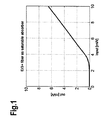
- a transfer characteristics of a typically doped glass fiber used as saturable absorber is shown in Fig.1 .
- such an erbium doped glass fiber may require a filter put in front of the absorber comprising an inverse characteristics of the saturable absorber.
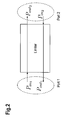
- Fig.2 shows the corresponding quadripole of the limiter.
- the indices in equations (4.1) and (4.2) may refer to different directions of a signal or to different wavelengths.
- the limiter may be realized in order to work properly independent from particular wavelengths applied.
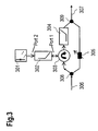
- Fig.3 shows an block diagram of a device that allows for an adjustment of an optical power to provide a substantially constant optical power at its output.
- a Raman tilt control laser (RTCL) 301 is attached to a Port 2 of an optical limiter 302, which has a port Port 1 connected to a circulator 303.
- An optical signal 306 is connected via a coupler 308 to the circulator 303 and to a static attenuator 305.
- the circulator 303 is further connected to a saturable absorber 304. The signal output of said saturable absorber 304 and the signal output by the static attenuator 305 are combined by a coupler 309 into an output signal 307.
- the optical signal 306 cannot directly reach the saturable absorber 304.
- the optical signal 306 is directed via said circulator 303 to the Port 1 of the optical limiter 302 in order to control the control signal provided by the Raman tilt control laser 301 which is then fed back to the circulator 303 and hence to the saturable absorber 304.
- a 2x2-coupler may be used.
- the above exemplary values may result in an substantially constant output signal 307 with an error amounting to less than 10%.
- a Raman tilt determined in dB/THz can be reduced by a factor of more than 10.
- the arrangement described herein may be deployed directly after a photonic cross-connect either at the origin of an optical section or before a first optical amplifier (booster) a the origin of the optical section.
- a photonic cross-connect either at the origin of an optical section or before a first optical amplifier (booster) a the origin of the optical section.
- the approach provided herein allows a utilization of optical limiters for a nominal/actual value comparison and hence to optically control the optical power of an optical light source accordingly.
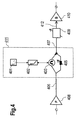
- the arrangement according to Fig.3 may be deployed within a two-stage optical amplifier as depicted in Fig.4 .
- Fig.4 shows an arrangement 411 that is similar to Fig.3 , but without the saturable absorber.
- a Raman tilt control laser 401 provides optical power to a fast optical limiter 402 which is further connected to a circulator 403.
- the circulator 403 conveys an input signal 406 to the limiter 402 and an signal from the limiter 402 towards an output 407.
- the input signal 406 is also fed to the output 407 via an attenuator 405.
- An amplifier 408 with constant gain provides the optical signal 406 and the output signal 408 is conveyed to adjustable slow optical components (ASOC) 409.
- ASOC adjustable slow optical components
- a signal 412 of constant power is fed to a booster 410.
- a gain flattening filter may be provided as a part of the ASOC 409.
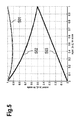
- Fig.5 shows a graph 502 of the power of the Raman tilt control laser 401 as a function of an input signal power 503 in view of the output signal 501 (see signal 407 in Fig.4 ).
- the input signal power can be distributed at a ratio of 2:1, i.e. 2/3 of the total power is used for control power and 1/3 of the total power is used for data signals.
- the input signal 503 varies from a minimum value of 0 (no signal at all) to a maximum value of 1,0.
- an output signal of an amplifier 601 is fed to a band splitter 604 that separates a red portion 602 and a blue portion 603 from the optical signal.
- Each portion 602 and 603 is fed to a separate arrangement 605 and 606 which correspond to the arrangement 411 of Fig.4 .
- the output of each arrangement 605 and 606 is fed to a band-combiner 607 and further conveyed to an adjustable slow optical component ASOC 608.
- the output signal of the ASOC 608 is of constant power and is conveyed to a booster 610.
- Two Raman tilt control lasers are used, each for a subband of the optical transmission band. This allows to sustain not only the Raman tilt but also the Raman gain at a constant level. Furthermore, this approach may be adopted to more than two subbands.
- the embodiment of Fig.6 copes without a saturable absorber. As an option, saturable absorbers may be added according to the embodiment shown in Fig.3 .
- Fig.7A shows a different arrangement that in particular utilizes couplers instead of the circulator shown and explained, e.g., in Fig.3 above.
- a control and signal path comprising a laser 701, a coupler 702, a coupler 703, a limiter 704, a filter 705, an absorber 706 and a coupler 707.
- a signal only path 708 is depicted between the coupler 702 and the coupler 707.
- a signal 710 is input to the coupler 702 and conveyed via said signal path 708 to the coupler 707 that produces an output signal 711.
- the signal 710 is also branched off via said coupler 702 to the coupler 703 to which the laser 701 provides a portion of the optical power of the control signal.
- the coupler 703 conveys the combined signals to the limiter 704. After said limiter 704 the signal is filtered by the filter 705 to reduce the portion of the original signal 710.
- the absorber 706 removes the control offset and provides only the control signal to the coupler 707.
- Fig.7B is similar to the embodiment of Fig.7A .
- the signal path 708 comprises an attenuator 709 to provide a fine adjustment in order to meet or compensate tolerances of the optimizing limiter 704 and absorber 706.
- the output signal 711 comprises a signal portion and a control portion, wherein the power of the output signal 711 is maintained at a constant level.
Landscapes
- Engineering & Computer Science (AREA)
- Computer Networks & Wireless Communication (AREA)
- Signal Processing (AREA)
- Physics & Mathematics (AREA)
- Electromagnetism (AREA)
- Lasers (AREA)
- Optical Communication System (AREA)
- Optical Modulation, Optical Deflection, Nonlinear Optics, Optical Demodulation, Optical Logic Elements (AREA)
Abstract
Description
- The invention relates to a method and to a device for providing and/or controlling an optical signal.
- Groups of optical signals with various wavelengths are transmitted via optical fibers utilizing in particular optical transmission amplifiers.
- In a wavelength division multiplex (WDM) transmission system several data signals (channels) are combined to a channel group. In particular, these channels are amplified together.
- In optical transmission systems, a particular nonlinearity is known as a Raman gain or Raman effect, which is a nonlinear scattering process and results in a power transfer from shorter wavelength channels to longer wavelength channels. The Raman gain becomes significant when a particular level of optical power distributed over a range of wavelengths is pumped into an optical fiber. In such case, the Raman gain is tilted in favor of the channels having the longer wavelengths. This undesired effect is referred to as Raman tilt. This tilt, described in dB/THz, is in a good approximation proportional to the total optical power fed into the fiber. Fast variation of total optical power results in fast variation of Raman induced tilt and constant total optical power results in constant Raman tilt, which can be simply compensated by tilted amplifiers or filters.
- If a transmission is conveyed in a C-band at an overall power amounting to 100mW per amplifier section with channel groups of 80 channels, the so-called Stimulated Raman Scattering (SRS) will result in an attenuation difference amounting of 1dB. If the optical fiber extends to 10-20 amplifier sections, a signal difference in a wavelength range from 1528nm to 1565nm may amount to 10-20dB.
- In optical networks with optical add-drop-multiplexers (OADM), due to adding or dropping channels, the Stimulated Raman Scattering (SRS) has an impact on a level of the channels at the end of the optical fiber and hence at the input of a receiver or amplifier. For example, dropping "red" channels or a breach of fiber may result in the "blue" channels having a level beyond the input range of the amplifier. In addition, the transmission fiber may show an increased degree of nonlinear distortion.
- The problem to be solved is to overcome the disadvantages stated before and in particular to provide an efficient approach to compensate detrimental effects in an optical transmission system by enabling a pure optical solution without any electro-optical converter or electronic control circuitry.
- This problem is solved according to the features of the independent claims. Further embodiments result from the depending claims.
- In order to overcome this problem, a method for providing and/or controlling an optical signal is suggested,
- wherein a control signal and at least one data signal are optically processed into a combined signal of substantially constant optical power,
- wherein the level of the at least one data signal is substantially maintained within the combined signal.
- This approach allows maintaining a constant power level of the combined signal that may be supplied, e.g., at an output of a device or optical circuit arrangement.
- Advantageously, said combined signal is processed by optical means, i.e. without any electro-optical converter or electronic control circuitry.
- In an embodiment, an optical power of the control signal is at least partially supplied by a light source, in particular a laser.
- In another embodiment, at least one wavelength of the light source is disjoint to at least one wavelength utilized for the at least one data signal.
- In particular, the data signal may comprise several channels, wherein wavelengths utilized for the data signal are in particular disjoint from the wavelength used by the light source.
- In a further embodiment, the light source comprises a Raman tilt control laser.
- In a next embodiment, the optical signal of the light source and the at least one data signal are fed to an optical limiter in order to obtain the combined signal.
- The optical limiter processes the signals provided in particular by limiting an output power to a predefined threshold "lim". Below such threshold value the input power may substantially equal the output power of the limiter.
- It is also an embodiment that the optical signal of the light source and the at least one data signal are fed to the optical limiter via a circulator or via a coupler.
- Pursuant to another embodiment, the optical limiter comprises a semiconductor optical amplifier (SOA).
- According to an embodiment, an output of the optical limiter is processed by an absorber and then combined with the data signal into said combined signal. Preferably, a filter may process the input signal of the absorber, wherein said filter may advantageously have a substantially inverse characteristics of the absorber.
- The absorber may in particular be a saturable absorber.
- According to another embodiment, the absorber comprises a semiconductor optical amplifier (SOA) or an erbium doped fiber amplifier (EDFA).
- The EDFA in an absorber may in particular be used to adjust a threshold of its limiting power.
- In yet another embodiment, the control signal compensates at least partially a Raman tilt and/or a Raman gain.
- The problem stated above is also solved by a device for controlling an optical signal comprising
- a light source, in particular at least one laser, to at least partially provide an optical power of a control signal;
- a limiter fed by the signal from the light source and by a data signal providing an combined signal of substantially constant optical power.
- According to an embodiment, the data signal is coupled with the output of the limiter to provide said combined signal.
- According to a next embodiment, the data signal is coupled via an attenuator, in particular via an adjustable attenuator, with the output of the limiter to provide said combined signal.
- Pursuant to yet an embodiment, the output of the limiter is fed to an absorber, wherein the output of said absorber provides (an optical power of) a control signal portion of the combined signal.
- As a next embodiment, a filter is provided before the absorber, wherein said filter in particular shows a substantially inverse characteristics of the absorber.
- It is also an embodiment that a circulator is provided to combine the data signal and the signal from the light source.
- As an alternative embodiment, a coupler may be provided to combine the data signal and the signal from the light source.
- Pursuant to an embodiment, the device may be used in or part of an optical transmission system, said system comprising at least one semiconductor optical amplifier (SOA) for suppressing and/or reducing noise and/or interference by cross gain modulation.
Furthermore, such device may comprise at least one switch that is based on or realized by at least one semiconductor optical amplifier (SOA). - Embodiments of the invention are shown and illustrated in the following figures:
- Fig.1
- shows a transfer characteristics of an erbium 3+ doped glass fiber;
- Fig.2
- shows a quadripole of a limiter comprising two ports;
- Fig.3
- shows a block diagram of a power control device that allows adjustment of an optical power to provide a substantially constant optical power at its output;
- Fig.4
- shows a block diagram of an optical power control device deployed within a two-stage optical amplifier;
- Fig.5
- shows a graph of the power of the Raman tilt control laser as a function of an input signal power in view of an output signal;
- Fig.6
- shows a block diagram of an optical power control device for two different subbands;
- Fig.7A
- shows an optical total power control unit with a first path comprising an optical data signal and a control information and a second path comprising the optical data signal only, wherein a laser pumps external optical power to the first path to provide a control signal;
- Fig.7B
- shows the optical total power control unit of
Fig.7A with an attenuator arranged in the second path. - A semiconductor optical amplifier (SOA) is described in [1]. Such SOA may be utilized as a saturable absorber or as a limiter. Furthermore, an erbium doped fiber amplifier (EDFA) can be used in addition or instead.
- The approach provided herein suggests an optical solution for a fast control of an optical signal without additional electro-optical converters or additional electronic control circuits.
- A transparency T of an ideal optical limiter with a limiting power "lim" can be denoted as follows:

with
and
wherein P refers to a power of the optical signal.
results to
and
- In addition, a saturable absorber can be denoted as


- Advantageously, the limiter and/or the absorber are used in order to provide an arrangement with a constant optical output power even if single data signals are dropped:

with Pdata being a power of a data signal comprising several single data signals P λk with k=1,..,n, n being a number of channels of the optical band to be controlled, and Pcontrol being a power of a control signal. - In addition, if at least one data signal is dropped, the remaining data signals sustain their respective power level.
- The requirement set forth by equation (3) can be met by providing at least two signal paths:
- (a) A control path for adjusting the control signal and
- (b) a data path to which the adjusted control signal is added.
- The wavelength utilized by a control laser supplying the optical power to the control path is disjoint to the wavelengths of the data signals (channels).
- The saturable absorber subtracts a constant amount of light power from the signal and may hence be utilized to remove a constant offset from the signal. This is in particular useful to remove an offset of a control laser that is set to full level.
- Embodiments without such saturable absorber will be referred to in more detail below.
- An absorber may in particular be realized by an erbium doped (Er3+) glass fiber allowing for a time delay in a range of 100s of milliseconds. A transfer characteristics of a typically doped glass fiber used as saturable absorber is shown in
Fig.1 . - It is to be noted that such an erbium doped glass fiber may require a filter put in front of the absorber comprising an inverse characteristics of the saturable absorber.
- The approach presented advantageously exploits the fact that the transmission characteristics of the optical limiter depends on the input power of the optical signal as follows:


-
Fig.2 shows the corresponding quadripole of the limiter. However, the indices in equations (4.1) and (4.2) may refer to different directions of a signal or to different wavelengths. - It may in particular be extraneous whether the optical signals towards or from the limiter are co-directional or contra-directional. The limiter may be realized in order to work properly independent from particular wavelengths applied.
- Equations (4.1) and (4.2) correspond to a
term 
that can be expanded into a series as follows:
- For x<0,3 an error for discontinuing the series after the linear term is below 10%.
-
Fig.3 shows an block diagram of a device that allows for an adjustment of an optical power to provide a substantially constant optical power at its output. - A Raman tilt control laser (RTCL) 301 is attached to a
Port 2 of anoptical limiter 302, which has aport Port 1 connected to acirculator 303. Anoptical signal 306 is connected via acoupler 308 to thecirculator 303 and to astatic attenuator 305. Thecirculator 303 is further connected to a saturable absorber 304.The signal output of saidsaturable absorber 304 and the signal output by thestatic attenuator 305 are combined by acoupler 309 into anoutput signal 307. - According to the
circulator 303, theoptical signal 306 cannot directly reach thesaturable absorber 304. Theoptical signal 306 is directed via saidcirculator 303 to thePort 1 of theoptical limiter 302 in order to control the control signal provided by the Ramantilt control laser 301 which is then fed back to thecirculator 303 and hence to thesaturable absorber 304. - As an alternative for the
circulator 303, a 2x2-coupler may be used. - As an example, an optical signal Pcontrol2 provided by the Raman
tilt control laser 301 and input to thePort 2 of theoptical limiter 302 may amount to
via a 50:50 coupler;
and
with P 306 being the power of theoptical input signal 306. The above exemplary values may result in an substantiallyconstant output signal 307 with an error amounting to less than 10%. Hence, a Raman tilt determined in dB/THz can be reduced by a factor of more than 10. - The arrangement described herein may be deployed directly after a photonic cross-connect either at the origin of an optical section or before a first optical amplifier (booster) a the origin of the optical section.
- Advantageously, the approach provided herein allows a utilization of optical limiters for a nominal/actual value comparison and hence to optically control the optical power of an optical light source accordingly.
- The arrangement according to
Fig.3 may be deployed within a two-stage optical amplifier as depicted inFig.4 . -
Fig.4 shows anarrangement 411 that is similar toFig.3 , but without the saturable absorber. - Hence, a Raman
tilt control laser 401 provides optical power to a fastoptical limiter 402 which is further connected to acirculator 403. Thecirculator 403 conveys aninput signal 406 to thelimiter 402 and an signal from thelimiter 402 towards anoutput 407. Theinput signal 406 is also fed to theoutput 407 via anattenuator 405. - An
amplifier 408 with constant gain provides theoptical signal 406 and theoutput signal 408 is conveyed to adjustable slow optical components (ASOC) 409. Asignal 412 of constant power is fed to abooster 410. In particular, a gain flattening filter may be provided as a part of theASOC 409. -
Fig.5 shows agraph 502 of the power of the Ramantilt control laser 401 as a function of aninput signal power 503 in view of the output signal 501 (seesignal 407 inFig.4 ). - According to
Fig.5 , the input signal power can be distributed at a ratio of 2:1, i.e. 2/3 of the total power is used for control power and 1/3 of the total power is used for data signals. Theinput signal 503 varies from a minimum value of 0 (no signal at all) to a maximum value of 1,0. - In an example shown in
Fig.6 , an output signal of anamplifier 601 is fed to aband splitter 604 that separates ared portion 602 and ablue portion 603 from the optical signal. Eachportion separate arrangement arrangement 411 ofFig.4 . The output of eacharrangement combiner 607 and further conveyed to an adjustable slowoptical component ASOC 608. The output signal of theASOC 608 is of constant power and is conveyed to abooster 610. - Two Raman tilt control lasers are used, each for a subband of the optical transmission band. This allows to sustain not only the Raman tilt but also the Raman gain at a constant level. Furthermore, this approach may be adopted to more than two subbands. The embodiment of
Fig.6 copes without a saturable absorber. As an option, saturable absorbers may be added according to the embodiment shown inFig.3 . - It is in particular possible to provide a more complex arrangement comprising more parallel control paths and hence to obtain the same precision but without providing any saturable absorber.
-
Fig.7A shows a different arrangement that in particular utilizes couplers instead of the circulator shown and explained, e.g., inFig.3 above. - In
Fig.7A , a control and signal path is depicted comprising alaser 701, acoupler 702, acoupler 703, alimiter 704, afilter 705, anabsorber 706 and acoupler 707. In addition, a signalonly path 708 is depicted between thecoupler 702 and thecoupler 707. - A
signal 710 is input to thecoupler 702 and conveyed via saidsignal path 708 to thecoupler 707 that produces anoutput signal 711. - In addition, the
signal 710 is also branched off via saidcoupler 702 to thecoupler 703 to which thelaser 701 provides a portion of the optical power of the control signal. Thecoupler 703 conveys the combined signals to thelimiter 704. After saidlimiter 704 the signal is filtered by thefilter 705 to reduce the portion of theoriginal signal 710. Theabsorber 706 removes the control offset and provides only the control signal to thecoupler 707. -
Fig.7B is similar to the embodiment ofFig.7A . The only difference is that thesignal path 708 comprises anattenuator 709 to provide a fine adjustment in order to meet or compensate tolerances of the optimizinglimiter 704 andabsorber 706. - The
output signal 711 comprises a signal portion and a control portion, wherein the power of theoutput signal 711 is maintained at a constant level. -
- [1] ROPP C, GOLDHAR J: "Nonlinear Mach-Zehnder Interferometer as a DPSK Signal Regenerator", http://www.ece.umd.edu/merit/archives/merit2006/merit _fair06_papers/Paper_11_Ropp.pdf
Claims (22)
- A method for providing and/or controlling an optical signal,- wherein a control signal and at least one data signal are optically processed into a combined signal of substantially constant optical power,- wherein the level of the at least one data signal is substantially maintained within the combined signal.
- The method according to claim 1, wherein an optical power of the control signal is at least partially supplied by a light source, in particular a laser.
- The method according to claim 2, wherein at least one wavelength of the light source is disjoint to at least one wavelength utilized for the at least one data signal.
- The method according to any of claims 2 or 3, wherein the light source comprises a Raman tilt control laser.
- The method according to any of claims 2 to 4, wherein the optical signal of the light source and the at least one data signal are fed to an optical limiter in order to obtain the combined signal.
- The method according to claim 5, wherein the optical signal of the light source and the at least one data signal are fed to the optical limiter via a circulator or via a coupler.
- The method according to any of claims 5 or 6, wherein the optical limiter comprises a semiconductor optical amplifier (SOA).
- The method according to any of claims 5 to 7, wherein an output of the optical limiter is processed by an absorber and then combined with the data signal into said combined signal.
- The method according to claim 8, wherein a filter processes the input signal of the absorber.
- The method according to claim 9, wherein said filter has a substantially inverse characteristics of the absorber.
- The method according to any of claims 8 to 10, wherein the absorber is a saturable absorber.
- The method according to any of claims 8 to 11, wherein the absorber comprises a semiconductor optical amplifier (SOA) or an erbium doped fiber amplifier (EDFA).
- The method according to any of the preceding claims, wherein the control signal compensates at least partially a Raman tilt and/or a Raman gain.
- A device for providing and/or controlling an optical signal comprising- a light source, in particular at least one laser, to at least partially provide an optical power of a control signal;- a limiter fed by the signal from the light source and by a data signal providing an combined signal of substantially constant optical power.
- The device according to claim 14, wherein the data signal is coupled with the output of the limiter to provide said combined signal.
- The device according to claim 14, wherein the data signal is coupled via an attenuator, in particular via an adjustable attenuator, with the output of the limiter to provide said combined signal.
- The device according to any of claims 14 to 16, wherein the output of the limiter is fed to an absorber, wherein the output of said absorber provides a control signal portion of the combined signal.
- The device according to claim 17, wherein a filter is provided before the absorber, wherein said filter in particular shows a substantially inverse characteristics of the absorber.
- The device according to any of claims 14 to 18, wherein a circulator is provided to combine the data signal and the signal from the light source.
- The device according to any of claims 14 to 19, wherein a coupler is provided to combine the data signal and the signal from the light source.
- The device according to any of claims 14 to 20 used in an optical transmission system, said transmission system comprising at least one semiconductor optical amplifier for suppressing and/or reducing noise and/or interference by cross gain modulation.
- The device according to claim 21 comprising at least one switch that is based on at least one semiconductor optical amplifier.
Priority Applications (3)
| Application Number | Priority Date | Filing Date | Title |
|---|---|---|---|
| EP08000698.4A EP2081308B1 (en) | 2008-01-15 | 2008-01-15 | Method and device for providing and/or controlling an optical signal |
| US12/812,997 US8462428B2 (en) | 2008-01-15 | 2009-01-12 | Method and device for providing and/or controlling an optical signal |
| PCT/EP2009/050242 WO2009090144A1 (en) | 2008-01-15 | 2009-01-12 | Method and device for providing and/or controlling an optical signal |
Applications Claiming Priority (1)
| Application Number | Priority Date | Filing Date | Title |
|---|---|---|---|
| EP08000698.4A EP2081308B1 (en) | 2008-01-15 | 2008-01-15 | Method and device for providing and/or controlling an optical signal |
Publications (2)
| Publication Number | Publication Date |
|---|---|
| EP2081308A1 true EP2081308A1 (en) | 2009-07-22 |
| EP2081308B1 EP2081308B1 (en) | 2013-08-28 |
Family
ID=39485139
Family Applications (1)
| Application Number | Title | Priority Date | Filing Date |
|---|---|---|---|
| EP08000698.4A Active EP2081308B1 (en) | 2008-01-15 | 2008-01-15 | Method and device for providing and/or controlling an optical signal |
Country Status (3)
| Country | Link |
|---|---|
| US (1) | US8462428B2 (en) |
| EP (1) | EP2081308B1 (en) |
| WO (1) | WO2009090144A1 (en) |
Families Citing this family (1)
| Publication number | Priority date | Publication date | Assignee | Title |
|---|---|---|---|---|
| EP3641162A4 (en) | 2017-05-27 | 2020-05-20 | Huawei Technologies Co. Ltd. | Method and device for compensating optical power |
Citations (7)
| Publication number | Priority date | Publication date | Assignee | Title |
|---|---|---|---|---|
| EP0829981A2 (en) | 1996-09-13 | 1998-03-18 | Lucent Technologies Inc. | System and method for mitigating cross-saturation in optically amplified networks |
| US5900968A (en) | 1996-02-23 | 1999-05-04 | Lucent Technologies Inc. | Method of fast gain control in WDM optical networks |
| US6785042B1 (en) | 1999-04-23 | 2004-08-31 | Fujitsu Limited | Slope control of gain wavelength of raman amplification |
| US20060044657A1 (en) | 2004-08-11 | 2006-03-02 | Siemens Aktiengesellschaft | Method and arrangement for the rapid adjustment of the tilt of optical WDM signals |
| US7024117B1 (en) | 1997-11-28 | 2006-04-04 | Siémens Aktiengesellschaft | Method and apparatus for adjusting tilting and level of optical signals |
| US20060177221A1 (en) | 2003-01-28 | 2006-08-10 | Marconi Communitions Gmbh | Transmitter and method for transmitting messages on an optical fiber |
| US20060263089A1 (en) | 2003-01-28 | 2006-11-23 | Cornelius Furst | Output stage for carrying out wdm message transmission and methods for exchanging full light sources in an output stage of this type |
Family Cites Families (2)
| Publication number | Priority date | Publication date | Assignee | Title |
|---|---|---|---|---|
| JP2006066610A (en) * | 2004-08-26 | 2006-03-09 | Fujitsu Ltd | Optical amplifier, Raman amplifier, optical wavelength division multiplexing transmission system, optical wavelength division multiplexing transmission method |
| US7362448B1 (en) * | 2004-09-08 | 2008-04-22 | Nanometrics Incorporated | Characterizing residue on a sample |
-
2008
- 2008-01-15 EP EP08000698.4A patent/EP2081308B1/en active Active
-
2009
- 2009-01-12 US US12/812,997 patent/US8462428B2/en active Active
- 2009-01-12 WO PCT/EP2009/050242 patent/WO2009090144A1/en not_active Ceased
Patent Citations (7)
| Publication number | Priority date | Publication date | Assignee | Title |
|---|---|---|---|---|
| US5900968A (en) | 1996-02-23 | 1999-05-04 | Lucent Technologies Inc. | Method of fast gain control in WDM optical networks |
| EP0829981A2 (en) | 1996-09-13 | 1998-03-18 | Lucent Technologies Inc. | System and method for mitigating cross-saturation in optically amplified networks |
| US7024117B1 (en) | 1997-11-28 | 2006-04-04 | Siémens Aktiengesellschaft | Method and apparatus for adjusting tilting and level of optical signals |
| US6785042B1 (en) | 1999-04-23 | 2004-08-31 | Fujitsu Limited | Slope control of gain wavelength of raman amplification |
| US20060177221A1 (en) | 2003-01-28 | 2006-08-10 | Marconi Communitions Gmbh | Transmitter and method for transmitting messages on an optical fiber |
| US20060263089A1 (en) | 2003-01-28 | 2006-11-23 | Cornelius Furst | Output stage for carrying out wdm message transmission and methods for exchanging full light sources in an output stage of this type |
| US20060044657A1 (en) | 2004-08-11 | 2006-03-02 | Siemens Aktiengesellschaft | Method and arrangement for the rapid adjustment of the tilt of optical WDM signals |
Also Published As
| Publication number | Publication date |
|---|---|
| US8462428B2 (en) | 2013-06-11 |
| US20110051228A1 (en) | 2011-03-03 |
| WO2009090144A1 (en) | 2009-07-23 |
| EP2081308B1 (en) | 2013-08-28 |
Similar Documents
| Publication | Publication Date | Title |
|---|---|---|
| EP1381125B1 (en) | Method and device for optical amplification and system having the device | |
| US6310716B1 (en) | Amplifier system with a discrete Raman fiber amplifier module | |
| CA2335289C (en) | Fiber-optic compensation for dispersion, gain tilt, and band pump nonlinearity | |
| JP3527671B2 (en) | Method of controlling wavelength characteristics of optical transmission power by Raman amplification, wavelength division multiplexing optical communication system and optical amplifier using the same | |
| US7200333B2 (en) | Optical communication apparatus, system, and method that properly compensate for chromatic dispersion | |
| EP1013021B1 (en) | Dynamic optical amplifier | |
| EP1248392B1 (en) | Optical amplifier device and bidirectional wavelength division multiplexing optical communication system using the same | |
| JP2734969B2 (en) | Optical fiber amplifier for WDM transmission | |
| JPH0697890A (en) | Optical transmission equipment | |
| JP3769129B2 (en) | Optical amplifier and optical communication system having chromatic dispersion compensation function | |
| CA2409251A1 (en) | Broadband amplifier and communication system | |
| WO2002058198A2 (en) | Broadband optical amplifier | |
| JPH09244079A (en) | Gain equalizer and optical transmission system | |
| JPH10276172A (en) | Wavelength division optical processing device and optical communication transmission line using this wavelength division optical processing device | |
| US6671083B2 (en) | Raman amplifier and optical transmission system | |
| KR100421136B1 (en) | Wide band erbium doped fiber amplifier and wavelength division multiplexing transmission system therewith | |
| US6823107B2 (en) | Method and device for optical amplification | |
| JPH11204866A (en) | Wavelength multiplexing signal amplification repeater and optical communication transmission line using the repeater | |
| JP2006066862A (en) | Wavelength multiplexed signal light amplification method and optical amplifier | |
| JP7063329B2 (en) | Optical repeater, control method of optical repeater, and optical transmission system | |
| US8462428B2 (en) | Method and device for providing and/or controlling an optical signal | |
| US20050286119A1 (en) | Article comprising a wideband optical amplifier with a wide dynamic range | |
| US6829407B2 (en) | Planar optical circuit and optical transmission system | |
| JP3609968B2 (en) | Optical amplifier | |
| JPH1146167A (en) | Optical repeater |
Legal Events
| Date | Code | Title | Description |
|---|---|---|---|
| PUAI | Public reference made under article 153(3) epc to a published international application that has entered the european phase |
Free format text: ORIGINAL CODE: 0009012 |
|
| AK | Designated contracting states |
Kind code of ref document: A1 Designated state(s): AT BE BG CH CY CZ DE DK EE ES FI FR GB GR HR HU IE IS IT LI LT LU LV MC MT NL NO PL PT RO SE SI SK TR |
|
| AX | Request for extension of the european patent |
Extension state: AL BA MK RS |
|
| 17P | Request for examination filed |
Effective date: 20100122 |
|
| 17Q | First examination report despatched |
Effective date: 20100216 |
|
| AKX | Designation fees paid |
Designated state(s): AT BE BG CH CY CZ DE DK EE ES FI FR GB GR HR HU IE IS IT LI LT LU LV MC MT NL NO PL PT RO SE SI SK TR |
|
| RAP1 | Party data changed (applicant data changed or rights of an application transferred) |
Owner name: NOKIA SIEMENS NETWORKS GMBH & CO. KG |
|
| REG | Reference to a national code |
Ref country code: DE Ref legal event code: R079 Ref document number: 602008027107 Country of ref document: DE Free format text: PREVIOUS MAIN CLASS: H04B0010180000 Ipc: H04B0010296000 |
|
| RIC1 | Information provided on ipc code assigned before grant |
Ipc: H04B 10/2537 20130101ALI20130131BHEP Ipc: H04B 10/296 20130101AFI20130131BHEP |
|
| GRAP | Despatch of communication of intention to grant a patent |
Free format text: ORIGINAL CODE: EPIDOSNIGR1 |
|
| GRAS | Grant fee paid |
Free format text: ORIGINAL CODE: EPIDOSNIGR3 |
|
| GRAA | (expected) grant |
Free format text: ORIGINAL CODE: 0009210 |
|
| AK | Designated contracting states |
Kind code of ref document: B1 Designated state(s): AT BE BG CH CY CZ DE DK EE ES FI FR GB GR HR HU IE IS IT LI LT LU LV MC MT NL NO PL PT RO SE SI SK TR |
|
| REG | Reference to a national code |
Ref country code: GB Ref legal event code: FG4D |
|
| REG | Reference to a national code |
Ref country code: CH Ref legal event code: EP |
|
| REG | Reference to a national code |
Ref country code: AT Ref legal event code: REF Ref document number: 629827 Country of ref document: AT Kind code of ref document: T Effective date: 20130915 |
|
| REG | Reference to a national code |
Ref country code: IE Ref legal event code: FG4D |
|
| REG | Reference to a national code |
Ref country code: DE Ref legal event code: R096 Ref document number: 602008027107 Country of ref document: DE Effective date: 20131024 |
|
| RAP2 | Party data changed (patent owner data changed or rights of a patent transferred) |
Owner name: NOKIA SOLUTIONS AND NETWORKS GMBH & CO. KG |
|
| RAP2 | Party data changed (patent owner data changed or rights of a patent transferred) |
Owner name: XIEON NETWORKS S.A.R.L. |
|
| REG | Reference to a national code |
Ref country code: AT Ref legal event code: MK05 Ref document number: 629827 Country of ref document: AT Kind code of ref document: T Effective date: 20130828 |
|
| REG | Reference to a national code |
Ref country code: DE Ref legal event code: R081 Ref document number: 602008027107 Country of ref document: DE Owner name: XIEON NETWORKS S.A.R.L., LU Free format text: FORMER OWNER: NOKIA SIEMENS NETWORKS GMBH & CO. KG, 81541 MUENCHEN, DE Effective date: 20131121 Ref country code: DE Ref legal event code: R082 Ref document number: 602008027107 Country of ref document: DE Representative=s name: BOEHMERT & BOEHMERT ANWALTSPARTNERSCHAFT MBB -, DE Effective date: 20131121 Ref country code: DE Ref legal event code: R082 Ref document number: 602008027107 Country of ref document: DE Representative=s name: BOEHMERT & BOEHMERT, DE Effective date: 20131121 |
|
| REG | Reference to a national code |
Ref country code: LT Ref legal event code: MG4D |
|
| REG | Reference to a national code |
Ref country code: NL Ref legal event code: VDEP Effective date: 20130828 |
|
| PG25 | Lapsed in a contracting state [announced via postgrant information from national office to epo] |
Ref country code: AT Free format text: LAPSE BECAUSE OF FAILURE TO SUBMIT A TRANSLATION OF THE DESCRIPTION OR TO PAY THE FEE WITHIN THE PRESCRIBED TIME-LIMIT Effective date: 20130828 Ref country code: HR Free format text: LAPSE BECAUSE OF FAILURE TO SUBMIT A TRANSLATION OF THE DESCRIPTION OR TO PAY THE FEE WITHIN THE PRESCRIBED TIME-LIMIT Effective date: 20130828 Ref country code: SE Free format text: LAPSE BECAUSE OF FAILURE TO SUBMIT A TRANSLATION OF THE DESCRIPTION OR TO PAY THE FEE WITHIN THE PRESCRIBED TIME-LIMIT Effective date: 20130828 Ref country code: LT Free format text: LAPSE BECAUSE OF FAILURE TO SUBMIT A TRANSLATION OF THE DESCRIPTION OR TO PAY THE FEE WITHIN THE PRESCRIBED TIME-LIMIT Effective date: 20130828 Ref country code: NO Free format text: LAPSE BECAUSE OF FAILURE TO SUBMIT A TRANSLATION OF THE DESCRIPTION OR TO PAY THE FEE WITHIN THE PRESCRIBED TIME-LIMIT Effective date: 20131128 Ref country code: CY Free format text: LAPSE BECAUSE OF FAILURE TO SUBMIT A TRANSLATION OF THE DESCRIPTION OR TO PAY THE FEE WITHIN THE PRESCRIBED TIME-LIMIT Effective date: 20130731 Ref country code: PT Free format text: LAPSE BECAUSE OF FAILURE TO SUBMIT A TRANSLATION OF THE DESCRIPTION OR TO PAY THE FEE WITHIN THE PRESCRIBED TIME-LIMIT Effective date: 20131230 Ref country code: IS Free format text: LAPSE BECAUSE OF FAILURE TO SUBMIT A TRANSLATION OF THE DESCRIPTION OR TO PAY THE FEE WITHIN THE PRESCRIBED TIME-LIMIT Effective date: 20131228 |
|
| REG | Reference to a national code |
Ref country code: NL Ref legal event code: VDEP Effective date: 20130828 |
|
| REG | Reference to a national code |
Ref country code: GB Ref legal event code: 732E Free format text: REGISTERED BETWEEN 20140130 AND 20140205 |
|
| PG25 | Lapsed in a contracting state [announced via postgrant information from national office to epo] |
Ref country code: FI Free format text: LAPSE BECAUSE OF FAILURE TO SUBMIT A TRANSLATION OF THE DESCRIPTION OR TO PAY THE FEE WITHIN THE PRESCRIBED TIME-LIMIT Effective date: 20130828 Ref country code: LV Free format text: LAPSE BECAUSE OF FAILURE TO SUBMIT A TRANSLATION OF THE DESCRIPTION OR TO PAY THE FEE WITHIN THE PRESCRIBED TIME-LIMIT Effective date: 20130828 Ref country code: GR Free format text: LAPSE BECAUSE OF FAILURE TO SUBMIT A TRANSLATION OF THE DESCRIPTION OR TO PAY THE FEE WITHIN THE PRESCRIBED TIME-LIMIT Effective date: 20131129 Ref country code: BE Free format text: LAPSE BECAUSE OF FAILURE TO SUBMIT A TRANSLATION OF THE DESCRIPTION OR TO PAY THE FEE WITHIN THE PRESCRIBED TIME-LIMIT Effective date: 20130828 Ref country code: SI Free format text: LAPSE BECAUSE OF FAILURE TO SUBMIT A TRANSLATION OF THE DESCRIPTION OR TO PAY THE FEE WITHIN THE PRESCRIBED TIME-LIMIT Effective date: 20130828 Ref country code: PL Free format text: LAPSE BECAUSE OF FAILURE TO SUBMIT A TRANSLATION OF THE DESCRIPTION OR TO PAY THE FEE WITHIN THE PRESCRIBED TIME-LIMIT Effective date: 20130828 |
|
| PG25 | Lapsed in a contracting state [announced via postgrant information from national office to epo] |
Ref country code: CY Free format text: LAPSE BECAUSE OF FAILURE TO SUBMIT A TRANSLATION OF THE DESCRIPTION OR TO PAY THE FEE WITHIN THE PRESCRIBED TIME-LIMIT Effective date: 20130828 |
|
| PG25 | Lapsed in a contracting state [announced via postgrant information from national office to epo] |
Ref country code: CZ Free format text: LAPSE BECAUSE OF FAILURE TO SUBMIT A TRANSLATION OF THE DESCRIPTION OR TO PAY THE FEE WITHIN THE PRESCRIBED TIME-LIMIT Effective date: 20130828 Ref country code: NL Free format text: LAPSE BECAUSE OF FAILURE TO SUBMIT A TRANSLATION OF THE DESCRIPTION OR TO PAY THE FEE WITHIN THE PRESCRIBED TIME-LIMIT Effective date: 20130828 Ref country code: EE Free format text: LAPSE BECAUSE OF FAILURE TO SUBMIT A TRANSLATION OF THE DESCRIPTION OR TO PAY THE FEE WITHIN THE PRESCRIBED TIME-LIMIT Effective date: 20130828 Ref country code: DK Free format text: LAPSE BECAUSE OF FAILURE TO SUBMIT A TRANSLATION OF THE DESCRIPTION OR TO PAY THE FEE WITHIN THE PRESCRIBED TIME-LIMIT Effective date: 20130828 Ref country code: RO Free format text: LAPSE BECAUSE OF FAILURE TO SUBMIT A TRANSLATION OF THE DESCRIPTION OR TO PAY THE FEE WITHIN THE PRESCRIBED TIME-LIMIT Effective date: 20130828 Ref country code: SK Free format text: LAPSE BECAUSE OF FAILURE TO SUBMIT A TRANSLATION OF THE DESCRIPTION OR TO PAY THE FEE WITHIN THE PRESCRIBED TIME-LIMIT Effective date: 20130828 |
|
| REG | Reference to a national code |
Ref country code: FR Ref legal event code: GC Effective date: 20140408 |
|
| PG25 | Lapsed in a contracting state [announced via postgrant information from national office to epo] |
Ref country code: ES Free format text: LAPSE BECAUSE OF FAILURE TO SUBMIT A TRANSLATION OF THE DESCRIPTION OR TO PAY THE FEE WITHIN THE PRESCRIBED TIME-LIMIT Effective date: 20130828 Ref country code: IT Free format text: LAPSE BECAUSE OF FAILURE TO SUBMIT A TRANSLATION OF THE DESCRIPTION OR TO PAY THE FEE WITHIN THE PRESCRIBED TIME-LIMIT Effective date: 20130828 |
|
| REG | Reference to a national code |
Ref country code: DE Ref legal event code: R097 Ref document number: 602008027107 Country of ref document: DE |
|
| PLBE | No opposition filed within time limit |
Free format text: ORIGINAL CODE: 0009261 |
|
| STAA | Information on the status of an ep patent application or granted ep patent |
Free format text: STATUS: NO OPPOSITION FILED WITHIN TIME LIMIT |
|
| 26N | No opposition filed |
Effective date: 20140530 |
|
| PG25 | Lapsed in a contracting state [announced via postgrant information from national office to epo] |
Ref country code: LU Free format text: LAPSE BECAUSE OF FAILURE TO SUBMIT A TRANSLATION OF THE DESCRIPTION OR TO PAY THE FEE WITHIN THE PRESCRIBED TIME-LIMIT Effective date: 20140115 Ref country code: MC Free format text: LAPSE BECAUSE OF FAILURE TO SUBMIT A TRANSLATION OF THE DESCRIPTION OR TO PAY THE FEE WITHIN THE PRESCRIBED TIME-LIMIT Effective date: 20130828 |
|
| REG | Reference to a national code |
Ref country code: CH Ref legal event code: PL |
|
| REG | Reference to a national code |
Ref country code: DE Ref legal event code: R097 Ref document number: 602008027107 Country of ref document: DE Effective date: 20140530 |
|
| PG25 | Lapsed in a contracting state [announced via postgrant information from national office to epo] |
Ref country code: LI Free format text: LAPSE BECAUSE OF NON-PAYMENT OF DUE FEES Effective date: 20140131 Ref country code: CH Free format text: LAPSE BECAUSE OF NON-PAYMENT OF DUE FEES Effective date: 20140131 |
|
| REG | Reference to a national code |
Ref country code: IE Ref legal event code: MM4A |
|
| PG25 | Lapsed in a contracting state [announced via postgrant information from national office to epo] |
Ref country code: IE Free format text: LAPSE BECAUSE OF NON-PAYMENT OF DUE FEES Effective date: 20140115 |
|
| REG | Reference to a national code |
Ref country code: FR Ref legal event code: GC Effective date: 20150922 |
|
| REG | Reference to a national code |
Ref country code: FR Ref legal event code: PLFP Year of fee payment: 9 |
|
| PG25 | Lapsed in a contracting state [announced via postgrant information from national office to epo] |
Ref country code: MT Free format text: LAPSE BECAUSE OF FAILURE TO SUBMIT A TRANSLATION OF THE DESCRIPTION OR TO PAY THE FEE WITHIN THE PRESCRIBED TIME-LIMIT Effective date: 20130828 |
|
| PG25 | Lapsed in a contracting state [announced via postgrant information from national office to epo] |
Ref country code: BG Free format text: LAPSE BECAUSE OF FAILURE TO SUBMIT A TRANSLATION OF THE DESCRIPTION OR TO PAY THE FEE WITHIN THE PRESCRIBED TIME-LIMIT Effective date: 20130828 |
|
| PGFP | Annual fee paid to national office [announced via postgrant information from national office to epo] |
Ref country code: GB Payment date: 20160120 Year of fee payment: 9 Ref country code: FR Payment date: 20160121 Year of fee payment: 9 |
|
| PG25 | Lapsed in a contracting state [announced via postgrant information from national office to epo] |
Ref country code: TR Free format text: LAPSE BECAUSE OF FAILURE TO SUBMIT A TRANSLATION OF THE DESCRIPTION OR TO PAY THE FEE WITHIN THE PRESCRIBED TIME-LIMIT Effective date: 20130828 Ref country code: HU Free format text: LAPSE BECAUSE OF FAILURE TO SUBMIT A TRANSLATION OF THE DESCRIPTION OR TO PAY THE FEE WITHIN THE PRESCRIBED TIME-LIMIT; INVALID AB INITIO Effective date: 20080115 |
|
| GBPC | Gb: european patent ceased through non-payment of renewal fee |
Effective date: 20170115 |
|
| REG | Reference to a national code |
Ref country code: FR Ref legal event code: ST Effective date: 20170929 |
|
| PG25 | Lapsed in a contracting state [announced via postgrant information from national office to epo] |
Ref country code: FR Free format text: LAPSE BECAUSE OF NON-PAYMENT OF DUE FEES Effective date: 20170131 |
|
| PG25 | Lapsed in a contracting state [announced via postgrant information from national office to epo] |
Ref country code: GB Free format text: LAPSE BECAUSE OF NON-PAYMENT OF DUE FEES Effective date: 20170115 |
|
| PGFP | Annual fee paid to national office [announced via postgrant information from national office to epo] |
Ref country code: DE Payment date: 20251203 Year of fee payment: 19 |