EP2080221B1 - A susceptor and method of forming a led device using such susceptor - Google Patents
A susceptor and method of forming a led device using such susceptor Download PDFInfo
- Publication number
- EP2080221B1 EP2080221B1 EP07868710A EP07868710A EP2080221B1 EP 2080221 B1 EP2080221 B1 EP 2080221B1 EP 07868710 A EP07868710 A EP 07868710A EP 07868710 A EP07868710 A EP 07868710A EP 2080221 B1 EP2080221 B1 EP 2080221B1
- Authority
- EP
- European Patent Office
- Prior art keywords
- susceptor
- layer
- semiconductor layer
- silicon
- recess
- Prior art date
- Legal status (The legal status is an assumption and is not a legal conclusion. Google has not performed a legal analysis and makes no representation as to the accuracy of the status listed.)
- Not-in-force
Links
Images


Classifications
-
- H—ELECTRICITY
- H01—ELECTRIC ELEMENTS
- H01L—SEMICONDUCTOR DEVICES NOT COVERED BY CLASS H10
- H01L21/00—Processes or apparatus adapted for the manufacture or treatment of semiconductor or solid state devices or of parts thereof
- H01L21/67—Apparatus specially adapted for handling semiconductor or electric solid state devices during manufacture or treatment thereof; Apparatus specially adapted for handling wafers during manufacture or treatment of semiconductor or electric solid state devices or components ; Apparatus not specifically provided for elsewhere
- H01L21/683—Apparatus specially adapted for handling semiconductor or electric solid state devices during manufacture or treatment thereof; Apparatus specially adapted for handling wafers during manufacture or treatment of semiconductor or electric solid state devices or components ; Apparatus not specifically provided for elsewhere for supporting or gripping
- H01L21/687—Apparatus specially adapted for handling semiconductor or electric solid state devices during manufacture or treatment thereof; Apparatus specially adapted for handling wafers during manufacture or treatment of semiconductor or electric solid state devices or components ; Apparatus not specifically provided for elsewhere for supporting or gripping using mechanical means, e.g. chucks, clamps or pinches
- H01L21/68714—Apparatus specially adapted for handling semiconductor or electric solid state devices during manufacture or treatment thereof; Apparatus specially adapted for handling wafers during manufacture or treatment of semiconductor or electric solid state devices or components ; Apparatus not specifically provided for elsewhere for supporting or gripping using mechanical means, e.g. chucks, clamps or pinches the wafers being placed on a susceptor, stage or support
- H01L21/68757—Apparatus specially adapted for handling semiconductor or electric solid state devices during manufacture or treatment thereof; Apparatus specially adapted for handling wafers during manufacture or treatment of semiconductor or electric solid state devices or components ; Apparatus not specifically provided for elsewhere for supporting or gripping using mechanical means, e.g. chucks, clamps or pinches the wafers being placed on a susceptor, stage or support characterised by a coating or a hardness or a material
Definitions
- the present disclosure is related to susceptors for use in the production of electroluminescent devices, and particularly related to susceptors for use in the production of light emitting diode (LED) devices.
- LED light emitting diode
- LED devices continue to increase with increasing demand, partly driven by utilization of LED devices in new applications.
- blue wavelength LED devices are a recent development, utilizing doped GaN to produce desired wavelength.
- single crystal GaN substrates represent an ideal template for epitaxial growth of semiconductor layers, cost and availability of such substrates has led to development of foreign substrates, such as sapphire.
- LED manufacture typically makes use of a susceptor for receiving substrates on which LED devices are formed.
- a susceptor for holding a single crystal wafer for LED production includes a susceptor body having a recess for receiving a single crystal wafer, wherein the recess has a surface having a surface roughness parameter R max of not greater than about 10 microns.
- the susceptor body includes a silicon impregnated silicon carbide, and a nitride layer overlying the susceptor body.
- a method of forming a semiconductor LED device includes providing a susceptor, the susceptor includes (i) a susceptor body having a recess for receiving a single crystal wafer, wherein the recess has a surface having a surface roughness R max of not greater than about 10 microns, and wherein the susceptor body includes a silicon impregnated silicon carbide, and (ii) a nitride layer overlying the susceptor body.
- the method further calls for positioning a substrate within the recess of the susceptor body, the substrate having a growth surface, and forming a first semiconductor layer overlying the growth surface. Further, a second semiconductor layer overlying the first semiconductor layer is formed, wherein a light emitting region is formed between the first semiconductor layer and in association with the second semiconductor layer.
- LED fabrication process flows and equipment are desired that enable high device yield, controlled cost, and high quality devices.
- process conditions have been found to impact wavelength of emitted radiation, and undesirable wafer-to-wafer wavelength variations, as well as within-wafer (device-to-device) wavelength variations have been experienced.
- Susceptors utilized to support single crystal wafers during LED formation, have been studied by the present inventors.
- Susceptors include SiC-based components, such as monolithic CVD-SiC and graphite coated with CVD-SiC.
- Monolithic CVD-SiC are generally quite expensive to fabricate, and alternative solutions are sought.
- CVD-SiC coated graphite susceptors have been found to be quite difficult to make with tight dimensional tolerances and also have limited lives because of the development of defects, such as pinholes, caused by the degradation of the CVD-SiC coating.
- a susceptor for holding a single crystal wafer for LED production includes a susceptor body having a recess for receiving a single crystal wafer, wherein the recess has a surface having a surface roughness R max of not greater than about 10 microns.
- the susceptor body includes a silicon impregnated silicon carbide, and a nitride layer overlying the susceptor body. For example, differences in thermal expansion and crystallographic mismatches between the substrate and the overgrown GaN layer makes epitaxial growth of crystalline layers challenging.
- FIG. 1 a perspective illustration of a susceptor 100 according to one embodiment is illustrated.
- the susceptor 100 includes a body 101 and a recess 103 for receiving a substrate.
- the recess 103 has a circular contour, and according to one embodiment, the recess has a diameter of not less than about 5.0 cm. In another embodiment, the diameter of the recess 103 is greater, such as not less than about 7.5 cm, such as not less than about 10 cm.
- the circular the recess 103 can have a circular contour and a flat portion for orientation of the substrate.
- substrates can include flats which indicate a crystallographic orientation
- the recess 103 can include a flat portion to receive and orient substrates of a particular crystallographic orientation.
- the susceptor 100 can include a plurality of recesses.
- the recess 103 has an average depth designed to suitably hold a substrate, and according to one embodiment the depth of the recess 103 is not greater than about 800 microns. In another embodiment, the average depth of the recess 103 is not greater than about 700 microns, or even, not greater than about 600 microns.
- the susceptor may have a recess depth corresponding to the thickness of the wafer expected to be processed, generally on the order of 300 to 550 microns, such as about 400 microns. The susceptor may particularly have a recess depth slightly less than the wafer thickness.
- the recess has a surface 105, which is generally the bottom surface of the recess, and according to embodiments herein, the surface is smooth and facilitates uniform heating of the substrate. Accordingly, in one embodiment, the surface 105 has a surface roughness R max of not greater than about 8.0 microns, such as not greater than about 5.0 microns, or even, not greater than about 2.0 microns. Still, in one particular embodiment, the surface 105 has a surface roughness R max of not greater than about 1.0 micron.
- the susceptor includes a silicon impregnated silicon carbide material.
- the composition of the susceptor body 201 includes not less than about 70 wt% silicon carbide, such as not less than about 80 wt% silicon carbide, or even, not less than about 90 wt% silicon carbide.
- the susceptor body 201 includes not less than about 95 wt% silicon carbide.
- the susceptor body 201 includes an amount of impregnated silicon, particularly metal silicon impregnated into the silicon carbide during formation. According to one embodiment .
- the susceptor body 201 generally includes an amount of silicon not greater than about 30 wt%, such as not greater than about 15 wt% silicon, or even, not greater than about 10 wt% silicon. In a particular embodiment, the susceptor body 201 includes not greater than about 5.0 wt% silicon.
- the body of the susceptor generally has a low degree of porosity, which is primarily closed porosity.
- the susceptor body 201 has a porosity of not greater than about 15 vol%, such as not greater than about 10 vol%, or even, not greater than about 7.5 vol%.
- the porosity is not greater than 5 vol%, such as not greater than 3 vol%, or even not greater than 1 vol%.
- the susceptor 200 further includes a nitride layer 203 overlying the body.
- the nitride layer 203 is a layer of material that overlies external surfaces of the susceptor body, and particularly the nitride layer 203 can be a continuous film of material overlying otherwise exposed elemental silicon. According to one embodiment, the nitride layer 203 overlies between about 2.0% to about 20% of the external surface area of the susceptor body.
- surface irregularities 207 such as channels or small pores filled with elemental silicon
- the nitride layer 203 overlies those filled surface irregularities 207. More particularly, in the case of silicon infiltrated silicon carbide, typically only those portions of elemental silicon that are exposed at the external surface of the susceptor are nitrided, as discussed in more detail below. In one particular embodiment, the nitride layer 203 overlies such irregularities while maintaining a substantially smooth upper surface.
- the thickness of the nitride layer 203 can be measured as an average thickness, illustrated in FIG. 2 by dashed line 205.
- the average thickness of the nitride layer 203 is not less than about 0.2 nm.
- the nitride layer 203 can have an average thickness of not less than about 0.5 nm, or not less than about 1.0 nm, such as not less than about 5.0 nm.
- the nitride layer 203 has an average thickness of within a range of between about 0.5 nm and about 2.0 nm.
- the nitride layer 203 includes a ceramic or metal capable of withstanding temperatures in excess of about 1000°C.
- the nitride layer 203 includes silicon, such that the majority of the nitride layer 203 includes silicon nitride.
- the nitride layer 203 includes not less than about 90 wt% silicon nitride, such as not less than about 95 wt% silicon nitride, or even not less than about 98 wt% silicon nitride.
- the nitride layer 203 is essentially silicon nitride.
- the nitride layer 203 is generally a dense layer of material, having a low porosity.
- the porosity of the nitride layer 203 which is primarily closed porosity, is generally not greater than about 5.0 vol%. According to one embodiment, the porosity of the nitride layer 203 is not greater than about 2.0 vol%, or even not greater than about 1.0 vol%.
- the formation of a siliconized silicon carbide body may be undertaken in accordance with procedures as disclosed in U.S. Pat. No. 3,951,587 . While the susceptor shape could obviously be formed by several ceramic forming techniques, one particular method is slip casting. Susceptors of practically any length and diameter, and any degree of complexity of shape can easily and economically be performed by slip-casting. Another suitable method may include pressing, such as isostatic pressing, hot pressing, or cold pressing, or combinations thereof. Once the silicon carbide preform has been made, heat treatment is carried out to cause the silicon carbide particles to sinter with varying degrees of recrystallization taking place, depending on the time-temperature conditions employed.
- the application DE 103 29 072 A1 discloses a semiconductor wafer treating element (A) comprising a surface with a silicon carbide layer (C) having a support region for supporting a wafer.
- the support region has protrusions (1) which contact the wafer and recesses (2) having a silicon carbide layer.
- a covering surface is provided between the recesses.
- the recesses have upper surfaces with a surface roughness (Ra) of 0.05-1.3 ⁇ m.
- the susceptor disclosed therein comprises a carbon susceptor body, a silicon carbide layer formed on the carbon susceptor body, and coatings contg, at least silicon nitride film, selected from the group of silicon nitride film, polycrystalline silicon film and silicon oxide film, the coatings being formed on the silicon carbide layer, but no specific surface roughness is mentioned.
- the susceptor After the susceptor is so treated, it is then subjected to a second heat treatment to introduce the silicon into the sintered silicon carbide structure, by contacting the sintered parts with silicon at a temperature of about 2150°C in a reducing or at least a non-oxidizing atmosphere, for approximately 10 minutes.
- This will result in sintered shape becoming partially or wholly impregnated with silicon metal in the amount of from about 5.0 wt% to about 30 wt%, depending on the degree of density of the sintered shape.
- the silicon metal is generally quite pure i.e. at least 99% pure and preferably 99.9% pure silicon.
- the sintering step as described above is eliminated and the green shaped is directly subject to the siliconizing (silicon impregnation) step, also as described above.
- the silicon carbide particles are sintered and the matrix infiltrated, all in one step.
- the porous silicon carbide shapes may be treated with the silicon by immersion, by placing the shapes in contact with silicon allowing capillarity and/or gravity to facilitate impregnation, or by exposing the shaped articles to silicon vapor at 2150°C.
- the silicon impregnated shape is subject to a nitridation step to form the final susceptor.
- a nitridation step can include heating the susceptor in a nitrogen atmosphere such that the susceptor is exposed to the nitrogen-containing atmosphere (e.g., nitrogen or ammonia), at elevated temperatures, to effect the formation of a nitride layer by direct reaction with the elemental or free silicon, particularly to form silicon nitride.
- Typical nitrogen-species (e.g., nitrogen or ammonia) partial pressure is in a range of about 10 2 -10 6 Pa.
- the susceptor is heated to a temperature of greater than about 500°C, and generally within a range of between about 800°C and about 1400°C. Such a temperature range facilitates formation of the nitride layer and avoids excessive temperatures which may cause mechanical strain on the susceptor.
- the processes can include utilization of physical or chemical vapor depositionn susceptors Referring to FIG. 3 a flow chart is provided that illustrates a process for forming a LED according to one embodiment.
- the first step includes providing a susceptor having a recess, as described in embodiments herein 301.
- the susceptor has a body including a silicon impregnated silicon carbide material and a nitride layer overlying the body.
- the susceptor can be provided within a growth chamber having atmospheric and temperature controls.
- the susceptor is provided within a MOCVD chamber.
- the substrate is placed on the susceptor 103.
- the substrate provides a crystalline growth surface for subsequent epitaxial growth of semiconductor layers facilitating the formation of a multilayered LED structure.
- the substrate is a single crystal wafer material, generally cut from a boule or other bulk crystalline form.
- the substrate materials can include elements or compositions such as, silicon carbide, silicon, sapphire, alumina, zinc or gallium nitride (GaN).
- the substrate material is a single crystal wafer comprising essentially silicon carbide or sapphire.
- the substrate is a sapphire substrate having a c-plane growth surface which is placed on the susceptor such that the c-plane of the sapphire substrate is exposed for deposition.
- the substrate can be placed on the surface of the susceptor.
- the susceptor can include a recess as described in embodiments herein, and as such, the substrate can be placed within the recess with the growth surface exposed.
- the recess within the susceptor facilitates precise placement of the substrate on the susceptor and accordingly within the deposition chamber. Additionally, in some applications the substrate is moved or rotated and the recess provides additional engagement of the substrate to the susceptor.
- one or more underlying layers are formed on the substrate 305.
- one or more underlying layers can be formed to provide a suitable growth surface template for growth of subsequent semiconductor layers.
- Such underlying layers can include, for example, one or more buffer layers, films, a mask or patterned layer, or non-coalescing islands or mesas of crystalline material.
- the underlying layer or layers can include a material that has a crystallographic structure that more closely matches the crystallographic structure of the overlying semiconductor layers than the crystallographic structure of the growth surface of the substrate. Suitable materials can include AIN, GaN, AIInN, GaAIN, Si, SiO 2 , ZnO or a combination thereof.
- the underlying layer is a buffer layer made of AIN.
- the underlying layer or layers can be formed by a deposition process, such as an epitaxial growth process, optionally including photolithographic processing.
- the underlying layer or layers are deposited using MOCVD or also called MOVPE.
- photolithographic patterning can be used to enable epitaxial lateral overgrowth (ELO) processing of the overlying semiconductor layers.
- the formation of the underlying layer can utilize high temperature processing, such as temperatures greater than about 800°C or even temperatures greater than 1000°C.
- the underlying layer is a low temperature layer, such as a layer formed at a temperature of less than about 800°C, such as less than about 600°C.
- the underlying layer is generally provided as a template for crystal growth of subsequent semiconductor layers, and is generally quite thin compared to the semiconducting layers.
- the underlying layer has an average thickness of less than about 400 Angstroms, such as less than about 300 Angstroms, or even less, such as less than about 200 Angstroms.
- the buffer layer has an average thickness within a range of between about 50 Angstroms and about 300 Angstroms.
- a first semiconductor layer can be formed overlying the underlying layer 307.
- the first semiconductor layer is one of the first layers facilitating the formation of a light emitting region.
- the first semiconductor layer can be formed by a deposition process, such as epitaxial growth.
- the first semiconductor layer is formed via a vapor deposition process such as MOCVD or MOVPE.
- the forming process is a high temperature process, and according to one embodiment, growth of the first semiconductor layer is conducted at temperatures not less than about 500°C, such as not less than about 700°C, or even at temperatures not less than about 900°C.
- the first semiconductor layer is formed at a temperature of not less than about 1000°C.
- formation of the first semiconductor layer includes formation of a semiconductor layer suitable for forming a blue LED device.
- the first semiconductor layer includes a Group III nitride composition.
- the first semiconductor layer includes at least one element from the group of elements consisting of Ga, Al, and In.
- the first semiconductor layer includes GaN.
- Formation of the first semiconductor layer can include adding a dopant to the semiconductor material, such as an n-type or p-type dopant material. According to one embodiment, formation of the first semiconductor layer includes adding a n-type dopant to the material. Generally, the concentration and elements for use as a dopant depends upon the nature of the semiconductor material being doped.
- the first semiconductor layer includes GaN and the first semiconductor layer is doped to form a n-type semiconductor layer.
- the first semiconductor layer includes GaN and a n-type semiconductor layer is formed by doping a substantial portion of the GaN containing layer with a donor element such as silicon (Si). Accordingly, the donor concentration within the GaN layer may be not less than about 1.0x10 17 cm- 3 at 300 K, such as not less than about 1.0x10 18 cm -3 at 300 K.
- the method of forming the doped, first semiconductor layer also includes activating the dopant.
- a process can include a thermal annealing in a particular atmosphere at a particular temperature, or an irradiation step utilizing an electron beam, such as for example, low-energy electron beam irradiation (LEEBI) activation.
- LEEBI low-energy electron beam irradiation
- the method further includes formation of a second semiconductor layer over the first semiconductor layer 309.
- the second semiconductor layer makes possible the formation of the light emitting region.
- the second semiconductor layer can be formed by deposition, such as an epitaxial growth process, and according to one embodiment, the second semiconductor layer is formed by a vapor deposition process, such as MOCVD or MOVPE. According to another embodiment, formation of the second semiconductor layer is conducted at a temperature of not less than about 500°C, such as not less than about 700°C, or even at a temperature of not less than about 900°C. Still, in one embodiment, the second semiconductor layer is formed at a temperature of not less than about 1000°C.
- formation of the second semiconductor layer includes formation of a semiconductor layer suitable for forming a blue LED device.
- the second semiconductor layer includes a Group III nitride composition.
- the second semiconductor layer includes at least one element from the group of elements consisting of Ga, Al, and In.
- the second semiconductor layer includes GaN.
- a dopant can be added to the second semiconductor material.
- the second semiconductor layer includes GaN, and a p-type layer is formed by doping the GaN, or at least a substantial portion of the GaN layer, with an acceptor element such as magnesium (Mg).
- Mg magnesium
- the acceptor concentration within the GaN layer is generally not less than about 1.0x10 18 cm -3 at 300 K, such as not less than about 1.0x10 19 cm -3 at 300 K.
- a deliberate activation processing step may be required to electrically activate the acceptors doped into the second semiconductor layer.
- Such a process can include a thermal annealing in a particular atmosphere at a particular temperature, or an irradiation process.
- silicon can be used as a dopant, particularly in the context of doping of GaN structures, it is thought that the presence of even a small amount of additional or unaccounted- for silicon within the forming chamber during formation of a layer, which functions as a dopant, can substantially change the characteristics of the device. As such, components within the growth chamber containing silicon are generally undesirable for use in such operations, particularly components containing free silicon or metal silicon.
- FIG. 3 provides a process of forming a layered LED structure according to one embodiment.
- one or more additional layers can be formed overlying the substrate, between the first and second semiconductor layers.
- at least one active layer can be formed between the first and second semiconductor layer.
- FIG. 4 provides an illustration of a layered LED structure, according to one embodiment.
- the layered LED structure is a blue LED structure that includes a series of layers among which is a substrate 401.
- the substrate can include a single crystal wafer material, generally cut from a boule or other bulk crystalline form, and typically made from a material such as, silicon carbide, silicon, sapphire, alumina, zinc or gallium nitride.
- the substrate material is a single crystal wafer of sapphire, such as sapphire having a c-plane growth surface.
- the layered LED structure also includes layer 403, which is generally an underlying layer or buffer layer.
- layer 403 is a low temperature buffer layer and can be grown using MOCVD or MOVPE, at a low temperature, generally less than about 500°C.
- the low temperature buffer layer is thin, having a thickness of not greater than about 300 Angstroms, or even not greater than about 200 Angstroms.
- the low temperature buffer layer can include elements such as Al, Ga, In, and N or a combination thereof.
- the buffer layer is AIN.
- layer 405 is a semiconductor layer.
- layer 405 is a GaN semiconductor layer. More particularly, layer 405 is a n-type GaN semiconductor layer, which is silicon-doped. In such an embodiment, the silicon-doped GaN layer is thicker than layer 403, having a thickness greater than about 1.0 micron, typically within a range of between about 1.0 micron and about 5.0 microns.
- layer 407 which according to one embodiment, is an active layer.
- the active layer includes one layer of material, such as a layer forming a double heterojunction structure between layers 405 and 411.
- layer 407 includes a series of layers, which can include a single quantum well structure (SOW) or multiple quantum well (MQW) structure.
- the active layer can include elements, such as Ga, Al, and In or a combination thereof.
- Particularly suitable compositions of the active layer can include AIInGaN, AIGaN, InGaN, and GaN.
- layer 411 which according to one embodiment, is another semiconductor layer.
- layer 411 can be a AIGaN semiconductor layer, and more particularly, a magnesium-doped AIGaN layer.
- the magnesium doped GaN layer can have a thickness of greater than about 500 Angstroms, such as greater than about 750 Angstroms, or even greater than about 1000 Angstroms.
- layer 413 is another semiconductor layer.
- layer 413 can be a GaN semiconductor layer, and more particularly, layer 413 is a magnesium-doped GaN layer.
- the magnesium doped GaN layer can have a thickness of greater than about 1000 Angstroms, such as greater than about 1500 Angstroms, or even greater than about 2000 Angstroms.
- FIG. 4 further illustrates contacts 409 and 415, which according to one embodiment are n-type and p-type contacts respectively.
- the n-type contact includes common metals, such as Al, Ti, In, or a combination thereof.
- the p-type contacts typically include metals such as Ni, Au, Pd, Pt, or a combination thereof.
- the p-type contact is transparent or translucent, and as such, is typically a thin layer, often having a thickness of about 400 Angstroms or less.
- susceptors and methods forming LED devices using such susceptors provide an improvement over state of the art susceptors.
- Manufacturing of susceptors according to embodiments herein may be carried out with high precision and tight dimensional tolerances, in a cost-effective manner.
- such susceptors as utilized in LED processing enable formation of high quality LED devices, at least partly due to superior composition, dimensional stability at high temperature, and dimensional precision, to control and minimize temperature variations that have a negative impact on device quality.
- embodiments herein having a silicon impregnated silicon carbide structure manage free-silicon content through use of nitridization to bind free silicon.
- susceptors having the combination of features described herein according to certain embodiments also lend themselves to production of LED devices, notably improved production of blue LED devices.
Abstract
Description
- The present disclosure is related to susceptors for use in the production of electroluminescent devices, and particularly related to susceptors for use in the production of light emitting diode (LED) devices.
- Production of LED devices continues to increase with increasing demand, partly driven by utilization of LED devices in new applications. Of these devices, blue wavelength LED devices are a recent development, utilizing doped GaN to produce desired wavelength. While single crystal GaN substrates represent an ideal template for epitaxial growth of semiconductor layers, cost and availability of such substrates has led to development of foreign substrates, such as sapphire. Beyond substrate material selection, LED manufacture typically makes use of a susceptor for receiving substrates on which LED devices are formed.
- There is a need in art for methods for forming high quality LED devices, and for susceptors particularly suitable for LED device fabrication.
- A susceptor for holding a single crystal wafer for LED production includes a susceptor body having a recess for receiving a single crystal wafer, wherein the recess has a surface having a surface roughness parameter Rmax of not greater than about 10 microns. The susceptor body includes a silicon impregnated silicon carbide, and a nitride layer overlying the susceptor body.
- A method of forming a semiconductor LED device includes providing a susceptor, the susceptor includes (i) a susceptor body having a recess for receiving a single crystal wafer, wherein the recess has a surface having a surface roughness Rmax of not greater than about 10 microns, and wherein the susceptor body includes a silicon impregnated silicon carbide, and (ii) a nitride layer overlying the susceptor body. The method further calls for positioning a substrate within the recess of the susceptor body, the substrate having a growth surface, and forming a first semiconductor layer overlying the growth surface. Further, a second semiconductor layer overlying the first semiconductor layer is formed, wherein a light emitting region is formed between the first semiconductor layer and in association with the second semiconductor layer.
- The present disclosure may be better understood, and its numerous features and advantages made apparent to those skilled in the art by referencing the accompanying drawings.
-
FIG. 1 is an illustration of a susceptor according to one embodiment -
FIG. 2 is a cross sectional illustration of a portion of the susceptor according to one embodiment. -
FIG. 3 is a flow diagram of a process for forming a LED using a particular susceptor according to one embodiment. -
FIG. 4 is an illustration of a layered LED structure according to one embodiment. - The use of the same reference symbols in different drawings indicates similar or identical items.
- Numerous process challenges exist in the context of forming functional LED devices. Generally, LED fabrication process flows and equipment are desired that enable high device yield, controlled cost, and high quality devices. In connection with quality, it is generally desired to provide devices that emit light within a narrow, target radiation band. However, process conditions have been found to impact wavelength of emitted radiation, and undesirable wafer-to-wafer wavelength variations, as well as within-wafer (device-to-device) wavelength variations have been experienced.
- Susceptors, utilized to support single crystal wafers during LED formation, have been studied by the present inventors. Susceptors include SiC-based components, such as monolithic CVD-SiC and graphite coated with CVD-SiC. Monolithic CVD-SiC are generally quite expensive to fabricate, and alternative solutions are sought. CVD-SiC coated graphite susceptors have been found to be quite difficult to make with tight dimensional tolerances and also have limited lives because of the development of defects, such as pinholes, caused by the degradation of the CVD-SiC coating.
- According to embodiments herein, a susceptor for holding a single crystal wafer for LED production is provided that includes a susceptor body having a recess for receiving a single crystal wafer, wherein the recess has a surface having a surface roughness Rmax of not greater than about 10 microns. The susceptor body includes a silicon impregnated silicon carbide, and a nitride layer overlying the susceptor body. For example, differences in thermal expansion and crystallographic mismatches between the substrate and the overgrown GaN layer makes epitaxial growth of crystalline layers challenging.
- In reference to the structure of the susceptor, turning to
FIG. 1 , a perspective illustration of asusceptor 100 according to one embodiment is illustrated. Thesusceptor 100 includes abody 101 and arecess 103 for receiving a substrate. As illustrated, therecess 103 has a circular contour, and according to one embodiment, the recess has a diameter of not less than about 5.0 cm. In another embodiment, the diameter of therecess 103 is greater, such as not less than about 7.5 cm, such as not less than about 10 cm. In a particular embodiment, the circular therecess 103 can have a circular contour and a flat portion for orientation of the substrate. As will be appreciated, substrates can include flats which indicate a crystallographic orientation, and as such, therecess 103 can include a flat portion to receive and orient substrates of a particular crystallographic orientation. Additionally, thesusceptor 100 can include a plurality of recesses. - The
recess 103 has an average depth designed to suitably hold a substrate, and according to one embodiment the depth of therecess 103 is not greater than about 800 microns. In another embodiment, the average depth of therecess 103 is not greater than about 700 microns, or even, not greater than about 600 microns. Typically, the susceptor may have a recess depth corresponding to the thickness of the wafer expected to be processed, generally on the order of 300 to 550 microns, such as about 400 microns. The susceptor may particularly have a recess depth slightly less than the wafer thickness. - The recess has a
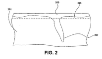
surface 105, which is generally the bottom surface of the recess, and according to embodiments herein, the surface is smooth and facilitates uniform heating of the substrate. Accordingly, in one embodiment, thesurface 105 has a surface roughness Rmax of not greater than about 8.0 microns, such as not greater than about 5.0 microns, or even, not greater than about 2.0 microns. Still, in one particular embodiment, thesurface 105 has a surface roughness Rmax of not greater than about 1.0 micron. - In further reference to the susceptor, referring to
FIG. 2 , a cross-sectional illustration of a portion of a susceptor 200 according to one embodiment is provided. As described, the susceptor includes a silicon impregnated silicon carbide material. According to one embodiment, the composition of thesusceptor body 201 includes not less than about 70 wt% silicon carbide, such as not less than about 80 wt% silicon carbide, or even, not less than about 90 wt% silicon carbide. In one particular embodiment, thesusceptor body 201 includes not less than about 95 wt% silicon carbide. As such, thesusceptor body 201 includes an amount of impregnated silicon, particularly metal silicon impregnated into the silicon carbide during formation. According to one embodiment. thesusceptor body 201 generally includes an amount of silicon not greater than about 30 wt%, such as not greater than about 15 wt% silicon, or even, not greater than about 10 wt% silicon. In a particular embodiment, thesusceptor body 201 includes not greater than about 5.0 wt% silicon. - Impregnating the structure with silicon provides increased density and as such, the body of the susceptor generally has a low degree of porosity, which is primarily closed porosity. Typically, the
susceptor body 201 has a porosity of not greater than about 15 vol%, such as not greater than about 10 vol%, or even, not greater than about 7.5 vol%. Typically, the porosity is not greater than 5 vol%, such as not greater than 3 vol%, or even not greater than 1 vol%. - Referring again to
FIG. 2 , the susceptor 200 further includes anitride layer 203 overlying the body. Generally, thenitride layer 203 is a layer of material that overlies external surfaces of the susceptor body, and particularly thenitride layer 203 can be a continuous film of material overlying otherwise exposed elemental silicon. According to one embodiment, thenitride layer 203 overlies between about 2.0% to about 20% of the external surface area of the susceptor body. - As illustrated,
surface irregularities 207, such as channels or small pores filled with elemental silicon, can exist within thesusceptor body 201, and according to one embodiment, thenitride layer 203 overlies those filledsurface irregularities 207. More particularly, in the case of silicon infiltrated silicon carbide, typically only those portions of elemental silicon that are exposed at the external surface of the susceptor are nitrided, as discussed in more detail below. In one particular embodiment, thenitride layer 203 overlies such irregularities while maintaining a substantially smooth upper surface. - Due to
surface irregularities 207 that may exist on the surface of the body, the thickness of thenitride layer 203 can be measured as an average thickness, illustrated inFIG. 2 bydashed line 205. According to one embodiment, the average thickness of thenitride layer 203 is not less than about 0.2 nm. According to another embodiment, thenitride layer 203 can have an average thickness of not less than about 0.5 nm, or not less than about 1.0 nm, such as not less than about 5.0 nm. According to a particular embodiment, thenitride layer 203 has an average thickness of within a range of between about 0.5 nm and about 2.0 nm. - Generally, the
nitride layer 203 includes a ceramic or metal capable of withstanding temperatures in excess of about 1000°C. In one particular embodiment, thenitride layer 203 includes silicon, such that the majority of thenitride layer 203 includes silicon nitride. According to one embodiment, thenitride layer 203 includes not less than about 90 wt% silicon nitride, such as not less than about 95 wt% silicon nitride, or even not less than about 98 wt% silicon nitride. Still, in another embodiment, thenitride layer 203 is essentially silicon nitride. - Moreover, the
nitride layer 203 is generally a dense layer of material, having a low porosity. The porosity of thenitride layer 203, which is primarily closed porosity, is generally not greater than about 5.0 vol%. According to one embodiment, the porosity of thenitride layer 203 is not greater than about 2.0 vol%, or even not greater than about 1.0 vol%. - In reference to the formation of such susceptors as provided herein, the formation of a siliconized silicon carbide body may be undertaken in accordance with procedures as disclosed in
U.S. Pat. No. 3,951,587 . While the susceptor shape could obviously be formed by several ceramic forming techniques, one particular method is slip casting. Susceptors of practically any length and diameter, and any degree of complexity of shape can easily and economically be performed by slip-casting. Another suitable method may include pressing, such as isostatic pressing, hot pressing, or cold pressing, or combinations thereof. Once the silicon carbide preform has been made, heat treatment is carried out to cause the silicon carbide particles to sinter with varying degrees of recrystallization taking place, depending on the time-temperature conditions employed. - The
application DE 103 29 072 A1 discloses a semiconductor wafer treating element (A) comprising a surface with a silicon carbide layer (C) having a support region for supporting a wafer. The support region has protrusions (1) which contact the wafer and recesses (2) having a silicon carbide layer. A covering surface is provided between the recesses. The recesses have upper surfaces with a surface roughness (Ra) of 0.05-1.3 µm. - Another susceptor is disclosed in
JP 53 066164 A - After the susceptor is so treated, it is then subjected to a second heat treatment to introduce the silicon into the sintered silicon carbide structure, by contacting the sintered parts with silicon at a temperature of about 2150°C in a reducing or at least a non-oxidizing atmosphere, for approximately 10 minutes. This will result in sintered shape becoming partially or wholly impregnated with silicon metal in the amount of from about 5.0 wt% to about 30 wt%, depending on the degree of density of the sintered shape. The silicon metal is generally quite pure i.e. at least 99% pure and preferably 99.9% pure silicon.
- In an alternative method the sintering step as described above is eliminated and the green shaped is directly subject to the siliconizing (silicon impregnation) step, also as described above. In this manner, the silicon carbide particles are sintered and the matrix infiltrated, all in one step. Whether this approach is used, or the former, the porous silicon carbide shapes may be treated with the silicon by immersion, by placing the shapes in contact with silicon allowing capillarity and/or gravity to facilitate impregnation, or by exposing the shaped articles to silicon vapor at 2150°C.
- After the silicon impregnation processing and possibly a machining step, the silicon impregnated shape is subject to a nitridation step to form the final susceptor. Such a nitridation step can include heating the susceptor in a nitrogen atmosphere such that the susceptor is exposed to the nitrogen-containing atmosphere (e.g., nitrogen or ammonia), at elevated temperatures, to effect the formation of a nitride layer by direct reaction with the elemental or free silicon, particularly to form silicon nitride. Typical nitrogen-species (e.g., nitrogen or ammonia) partial pressure is in a range of about 102-106 Pa.
- Generally, the susceptor is heated to a temperature of greater than about 500°C, and generally within a range of between about 800°C and about 1400°C. Such a temperature range facilitates formation of the nitride layer and avoids excessive temperatures which may cause mechanical strain on the susceptor. Alternatively, the processes can include utilization of physical or chemical vapor depositionn susceptors Referring to
FIG. 3 a flow chart is provided that illustrates a process for forming a LED according to one embodiment. As illustrated, the first step includes providing a susceptor having a recess, as described in embodiments herein 301. Notably, the susceptor has a body including a silicon impregnated silicon carbide material and a nitride layer overlying the body. The susceptor can be provided within a growth chamber having atmospheric and temperature controls. Particularly, the susceptor is provided within a MOCVD chamber. - After providing a
suitable susceptor 301, a substrate is placed on thesusceptor 103. The substrate provides a crystalline growth surface for subsequent epitaxial growth of semiconductor layers facilitating the formation of a multilayered LED structure. Generally, the substrate is a single crystal wafer material, generally cut from a boule or other bulk crystalline form. The substrate materials can include elements or compositions such as, silicon carbide, silicon, sapphire, alumina, zinc or gallium nitride (GaN). In one embodiment, the substrate material is a single crystal wafer comprising essentially silicon carbide or sapphire. According to another embodiment, the substrate is a sapphire substrate having a c-plane growth surface which is placed on the susceptor such that the c-plane of the sapphire substrate is exposed for deposition. - The substrate can be placed on the surface of the susceptor. The susceptor can include a recess as described in embodiments herein, and as such, the substrate can be placed within the recess with the growth surface exposed. The recess within the susceptor facilitates precise placement of the substrate on the susceptor and accordingly within the deposition chamber. Additionally, in some applications the substrate is moved or rotated and the recess provides additional engagement of the substrate to the susceptor.
- According to
FIG. 3 , after providing the substrate on thesusceptor 303, one or more underlying layers are formed on thesubstrate 305. Generally, one or more underlying layers can be formed to provide a suitable growth surface template for growth of subsequent semiconductor layers. Such underlying layers can include, for example, one or more buffer layers, films, a mask or patterned layer, or non-coalescing islands or mesas of crystalline material. Particularly, in the context of semiconductor layers grown on foreign substrates, the underlying layer or layers can include a material that has a crystallographic structure that more closely matches the crystallographic structure of the overlying semiconductor layers than the crystallographic structure of the growth surface of the substrate. Suitable materials can include AIN, GaN, AIInN, GaAIN, Si, SiO2, ZnO or a combination thereof. According one particular embodiment, the underlying layer is a buffer layer made of AIN. - The underlying layer or layers can be formed by a deposition process, such as an epitaxial growth process, optionally including photolithographic processing. According to one embodiment, the underlying layer or layers are deposited using MOCVD or also called MOVPE. Additionally, photolithographic patterning can be used to enable epitaxial lateral overgrowth (ELO) processing of the overlying semiconductor layers. The formation of the underlying layer can utilize high temperature processing, such as temperatures greater than about 800°C or even temperatures greater than 1000°C. Alternatively, in one particular embodiment, the underlying layer is a low temperature layer, such as a layer formed at a temperature of less than about 800°C, such as less than about 600°C.
- In the embodiment noted above, the underlying layer is generally provided as a template for crystal growth of subsequent semiconductor layers, and is generally quite thin compared to the semiconducting layers. According to one embodiment, the underlying layer has an average thickness of less than about 400 Angstroms, such as less than about 300 Angstroms, or even less, such as less than about 200 Angstroms. According to another embodiment, the buffer layer has an average thickness within a range of between about 50 Angstroms and about 300 Angstroms.
- Referring again to
FIG. 3 , after forming theunderlying layer 305, a first semiconductor layer can be formed overlying theunderlying layer 307. Generally the first semiconductor layer is one of the first layers facilitating the formation of a light emitting region. The first semiconductor layer can be formed by a deposition process, such as epitaxial growth. According to one embodiment, the first semiconductor layer is formed via a vapor deposition process such as MOCVD or MOVPE. Generally, the forming process is a high temperature process, and according to one embodiment, growth of the first semiconductor layer is conducted at temperatures not less than about 500°C, such as not less than about 700°C, or even at temperatures not less than about 900°C. Still, in one embodiment, the first semiconductor layer is formed at a temperature of not less than about 1000°C. - In further reference to the first semiconductor layer, according to another embodiment, formation of the first semiconductor layer includes formation of a semiconductor layer suitable for forming a blue LED device. As such, in one embodiment, the first semiconductor layer includes a Group III nitride composition. In one embodiment, the first semiconductor layer includes at least one element from the group of elements consisting of Ga, Al, and In. In one particular embodiment, the first semiconductor layer includes GaN.
- Formation of the first semiconductor layer can include adding a dopant to the semiconductor material, such as an n-type or p-type dopant material. According to one embodiment, formation of the first semiconductor layer includes adding a n-type dopant to the material. Generally, the concentration and elements for use as a dopant depends upon the nature of the semiconductor material being doped. In one embodiment, the first semiconductor layer includes GaN and the first semiconductor layer is doped to form a n-type semiconductor layer. In a particular embodiment, the first semiconductor layer includes GaN and a n-type semiconductor layer is formed by doping a substantial portion of the GaN containing layer with a donor element such as silicon (Si). Accordingly, the donor concentration within the GaN layer may be not less than about 1.0x1017 cm-3 at 300 K, such as not less than about 1.0x1018 cm-3 at 300 K.
- In some cases, activation of the dopants within a layer requires a deliberate processing step. As such, according to one embodiment, the method of forming the doped, first semiconductor layer also includes activating the dopant. Such a process can include a thermal annealing in a particular atmosphere at a particular temperature, or an irradiation step utilizing an electron beam, such as for example, low-energy electron beam irradiation (LEEBI) activation.
- Referring again to
FIG. 3 , the method further includes formation of a second semiconductor layer over thefirst semiconductor layer 309. Like the first semiconductor layer, the second semiconductor layer makes possible the formation of the light emitting region. The second semiconductor layer can be formed by deposition, such as an epitaxial growth process, and according to one embodiment, the second semiconductor layer is formed by a vapor deposition process, such as MOCVD or MOVPE. According to another embodiment, formation of the second semiconductor layer is conducted at a temperature of not less than about 500°C, such as not less than about 700°C, or even at a temperature of not less than about 900°C. Still, in one embodiment, the second semiconductor layer is formed at a temperature of not less than about 1000°C. - In reference to the composition of the second semiconductor layer, according to another embodiment, formation of the second semiconductor layer includes formation of a semiconductor layer suitable for forming a blue LED device. As such, in one embodiment, the second semiconductor layer includes a Group III nitride composition. In one embodiment, the second semiconductor layer includes at least one element from the group of elements consisting of Ga, Al, and In. In one particular embodiment, the second semiconductor layer includes GaN.
- In further reference to formation of the second semiconducting layer a dopant can be added to the second semiconductor material. In the particular embodiment described above, because the first semiconductor layer included a n-type dopant the second semiconductor layer includes a p-type dopant. According to a particular embodiment, the second semiconductor layer includes GaN, and a p-type layer is formed by doping the GaN, or at least a substantial portion of the GaN layer, with an acceptor element such as magnesium (Mg). Accordingly, the acceptor concentration within the GaN layer is generally not less than about 1.0x1018 cm-3 at 300 K, such as not less than about 1.0x1019 cm-3 at 300 K. As described in conjunction with the first semiconductor layer, a deliberate activation processing step may be required to electrically activate the acceptors doped into the second semiconductor layer. Such a process can include a thermal annealing in a particular atmosphere at a particular temperature, or an irradiation process.
- In general, because silicon can be used as a dopant, particularly in the context of doping of GaN structures, it is thought that the presence of even a small amount of additional or unaccounted- for silicon within the forming chamber during formation of a layer, which functions as a dopant, can substantially change the characteristics of the device. As such, components within the growth chamber containing silicon are generally undesirable for use in such operations, particularly components containing free silicon or metal silicon.
- It will be appreciated that the above described process illustrated in
FIG. 3 provides a process of forming a layered LED structure according to one embodiment. Typically, one or more additional layers can be formed overlying the substrate, between the first and second semiconductor layers. According to one embodiment, at least one active layer can be formed between the first and second semiconductor layer. - In light of the foregoing,
FIG. 4 provides an illustration of a layered LED structure, according to one embodiment. Particularly, the layered LED structure is a blue LED structure that includes a series of layers among which is asubstrate 401. As described above, the substrate can include a single crystal wafer material, generally cut from a boule or other bulk crystalline form, and typically made from a material such as, silicon carbide, silicon, sapphire, alumina, zinc or gallium nitride. According to a particular embodiment, the substrate material is a single crystal wafer of sapphire, such as sapphire having a c-plane growth surface. - Referring again to
FIG. 4 , the layered LED structure also includeslayer 403, which is generally an underlying layer or buffer layer. According to one embodiment,layer 403 is a low temperature buffer layer and can be grown using MOCVD or MOVPE, at a low temperature, generally less than about 500°C. According to one embodiment, the low temperature buffer layer is thin, having a thickness of not greater than about 300 Angstroms, or even not greater than about 200 Angstroms. Moreover, the low temperature buffer layer can include elements such as Al, Ga, In, and N or a combination thereof. In a particular embodiment, the buffer layer is AIN. -
Overlying layer 403 islayer 405, which according to a particular embodiment is a semiconductor layer. Particularly, in the context of a blue LED structure,layer 405 is a GaN semiconductor layer. More particularly,layer 405 is a n-type GaN semiconductor layer, which is silicon-doped. In such an embodiment, the silicon-doped GaN layer is thicker thanlayer 403, having a thickness greater than about 1.0 micron, typically within a range of between about 1.0 micron and about 5.0 microns. - In further reference to
FIG. 4 , overlyinglayer 405 islayer 407, which according to one embodiment, is an active layer. According to one embodiment, the active layer includes one layer of material, such as a layer forming a double heterojunction structure betweenlayers layer 407 includes a series of layers, which can include a single quantum well structure (SOW) or multiple quantum well (MQW) structure. According to one embodiment, the active layer can include elements, such as Ga, Al, and In or a combination thereof. Particularly suitable compositions of the active layer can include AIInGaN, AIGaN, InGaN, and GaN. In the case of the active layer comprising a plurality of layers to form a quantum well structure, the thickness of each layer can be thin, such as not greater than about 100 Angstroms, or not greater than about 50 Angstroms, and in some cases, not greater than about 25 Angstroms. (10 Angstroms = 1 nanometer) - Referring to the layered LED structure of
FIG. 4 , overlyinglayer 407 islayer 411, which according to one embodiment, is another semiconductor layer. Particularly,layer 411 can be a AIGaN semiconductor layer, and more particularly, a magnesium-doped AIGaN layer. In such an embodiment, the magnesium doped GaN layer can have a thickness of greater than about 500 Angstroms, such as greater than about 750 Angstroms, or even greater than about 1000 Angstroms. -
Overlying layer 411 islayer 413, which according to one embodiment, is another semiconductor layer. Particularly,layer 413 can be a GaN semiconductor layer, and more particularly,layer 413 is a magnesium-doped GaN layer. In such an embodiment, the magnesium doped GaN layer can have a thickness of greater than about 1000 Angstroms, such as greater than about 1500 Angstroms, or even greater than about 2000 Angstroms. -
FIG. 4 further illustratescontacts - According to embodiments described herein, susceptors and methods forming LED devices using such susceptors provide an improvement over state of the art susceptors. Manufacturing of susceptors according to embodiments herein may be carried out with high precision and tight dimensional tolerances, in a cost-effective manner. Further, such susceptors as utilized in LED processing, enable formation of high quality LED devices, at least partly due to superior composition, dimensional stability at high temperature, and dimensional precision, to control and minimize temperature variations that have a negative impact on device quality. Additionally, despite practical concerns to reduce the amount of free silicon in susceptors, embodiments herein having a silicon impregnated silicon carbide structure manage free-silicon content through use of nitridization to bind free silicon. Moreover, susceptors having the combination of features described herein according to certain embodiments also lend themselves to production of LED devices, notably improved production of blue LED devices.
- While the invention has been illustrated and described in the context of specific embodiments, it is not intended to be limited to the details shown, since various modifications and substitutions can be made without departing in any way from the scope of the present invention. For example, additional or equivalent substitutes can be provided and additional or equivalent production steps can be employed. As such, further modifications and equivalents of the invention herein disclosed may occur to persons skilled in the art using no more than routine experimentation, and all such modifications and equivalents are believed to be within the scope of the invention as defined by the following claims.
Claims (15)
- A susceptor for holding a single crystal wafer for LED production comprising:a susceptor body having a recess for receiving a single crystal wafer, wherein the recess has a surface having a surface roughness Rmax of not greater than 10 microns,characterised in that the susceptor body comprises a silicon impregnated silicon carbide; anda nitride layer overlying the susceptor body.
- The susceptor of claim 1, wherein the surface roughness Rmax is not greater than 2.0 microns.
- The susceptor of any one of claims 1-2, wherein the nitride layer comprises silicon nitride,
- The susceptor of any one of claims 1-3, wherein the nitride layer has an average thickness of not less than 0.2 nm.
- The susceptor of any one of claims 1-4, wherein the nitride layer overlies between 2.0% and 20% of the external surface area of the body.
- The susceptor of any one of claims 1-5. wherein the susceptor body has a porosity of not greater than 15 vol%.
- A method of forming a semiconductor LED device comprising;
providing a susceptor comprising, (i) a susceptor body having a recess for receiving a single crystal wafer, wherein the recess has a surface having a surface roughness Rmax of not greater than 10 microns, and wherein the susceptor body comprises a silicon impregnated silicon carbide, and (ii) a nitride layer overlying the susceptor body;
positioning a substrate within the recess of the susceptor body, the substrate having a growth surface;
forming a first semiconductor layer overlying the growth surface; and
forming a second semiconductor layer overlying the first semiconductor layer, wherein a light emitting region is formed between the first semiconductor layer and the second semiconductor layer. - The method of claim 7, wherein the method further comprises forming an underlying layer overlying and in contact with the growth surface of the substrate.
- The method of claim 8, wherein the underlying layer is a buffer layer.
- The method of claim 9, wherein the buffer layer comprises an element selected from the group consisting of gallium, indium and aluminum.
- The method of any one of claims 7-10, wherein forming a first semiconductor layer is carried out by epitaxial growth of a semiconductor material.
- The method of claim 11, wherein the first semiconductor layer comprises a Group III-V nitride semiconductor material.
- The method of claim 11, wherein forming the first semiconductor layer includes doping the semiconductor material to form an n-type semiconductor material.
- The method of any one of claims 7-13, wherein forming the second semiconductor layer is carried out by epitaxial growth of a semiconductor material.
- A method of forming a susceptor, comprising:providing a porous preform comprising silicon carbide;impregnating the porous preform with elemental silicon to form a susceptor body;farming a nitride layer to overlie the susceptor body, wherein the susceptor body has a recess for receiving a single crystal wafer, wherein the recess has a surface having a surface roughness Rmax of not greater than 10 microns.
Applications Claiming Priority (2)
| Application Number | Priority Date | Filing Date | Title |
|---|---|---|---|
| US86522106P | 2006-11-10 | 2006-11-10 | |
| PCT/US2007/084261 WO2008058270A2 (en) | 2006-11-10 | 2007-11-09 | A susceptor and method of forming a led device using such susceptor |
Publications (2)
| Publication Number | Publication Date |
|---|---|
| EP2080221A2 EP2080221A2 (en) | 2009-07-22 |
| EP2080221B1 true EP2080221B1 (en) | 2011-06-15 |
Family
ID=39324157
Family Applications (1)
| Application Number | Title | Priority Date | Filing Date |
|---|---|---|---|
| EP07868710A Not-in-force EP2080221B1 (en) | 2006-11-10 | 2007-11-09 | A susceptor and method of forming a led device using such susceptor |
Country Status (6)
| Country | Link |
|---|---|
| US (1) | US20080110402A1 (en) |
| EP (1) | EP2080221B1 (en) |
| JP (1) | JP2010509778A (en) |
| CN (1) | CN101563771A (en) |
| AT (1) | ATE513311T1 (en) |
| WO (1) | WO2008058270A2 (en) |
Families Citing this family (3)
| Publication number | Priority date | Publication date | Assignee | Title |
|---|---|---|---|---|
| KR20120101633A (en) * | 2009-10-14 | 2012-09-14 | 아사히 가라스 가부시키가이샤 | Jig for semiconductor production and method for producing same |
| US20140256082A1 (en) * | 2013-03-07 | 2014-09-11 | Jehad A. Abushama | Method and apparatus for the formation of copper-indiumgallium selenide thin films using three dimensional selective rf and microwave rapid thermal processing |
| US10490437B2 (en) * | 2015-04-07 | 2019-11-26 | Sumco Corporation | Susceptor, vapor deposition apparatus, vapor deposition method and epitaxial silicon wafer |
Family Cites Families (23)
| Publication number | Priority date | Publication date | Assignee | Title |
|---|---|---|---|---|
| US3951587A (en) * | 1974-12-06 | 1976-04-20 | Norton Company | Silicon carbide diffusion furnace components |
| JPS5366164A (en) * | 1976-11-26 | 1978-06-13 | Hitachi Ltd | Susceptor for semiconductor wafer processing |
| US4795673A (en) * | 1978-01-09 | 1989-01-03 | Stemcor Corporation | Composite material of discontinuous silicon carbide particles and continuous silicon matrix and method of producing same |
| US4633051A (en) * | 1983-11-23 | 1986-12-30 | Advanced Semiconductor Materials America, Inc. | Stable conductive elements for direct exposure to reactive environments |
| JPS6169116A (en) * | 1984-09-13 | 1986-04-09 | Toshiba Ceramics Co Ltd | Susceptor for continuous cvd coating on silicon wafer |
| JPS6447019A (en) * | 1987-08-18 | 1989-02-21 | Denki Kagaku Kogyo Kk | Glassy carbon coated susceptor |
| JPH06287091A (en) * | 1993-02-02 | 1994-10-11 | Ngk Insulators Ltd | Sic-containing far-infrared ray emitter, drier and firing unit |
| JPH0758041A (en) * | 1993-08-20 | 1995-03-03 | Toshiba Ceramics Co Ltd | Susceptor |
| US5837058A (en) * | 1996-07-12 | 1998-11-17 | Applied Materials, Inc. | High temperature susceptor |
| JPH10233529A (en) * | 1997-02-14 | 1998-09-02 | Hewlett Packard Co <Hp> | Nitride semiconductor element and its manufacture |
| US6026589A (en) * | 1998-02-02 | 2000-02-22 | Silicon Valley Group, Thermal Systems Llc | Wafer carrier and semiconductor apparatus for processing a semiconductor substrate |
| US6162543A (en) * | 1998-12-11 | 2000-12-19 | Saint-Gobain Industrial Ceramics, Inc. | High purity siliconized silicon carbide having high thermal shock resistance |
| US6673198B1 (en) * | 1999-12-22 | 2004-01-06 | Lam Research Corporation | Semiconductor processing equipment having improved process drift control |
| EP1341216A1 (en) * | 2000-12-05 | 2003-09-03 | Ibiden Co., Ltd. | Ceramic substrate for semiconductor manufacturing and inspecting devices, and method of manufacturing the ceramic substrate |
| JP3922018B2 (en) * | 2001-12-21 | 2007-05-30 | 株式会社Sumco | Vapor growth apparatus and temperature detection method for vapor growth apparatus |
| US7394043B2 (en) * | 2002-04-24 | 2008-07-01 | Sumitomo Electric Industries, Ltd. | Ceramic susceptor |
| US7255775B2 (en) * | 2002-06-28 | 2007-08-14 | Toshiba Ceramics Co., Ltd. | Semiconductor wafer treatment member |
| JP4278441B2 (en) * | 2002-06-28 | 2009-06-17 | コバレントマテリアル株式会社 | Semiconductor wafer processing components |
| US7256375B2 (en) * | 2002-08-30 | 2007-08-14 | Asm International N.V. | Susceptor plate for high temperature heat treatment |
| EP1654752B1 (en) * | 2003-08-01 | 2011-06-29 | SGL Carbon SE | Holder for supporting wafers during semiconductor manufacture |
| JP4556034B2 (en) * | 2004-03-10 | 2010-10-06 | 学校法人 名城大学 | Method for manufacturing group III nitride semiconductor |
| US20060060145A1 (en) * | 2004-09-17 | 2006-03-23 | Van Den Berg Jannes R | Susceptor with surface roughness for high temperature substrate processing |
| US7632609B2 (en) * | 2005-10-24 | 2009-12-15 | Shin-Etsu Chemical Co., Ltd. | Fabrication method of photomask-blank |
-
2007
- 2007-11-09 WO PCT/US2007/084261 patent/WO2008058270A2/en active Application Filing
- 2007-11-09 EP EP07868710A patent/EP2080221B1/en not_active Not-in-force
- 2007-11-09 CN CNA200780041923XA patent/CN101563771A/en active Pending
- 2007-11-09 JP JP2009536510A patent/JP2010509778A/en active Pending
- 2007-11-09 AT AT07868710T patent/ATE513311T1/en not_active IP Right Cessation
- 2007-11-09 US US11/938,085 patent/US20080110402A1/en not_active Abandoned
Also Published As
| Publication number | Publication date |
|---|---|
| WO2008058270A2 (en) | 2008-05-15 |
| WO2008058270A3 (en) | 2008-07-10 |
| US20080110402A1 (en) | 2008-05-15 |
| EP2080221A2 (en) | 2009-07-22 |
| ATE513311T1 (en) | 2011-07-15 |
| JP2010509778A (en) | 2010-03-25 |
| CN101563771A (en) | 2009-10-21 |
Similar Documents
| Publication | Publication Date | Title |
|---|---|---|
| CN102414796B (en) | Method for fabricating wafer products and method for fabricating gallium nitride semiconductor photonic elements | |
| US7713847B2 (en) | Method for forming AlGaN crystal layer | |
| KR20020076198A (en) | Semiconductor substrate made of group iii nitride, and process for manufacture thereof | |
| WO2009020235A1 (en) | Group iii nitride semiconductor epitaxial substrate | |
| EP2551892A1 (en) | METHOD FOR PRODUCING GaN FILM | |
| TWI252599B (en) | N-type group III nitride semiconductor layered structure | |
| CN105633223B (en) | Semiconductor devices in AlGaN templates, the preparation method of AlGaN templates and AlGaN templates | |
| TW511301B (en) | Method of heat-treating nitride compound semiconductor layer and method of producing semiconductor device | |
| JP4431647B2 (en) | Method for improving surface of single crystal silicon carbide substrate and method for growing single crystal silicon carbide | |
| EP2080221B1 (en) | A susceptor and method of forming a led device using such susceptor | |
| CN100524624C (en) | Group III nitride semiconductor multilayer structure | |
| JPH11135889A (en) | Substrate for crystal growth and light-emitting device using the same | |
| US20230250552A1 (en) | Base substrate for group iii-v compound crystals and production method for same | |
| JPH08186332A (en) | Manufacture of semiconductor element | |
| CN102057463B (en) | Method for manufacturing nitrogen compound semiconductor substrate, nitrogen compound semiconductor substrate, method for manufacturing single crystal SiC substrate, and single crystal SiC substrate | |
| CN103918061A (en) | Crystal layered structure and method for manufacturing same, and semiconductor element | |
| TWI246208B (en) | Group III nitride semiconductor device and light-emitting device using the same | |
| US8853064B2 (en) | Method of manufacturing substrate | |
| CN107039250B (en) | A kind of method of the material of growing gallium nitride on a sapphire substrate, gallium nitride material and application thereof | |
| JP5430467B2 (en) | Group III nitride semiconductor growth substrate, group III nitride semiconductor free-standing substrate, group III nitride semiconductor device, and methods of manufacturing the same | |
| JP5624317B2 (en) | AlN member for compound semiconductor vapor phase growth apparatus and compound semiconductor manufacturing method using the same | |
| JP2008501234A (en) | Light emitting diode | |
| KR20230035353A (en) | Semiconductor substrate with a nitrided interfacial layer | |
| TW569349B (en) | Process of and apparatus for heat-treating II-VI compound semiconductors and semiconductor heat-treated by the process | |
| KR100576850B1 (en) | Manufacturing method of nitride based semiconductor light emitting device |
Legal Events
| Date | Code | Title | Description |
|---|---|---|---|
| PUAI | Public reference made under article 153(3) epc to a published international application that has entered the european phase |
Free format text: ORIGINAL CODE: 0009012 |
|
| 17P | Request for examination filed |
Effective date: 20090508 |
|
| AK | Designated contracting states |
Kind code of ref document: A2 Designated state(s): AT BE BG CH CY CZ DE DK EE ES FI FR GB GR HU IE IS IT LI LT LU LV MC MT NL PL PT RO SE SI SK TR |
|
| DAX | Request for extension of the european patent (deleted) | ||
| GRAP | Despatch of communication of intention to grant a patent |
Free format text: ORIGINAL CODE: EPIDOSNIGR1 |
|
| GRAS | Grant fee paid |
Free format text: ORIGINAL CODE: EPIDOSNIGR3 |
|
| GRAA | (expected) grant |
Free format text: ORIGINAL CODE: 0009210 |
|
| AK | Designated contracting states |
Kind code of ref document: B1 Designated state(s): AT BE BG CH CY CZ DE DK EE ES FI FR GB GR HU IE IS IT LI LT LU LV MC MT NL PL PT RO SE SI SK TR |
|
| REG | Reference to a national code |
Ref country code: GB Ref legal event code: FG4D Ref country code: CH Ref legal event code: EP |
|
| REG | Reference to a national code |
Ref country code: IE Ref legal event code: FG4D |
|
| REG | Reference to a national code |
Ref country code: DE Ref legal event code: R096 Ref document number: 602007015303 Country of ref document: DE Effective date: 20110804 |
|
| REG | Reference to a national code |
Ref country code: NL Ref legal event code: VDEP Effective date: 20110615 |
|
| PG25 | Lapsed in a contracting state [announced via postgrant information from national office to epo] |
Ref country code: SE Free format text: LAPSE BECAUSE OF FAILURE TO SUBMIT A TRANSLATION OF THE DESCRIPTION OR TO PAY THE FEE WITHIN THE PRESCRIBED TIME-LIMIT Effective date: 20110615 Ref country code: LT Free format text: LAPSE BECAUSE OF FAILURE TO SUBMIT A TRANSLATION OF THE DESCRIPTION OR TO PAY THE FEE WITHIN THE PRESCRIBED TIME-LIMIT Effective date: 20110615 |
|
| PG25 | Lapsed in a contracting state [announced via postgrant information from national office to epo] |
Ref country code: CY Free format text: LAPSE BECAUSE OF FAILURE TO SUBMIT A TRANSLATION OF THE DESCRIPTION OR TO PAY THE FEE WITHIN THE PRESCRIBED TIME-LIMIT Effective date: 20110615 Ref country code: FI Free format text: LAPSE BECAUSE OF FAILURE TO SUBMIT A TRANSLATION OF THE DESCRIPTION OR TO PAY THE FEE WITHIN THE PRESCRIBED TIME-LIMIT Effective date: 20110615 Ref country code: LV Free format text: LAPSE BECAUSE OF FAILURE TO SUBMIT A TRANSLATION OF THE DESCRIPTION OR TO PAY THE FEE WITHIN THE PRESCRIBED TIME-LIMIT Effective date: 20110615 Ref country code: AT Free format text: LAPSE BECAUSE OF FAILURE TO SUBMIT A TRANSLATION OF THE DESCRIPTION OR TO PAY THE FEE WITHIN THE PRESCRIBED TIME-LIMIT Effective date: 20110615 Ref country code: SI Free format text: LAPSE BECAUSE OF FAILURE TO SUBMIT A TRANSLATION OF THE DESCRIPTION OR TO PAY THE FEE WITHIN THE PRESCRIBED TIME-LIMIT Effective date: 20110615 Ref country code: GR Free format text: LAPSE BECAUSE OF FAILURE TO SUBMIT A TRANSLATION OF THE DESCRIPTION OR TO PAY THE FEE WITHIN THE PRESCRIBED TIME-LIMIT Effective date: 20110916 |
|
| PG25 | Lapsed in a contracting state [announced via postgrant information from national office to epo] |
Ref country code: BE Free format text: LAPSE BECAUSE OF FAILURE TO SUBMIT A TRANSLATION OF THE DESCRIPTION OR TO PAY THE FEE WITHIN THE PRESCRIBED TIME-LIMIT Effective date: 20110615 Ref country code: NL Free format text: LAPSE BECAUSE OF FAILURE TO SUBMIT A TRANSLATION OF THE DESCRIPTION OR TO PAY THE FEE WITHIN THE PRESCRIBED TIME-LIMIT Effective date: 20110615 |
|
| PG25 | Lapsed in a contracting state [announced via postgrant information from national office to epo] |
Ref country code: CZ Free format text: LAPSE BECAUSE OF FAILURE TO SUBMIT A TRANSLATION OF THE DESCRIPTION OR TO PAY THE FEE WITHIN THE PRESCRIBED TIME-LIMIT Effective date: 20110615 Ref country code: IS Free format text: LAPSE BECAUSE OF FAILURE TO SUBMIT A TRANSLATION OF THE DESCRIPTION OR TO PAY THE FEE WITHIN THE PRESCRIBED TIME-LIMIT Effective date: 20111015 Ref country code: PT Free format text: LAPSE BECAUSE OF FAILURE TO SUBMIT A TRANSLATION OF THE DESCRIPTION OR TO PAY THE FEE WITHIN THE PRESCRIBED TIME-LIMIT Effective date: 20111017 Ref country code: EE Free format text: LAPSE BECAUSE OF FAILURE TO SUBMIT A TRANSLATION OF THE DESCRIPTION OR TO PAY THE FEE WITHIN THE PRESCRIBED TIME-LIMIT Effective date: 20110615 |
|
| PG25 | Lapsed in a contracting state [announced via postgrant information from national office to epo] |
Ref country code: PL Free format text: LAPSE BECAUSE OF FAILURE TO SUBMIT A TRANSLATION OF THE DESCRIPTION OR TO PAY THE FEE WITHIN THE PRESCRIBED TIME-LIMIT Effective date: 20110615 Ref country code: SK Free format text: LAPSE BECAUSE OF FAILURE TO SUBMIT A TRANSLATION OF THE DESCRIPTION OR TO PAY THE FEE WITHIN THE PRESCRIBED TIME-LIMIT Effective date: 20110615 Ref country code: RO Free format text: LAPSE BECAUSE OF FAILURE TO SUBMIT A TRANSLATION OF THE DESCRIPTION OR TO PAY THE FEE WITHIN THE PRESCRIBED TIME-LIMIT Effective date: 20110615 |
|
| PLBE | No opposition filed within time limit |
Free format text: ORIGINAL CODE: 0009261 |
|
| STAA | Information on the status of an ep patent application or granted ep patent |
Free format text: STATUS: NO OPPOSITION FILED WITHIN TIME LIMIT |
|
| 26N | No opposition filed |
Effective date: 20120316 |
|
| PG25 | Lapsed in a contracting state [announced via postgrant information from national office to epo] |
Ref country code: IT Free format text: LAPSE BECAUSE OF FAILURE TO SUBMIT A TRANSLATION OF THE DESCRIPTION OR TO PAY THE FEE WITHIN THE PRESCRIBED TIME-LIMIT Effective date: 20110615 |
|
| PG25 | Lapsed in a contracting state [announced via postgrant information from national office to epo] |
Ref country code: MC Free format text: LAPSE BECAUSE OF NON-PAYMENT OF DUE FEES Effective date: 20111130 Ref country code: DK Free format text: LAPSE BECAUSE OF FAILURE TO SUBMIT A TRANSLATION OF THE DESCRIPTION OR TO PAY THE FEE WITHIN THE PRESCRIBED TIME-LIMIT Effective date: 20110615 |
|
| REG | Reference to a national code |
Ref country code: CH Ref legal event code: PL |
|
| REG | Reference to a national code |
Ref country code: DE Ref legal event code: R097 Ref document number: 602007015303 Country of ref document: DE Effective date: 20120316 |
|
| GBPC | Gb: european patent ceased through non-payment of renewal fee |
Effective date: 20111109 |
|
| PG25 | Lapsed in a contracting state [announced via postgrant information from national office to epo] |
Ref country code: CH Free format text: LAPSE BECAUSE OF NON-PAYMENT OF DUE FEES Effective date: 20111130 Ref country code: LI Free format text: LAPSE BECAUSE OF NON-PAYMENT OF DUE FEES Effective date: 20111130 |
|
| REG | Reference to a national code |
Ref country code: FR Ref legal event code: ST Effective date: 20120731 |
|
| REG | Reference to a national code |
Ref country code: IE Ref legal event code: MM4A |
|
| PG25 | Lapsed in a contracting state [announced via postgrant information from national office to epo] |
Ref country code: GB Free format text: LAPSE BECAUSE OF NON-PAYMENT OF DUE FEES Effective date: 20111109 Ref country code: IE Free format text: LAPSE BECAUSE OF NON-PAYMENT OF DUE FEES Effective date: 20111109 |
|
| PG25 | Lapsed in a contracting state [announced via postgrant information from national office to epo] |
Ref country code: FR Free format text: LAPSE BECAUSE OF NON-PAYMENT OF DUE FEES Effective date: 20111130 |
|
| PGFP | Annual fee paid to national office [announced via postgrant information from national office to epo] |
Ref country code: DE Payment date: 20121107 Year of fee payment: 6 |
|
| PG25 | Lapsed in a contracting state [announced via postgrant information from national office to epo] |
Ref country code: MT Free format text: LAPSE BECAUSE OF FAILURE TO SUBMIT A TRANSLATION OF THE DESCRIPTION OR TO PAY THE FEE WITHIN THE PRESCRIBED TIME-LIMIT Effective date: 20110615 |
|
| PG25 | Lapsed in a contracting state [announced via postgrant information from national office to epo] |
Ref country code: ES Free format text: LAPSE BECAUSE OF FAILURE TO SUBMIT A TRANSLATION OF THE DESCRIPTION OR TO PAY THE FEE WITHIN THE PRESCRIBED TIME-LIMIT Effective date: 20110926 |
|
| PG25 | Lapsed in a contracting state [announced via postgrant information from national office to epo] |
Ref country code: LU Free format text: LAPSE BECAUSE OF NON-PAYMENT OF DUE FEES Effective date: 20111109 |
|
| PG25 | Lapsed in a contracting state [announced via postgrant information from national office to epo] |
Ref country code: BG Free format text: LAPSE BECAUSE OF FAILURE TO SUBMIT A TRANSLATION OF THE DESCRIPTION OR TO PAY THE FEE WITHIN THE PRESCRIBED TIME-LIMIT Effective date: 20110915 |
|
| PG25 | Lapsed in a contracting state [announced via postgrant information from national office to epo] |
Ref country code: TR Free format text: LAPSE BECAUSE OF FAILURE TO SUBMIT A TRANSLATION OF THE DESCRIPTION OR TO PAY THE FEE WITHIN THE PRESCRIBED TIME-LIMIT Effective date: 20110615 |
|
| PG25 | Lapsed in a contracting state [announced via postgrant information from national office to epo] |
Ref country code: HU Free format text: LAPSE BECAUSE OF FAILURE TO SUBMIT A TRANSLATION OF THE DESCRIPTION OR TO PAY THE FEE WITHIN THE PRESCRIBED TIME-LIMIT Effective date: 20110615 |
|
| REG | Reference to a national code |
Ref country code: DE Ref legal event code: R119 Ref document number: 602007015303 Country of ref document: DE Effective date: 20140603 |
|
| PG25 | Lapsed in a contracting state [announced via postgrant information from national office to epo] |
Ref country code: DE Free format text: LAPSE BECAUSE OF NON-PAYMENT OF DUE FEES Effective date: 20140603 |