EP2079130A1 - Antenna module - Google Patents
Antenna module Download PDFInfo
- Publication number
- EP2079130A1 EP2079130A1 EP08169884A EP08169884A EP2079130A1 EP 2079130 A1 EP2079130 A1 EP 2079130A1 EP 08169884 A EP08169884 A EP 08169884A EP 08169884 A EP08169884 A EP 08169884A EP 2079130 A1 EP2079130 A1 EP 2079130A1
- Authority
- EP
- European Patent Office
- Prior art keywords
- radiating
- sub
- edge
- antenna module
- grounding
- Prior art date
- Legal status (The legal status is an assumption and is not a legal conclusion. Google has not performed a legal analysis and makes no representation as to the accuracy of the status listed.)
- Withdrawn
Links
- 230000005540 biological transmission Effects 0.000 claims abstract description 44
- 239000000758 substrate Substances 0.000 claims abstract description 8
- 230000000694 effects Effects 0.000 description 7
- 238000010586 diagram Methods 0.000 description 6
- 238000004891 communication Methods 0.000 description 5
- 238000013461 design Methods 0.000 description 3
- 230000008901 benefit Effects 0.000 description 2
- 238000005516 engineering process Methods 0.000 description 2
- 238000005259 measurement Methods 0.000 description 2
- 239000002184 metal Substances 0.000 description 2
- 238000011161 development Methods 0.000 description 1
- 239000003822 epoxy resin Substances 0.000 description 1
- 239000011152 fibreglass Substances 0.000 description 1
- 238000004519 manufacturing process Methods 0.000 description 1
- 238000012986 modification Methods 0.000 description 1
- 230000004048 modification Effects 0.000 description 1
- 229920000647 polyepoxide Polymers 0.000 description 1
- 230000005855 radiation Effects 0.000 description 1
Images





Classifications
-
- H—ELECTRICITY
- H01—ELECTRIC ELEMENTS
- H01Q—ANTENNAS, i.e. RADIO AERIALS
- H01Q9/00—Electrically-short antennas having dimensions not more than twice the operating wavelength and consisting of conductive active radiating elements
- H01Q9/04—Resonant antennas
- H01Q9/30—Resonant antennas with feed to end of elongated active element, e.g. unipole
- H01Q9/40—Element having extended radiating surface
-
- H—ELECTRICITY
- H01—ELECTRIC ELEMENTS
- H01Q—ANTENNAS, i.e. RADIO AERIALS
- H01Q1/00—Details of, or arrangements associated with, antennas
- H01Q1/48—Earthing means; Earth screens; Counterpoises
Definitions
- the invention relates to an antenna module and, more particularly, to an antenna module having a wide bandwidth characteristic.
- the wireless communication is various, such as the wireless wide area network (WWAN), the wireless metropolitan area network (WMAN), the wireless local area network (WLAN), the wireless personal area network (WPAN) or the Bluetooth, and each type of communication has its corresponding operating bandwidth.
- WWAN wireless wide area network
- WMAN wireless metropolitan area network
- WLAN wireless local area network
- WPAN wireless personal area network
- Bluetooth each type of communication has its corresponding operating bandwidth.
- the wireless communication technology employs various antennas to receive or send signals of corresponding bandwidths.
- a radio system operates within multiple bandwidths, most antennas utilize a plurality of groups of independent antennas to achieve the objective of antenna diversity.
- the complexity of the system rises greatly, and the space utilization ration drops greatly.
- the invention is related to an antenna module, and the antenna module has a wide bandwidth characteristic via the design of shapes of a radiating element and a grounding element.
- an antenna module includes a dielectric substrate, a grounding element, a transmission element and a radiating element.
- the dielectric substrate has a first surface and a second surface.
- the grounding element is disposed at the first surface.
- the transmission element and the radiating element are disposed at the second surface.
- the radiating element includes a first sub-radiating element.
- the first sub-radiating element has a first side and a second side. The first sub-radiating element is connected to the transmission element at the first side, and the width of the first sub-radiating element gradually becomes larger from the first side toward the second side.
- the equivalent impedance of the first sub-radiating element is generally equal to the impedance of the transmission process when wireless signals from the lowest frequency to the highest frequency are transmitted. Therefore, the feedback quantity of the wireless signals of the whole bandwidth is below a standard value defined by a used protocol to obtain a wide bandwidth effect when the wireless signals from the lowest frequency to the highest frequency are transmitted.
- FIG. 1 is a schematic diagram showing an antenna module of the first embodiment of the invention
- FIG. 2A is a top view showing the antenna module in FIG. 1 ;
- FIG. 2B is a schematic diagram showing the relationship between the radiating element, the grounding element and the transmission element and the first surface of the antenna module in FIG. 1 ;
- FIG. 3 is a schematic diagram showing a return loss measurement chart of the antenna module in FIG. 1 ;
- FIG. 4 is a top view showing an antenna module of the second embodiment of the invention.
- FIG. 5 is a top view showing an antenna module of the third embodiment of the invention.
- FIG. 6 is a top view showing an antenna module of the fourth embodiment of the invention.
- FIG. 7 is a top view showing an antenna module of the fifth embodiment of the invention.
- FIG. 1 is a schematic diagram showing an antenna module 100 of the first embodiment of the invention.
- the antenna module 100 includes a dielectric substrate 110, a grounding element 120, a transmission element 140 and a radiating element 130.
- the dielectric substrate 110 is made of, for example, epoxide resin or fiberglass.
- the dielectric substrate 110 has a first surface 110a and a second surface 110b.
- the grounding element 120 is disposed at the first surface 110a.
- the transmission element 140 and the radiating element 130 are disposed at the second surface 110b.
- the grounding element 120, the transmission element 140 and the radiating element 130 may be, for example, printed metal layers or additionally attached metal sheets.
- the radiating element 130 at least includes a first sub-radiating element 131.
- the first sub-radiating element 131 has a first side S1 and a second side S2 opposite to the first side S1 (in FIG. 1 , the first side S1 and the second side S2 are denoted with broken lines).
- the first sub-radiating element 131 is connected to the transmission element 140 at the first side S1, and the width of the first sub-radiating element 131 gradually becomes larger from the first side S1 toward the second side S2.
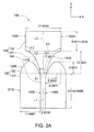
- FIG. 2A is a top view showing the antenna module 100 in FIG. 1 .
- the transmission element 140 has a transmission edge 140S
- the first sub-radiating element 131 has a first radiating edge 131S.
- the transmission edge 140S is connected to the first radiating edge 131S
- the first radiating edge 131S connects the first side S1 with the second side S2.
- the transmission element 140 has two transmission edges 140S, and the first sub-radiating element 131 has two first radiating edges 131S.
- the two transmission edges 140S are symmetric with respect to a central axis L1 of the transmission element 140.
- the two first radiating edges 131 S are symmetric with respect to a symmetric axis L2 of the first sub-radiating element 131. That is, the transmission element 140 and the first sub-radiating element 131 of the embodiment are symmetric structures.
- the first radiating edge 131 S is a smooth curve in shape.
- the two first radiating edges 131S are close to each other at the first side S1, and they are far away from each other at the second side S2. That is, the distance between the two first radiating edges 131S at the first side S1 is smaller than the distance between the two first radiating edges 131S at the second side S2.
- the distance between the two first radiating edges 131 S gradually increases from the first side S1 toward the second side S2. That is, the first sub-radiating element 131 is crateriform.
- the smooth curve is, for example, part of an elliptical curve, part of a circular curve, part of a parabolic curve or other curve.
- each of the first radiating edges 131 S is a quarter elliptical curve in shape.
- the elliptical curve has a major axis and a minor axis, and the ratio of the major axis and the minor axis is between 1.3 and 3.
- the ratio of the major axis and the minor axis preferably is between 1.5 and 2.
- the angle 61 between the transmission edge 140S and the first radiating edge 131 S is greater than ninety degrees. That is, the transmission edge 140S and the first radiating edge 131 S do not form a sharp angle at their connection place.
- the transmission edge 140S and the first radiating edge 131 S may be smooth straight lines or smooth curves, and the connection place of the transmission edge 140S and the first radiating edge 131 S also is smooth. In this way, wireless signals can be smoothly emitted out (or fed in), and they cannot be greatly fed back (or reflected) at some position.
- the radiating element 130 of the embodiment further includes a second sub-radiating element 132.
- the second sub-radiating element 132 has a second radiating edge 132S, and the second radiating edge 132S is connected to the first radiating edge 131 S.
- the second radiating edge 132S is a straight line in shape.
- the second sub-radiating element 132 of the embodiment may be a rectangular structure.
- the second sub-radiating element 132 is used to adjust the corresponding equivalent impedance of the first sub-radiating element 131 at the second side S2 to allow the first sub-radiating element 131 to satisfy an impedance matching requirement at the second side S2.
- the angle ⁇ 2 between the second radiating edge 132S and the first radiating edge 131 S also is greater than ninety degrees.
- the transmission edge 140S, the first radiating edge 131S and the second radiating edge 132S may be straight lines or smooth curves in shape, and the transmission edge 140S, the first radiating edge 131S and the second radiating edge 132S do not form sharp angles at their connection places (the connection places even are smooth). Therefore, the wireless signals can be smoothly emitted out (or fed in), and they cannot be greatly fed back (or reflected) at some position.
- the second sub-radiating element 132 has two second radiating edges 132S, and the two second radiating edges 132S are symmetric with respect to the symmetric axis L3 of the second sub-radiating element 132. Therefore, the second sub-radiating element 132 also is a symmetric structure.
- the grounding element 120 includes a first sub-grounding element 121 and at least a second sub-grounding element 122.
- the transmission element 140 is disposed above the first sub-grounding element 121.
- the first sub-grounding element 121 has a first grounding edge 121S.
- the first sub-grounding element 121 is a rectangular structure.
- the area of the first sub-grounding element 121 is larger than the area of the transmission element 140.
- the second sub-grounding element 122 is connected to the first sub-grounding element 121.
- the second sub-grounding element 122 has a grounding edge 122S.
- the grounding edge 122S is connected to the top of the first sub-grounding element 121.
- FIG. 2B is a schematic diagram showing the relationship between the radiating element 130, the grounding element 120 and the transmission element 140 and the first surface 110a of the antenna module 100 in FIG. 1 .
- the first surface 110a where the grounding element 120 is disposed is divided into a first area A1 and a second area A2.
- the grounding element 120 (including the first sub-grounding element 121 and the second sub-grounding element 122) is disposed in the first area A1, and the second area A2 is the other area of the first surface 110a except the first area A1.
- the transmission element 140 is disposed above the first area A1.
- the first sub-radiating element 131 and the second sub-radiating element 132 are disposed above the second area A2. That is, the transmission element 140 overlaps the grounding element 120.
- the first sub-radiating element 131 and the second sub-radiating element 132 do not overlap the grounding element 120.
- the grounding element 120 of the embodiment includes two second grounding elements 122.
- the two second grounding elements 122 are located at two sides of the first sub-radiating element 131, respectively.
- the grounding edge 122S is adjacent to the first radiating edge 131 S.
- the grounding edge 122S is preferred to be similar to the first radiating edge 131 S in shape. Then, when the wireless signals form a resonance mode between the first radiating edge 131S and the grounding edge 122S, the energy of the wireless signals can be maintained at a certain degree and not be lost.
- the first radiating edge 131S is a quarter elliptical curve
- the grounding edge 122S also is part of an elliptical curve in shape and is preferred to be a half of an elliptical curve in shape.
- the transmission element 140S has a first distance D1 of, for example, 20.0469 millimeters.
- the first radiating edge 131 S has a semi-major axis of, for example, 13.0931 millimeters and a semi-minor axis of, for example, 9.0411 millimeters. That is, the ratio of the major axis to the minor axis is about 1.45.
- the first radiating edge 131S has a second length D2 of, for example, 17.52 millimeters.
- the width of the first sub-radiating element 131 at the first side S1 is, for example, 2.9300 millimeters, and the width of the first sub-radiating element 131 at the second side S2 is, for example, 21.0700 millimeters.
- the second radiating edge 132S of the second sub-radiating element 132 has a third length D3 of, for example, 11.3316 millimeters.
- the length and width of the first sub-grounding element 121 are 26.8234 millimeters and 20.0469 millimeters, respectively.
- Each of the second sub-grounding elements 122 is a half of an ellipse in shape, the semi-major axis and the semi-minor axis of the ellipse are, for example, 6.9531 millimeters and 5.5092 millimeters, respectively.
- FIG. 3 is a schematic diagram showing a return loss measurement chart of the antenna module 100 in FIG. 1 .
- the equivalent impedance of the first sub-radiating element 131 is related to the greatest width (at the second side S2) of the first sub-radiating element 131.
- the equivalent impedance of the first sub-radiating element 131 is related to the smallest width (at the first side S1) of the first sub-radiating element 131.
- the equivalent impedance of the first sub-radiating element 131 is related to a middle width (which is located between the first side S1 and the second side S2) between the greatest width and the smallest width.
- the equivalent impedance of the first sub-radiating element 131 is generally equal to the impedance of the transmission process when wireless signals from the lowest frequency to the highest frequency are transmitted. Therefore, the feedback quantity of the wireless signals of the whole bandwidth is below a standard value defined by a used protocol to obtain a wide bandwidth effect when the wireless signals from the lowest frequency to the highest frequency are transmitted.
- the antenna module 100 can preferably receive wireless signals within the bandwidth between 2.50408GHz and 10.000GHz.
- the antenna module 100 is suitable for the wireless wide area network (WWAN), the wireless metropolitan area network (WMAN), the wireless local area network (WLAN), the wireless personal area network (WPAN) or the Bluetooth.
- WWAN wireless wide area network
- WMAN wireless metropolitan area network
- WLAN wireless local area network
- WPAN wireless personal area network
- the 802.11 protocol, the 802.11b protocol, the 802.11a protocol and the 802.11g protocol are operated at 2.4GHz, 2.4GHz, 5GHz and 2.4GHz, respectively.
- the antenna module 100 of the embodiment can operate at all the above frequencies.
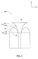
- FIG. 4 is a top view showing an antenna module 200 of the second embodiment of the invention.
- the difference between the antenna module 200 of the embodiment and the antenna module 100 of the first embodiment is that the radiating element 230 of the embodiment does not have the second sub-radiating element 132, and the same components are not described for concise purpose.
- Designers can extend lengths of the first sub-radiating element 231 and the first radiating edge 231 S and remove the second sub-radiating element 132 according to a design requirement. Under the condition that the width of the first sub-radiating element 231 gradually increases from the first side S1 toward the second side S2, the first sub-radiating element 231 satisfies with the impedance matching at every point. Any point of the first sub-radiating element 231 between the first side S1 and the second side S2 can cooperate with the grounding element 120 to generate a good resonance mode to obtain a wide bandwidth effect.
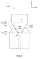
- FIG. 5 is a top view showing an antenna module 300 of the third embodiment of the invention.
- the difference between the antenna module 300 of the embodiment and the antenna module 100 of the first embodiment is shapes of a first radiating edge 331 S and a grounding edge 322S, and the same components are not described for concise purpose.
- the first radiating edge 331 S is a straight line in shape. That is, the first sub-radiating element 331 of the radiating element 330 is trapezoid. Under the condition that the width of the trapezoid first sub-radiating element 331 gradually increases from the first side S1 toward the second side S2, the first sub-radiating element 331 satisfies with the impedance matching at every point. Any point of the first sub-radiating element 331 between the first side S1 and the second side S2 can cooperate with the grounding element 320 to generate a good resonance mode to obtain a wide bandwidth effect.
- FIG. 6 is a top view showing an antenna module 400 of the fourth embodiment of the invention.
- the difference between the antenna module 400 of the embodiment and the antenna module 100 of the first embodiment is shapes of a first radiating edge 431 S and a grounding edge 422S, and the same components are not described for concise purpose.
- the first radiating edge 431S of the embodiment is a polygonal line in shape. That is, the first sub-radiating element 431 of the radiating element 430 is polygonal. Under the condition that the width of the polygonal first sub-radiating element 431 gradually increases from the first side S1 toward the second side S2, the first sub-radiating element 431 satisfies with the impedance matching at every point. Any point of the first sub-radiating element 431 between the first side S1 and the second side S2 can cooperate with the grounding element 420 to generate a good resonance mode to obtain a wide bandwidth effect.
- FIG. 7 is a top view showing an antenna module 500 of the fifth embodiment of the invention.
- the difference between the antenna module 500 of the embodiment and the antenna module 100 of the first embodiment is shapes of a first radiating edge 531 S and a grounding edge 522S, and the same components are not described for concise purpose.
- the first radiating edge 531 S of the embodiment is stepped. Under the condition that the width of the stepped first sub-radiating element 531 gradually increases from the first side S1 toward the second side S2, the first sub-radiating element 531 satisfies with the impedance matching at every point. Any point of the first sub-radiating element 531 between the first side S1 and the second side S2 can cooperate with the grounding element 520 to generate a good resonance mode to obtain a wide bandwidth effect.
- the antenna module of the embodiment of the invention employs the design of the shapes of the radiating element and the grounding element to allow the antenna module to obtain the wide bandwidth effect. Furthermore, the antenna module of the embodiment is a type of circuit board, and it can be directly used on the circuit board that an electronic device originally has. Then, the antenna module has a low manufacture cost and can be conveniently assembled.
Landscapes
- Details Of Aerials (AREA)
Abstract
An antenna module includes a dielectric substrate, a grounding element, a transmission element and a radiating element. The dielectric substrate has a first surface and a second surface. The grounding element is disposed on the first surface. The transmission element and the radiating element are disposed on the second surface. The radiating element includes a first sub-radiating element having a first side and a second side. The first sub-radiation element is connected to the transmission element at the first side, and the width of the first sub-radiating element gradually becomes larger from the first side toward the second side.
Description
- This application claims the benefit of Taiwan application Serial No.
0 97101355, filed Jan. 14, 2008 - The invention relates to an antenna module and, more particularly, to an antenna module having a wide bandwidth characteristic.
- Along with the development of the wireless communication technology, more and more electronic products have various communication functions. The wireless communication is various, such as the wireless wide area network (WWAN), the wireless metropolitan area network (WMAN), the wireless local area network (WLAN), the wireless personal area network (WPAN) or the Bluetooth, and each type of communication has its corresponding operating bandwidth.
- The wireless communication technology employs various antennas to receive or send signals of corresponding bandwidths. When a radio system operates within multiple bandwidths, most antennas utilize a plurality of groups of independent antennas to achieve the objective of antenna diversity. However, in this way, the complexity of the system rises greatly, and the space utilization ration drops greatly.
- Even if two groups of antennas are combined to form a complex antenna, the interference between the two groups of antennas often seriously affects the radiating bandwidth. The original performance of each group of antenna even reduces.
- The invention is related to an antenna module, and the antenna module has a wide bandwidth characteristic via the design of shapes of a radiating element and a grounding element.
- According to one aspect of the invention, an antenna module is provided. The antenna module includes a dielectric substrate, a grounding element, a transmission element and a radiating element. The dielectric substrate has a first surface and a second surface. The grounding element is disposed at the first surface. The transmission element and the radiating element are disposed at the second surface. The radiating element includes a first sub-radiating element. The first sub-radiating element has a first side and a second side. The first sub-radiating element is connected to the transmission element at the first side, and the width of the first sub-radiating element gradually becomes larger from the first side toward the second side.
- By gradually increasing the width of the first sub-radiating element, the equivalent impedance of the first sub-radiating element is generally equal to the impedance of the transmission process when wireless signals from the lowest frequency to the highest frequency are transmitted. Therefore, the feedback quantity of the wireless signals of the whole bandwidth is below a standard value defined by a used protocol to obtain a wide bandwidth effect when the wireless signals from the lowest frequency to the highest frequency are transmitted.
- These and other features, aspects, and advantages of the present invention will become better understood with regard to the following description, appended claims, and accompanying drawings.
-
FIG. 1 is a schematic diagram showing an antenna module of the first embodiment of the invention; -
FIG. 2A is a top view showing the antenna module inFIG. 1 ; -
FIG. 2B is a schematic diagram showing the relationship between the radiating element, the grounding element and the transmission element and the first surface of the antenna module inFIG. 1 ; -
FIG. 3 is a schematic diagram showing a return loss measurement chart of the antenna module inFIG. 1 ; -
FIG. 4 is a top view showing an antenna module of the second embodiment of the invention; -
FIG. 5 is a top view showing an antenna module of the third embodiment of the invention; -
FIG. 6 is a top view showing an antenna module of the fourth embodiment of the invention; and -
FIG. 7 is a top view showing an antenna module of the fifth embodiment of the invention. -
FIG. 1 is a schematic diagram showing anantenna module 100 of the first embodiment of the invention. Theantenna module 100 includes adielectric substrate 110, agrounding element 120, atransmission element 140 and aradiating element 130. Thedielectric substrate 110 is made of, for example, epoxide resin or fiberglass. Thedielectric substrate 110 has afirst surface 110a and asecond surface 110b. Thegrounding element 120 is disposed at thefirst surface 110a. Thetransmission element 140 and theradiating element 130 are disposed at thesecond surface 110b. Thegrounding element 120, thetransmission element 140 and theradiating element 130 may be, for example, printed metal layers or additionally attached metal sheets. - The
radiating element 130 at least includes afirst sub-radiating element 131. Thefirst sub-radiating element 131 has a first side S1 and a second side S2 opposite to the first side S1 (inFIG. 1 , the first side S1 and the second side S2 are denoted with broken lines). Thefirst sub-radiating element 131 is connected to thetransmission element 140 at the first side S1, and the width of thefirst sub-radiating element 131 gradually becomes larger from the first side S1 toward the second side S2. -
FIG. 2A is a top view showing theantenna module 100 inFIG. 1 . In detail, thetransmission element 140 has atransmission edge 140S, and thefirst sub-radiating element 131 has a firstradiating edge 131S. Thetransmission edge 140S is connected to the firstradiating edge 131S, and the firstradiating edge 131S connects the first side S1 with the second side S2. - In the embodiment, the
transmission element 140 has twotransmission edges 140S, and thefirst sub-radiating element 131 has two firstradiating edges 131S. The twotransmission edges 140S are symmetric with respect to a central axis L1 of thetransmission element 140. The two firstradiating edges 131 S are symmetric with respect to a symmetric axis L2 of thefirst sub-radiating element 131. That is, thetransmission element 140 and thefirst sub-radiating element 131 of the embodiment are symmetric structures. - The first
radiating edge 131 S is a smooth curve in shape. The two firstradiating edges 131S are close to each other at the first side S1, and they are far away from each other at the second side S2. That is, the distance between the two firstradiating edges 131S at the first side S1 is smaller than the distance between the two firstradiating edges 131S at the second side S2. The distance between the two firstradiating edges 131 S gradually increases from the first side S1 toward the second side S2. That is, thefirst sub-radiating element 131 is crateriform. - The smooth curve is, for example, part of an elliptical curve, part of a circular curve, part of a parabolic curve or other curve. In the embodiment, each of the first
radiating edges 131 S is a quarter elliptical curve in shape. The elliptical curve has a major axis and a minor axis, and the ratio of the major axis and the minor axis is between 1.3 and 3. The ratio of the major axis and the minor axis preferably is between 1.5 and 2. - The angle 61 between the
transmission edge 140S and the firstradiating edge 131 S is greater than ninety degrees. That is, thetransmission edge 140S and the firstradiating edge 131 S do not form a sharp angle at their connection place. Thetransmission edge 140S and thefirst radiating edge 131 S may be smooth straight lines or smooth curves, and the connection place of thetransmission edge 140S and thefirst radiating edge 131 S also is smooth. In this way, wireless signals can be smoothly emitted out (or fed in), and they cannot be greatly fed back (or reflected) at some position. - The radiating
element 130 of the embodiment further includes a secondsub-radiating element 132. The secondsub-radiating element 132 has asecond radiating edge 132S, and thesecond radiating edge 132S is connected to thefirst radiating edge 131 S. Thesecond radiating edge 132S is a straight line in shape. The secondsub-radiating element 132 of the embodiment may be a rectangular structure. The secondsub-radiating element 132 is used to adjust the corresponding equivalent impedance of the firstsub-radiating element 131 at the second side S2 to allow the firstsub-radiating element 131 to satisfy an impedance matching requirement at the second side S2. - In the embodiment, the angle θ2 between the
second radiating edge 132S and thefirst radiating edge 131 S also is greater than ninety degrees. Thetransmission edge 140S, thefirst radiating edge 131S and thesecond radiating edge 132S may be straight lines or smooth curves in shape, and thetransmission edge 140S, thefirst radiating edge 131S and thesecond radiating edge 132S do not form sharp angles at their connection places (the connection places even are smooth). Therefore, the wireless signals can be smoothly emitted out (or fed in), and they cannot be greatly fed back (or reflected) at some position. - The second
sub-radiating element 132 has two second radiating edges 132S, and the two second radiating edges 132S are symmetric with respect to the symmetric axis L3 of the secondsub-radiating element 132. Therefore, the secondsub-radiating element 132 also is a symmetric structure. - As shown in
FIG.1 andFIG. 2A , as for thegrounding element 120, it includes a firstsub-grounding element 121 and at least a secondsub-grounding element 122. Thetransmission element 140 is disposed above the firstsub-grounding element 121. The firstsub-grounding element 121 has afirst grounding edge 121S. In the embodiment, the firstsub-grounding element 121 is a rectangular structure. The area of the firstsub-grounding element 121 is larger than the area of thetransmission element 140. - The second
sub-grounding element 122 is connected to the firstsub-grounding element 121. The secondsub-grounding element 122 has agrounding edge 122S. Thegrounding edge 122S is connected to the top of the firstsub-grounding element 121. -
FIG. 2B is a schematic diagram showing the relationship between the radiatingelement 130, thegrounding element 120 and thetransmission element 140 and thefirst surface 110a of theantenna module 100 inFIG. 1 . Thefirst surface 110a where thegrounding element 120 is disposed is divided into a first area A1 and a second area A2. The grounding element 120 (including the firstsub-grounding element 121 and the second sub-grounding element 122) is disposed in the first area A1, and the second area A2 is the other area of thefirst surface 110a except the first area A1. As shown inFIG. 2B , thetransmission element 140 is disposed above the first area A1. The firstsub-radiating element 131 and the secondsub-radiating element 132 are disposed above the second area A2. That is, thetransmission element 140 overlaps thegrounding element 120. The firstsub-radiating element 131 and the secondsub-radiating element 132 do not overlap thegrounding element 120. - The
grounding element 120 of the embodiment includes twosecond grounding elements 122. The twosecond grounding elements 122 are located at two sides of the firstsub-radiating element 131, respectively. Thegrounding edge 122S is adjacent to thefirst radiating edge 131 S. Thegrounding edge 122S is preferred to be similar to thefirst radiating edge 131 S in shape. Then, when the wireless signals form a resonance mode between thefirst radiating edge 131S and thegrounding edge 122S, the energy of the wireless signals can be maintained at a certain degree and not be lost. - In the embodiment, the
first radiating edge 131S is a quarter elliptical curve, and thegrounding edge 122S also is part of an elliptical curve in shape and is preferred to be a half of an elliptical curve in shape. - In the embodiment, the
transmission element 140S has a first distance D1 of, for example, 20.0469 millimeters. - The
first radiating edge 131 S has a semi-major axis of, for example, 13.0931 millimeters and a semi-minor axis of, for example, 9.0411 millimeters. That is, the ratio of the major axis to the minor axis is about 1.45. Thefirst radiating edge 131S has a second length D2 of, for example, 17.52 millimeters. The width of the firstsub-radiating element 131 at the first side S1 is, for example, 2.9300 millimeters, and the width of the firstsub-radiating element 131 at the second side S2 is, for example, 21.0700 millimeters. - The
second radiating edge 132S of the secondsub-radiating element 132 has a third length D3 of, for example, 11.3316 millimeters. - The length and width of the first
sub-grounding element 121 are 26.8234 millimeters and 20.0469 millimeters, respectively. - Each of the second
sub-grounding elements 122 is a half of an ellipse in shape, the semi-major axis and the semi-minor axis of the ellipse are, for example, 6.9531 millimeters and 5.5092 millimeters, respectively. -
FIG. 3 is a schematic diagram showing a return loss measurement chart of theantenna module 100 inFIG. 1 . Generally speaking, the radiation wavelength that theantenna module 100 can operate with is determined by equation (1):
- Wherein λ is the wavelength, f is the frequency, and ε r is the dielectric coefficient. Therefore, the lowest frequency that the
antenna module 100 can operate at is determined by the sum of the second length D2 and the third length D3 (that is, 17.52 + 11.3316 = 28.8516 millimeters). - In the whole bandwidth, when the wireless signal having the lowest frequency is transmitted, the equivalent impedance of the first
sub-radiating element 131 is related to the greatest width (at the second side S2) of the firstsub-radiating element 131. When the wireless signal having the highest frequency is transmitted, the equivalent impedance of the firstsub-radiating element 131 is related to the smallest width (at the first side S1) of the firstsub-radiating element 131. When a wireless signals having an intermediate frequency between the highest frequency and the lowest frequency is transmitted, the equivalent impedance of the firstsub-radiating element 131 is related to a middle width (which is located between the first side S1 and the second side S2) between the greatest width and the smallest width. - By gradually increasing the width of the first
sub-radiating element 131, the equivalent impedance of the firstsub-radiating element 131 is generally equal to the impedance of the transmission process when wireless signals from the lowest frequency to the highest frequency are transmitted. Therefore, the feedback quantity of the wireless signals of the whole bandwidth is below a standard value defined by a used protocol to obtain a wide bandwidth effect when the wireless signals from the lowest frequency to the highest frequency are transmitted. - As shown in
FIG. 3 , all return losses are below -10dB when the antenna module operates within a bandwidth between 2.50408GHz and 10.000GHz. Therefore, theantenna module 100 can preferably receive wireless signals within the bandwidth between 2.50408GHz and 10.000GHz. Thus, theantenna module 100 is suitable for the wireless wide area network (WWAN), the wireless metropolitan area network (WMAN), the wireless local area network (WLAN), the wireless personal area network (WPAN) or the Bluetooth. For example, in the WPAN, the 802.11 protocol, the 802.11b protocol, the 802.11a protocol and the 802.11g protocol are operated at 2.4GHz, 2.4GHz, 5GHz and 2.4GHz, respectively. Theantenna module 100 of the embodiment can operate at all the above frequencies. -
FIG. 4 is a top view showing anantenna module 200 of the second embodiment of the invention. The difference between theantenna module 200 of the embodiment and theantenna module 100 of the first embodiment is that the radiatingelement 230 of the embodiment does not have the secondsub-radiating element 132, and the same components are not described for concise purpose. - Designers can extend lengths of the first
sub-radiating element 231 and thefirst radiating edge 231 S and remove the secondsub-radiating element 132 according to a design requirement. Under the condition that the width of the firstsub-radiating element 231 gradually increases from the first side S1 toward the second side S2, the firstsub-radiating element 231 satisfies with the impedance matching at every point. Any point of the firstsub-radiating element 231 between the first side S1 and the second side S2 can cooperate with thegrounding element 120 to generate a good resonance mode to obtain a wide bandwidth effect. -
FIG. 5 is a top view showing anantenna module 300 of the third embodiment of the invention. The difference between theantenna module 300 of the embodiment and theantenna module 100 of the first embodiment is shapes of afirst radiating edge 331 S and agrounding edge 322S, and the same components are not described for concise purpose. - The
first radiating edge 331 S is a straight line in shape. That is, the firstsub-radiating element 331 of the radiatingelement 330 is trapezoid. Under the condition that the width of the trapezoid firstsub-radiating element 331 gradually increases from the first side S1 toward the second side S2, the firstsub-radiating element 331 satisfies with the impedance matching at every point. Any point of the firstsub-radiating element 331 between the first side S1 and the second side S2 can cooperate with thegrounding element 320 to generate a good resonance mode to obtain a wide bandwidth effect. -
FIG. 6 is a top view showing anantenna module 400 of the fourth embodiment of the invention. The difference between theantenna module 400 of the embodiment and theantenna module 100 of the first embodiment is shapes of afirst radiating edge 431 S and agrounding edge 422S, and the same components are not described for concise purpose. - The
first radiating edge 431S of the embodiment is a polygonal line in shape. That is, the firstsub-radiating element 431 of the radiatingelement 430 is polygonal. Under the condition that the width of the polygonal firstsub-radiating element 431 gradually increases from the first side S1 toward the second side S2, the firstsub-radiating element 431 satisfies with the impedance matching at every point. Any point of the firstsub-radiating element 431 between the first side S1 and the second side S2 can cooperate with thegrounding element 420 to generate a good resonance mode to obtain a wide bandwidth effect. -
FIG. 7 is a top view showing anantenna module 500 of the fifth embodiment of the invention. The difference between theantenna module 500 of the embodiment and theantenna module 100 of the first embodiment is shapes of afirst radiating edge 531 S and agrounding edge 522S, and the same components are not described for concise purpose. - The
first radiating edge 531 S of the embodiment is stepped. Under the condition that the width of the stepped firstsub-radiating element 531 gradually increases from the first side S1 toward the second side S2, the firstsub-radiating element 531 satisfies with the impedance matching at every point. Any point of the firstsub-radiating element 531 between the first side S1 and the second side S2 can cooperate with thegrounding element 520 to generate a good resonance mode to obtain a wide bandwidth effect. - The antenna module of the embodiment of the invention employs the design of the shapes of the radiating element and the grounding element to allow the antenna module to obtain the wide bandwidth effect. Furthermore, the antenna module of the embodiment is a type of circuit board, and it can be directly used on the circuit board that an electronic device originally has. Then, the antenna module has a low manufacture cost and can be conveniently assembled.
- Although the present invention has been described in considerable detail with reference to certain preferred embodiments thereof, the disclosure is not for limiting the scope of the invention. Persons having ordinary skill in the art may make various modifications and changes without departing from the scope and spirit of the invention. Therefore, the scope of the appended claims should not be limited to the description of the preferred embodiments described above.
Claims (19)
- An antenna module comprising:a dielectric substrate having a first surface and a second surface;a grounding element disposed at the first surface;a transmission element disposed at the second surface; anda radiating element disposed at the second surface and including:a first sub-radiating element having a first side and a second side, wherein the first sub-radiating element is connected to the transmission element at the first side, and the width of the sub-radiating element gradually increases from the first side toward the second side.
- The antenna module according to claim 1, wherein the first surface is divided into a first area and a second area, the grounding element is disposed at the first area, the second area is the other area of the first surface except the first area, the transmission element is disposed above the first area, and the first sub-radiating element is disposed above the second area.
- The antenna module according to claim 1, wherein the transmission element comprises a transmission edge, the first sub-radiating element has a first radiating edge, the first radiating edge connects the first side with the second side, and the first transmission edge is connected to the first radiating edge.
- The antenna module according to claim 1, wherein the first sub-radiating element comprises a first radiating edge, the first radiating edge connects the first side with the second side, and the first radiating edge is a smooth curve in shape.
- The antenna module according to claim 4, wherein the first sub-radiating element has two opposite first radiating edges, the two first radiating edges are symmetric with respect to a symmetric axis of the first sub-radiating element.
- The antenna module according to claim 4, wherein the first radiating edge is part of an elliptical curve in shape.
- The antenna module according to claim 4, wherein the radiating element further comprises a second sub-radiating element having a second radiating edge, and the second radiating edge is connected to the first radiating edge and is a straight line in shape.
- The antenna module according to claim 7, wherein the second sub-radiating element is rectangular.
- The antenna module according to claim 7, wherein the transmission element has a transmission edge, the transmission edge is connected to the first radiating edge and has a first length, the first radiating edge has a second length, the second radiating edge has a third length, and the sum of the second length and the third length is relative to the lowest operating frequency of the antenna module.
- The antenna module according to claim 1, wherein the first sub-radiating element has a first radiating edge, the first radiating edge connects the first side with the second side and is a straight line in shape.
- The antenna module according to claim 1, wherein the first sub-radiating element has a first radiating edge, the first radiating edge connects the first side with the second side and is a polygonal line in shape.
- The antenna module according to claim 1, wherein the first sub-radiating element has a first radiating edge, the first radiating edge connects the first side with the second side and is stepped.
- The antenna module according to claim 1, wherein the grounding element comprises:a first sub-grounding element, the transmission element is disposed above the first sub-grounding element; andas least a second sub-grounding element connected to the first sub-grounding element, wherein the second sub-grounding element has a grounding edge connected to the top of the first sub-grounding element, the first sub-radiating element has a first radiating edge, the first radiating edge connects the first side with the second side of the first sub-radiating element, and the grounding edge is adjacent to the first radiating edge.
- The antenna module according to claim 13, wherein the grounding edge is a smooth curve in shape.
- The antenna module according to claim 13, wherein the grounding edge is part of an elliptical curve in shape.
- The antenna module according to claim 13, wherein the grounding edge is similar to the first radiating edge in shape.
- The antenna module according to claim 13, wherein the grounding element comprises two second sub-grounding elements, and the two second sub-grounding elements are located at two sides of the first sub-radiating element, respectively.
- The antenna module according to claim 13, wherein the first sub-grounding element is rectangular.
- The antenna module according to claim 13, wherein the area of the first sub-grounding element is larger than the area of the transmission element.
Applications Claiming Priority (1)
| Application Number | Priority Date | Filing Date | Title |
|---|---|---|---|
| TW097101355A TW200931716A (en) | 2008-01-14 | 2008-01-14 | Antenna module |
Publications (1)
| Publication Number | Publication Date |
|---|---|
| EP2079130A1 true EP2079130A1 (en) | 2009-07-15 |
Family
ID=40547462
Family Applications (1)
| Application Number | Title | Priority Date | Filing Date |
|---|---|---|---|
| EP08169884A Withdrawn EP2079130A1 (en) | 2008-01-14 | 2008-11-25 | Antenna module |
Country Status (4)
| Country | Link |
|---|---|
| US (1) | US20090179804A1 (en) |
| EP (1) | EP2079130A1 (en) |
| JP (1) | JP2009171583A (en) |
| TW (1) | TW200931716A (en) |
Cited By (3)
| Publication number | Priority date | Publication date | Assignee | Title |
|---|---|---|---|---|
| EP2280448A1 (en) * | 2009-07-29 | 2011-02-02 | Fujitsu Semiconductor Limited | Antenna and communication device including the same |
| EP2797168A1 (en) * | 2013-04-26 | 2014-10-29 | BlackBerry Limited | Monopole antenna with a tapered balun |
| US9634395B2 (en) | 2013-04-26 | 2017-04-25 | Blackberry Limited | Monopole antenna with a tapered Balun |
Families Citing this family (3)
| Publication number | Priority date | Publication date | Assignee | Title |
|---|---|---|---|---|
| JPWO2012144084A1 (en) * | 2011-04-21 | 2014-07-28 | 和廣 柴田 | Compound antenna |
| JP6258045B2 (en) * | 2013-01-24 | 2018-01-10 | 株式会社ノイズ研究所 | antenna |
| WO2025164429A1 (en) * | 2024-01-29 | 2025-08-07 | 株式会社ヨコオ | Film antenna and antenna device |
Citations (6)
| Publication number | Priority date | Publication date | Assignee | Title |
|---|---|---|---|---|
| US5828340A (en) * | 1996-10-25 | 1998-10-27 | Johnson; J. Michael | Wideband sub-wavelength antenna |
| EP1306924A2 (en) * | 2001-10-24 | 2003-05-02 | Alps Electric Co., Ltd. | Monopole antenna that can easily be reduced in height dimension |
| US20050156788A1 (en) * | 2004-01-15 | 2005-07-21 | Ding-Fu Lin | Ultra wideband planar printed volcano antenna |
| EP1564842A1 (en) * | 2004-02-17 | 2005-08-17 | France Telecom | Ultrawideband antenna |
| US20060066487A1 (en) * | 2004-09-30 | 2006-03-30 | Jong-Kweon Park | Trapezoid ultra wide band patch antenna |
| EP1786064A1 (en) * | 2005-11-09 | 2007-05-16 | Sony Deutschland GmbH | Planar antenna apparatus for ultra wide band applications |
Family Cites Families (9)
| Publication number | Priority date | Publication date | Assignee | Title |
|---|---|---|---|---|
| US5590545A (en) * | 1994-04-01 | 1997-01-07 | Norris; J. Bernice | Garment strap retainer |
| JP2003133842A (en) * | 2001-10-24 | 2003-05-09 | Alps Electric Co Ltd | Monopole antenna |
| KR20050010549A (en) * | 2003-07-21 | 2005-01-28 | 엘지전자 주식회사 | minimum size antenna for UWB communication |
| JP2005110123A (en) * | 2003-10-01 | 2005-04-21 | Alps Electric Co Ltd | Pattern antenna |
| TWI250689B (en) * | 2004-06-21 | 2006-03-01 | Lin Ding Yu | Ultra-wide-band planar monopole trapezoidal antenna |
| JP2007019864A (en) * | 2005-07-07 | 2007-01-25 | Universal Scientific Industrial Co Ltd | Ultra-wideband plane antenna |
| US7307588B2 (en) * | 2005-11-16 | 2007-12-11 | Universal Scientific Industrial Co., Ltd. | Ultra wide bandwidth planar antenna |
| JP2007142974A (en) * | 2005-11-21 | 2007-06-07 | Hamamatsu Kagaku Gijutsu Kenkyu Shinkokai | Thin planar antenna |
| JP2007267214A (en) * | 2006-03-29 | 2007-10-11 | Fujitsu Component Ltd | Antenna device |
-
2008
- 2008-01-14 TW TW097101355A patent/TW200931716A/en unknown
- 2008-10-09 US US12/285,590 patent/US20090179804A1/en not_active Abandoned
- 2008-11-25 EP EP08169884A patent/EP2079130A1/en not_active Withdrawn
-
2009
- 2009-01-14 JP JP2009005958A patent/JP2009171583A/en active Pending
Patent Citations (6)
| Publication number | Priority date | Publication date | Assignee | Title |
|---|---|---|---|---|
| US5828340A (en) * | 1996-10-25 | 1998-10-27 | Johnson; J. Michael | Wideband sub-wavelength antenna |
| EP1306924A2 (en) * | 2001-10-24 | 2003-05-02 | Alps Electric Co., Ltd. | Monopole antenna that can easily be reduced in height dimension |
| US20050156788A1 (en) * | 2004-01-15 | 2005-07-21 | Ding-Fu Lin | Ultra wideband planar printed volcano antenna |
| EP1564842A1 (en) * | 2004-02-17 | 2005-08-17 | France Telecom | Ultrawideband antenna |
| US20060066487A1 (en) * | 2004-09-30 | 2006-03-30 | Jong-Kweon Park | Trapezoid ultra wide band patch antenna |
| EP1786064A1 (en) * | 2005-11-09 | 2007-05-16 | Sony Deutschland GmbH | Planar antenna apparatus for ultra wide band applications |
Cited By (4)
| Publication number | Priority date | Publication date | Assignee | Title |
|---|---|---|---|---|
| EP2280448A1 (en) * | 2009-07-29 | 2011-02-02 | Fujitsu Semiconductor Limited | Antenna and communication device including the same |
| US8614649B2 (en) | 2009-07-29 | 2013-12-24 | Fujitsu Semiconductor Limited | Antenna and communication device including the same |
| EP2797168A1 (en) * | 2013-04-26 | 2014-10-29 | BlackBerry Limited | Monopole antenna with a tapered balun |
| US9634395B2 (en) | 2013-04-26 | 2017-04-25 | Blackberry Limited | Monopole antenna with a tapered Balun |
Also Published As
| Publication number | Publication date |
|---|---|
| US20090179804A1 (en) | 2009-07-16 |
| JP2009171583A (en) | 2009-07-30 |
| TW200931716A (en) | 2009-07-16 |
Similar Documents
| Publication | Publication Date | Title |
|---|---|---|
| EP3723191B1 (en) | Antenna assembly and electronic device | |
| CN115084872B (en) | Ultra-wide bandwidth scanning angle tight coupling phased array antenna | |
| US8558748B2 (en) | Printed dual-band Yagi-Uda antenna and circular polarization antenna | |
| US8643564B2 (en) | Triplate line inter-layer connector, and planar array antenna | |
| US11424530B2 (en) | Communication antenna and radiation unit thereof | |
| EP2509158B1 (en) | Communication electronic device and antenna structure thereof | |
| CN103427154B (en) | High efficiency antenna | |
| US20040201532A1 (en) | Nested cavity embedded loop mode antenna | |
| US20100149065A1 (en) | Multiband Antenna | |
| US20060284780A1 (en) | Dual-band dipole antenna | |
| US20090179804A1 (en) | Antenna module | |
| EP1786064A1 (en) | Planar antenna apparatus for ultra wide band applications | |
| US6972722B2 (en) | Antenna unit and wireless communication apparatus | |
| TWI245454B (en) | Low sidelobes dual band and broadband flat endfire antenna | |
| EP3830902B1 (en) | Antenna | |
| CN118099776B (en) | Transmit-receive co-aperture dual-polarized microstrip planar array antenna based on hybrid feeding network | |
| US20100026593A1 (en) | Broadband antenna and an electronic device having the broadband antenna | |
| CN102163768A (en) | Dual-band and low-profile array antenna | |
| TWI819361B (en) | Antenna structure and wireless communication device | |
| CN101488602A (en) | Antenna module | |
| CN117317614A (en) | Integrated base station antenna | |
| CN114389018B (en) | Patch antenna unit and packaged antenna array | |
| CN1610182A (en) | multi-band antenna | |
| CN108400436B (en) | Antenna module | |
| CN210838109U (en) | 5G directional antenna |
Legal Events
| Date | Code | Title | Description |
|---|---|---|---|
| PUAI | Public reference made under article 153(3) epc to a published international application that has entered the european phase |
Free format text: ORIGINAL CODE: 0009012 |
|
| AK | Designated contracting states |
Kind code of ref document: A1 Designated state(s): AT BE BG CH CY CZ DE DK EE ES FI FR GB GR HR HU IE IS IT LI LT LU LV MC MT NL NO PL PT RO SE SI SK TR |
|
| AX | Request for extension of the european patent |
Extension state: AL BA MK RS |
|
| AKX | Designation fees paid | ||
| STAA | Information on the status of an ep patent application or granted ep patent |
Free format text: STATUS: THE APPLICATION IS DEEMED TO BE WITHDRAWN |
|
| 18D | Application deemed to be withdrawn |
Effective date: 20100116 |
|
| REG | Reference to a national code |
Ref country code: DE Ref legal event code: 8566 |