EP2078936A1 - Flowmeter with silicon flow tube - Google Patents
Flowmeter with silicon flow tube Download PDFInfo
- Publication number
- EP2078936A1 EP2078936A1 EP08075910A EP08075910A EP2078936A1 EP 2078936 A1 EP2078936 A1 EP 2078936A1 EP 08075910 A EP08075910 A EP 08075910A EP 08075910 A EP08075910 A EP 08075910A EP 2078936 A1 EP2078936 A1 EP 2078936A1
- Authority
- EP
- European Patent Office
- Prior art keywords
- tube
- flowmeter
- flow
- coriolis
- etching
- Prior art date
- Legal status (The legal status is an assumption and is not a legal conclusion. Google has not performed a legal analysis and makes no representation as to the accuracy of the status listed.)
- Granted
Links
Images





Classifications
-
- G—PHYSICS
- G01—MEASURING; TESTING
- G01F—MEASURING VOLUME, VOLUME FLOW, MASS FLOW OR LIQUID LEVEL; METERING BY VOLUME
- G01F1/00—Measuring the volume flow or mass flow of fluid or fluent solid material wherein the fluid passes through a meter in a continuous flow
- G01F1/76—Devices for measuring mass flow of a fluid or a fluent solid material
- G01F1/78—Direct mass flowmeters
- G01F1/80—Direct mass flowmeters operating by measuring pressure, force, momentum, or frequency of a fluid flow to which a rotational movement has been imparted
- G01F1/84—Coriolis or gyroscopic mass flowmeters
- G01F1/845—Coriolis or gyroscopic mass flowmeters arrangements of measuring means, e.g., of measuring conduits
- G01F1/8468—Coriolis or gyroscopic mass flowmeters arrangements of measuring means, e.g., of measuring conduits vibrating measuring conduits
- G01F1/8472—Coriolis or gyroscopic mass flowmeters arrangements of measuring means, e.g., of measuring conduits vibrating measuring conduits having curved measuring conduits, i.e. whereby the measuring conduits' curved center line lies within a plane
-
- G—PHYSICS
- G01—MEASURING; TESTING
- G01F—MEASURING VOLUME, VOLUME FLOW, MASS FLOW OR LIQUID LEVEL; METERING BY VOLUME
- G01F1/00—Measuring the volume flow or mass flow of fluid or fluent solid material wherein the fluid passes through a meter in a continuous flow
- G01F1/68—Measuring the volume flow or mass flow of fluid or fluent solid material wherein the fluid passes through a meter in a continuous flow by using thermal effects
- G01F1/684—Structural arrangements; Mounting of elements, e.g. in relation to fluid flow
- G01F1/6845—Micromachined devices
-
- G—PHYSICS
- G01—MEASURING; TESTING
- G01F—MEASURING VOLUME, VOLUME FLOW, MASS FLOW OR LIQUID LEVEL; METERING BY VOLUME
- G01F1/00—Measuring the volume flow or mass flow of fluid or fluent solid material wherein the fluid passes through a meter in a continuous flow
- G01F1/68—Measuring the volume flow or mass flow of fluid or fluent solid material wherein the fluid passes through a meter in a continuous flow by using thermal effects
- G01F1/684—Structural arrangements; Mounting of elements, e.g. in relation to fluid flow
- G01F1/6847—Structural arrangements; Mounting of elements, e.g. in relation to fluid flow where sensing or heating elements are not disturbing the fluid flow, e.g. elements mounted outside the flow duct
-
- G—PHYSICS
- G01—MEASURING; TESTING
- G01F—MEASURING VOLUME, VOLUME FLOW, MASS FLOW OR LIQUID LEVEL; METERING BY VOLUME
- G01F1/00—Measuring the volume flow or mass flow of fluid or fluent solid material wherein the fluid passes through a meter in a continuous flow
- G01F1/68—Measuring the volume flow or mass flow of fluid or fluent solid material wherein the fluid passes through a meter in a continuous flow by using thermal effects
- G01F1/684—Structural arrangements; Mounting of elements, e.g. in relation to fluid flow
- G01F1/688—Structural arrangements; Mounting of elements, e.g. in relation to fluid flow using a particular type of heating, cooling or sensing element
- G01F1/6888—Thermoelectric elements, e.g. thermocouples, thermopiles
-
- G—PHYSICS
- G01—MEASURING; TESTING
- G01F—MEASURING VOLUME, VOLUME FLOW, MASS FLOW OR LIQUID LEVEL; METERING BY VOLUME
- G01F1/00—Measuring the volume flow or mass flow of fluid or fluent solid material wherein the fluid passes through a meter in a continuous flow
- G01F1/76—Devices for measuring mass flow of a fluid or a fluent solid material
- G01F1/78—Direct mass flowmeters
- G01F1/80—Direct mass flowmeters operating by measuring pressure, force, momentum, or frequency of a fluid flow to which a rotational movement has been imparted
- G01F1/84—Coriolis or gyroscopic mass flowmeters
- G01F1/8409—Coriolis or gyroscopic mass flowmeters constructional details
- G01F1/844—Coriolis or gyroscopic mass flowmeters constructional details microfluidic or miniaturised flowmeters
- G01F1/8445—Coriolis or gyroscopic mass flowmeters constructional details microfluidic or miniaturised flowmeters micromachined flowmeters
Definitions
- the invention relates to a flowmeter for measuring the flow of a medium.
- An effective instrument for measuring flows is the Coriolis flowmeter.
- the invention has for its object to provide a flowmeter and a technology for its manufacture which render possible the measurement of very small flow rates, below 1 g/h, in combination with a universal manufacturing technology that renders it possible to manufacture different types of measuring devices and to integrate them with the additional sensor equipment referred to above.
- the flowmeter according to the invention is for this purpose characterized in that it comprises a system chip with a silicon substrate provided on a carrier, in an opening whereof at least one silicon flow tube is provided for transporting a medium whose flow rate is to be measured, said tube having two ends that merge via a wall of the opening into silicon nitride coated channels in the silicon substrate.
- the invention also relates to a method of manufacturing a system chip for a flowmeter as described above. This method is characterized by the following steps:
- Fig. 1a shows a system chip 17 comprising a monocrystalline silicon substrate 1 in which an opening 4 has been etched.
- the system chip 17 in this example has a Coriolis flow sensor with a Coriolis tube 3 of silicon nitride which is freely suspended in the opening 4.
- the flow sensor may be a thermal flow sensor.
- an absolute pressure sensor 2 such as a Pirani pressure sensor, may be integrated in or on the substrate 1.
- the Coriolis tube has a loop shape, in this case a rectangular loop shape. Other loop shapes, such as triangular, trapezoidal, or U-shaped, are also possible.
- the system chip 17 is (monolithically) assembled with two mutually opposed permanent magnets 9, 9' which are arranged on a carrier 5, for example a PCB (printed circuit board) of ceramic or synthetic resin material with copper tracks thereon.
- the substrate is manufactured from a ⁇ 1,0,0> Si wafer mounted on the carrier 5.
- the electrical connections between the system chip 17 and the carrier 5 are provided by so-termed bonding wires arranged in groups 6, 7, and 8.
- the bonding wires 6 (from and to the sensor chip) serve for conditioning the chip temperature / c.q.temperature control.
- a local temperature sensor and an (ambient) pressure sensor 2 may be present, if so desired.
- the pressure sensor 2 if present, measures the absolute pressure. This is important because the quality factor of the tube's vibration depends inter alia on the air pressure.
- the bonding wires 7 serve for bringing the freely suspended tube 3 into vibration.
- the bonding wires 8 serve for controlling the read-out elements for the freely suspended tube.
- the freely suspended tube 3 together with the rod magnets 9, 9', a current conductor (wire) 10 on the tube 3, and capacitive sensor elements 11 on the tube and 12 on the system chip 17 forms a so-termed Coriolis flowmeter, which is further clarified in Figs. 2a to 2c .
- a body of soft magnetic material may optionally be provided between the rod magnets 9 and 9' in a location within the loop so as to enhance the efficiency of the magnet arrangement.
- the hydraulic coupling of the system chip 17 to the external world is provided by pressure blocks 13 and 14 ( Fig. 1 b) .
- Fluid connections 16 and 16' are present in the pressure block 14.
- the application of a pressure force between the pressure block 13, the substrate 1, and the pressure block 14 provides a gastight closure of the fluid connection between the tubes 15, 15' and the substrate 1 (cf. Fig. 3b for more details).
- Fig. 1b shows the same device as Fig. 1a , but viewed from the front.
- the 'upper side' of the system chip 17 lies on the centerline 18 of the rod magnets 9 and 9'.
- Fig. 1c shows the same device as Fig. 1a , this time taken on a cross-section at the area of the system chip. Bonding wires 7 for the tube actuation control on the PCB from/to the sensor chip are visible, as are bonding wires 8 for the tube sensing control on the PCB from/to the sensor chip. The bonding wires 6, 7 and 8 thus serve the integrated sensors /transducers of the Coriolis sensor.
- Kelvin contacts are used for a temperature measurement of the tube and probe pins for the connections.
- a housing may be provided around the entire assembly for protection; this is not shown.
- a pressure measurement of the medium flowing through the tube may also optionally be integrated.
- a thermal flow measurement of the medium may also be integrated, if so desired.
- Fig. 2a shows a U-shaped Coriolis tube 3 that was made by MST technology, that is freely suspended, and that is partly embedded in the silicon substrate where it merges into inlet and outlet channels present in the substrate and issuing at the side of the substrate 1 opposite to the freely suspended portion 3.
- the applied magnetic field 31 is indicated by arrows B, and the current passed through the conductor 10 on the tube 3 for generating the Lorentz forces is referenced 32.
- a medium enters at 21 and exits at 21'.
- the mass flow of a medium is the mass that passes through a cross-section of the tube per second. If the mass is a self-contained quantity, the mass flow through the U-tube of Fig. 2a must be the same everywhere (otherwise mass will accumulate somewhere, or mass disappear somewhere).
- the mass flow Q has the same (constant) modulus (or vector 'length') everywhere in the tube 3.
- Q points in the positive x-direction in tube portion 22 and in the negative x-direction in tube portion 26.
- This (vibratory) actuation movement is referenced 34 in Fig. 2b .
- the resulting Coriolis-induced rotation about the y-axis is proportional to the mass flow and results in a z-movement 35 of the tube portion 24.
- the tube portion 24 performs both movements simultaneously, i.e. the actuating torsional vibration 34 and the flapping movement 35 (proportional to the mass flow).
- the (vibratory) actuation movement of the tube portion 24 in the z-direction is referenced 36 in Fig. 2c .
- the resulting Coriolis-induced rotation about the x-axis 29 is proportional to the mass flow and results in the rotational x-movement 37 of the tube portion 24.
- the tube portion 24 performs both movements simultaneously, i.e. the actuating flapping vibration 36 and the torsional vibration 37 that is proportional to the mass flow.
- Reference numeral 11 indicates means (projections or tags of SiN) at or on the connecting part between the legs of the U-shaped tube 3. These form capacitances together with their counterpart means (projections or tags) 12 (12', 12") at the substrate side. This renders it possible to detect the movements of the tube in a capacitive manner.
- One, two, or three such pairs of tags, for example, may be used. Alternatives will be described below with reference to Figs. 6a and 6b .
- Fig. 2d diagrammatically shows a system chip with the same U-tube 3 as in Fig. 2a , and also suspended in the same manner.
- the Lorentz actuation is combined with thermal actuation (torsion).
- Resistance elements 40, 40' and 41, 41' are provided on the substrate for this purpose, which supply heat to the legs 22 and 26 of the U-tube 3 when energized.
- the resistance elements in this case are arranged on projecting (bulging) portions 38, 38' of the substrate 1.
- each resistance element Upon being energized, each resistance element sends a dynamic heat wave in the z-direction through the respective projecting portion. Adjustment of the energizing currents offers a compensation possibility.
- Fig. 3a shows a detail of the system chip of Fig. 1 a with thick metal layers 42, 42' for guiding the compression force into the main surface of the silicon substrate so as to protect the embedded housings opposite the fluid openings and to leave the SiN membrane exposed.
- the integrated pressure sensor 2 is clearly visible.
- Fig. 3b is a cross-sectional view taken in the plane IV-j in Fig. 3a after a pressure block 13 has been placed.
- the fluidic coupling of the connection openings of the system chip (embedded channels 40, 40') to an externally applied fluid tube 16 is clearly visible in this cross-section.
- the connection is sealed in a gastight manner through plastic deformation of metal rings 42, 43 between the pressure blocks 13, 14 on the one hand and the silicon substrate 1 on the other.
- the pressure block 14 here projects through the opening 15 in the carrier 5.
- the system chip described above is to be regarded as a fluidic PCB (printed circuit board), for which a tube structure having the desired functions is realized in one process in the cleanroom in one substrate.
- the tube structure according to the invention may be manufactured by means of the so-termed micro surface channel (MST) technology.
- MST micro surface channel
- a 10/100 nm layer of chromium/platinum is provided by sputtering and patterned by means of lift-off lithography so as to form the metal track (the electrode) which is necessary for making actuation of the structure possible (for example Lorentz actuation).
- release windows are provided at the lower side of the wafer and fluidic access holes to the tube at the upper side of the wafer by means of RIE etching, and the structure is separated by means of (KOH) wafer through etching.
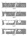
- Fig. 4a relates to a silicon wafer on which the first SiN layer is grown and is patterned on both sides, which yields a cross-section as shown in Fig. 4a : 45 denoting the SiN layer-1 at the upper side, 46 denoting the SiN layer-1 at the lower side, 47 denoting patterned openings in the layer 45 for the SiN tubes 3, 21, and 48 denoting patterned openings in the layer 46 for the fluid coupling to the external world.
- Fig. 2b after the substrate (side 46) has been etched, a cavity 49 is anisotropically etched via openings 48. Note: steps 4b and 4c may be interchanged!
- Fig. 4c after the substrate (side 45) has been etched, cavities 50 are isotropically etched via openings 47. Note again: 4b and 4c may be interchanged!
- Fig. 4d shows the situation after the thicker, second SiN layer has been grown: 51 denoting the SiN layer-2. Everything is covered with the same thickness, also in the various holes. This is also called 'conform deposition'. The deposition of the SiN layer creates a cavity 52.
- Fig. 4e deposition of a metal layer and patterning of this layer 10. This will form the current conductor 10 (cf. Fig. 1 a) on the tube.
- Reference numeral 53 denotes the supply wire for the tube electrode of the sensing capacitors. This electrode 53 lies on the tags 11 located on the tube (cf. Fig. 2a ). This will be discussed in more detail with reference to Fig. 6 .
- Fig. 4f patterning of the (by now dual, 45 + 51) SiN layer at the upper side. If this is omitted, the entire tube 3 will be suspended from a SiN membrane 45 + 51 at the upper side after the final etching step (4j)!
- Reference numeral 54 denotes openings in the upper double SiN layer.
- Fig. 4g providing and patterning of a photoresist layer at the areas of the components of the sensing capacitors, 55 denoting the resist layer that is to serve as a spacer layer.
- Fig. 4h providing and patterning of a second, thicker metal layer.
- the pattern will form the future crossing electrodes at the area of the sensing capacitor, with 56 denoting the patterned electrode, and 42 denoting a layer at the area of the fluid openings for protecting the embedded channels 21.
- Fig. 4i patterning of the lower double SiN layer at side 46, with 57 denoting an opening in the 46 + 51 SiN layer for etching the opening 4.
- Fig. 4j is a cross-sectional view taken on the plane IV j in Fig. 3a : anisotropic KOH etching of the substrate 1 through the mask opening 57 yields this result.
- the tags 11 and 12 now become functional and can be identified.
- the former cavity 52 has now been transformed into the embedded tube 21 and the free tube 3.
- etching of the hole from the side 46 may take place isotropically or anisotropically. Isotropic etching to free the tube 3 may even be done from the 'front', i.e. from side 45 (through the openings 54 in Fig. 4f ), but in that case the etching process must be isotropic.
- Fig. 5a is a plan view showing details of the round bends in the possible tube shapes of a system chip with a Coriolis flow sensor or thermal flow sensor.
- the method according to the invention utilizes a mask for making round bends during the manufacture of the flow tube, the elongate mask openings having a small pitch and extending substantially tangentially.
- tube 21 and tube 3 with rounded corner 23 are shown in FIG. 1 ); substrate 1; free tube 3; current conductor 10 for Lorentz or thermal excitation; tag 11 with sensing capacitor below electrode; transition 20 from embedded tube 21 to free tube 3; embedded tube 21; bend 23 in tube 3 through pattern of openings 47; front 24 of tube 3; fixed wall 27 in which the transitions 20, 20' are located; electrode 53 for sensing capacitors 10 and 53 (both lying in the first metal layer).
- Fig. 5b shows an embodiment in which a number of parallel tubes are joined together into one tube. This is a method of obtaining a lower hydraulic resistance.
- the tubes may be embedded in the substrate, for example, or the same tube structure may be made free in its entirety without a transition 20, i.e. all being of tube type 3 (freely suspended). This may be achieved in that the mask defining the openings of type 54 ( Fig. 4f ) and the mask defining the opening of type 57 ( Fig. 4i ) are correspondingly adapted.
- Figs. 6a and b show two embodiments of the means for capacitive detection of the tube vibrations integrated in a single crystal in more detail.
- the tags are at two levels in the embodiment of Fig. 6a , so that a spacer layer is necessary.
- the tags (the mutually intertwining fingers) are located in one plane, which provides a greater design freedom.
- Fig. 7a shows part of a system chip with a U-shaped Coriolis tube and means for thermal excitation of the tube vibrations, representing a general view of thermal excitation.
- Two independent heater resistors 65, 65' arranged on the legs 22 and 26 of the U-shaped Coriolis tube 3 do and do not heat the legs in alternation. This causes the tube 3 to perform a torsional movement about the axis 29 (so this is unlike the situation of Fig. 2a , where thermal actuation always generates the flapping mode).
- the heater resistor 65 When electric power is dissipated in the heater resistor 65, the temperature in tube portion 22 rises and this portion bends in downward direction.
- the tube When electric power is dissipated in the heater resistor 65', the same happens there. Accordingly, the tube will perform a twisting movement about the axis 29 owing to the alternating dissipation of power in the legs.
- Fig. 7b shows part of a system chip with a U-shaped Coriolis tube 3 suspended at one side of the opening 4 and provided with electrodes 68, 69 for the capacitive read out.
- An additional U-tube 66 suspended at the opposite side of the opening 4 is located straight opposite the U-tube 3 so as to position the finger-shaped electrodes on the tags 68 and 69 exactly at the same z-level.
- the excitation in the case of Fig. 7b may be the same as in Fig. 7a .
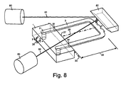
- Fig. 8 shows part of a system chip with Coriolis tube 3 comprising means for optically reading out the movement of the Coriolis tube 3.
- a laser PSD (position sensitive detector) combination measures the translation and rotation of a reflection position on the tube 3 (a metal layer on the tags 11, 11' and 11" also used in the preceding embodiments yields three measuring spots for three laser PSDs).
- laser 80 light beam 81 from laser; mirror 82 oriented at an angle of 45° so as to direct the beam to the tube 3; position sensitive detector 83; beam 84 incident on the PSD after three reflections.
- Fig. 9a shows part of a flowmeter with a system chip and a thermal flow sensor manufactured by means of the technology discussed above.
- the substrate 1 has an opening 4 in which a loop-shaped tube 3 having a U-shape is freely suspended.
- the tube 3 is connected to embedded channels in the substrate 1.
- a heater resistor 91 is arranged in the center of the connecting limb of the free tube 3.
- a thermopile 90 is arranged between the two legs of the free tube 3 for measuring a temperature difference between the legs, which temperature difference is a measure for the flow.
- the U-shaped tube may optionally be fixed by the connecting limb of the U to the wall of the opening 4 opposite thereto.
- Fig. 9b shows an alternative to the embodiment of Fig. 9a .
- the U-shaped free loop of Fig. 9a is transformed into a loop of which two legs 95 and 95' are freely suspended and reach completely across the opening 4, whereas the connecting limb between the two legs is an embedded channel 21 in the substrate 1.
- Heater resistors 94, 94' are provided in the centers of the two legs 95, 95', respectively.
- Thermopiles 93 and 93' are symmetrically arranged between the two legs 95, 95' on either side of the heaters 94, 94'. This makes Fig. 9b a double version of Fig. 9a .
- a thermal flow sensor based on the so-termed TBA principle is also suitable for being manufactured by the above technology.
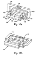
- Figs, 10a and 10b show a system chip 106 with a Coriolis tube 101 and a magnet yoke 100 for Lorentz excitation of the Coriolis tube.
- Fig. 10a shows a loop-shaped (U-shaped in this case) Coriolis tube 101 with the magnet yoke 100 in vertical position (in a plane transverse to the plane of the Coriolis tube 101).
- the magnet yoke 100 for Lorentz excitation in which a permanent magnet is accommodated, is to provide a loop of a soft magnetic material, such as soft iron, that is as fully closed as possible, with air gaps only in those locations where the Coriolis flow tube 101 crosses the path of the loop. A minimum resistance for the magnetic field lines crossing between the poles 102, 102' is realized thereby.
- the preferred embodiment of the magnet yoke 100 is that which comprises not only the C- or U-shaped portion at the outer side of the tube 101, but also a smaller, beam-type part 103 within the loop of the tube 101.
- the beam-type part 103 acts as a flux guide: it draws the fields lines towards itself so that there is no interfering magnetic field acting on locations of the tube outside the air gaps 105, 105'.
- the C- or U-shaped portion is built up from two symmetrical halves between which the permanent magnet 104 is placed.
- the system chip 106 with the Coriolis tube 101 is manufactured from a thin silicon wafer in a number of etching and deposition steps in the 'microchannel' process. This results in a tube that is freely suspended from its inlet and outlet tubes 107, 108 in a silicon frame 109.
- This frame 109 is open at two sides.
- a closed, comparatively flat box is created in that a bottom and lid are glued to the frame 109 in a next manufacturing step.
- This box may be evacuated because a tube vibrating in a vacuum can be kept moving with less energy supplied.
- the lid and/or bottom of the box may be manufactured from a transparent material, such as glass.
- the magnet yoke 100 Before the box is closed, the magnet yoke 100 is placed: the ends of the C-shaped portion of the yoke 100 are glued into recesses of the frame 109 that were etched away during manufacture.
- Fig. 10a shows the stage in the manufacture in which the complete magnet yoke 100 has been put in place, but the lid has not yet been glued over the box.
- the inlet and outlet tubes 107, 108 are shown as issuing into the plane of the frame adjoining the Coriolis tube 101, but they may alternatively lie in the plane of the frame remote from the Coriolis tube 101.
- the Figure shows the preferred embodiment with a flux-guiding soft magnetic body 103 within the loop of the tube 103.
- Fig. 10b shows an embodiment of a system chip 111 with a Coriolis tube 112 wherein a magnet yoke 110 for Lorentz force excitation lies in a plane parallel to the plane of the Coriolis tube 112.
- a conductor pattern or conducting layer (not shown) that is connected to a current source (not shown) so as to pass an alternating current through the tube.
- the invention relates to a fluid and flow measuring system comprising a monocrystalline silicon chip in which a SiN tube has been (partly) etched out and a (freely suspended/standing) SiN tube has been (partly) exposed by etching, with (fluid) bottom connections.
Landscapes
- Physics & Mathematics (AREA)
- Fluid Mechanics (AREA)
- General Physics & Mathematics (AREA)
- Chemical & Material Sciences (AREA)
- Dispersion Chemistry (AREA)
- Measuring Volume Flow (AREA)
- Other Investigation Or Analysis Of Materials By Electrical Means (AREA)
- Silicon Compounds (AREA)
- Crystals, And After-Treatments Of Crystals (AREA)
Abstract
Description
- The invention relates to a flowmeter for measuring the flow of a medium.
- An effective instrument for measuring flows is the Coriolis flowmeter.
- Another category is formed by flowmeters of the thermal type. The invention has for its object to provide a flowmeter and a technology for its manufacture which render possible the measurement of very small flow rates, below 1 g/h, in combination with a universal manufacturing technology that renders it possible to manufacture different types of measuring devices and to integrate them with the additional sensor equipment referred to above.
- The flowmeter according to the invention is for this purpose characterized in that it comprises a system chip with a silicon substrate provided on a carrier, in an opening whereof at least one silicon flow tube is provided for transporting a medium whose flow rate is to be measured, said tube having two ends that merge via a wall of the opening into silicon nitride coated channels in the silicon substrate.
- The invention also relates to a method of manufacturing a system chip for a flowmeter as described above. This method is characterized by the following steps:
- providing a monocrystalline silicon substrate in which a SiN tube is realized by means of SiN deposition steps and partially etching away and partially exposing through etching so as to realize a tube structure that is fixed at at least one side and is otherwise free, by means of micro surface channel technology.
- The invention will be explained in more detail below, by way of example, with reference to the drawing in which:
- Fig. 1 a
- is a diagrammatic elevation of an embodiment of a flowmeter according to the invention with a system chip and a Coriolis flow sensor;
- Fig. 1 b
- is a front elevation of the flowmeter of
Fig. 1 a; - Fig. 1c
- is a cross-sectional view of the flowmeter of
Fig. 1 a; - Fig. 2a
- presents a clarification of the operation of a Coriolis flow sensor in an arrangement with a U-shaped Coriolis tube (with a diagrammatically indicated actuation and sensing of the vibrating Coriolis tube);
- Fig. 2b
- shows a Lorentz actuation (torsion) and capacitive sensing (flapping) of the tube;
- Fig. 2c
- shows a thermal actuation (torsion) and capacitive sensing (flapping) of the tube;
- Fig. 2d
- shows a thermal actuation (flapping, no magnets) and capacitive sensing (torsion);
- Fig. 3a
- shows a detail of the system chip of
Fig. 1 a with a clearly visible pressure sensor of the Pirani type; - Fig. 3b
- is a cross-sectional view of the system chip with fluidic coupling of connection tubes;
- Figs. 4a-j
- are cross-sections through a system chip during manufacture;
- Fig. 5a
- shows details of the manufacture of a round bend in a tube shape;
- Fig. 5b
- shows parallel connections to one tube;
- Figs. 6a and b
- show details of the capacitive detection means of a system chip;
- Fig. 7a
- is an elevation of a system chip with Coriolis tube with thermal excitation means;
- Fig. 7b
- diagrammatically shows a system chip with Coriolis tube with alternative capacitive sensing means;
- Fig. 8
- shows a system chip with Coriolis tube and optical detection means;
- Fig. 9a
- shows a first embodiment of a system chip with a flow sensor of the thermal type;
- Fig. 9b
- shows a second embodiment of a system chip with a flow sensor of the thermal type; and
- Fig. 10
- shows a system chip with Coriolis tube with a magnet yoke for Lorentz force excitation.
- Corresponding components have been given the same reference numerals as much as possible in the Figures.
-
Fig. 1a shows asystem chip 17 comprising amonocrystalline silicon substrate 1 in which anopening 4 has been etched. Thesystem chip 17 in this example has a Coriolis flow sensor with aCoriolis tube 3 of silicon nitride which is freely suspended in theopening 4. In another example the flow sensor may be a thermal flow sensor. In either case anabsolute pressure sensor 2, such as a Pirani pressure sensor, may be integrated in or on thesubstrate 1. The Coriolis tube has a loop shape, in this case a rectangular loop shape. Other loop shapes, such as triangular, trapezoidal, or U-shaped, are also possible. - The
system chip 17 is (monolithically) assembled with two mutually opposedpermanent magnets 9, 9' which are arranged on acarrier 5, for example a PCB (printed circuit board) of ceramic or synthetic resin material with copper tracks thereon. The substrate is manufactured from a <1,0,0> Si wafer mounted on thecarrier 5. The electrical connections between thesystem chip 17 and thecarrier 5 are provided by so-termed bonding wires arranged ingroups 6, 7, and 8. The bonding wires 6 (from and to the sensor chip) serve for conditioning the chip temperature / c.q.temperature control. A local temperature sensor and an (ambient)pressure sensor 2 may be present, if so desired. - The
pressure sensor 2, if present, measures the absolute pressure. This is important because the quality factor of the tube's vibration depends inter alia on the air pressure. - The
bonding wires 7 serve for bringing the freely suspendedtube 3 into vibration. The bonding wires 8 serve for controlling the read-out elements for the freely suspended tube. - The freely suspended
tube 3 together with therod magnets 9, 9', a current conductor (wire) 10 on thetube 3, andcapacitive sensor elements 11 on the tube and 12 on thesystem chip 17 forms a so-termed Coriolis flowmeter, which is further clarified inFigs. 2a to 2c . A body of soft magnetic material may optionally be provided between therod magnets 9 and 9' in a location within the loop so as to enhance the efficiency of the magnet arrangement. - The hydraulic coupling of the
system chip 17 to the external world is provided by pressure blocks 13 and 14 (Fig. 1 b) .Fluid connections 16 and 16' are present in thepressure block 14. The application of a pressure force between thepressure block 13, thesubstrate 1, and thepressure block 14 provides a gastight closure of the fluid connection between thetubes 15, 15' and the substrate 1 (cf.Fig. 3b for more details). -
Fig. 1b shows the same device asFig. 1a , but viewed from the front. The 'upper side' of thesystem chip 17 lies on thecenterline 18 of therod magnets 9 and 9'. -
Fig. 1c shows the same device asFig. 1a , this time taken on a cross-section at the area of the system chip.Bonding wires 7 for the tube actuation control on the PCB from/to the sensor chip are visible, as are bonding wires 8 for the tube sensing control on the PCB from/to the sensor chip. Thebonding wires 6, 7 and 8 thus serve the integrated sensors /transducers of the Coriolis sensor. - A housing may be provided around the entire assembly for protection; this is not shown.
- A pressure measurement of the medium flowing through the tube may also optionally be integrated. A thermal flow measurement of the medium may also be integrated, if so desired.
- Furthermore, an absolute pressure measurement by means of a relative pressure measurement (membrane somewhere in the tube) with respect to the measured absolute ambient pressure is also possible. A complete multiparameter measuring system is thus obtained.
-
Fig. 2a shows aU-shaped Coriolis tube 3 that was made by MST technology, that is freely suspended, and that is partly embedded in the silicon substrate where it merges into inlet and outlet channels present in the substrate and issuing at the side of thesubstrate 1 opposite to the freely suspendedportion 3. The appliedmagnetic field 31 is indicated by arrows B, and the current passed through theconductor 10 on thetube 3 for generating the Lorentz forces is referenced 32. - During operation, a medium enters at 21 and exits at 21'. The mass flow of a medium is the mass that passes through a cross-section of the tube per second. If the mass is a self-contained quantity, the mass flow through the U-tube of
Fig. 2a must be the same everywhere (otherwise mass will accumulate somewhere, or mass disappear somewhere). - Therefore, the mass flow Q has the same (constant) modulus (or vector 'length') everywhere in the
tube 3. However, Q points in the positive x-direction intube portion 22 and in the negative x-direction intube portion 26. - The following methods exist for realizing and applying a Coriolis mass flowmeter with the
U-tube 3 ofFig. 2a : - a torque mode is generated through Lorentz excitation, i.e. a torsional movement (cf.
Fig. 2b ); - heat is generated in the
conductor pattern 10 through thermal excitation, - which leads to a flapping mode (cf.
Fig. 2c ). - The U-tube is actuated (vibrated) about an axis of rotation 29 (= the x-axis), which in the case of a mass flow leads to a Coriolis force in that location where the distance to the axis of rotation changes, which is at
tube portion 24. This Coriolis force ontube portion 24 causes the U-tube 3 to rotate about an axis of rotation 30 (= the y-axis), leading to a translatory movement of thetube portion 24. This (vibratory) actuation movement is referenced 34 inFig. 2b . The resulting Coriolis-induced rotation about the y-axis is proportional to the mass flow and results in a z-movement 35 of thetube portion 24. Thetube portion 24 performs both movements simultaneously, i.e. the actuatingtorsional vibration 34 and the flapping movement 35 (proportional to the mass flow). - The tube is flapped, or actuated (vibrated) about the axis of rotation 30 (= y-axis); this in the case of a mass flow again leads to a Coriolis force in that location where the distance to the axis of rotation changes, which is at tube portion 22 (upward) and tube portion 26 (downward) this time, causing a rotation of the
tube portion 24. The (vibratory) actuation movement of thetube portion 24 in the z-direction is referenced 36 inFig. 2c . The resulting Coriolis-induced rotation about thex-axis 29 is proportional to the mass flow and results in therotational x-movement 37 of thetube portion 24. Again, thetube portion 24 performs both movements simultaneously, i.e. theactuating flapping vibration 36 and thetorsional vibration 37 that is proportional to the mass flow. - Reference numeral 11 (11', 11") in the previous Figures indicates means (projections or tags of SiN) at or on the connecting part between the legs of the
U-shaped tube 3. These form capacitances together with their counterpart means (projections or tags) 12 (12', 12") at the substrate side. This renders it possible to detect the movements of the tube in a capacitive manner. One, two, or three such pairs of tags, for example, may be used. Alternatives will be described below with reference toFigs. 6a and 6b . -
Fig. 2d diagrammatically shows a system chip with thesame U-tube 3 as inFig. 2a , and also suspended in the same manner. In this case, however, the Lorentz actuation is combined with thermal actuation (torsion).Resistance elements legs U-tube 3 when energized. The resistance elements in this case are arranged on projecting (bulging)portions 38, 38' of thesubstrate 1. Upon being energized, each resistance element sends a dynamic heat wave in the z-direction through the respective projecting portion. Adjustment of the energizing currents offers a compensation possibility. -
Fig. 3a shows a detail of the system chip ofFig. 1 a withthick metal layers 42, 42' for guiding the compression force into the main surface of the silicon substrate so as to protect the embedded housings opposite the fluid openings and to leave the SiN membrane exposed. Theintegrated pressure sensor 2 is clearly visible. -
Fig. 3b is a cross-sectional view taken in the plane IV-j inFig. 3a after apressure block 13 has been placed. The fluidic coupling of the connection openings of the system chip (embeddedchannels 40, 40') to an externally appliedfluid tube 16 is clearly visible in this cross-section. The connection is sealed in a gastight manner through plastic deformation of metal rings 42, 43 between the pressure blocks 13, 14 on the one hand and thesilicon substrate 1 on the other. Thepressure block 14 here projects through theopening 15 in thecarrier 5. - The system chip described above is to be regarded as a fluidic PCB (printed circuit board), for which a tube structure having the desired functions is realized in one process in the cleanroom in one substrate. The tube structure according to the invention may be manufactured by means of the so-termed micro surface channel (MST) technology.
- An example of this is the following method:
- a thin, for example 500 nm thick, first silicon nitride layer (SixNy) which is rich in silicon is provided on both sides of a <100> oriented p-type silicon substrate (wafer). Then a 50 nm thick chromium layer is sputtered onto the upper side. This chromium layer is patterned with a photoresist mask having rows of elongate holes (with dimensions of, for example, 6x2 µm), with small interspacings between the holes (for example 2 µm). The pattern in the chromium layer is transferred by means of reactive ion etching (RIE) to the subjacent nitride layer. The channel shape is defined by isotropic plasma etching through the holes in the silicon nitride layer. After the resist mask has been stripped, the chromium mask is removed and a thicker, second SixNy layer is grown to a thickness of approximately 1.4 µm. This will form the channel wall (tube wall) and at the same time seals off the etching holes in the first nitride layer.
- Subsequently, a 10/100 nm layer of chromium/platinum is provided by sputtering and patterned by means of lift-off lithography so as to form the metal track (the electrode) which is necessary for making actuation of the structure possible (for example Lorentz actuation).
- Furthermore, release windows are provided at the lower side of the wafer and fluidic access holes to the tube at the upper side of the wafer by means of RIE etching, and the structure is separated by means of (KOH) wafer through etching.
- A preferred embodiment of the method according to the invention will now be elucidated with reference to
Figs. 4a-j . -
Fig. 4a relates to a silicon wafer on which the first SiN layer is grown and is patterned on both sides, which yields a cross-section as shown inFig. 4a : 45 denoting the SiN layer-1 at the upper side, 46 denoting the SiN layer-1 at the lower side, 47 denoting patterned openings in thelayer 45 for theSiN tubes layer 46 for the fluid coupling to the external world. -
Fig. 2b : after the substrate (side 46) has been etched, a cavity 49 is anisotropically etched viaopenings 48. Note: steps 4b and 4c may be interchanged! -
Fig. 4c : after the substrate (side 45) has been etched,cavities 50 are isotropically etched viaopenings 47. Note again: 4b and 4c may be interchanged! -
Fig. 4d shows the situation after the thicker, second SiN layer has been grown: 51 denoting the SiN layer-2. Everything is covered with the same thickness, also in the various holes. This is also called 'conform deposition'. The deposition of the SiN layer creates acavity 52. -
Fig. 4e : deposition of a metal layer and patterning of thislayer 10. This will form the current conductor 10 (cf.Fig. 1 a) on the tube.Reference numeral 53 denotes the supply wire for the tube electrode of the sensing capacitors. Thiselectrode 53 lies on thetags 11 located on the tube (cf.Fig. 2a ). This will be discussed in more detail with reference toFig. 6 . -
Fig. 4f : patterning of the (by now dual, 45 + 51) SiN layer at the upper side. If this is omitted, theentire tube 3 will be suspended from aSiN membrane 45 + 51 at the upper side after the final etching step (4j)!Reference numeral 54 denotes openings in the upper double SiN layer. -
Fig. 4g : providing and patterning of a photoresist layer at the areas of the components of the sensing capacitors, 55 denoting the resist layer that is to serve as a spacer layer. -
Fig. 4h : providing and patterning of a second, thicker metal layer. The pattern will form the future crossing electrodes at the area of the sensing capacitor, with 56 denoting the patterned electrode, and 42 denoting a layer at the area of the fluid openings for protecting the embeddedchannels 21. -
Fig. 4i : patterning of the lower double SiN layer atside 46, with 57 denoting an opening in the 46 + 51 SiN layer for etching theopening 4. -
Fig. 4j is a cross-sectional view taken on the plane IV j inFig. 3a : anisotropic KOH etching of thesubstrate 1 through themask opening 57 yields this result. Thetags former cavity 52 has now been transformed into the embeddedtube 21 and thefree tube 3. Note that etching of the hole from theside 46 may take place isotropically or anisotropically. Isotropic etching to free thetube 3 may even be done from the 'front', i.e. from side 45 (through theopenings 54 inFig. 4f ), but in that case the etching process must be isotropic. -
- A) Provision of a first SiN layer on both sides of the silicon wafer. The upper side is patterned with the tube structure, the lower side with the holes to be etched.
- B) Etching of a hole into the lower side of the wafer to a depth greater than the wafer thickness minus the desired tube thickness.
- C) Isotropic etching through the free holes at the upper side: the tube is defined. The longer the etching, the thicker the tube will be.
- D) Deposition of the second, thicker SiN layer in an LPCVD tubular oven.
All wetted materials thus become SiN. - E) Deposition and patterning of the first metal layer (conductor pattern).
- F) Exposing the upper side of the Coriolis tube (at two or three sides).
- G) Applying a photoresist layer that is to serve as a spacer for the capacitive read-out.
- H) Providing and patterning the second, thicker metal layer. This layer also serves as an intermediate layer for the pressure blocks 13 (cf.
Fig. 1 ). - I) Providing the etching mask for exposing the Coriolis tube through etching.
- J) Separating the chip from the wafer by sawing or breaking off. This is facilitated in that the holes are covered by sawing foil at the lower side.
-
Fig. 5a is a plan view showing details of the round bends in the possible tube shapes of a system chip with a Coriolis flow sensor or thermal flow sensor. The method according to the invention utilizes a mask for making round bends during the manufacture of the flow tube, the elongate mask openings having a small pitch and extending substantially tangentially. - Visible are: detail of
tube 21 andtube 3 with rounded corner 23 (cf.Fig. 2a );substrate 1;free tube 3;current conductor 10 for Lorentz or thermal excitation;tag 11 with sensing capacitor below electrode;transition 20 from embeddedtube 21 tofree tube 3; embeddedtube 21;bend 23 intube 3 through pattern ofopenings 47;front 24 oftube 3; fixedwall 27 in which thetransitions 20, 20' are located;electrode 53 for sensingcapacitors 10 and 53 (both lying in the first metal layer). -
Fig. 5b shows an embodiment in which a number of parallel tubes are joined together into one tube. This is a method of obtaining a lower hydraulic resistance. The tubes may be embedded in the substrate, for example, or the same tube structure may be made free in its entirety without atransition 20, i.e. all being of tube type 3 (freely suspended). This may be achieved in that the mask defining the openings of type 54 (Fig. 4f ) and the mask defining the opening of type 57 (Fig. 4i ) are correspondingly adapted. -
Figs. 6a and b show two embodiments of the means for capacitive detection of the tube vibrations integrated in a single crystal in more detail. Detail oftube 3,front side 24, with electrodes for capacitive read out, showing: -
substrate 1;front 2 of free tube;current conductor 10 for Lorentz or thermal excitation;tag 11 attube 3; tag 12 at opposite side ofsubstrate 1;tube electrode 53 of sensing capacitors;electrodes 60 made in second metal layer;bond pad 61;finger electrode 62 at the substrate side;finger electrode 63 at the tube side. - The tags are at two levels in the embodiment of
Fig. 6a , so that a spacer layer is necessary. In the embodiment ofFig. 6b , the tags (the mutually intertwining fingers) are located in one plane, which provides a greater design freedom. -
Fig. 7a shows part of a system chip with a U-shaped Coriolis tube and means for thermal excitation of the tube vibrations, representing a general view of thermal excitation. Twoindependent heater resistors 65, 65' arranged on thelegs U-shaped Coriolis tube 3 do and do not heat the legs in alternation. This causes thetube 3 to perform a torsional movement about the axis 29 (so this is unlike the situation ofFig. 2a , where thermal actuation always generates the flapping mode). When electric power is dissipated in theheater resistor 65, the temperature intube portion 22 rises and this portion bends in downward direction. - When electric power is dissipated in the heater resistor 65', the same happens there. Accordingly, the tube will perform a twisting movement about the
axis 29 owing to the alternating dissipation of power in the legs. -
Fig. 7b shows part of a system chip with aU-shaped Coriolis tube 3 suspended at one side of theopening 4 and provided withelectrodes additional U-tube 66 suspended at the opposite side of theopening 4 is located straight opposite theU-tube 3 so as to position the finger-shaped electrodes on thetags Fig. 7b may be the same as inFig. 7a . -
Fig. 8 shows part of a system chip withCoriolis tube 3 comprising means for optically reading out the movement of theCoriolis tube 3. A laser PSD (position sensitive detector) combination measures the translation and rotation of a reflection position on the tube 3 (a metal layer on thetags - Visible are:
laser 80;light beam 81 from laser;mirror 82 oriented at an angle of 45° so as to direct the beam to thetube 3; positionsensitive detector 83;beam 84 incident on the PSD after three reflections. -
Fig. 9a shows part of a flowmeter with a system chip and a thermal flow sensor manufactured by means of the technology discussed above. Thesubstrate 1 has anopening 4 in which a loop-shapedtube 3 having a U-shape is freely suspended. Thetube 3 is connected to embedded channels in thesubstrate 1. Aheater resistor 91 is arranged in the center of the connecting limb of thefree tube 3. Athermopile 90 is arranged between the two legs of thefree tube 3 for measuring a temperature difference between the legs, which temperature difference is a measure for the flow. The U-shaped tube may optionally be fixed by the connecting limb of the U to the wall of theopening 4 opposite thereto. - All this is arranged such that the flowmeter operates in accordance with the thermal flow sensor principle disclosed in
EP 774 649 -
Fig. 9b shows an alternative to the embodiment ofFig. 9a . The U-shaped free loop ofFig. 9a is transformed into a loop of which twolegs 95 and 95' are freely suspended and reach completely across theopening 4, whereas the connecting limb between the two legs is an embeddedchannel 21 in thesubstrate 1.Heater resistors 94, 94' are provided in the centers of the twolegs 95, 95', respectively. Thermopiles 93 and 93' are symmetrically arranged between the twolegs 95, 95' on either side of theheaters 94, 94'. This makesFig. 9b a double version ofFig. 9a . - A thermal flow sensor based on the so-termed TBA principle is also suitable for being manufactured by the above technology.
- Magnet yoke for Lorentz excitation (so-termed torque excitation):
- The Lorentz excitation may be achieved in an alternative manner by means of a magnet yoke instead of the two permanent magnets.
Figs, 10a and 10b show asystem chip 106 with aCoriolis tube 101 and amagnet yoke 100 for Lorentz excitation of the Coriolis tube.Fig. 10a shows a loop-shaped (U-shaped in this case)Coriolis tube 101 with themagnet yoke 100 in vertical position (in a plane transverse to the plane of the Coriolis tube 101). - Description of embodiment with system chip in Micro System Technology (MST): The
magnet yoke 100 for Lorentz excitation, in which a permanent magnet is accommodated, is to provide a loop of a soft magnetic material, such as soft iron, that is as fully closed as possible, with air gaps only in those locations where theCoriolis flow tube 101 crosses the path of the loop. A minimum resistance for the magnetic field lines crossing between thepoles 102, 102' is realized thereby. The preferred embodiment of themagnet yoke 100 is that which comprises not only the C- or U-shaped portion at the outer side of thetube 101, but also a smaller, beam-type part 103 within the loop of thetube 101. Said part shortens the path to be crossed by the field lines and thus reduces the magnetic resistance, so that a smaller magnet and/or a weaker current through a conducting layer on thetube 101 can suffice for realizing a given Lorentz force. In addition, the beam-type part 103 acts as a flux guide: it draws the fields lines towards itself so that there is no interfering magnetic field acting on locations of the tube outside theair gaps 105, 105'. The C- or U-shaped portion is built up from two symmetrical halves between which thepermanent magnet 104 is placed. - The
system chip 106 with theCoriolis tube 101 is manufactured from a thin silicon wafer in a number of etching and deposition steps in the 'microchannel' process. This results in a tube that is freely suspended from its inlet andoutlet tubes silicon frame 109. Thisframe 109 is open at two sides. A closed, comparatively flat box is created in that a bottom and lid are glued to theframe 109 in a next manufacturing step. This box may be evacuated because a tube vibrating in a vacuum can be kept moving with less energy supplied. In the case of an optical measurement of the displacement of thetube 101, with a light source and detector located outside the box, the lid and/or bottom of the box may be manufactured from a transparent material, such as glass. - Before the box is closed, the
magnet yoke 100 is placed: the ends of the C-shaped portion of theyoke 100 are glued into recesses of theframe 109 that were etched away during manufacture. The beam-type part 103 of the yoke, which lies within the loop of thetube 101, is glued to the bottom of the box before or after this bottom is glued to theframe 109. -
Fig. 10a shows the stage in the manufacture in which thecomplete magnet yoke 100 has been put in place, but the lid has not yet been glued over the box. The inlet andoutlet tubes Coriolis tube 101, but they may alternatively lie in the plane of the frame remote from theCoriolis tube 101. The Figure shows the preferred embodiment with a flux-guiding softmagnetic body 103 within the loop of thetube 103. -
Fig. 10b shows an embodiment of asystem chip 111 with aCoriolis tube 112 wherein amagnet yoke 110 for Lorentz force excitation lies in a plane parallel to the plane of theCoriolis tube 112. In both cases it is necessary for the generation of the Lorentz forces that theCoriolis tube - It is noted that the embodiments of Lorentz actuation and thermal actuation, with optical or capacitive sensing as described above may also be used in other embodiments of flowmeters with flow tubes manufactured by means of MST, for example the Coriolis flowmeter described in
US 6,477,901 . - Summarizing, the invention relates to a fluid and flow measuring system comprising a monocrystalline silicon chip in which a SiN tube has been (partly) etched out and a (freely suspended/standing) SiN tube has been (partly) exposed by etching, with (fluid) bottom connections.
Claims (20)
- A flowmeter with a system chip comprising a silicon substrate provided on a carrier, in an opening whereof at least one silicon flow tube is provided for transporting a medium whose flow rate is to be measured, said tube having two ends that issue via a wall of the opening into silicon nitride coated channels in the silicon substrate.
- A flowmeter as claimed in claim 1,
characterized in that the channels are connected through the carrier to connecting lines to the external world. - A flowmeter as claimed in claim 1,
wherein the flow tube has a loop shape and lies free from the walls of the opening at three sides. - A flowmeter as claimed in claim 1,
comprising means (A) for vibrating the tube and means (B) for detecting the movement of the tube. - A flowmeter as claimed in claim 4,
wherein the means (A) comprise a conductor pattern on the flow tube, means for passing an alternating current through the conductor pattern, and means for generating a permanent magnetic field at the area of the flow tube. - A flowmeter as claimed in claim 4,
wherein the means (A) excite the flow tube thermally. - A flowmeter as claimed in claim 4,
wherein the means (A) operate through heating and cooling of the bimorph formed by the tube and the conductor pattern provided thereon. - A flowmeter as claimed in claim 5,
wherein the means (B) operate capacitively, the conductor pattern acting as one plate of a capacitor. - A flowmeter as claimed in claim 5,
wherein the means (B) operate optically, a light beam being directed at the conductor pattern and the reflected light being detected. - A flowmeter as claimed in claim 1,
wherein the flow tube is U-shaped, lies free from the wall of the opening at three sides, and is associated with a thermopile that is arranged so as to measure a temperature difference between the legs of the U. - A method of manufacturing a system chip for a flowmeter, wherein a monocrystalline silicon substrate is provided in which a SiN tube is realized by means of SiN deposition steps and partially etching out and partially exposing by etching, such that a tube structure is realized that is fixed at at least one side and is otherwise free, for which a micro surface channel technology is used.
- A method as claimed in claim 11,
wherein the substrate has two mutually opposed main surfaces, the freely suspended tube structure adjoins one of the main surfaces, and one or more tube connections to the external world is or are provided in the other main surface. - A method as claimed in claim 11,
characterized by the following steps:A) A1. Providing a silicon substrate (wafer).A2. Providing a first SiN layer on both sides of the silicon wafer. The upper side is patterned with the tube structure (pattern of elongate holes), the lower side with the connecting holes that are to be etched.B) Etching of a hole into the lower side of the wafer for each tube connection to a depth greater than the wafer thickness minus the desired tube thickness.C) Isotropic etching through the free holes at the upper side so as to define the tube during a period of time necessary for realizing a predetermined tube diameter.D) Deposition of a second SiN layer.E) Providing and patterning of a first metal layer (conductor pattern).F) Exposing the tube at two or three sides at the upper side.G) (Optional) Applying a thick photoresist layer that is to serve as a spacer.H) Providing and patterning a second metal layer.I) Providing an etching mask for exposing the tube through etching, for example in an isotropic or anisotropic etching process.J) Separating the chip from the wafer. - A method as claimed in claim 11,
wherein a loop-shaped flow tube with rounded corners is realized. - A method as claimed in claim 11,
wherein in one and the same process also an electronic sensor structure is integrated in/on the substrate. - A method as claimed in claim 11,
wherein the electronic sensor structure comprises a pressure sensor. - A method as claimed in claim 11,
wherein the pressure sensor is a Pirani pressure sensor. - A flowmeter as claimed in claim 1,
characterized in that the silicon nitride flow tube forms part of a Coriolis flow sensor or of a thermal flow sensor. - A flowmeter as claimed in claim 1,
characterized by a first silicon nitride flow tube for a Coriolis flow sensor and a second silicon nitride flow tube for a thermal flow sensor. - A flowmeter as claimed in claim 1,
characterized in that the flow tube forms part of a Coriolis flow sensor, and in that Lorentz excitation means are present for exciting the Coriolis tube as well as additional excitation means.
Applications Claiming Priority (1)
| Application Number | Priority Date | Filing Date | Title |
|---|---|---|---|
| NL1034905A NL1034905C2 (en) | 2008-01-11 | 2008-01-11 | Flow measuring device. |
Publications (2)
| Publication Number | Publication Date |
|---|---|
| EP2078936A1 true EP2078936A1 (en) | 2009-07-15 |
| EP2078936B1 EP2078936B1 (en) | 2011-02-09 |
Family
ID=39638767
Family Applications (1)
| Application Number | Title | Priority Date | Filing Date |
|---|---|---|---|
| EP08075910A Active EP2078936B1 (en) | 2008-01-11 | 2008-12-02 | Flowmeter with silicon flow tube |
Country Status (8)
| Country | Link |
|---|---|
| US (1) | US7895905B2 (en) |
| EP (1) | EP2078936B1 (en) |
| JP (1) | JP5537025B2 (en) |
| AT (1) | ATE498117T1 (en) |
| DE (1) | DE602008004881D1 (en) |
| DK (1) | DK2078936T3 (en) |
| ES (1) | ES2358161T3 (en) |
| NL (1) | NL1034905C2 (en) |
Cited By (11)
| Publication number | Priority date | Publication date | Assignee | Title |
|---|---|---|---|---|
| NL2006895C2 (en) * | 2011-06-03 | 2012-12-04 | Berkin Bv | FLOW MEASURING DEVICE AND ITS USE FOR DETERMINING A FLOW OF A MEDIA, AND THE METHOD FOR THIS. |
| WO2014104889A1 (en) | 2012-12-27 | 2014-07-03 | Berkin B.V. | Device and method for determining the combustion value of a fuel |
| NL2010798C2 (en) * | 2013-05-14 | 2014-11-24 | Berkin Bv | FLOW MEASURING DEVICE FOR MEASURING A FLOW OF A MEDIUM. |
| WO2017123089A1 (en) * | 2016-01-14 | 2017-07-20 | Berkin B.V. | Coriolis flowsensor |
| EP3298441B1 (en) * | 2015-05-20 | 2019-03-13 | Signify Holding B.V. | Lighting device, lens and method |
| WO2019054873A1 (en) | 2017-09-15 | 2019-03-21 | Berkin B.V. | Method of fabricating a micro machined channel |
| WO2019143239A1 (en) | 2018-01-18 | 2019-07-25 | Berkin B.V. | Coriolis flow sensor |
| NL2020298B1 (en) * | 2018-01-19 | 2019-07-29 | Berkin Bv | Coriolis flowsensor |
| WO2020178002A1 (en) * | 2019-03-07 | 2020-09-10 | Endress+Hauser Flowtec Ag | Coriolis sensor and coriolis measuring device having a coriolis sensor |
| NL2023872B1 (en) | 2019-09-20 | 2021-05-27 | Berkin Bv | Microelectromechanical system component comprising a free-hanging or free-standing microchannel |
| US20210310920A1 (en) * | 2018-08-08 | 2021-10-07 | Endress+Hauser Flowtec Ag | Measuring transducer and measurement device |
Families Citing this family (12)
| Publication number | Priority date | Publication date | Assignee | Title |
|---|---|---|---|---|
| DE102006029443B3 (en) * | 2006-06-21 | 2008-01-31 | Siemens Ag | Sensor in micromechanical design for measuring the mass flow rate according to the Coriolis principle |
| US9072464B2 (en) * | 2009-07-22 | 2015-07-07 | Koninklijke Philips N.V. | Thermal flow sensor integrated circuit with low response time and high sensitivity |
| DE102009046839A1 (en) * | 2009-11-18 | 2011-05-19 | Endress + Hauser Flowtec Ag | Measuring system with a two parallel flowed measuring tubes having pipe assembly and method for monitoring thereof |
| JP2012247372A (en) * | 2011-05-30 | 2012-12-13 | Nippon Mektron Ltd | Pressure sensor, manufacturing method thereof, and pressure detection module |
| DE102011114506A1 (en) * | 2011-09-22 | 2013-03-28 | Technische Universität Ilmenau | Method and device for non-contact measurement of a mass or volume flow of an electrically conductive fluid |
| US9151652B2 (en) | 2013-09-20 | 2015-10-06 | Teledyne Instruments, Inc. | Coriolis flow sensor fabricated with laminated films processes |
| US20160202101A1 (en) * | 2015-01-12 | 2016-07-14 | Douglas Ray Sparks | Sensor structures and methods of forming using three-dimensional printing techniques |
| DE102016104551B4 (en) * | 2016-03-11 | 2025-04-03 | Krohne AG | Procedure for equipping a Coriolis mass flowmeter with electrical connections |
| US10409295B2 (en) * | 2016-12-31 | 2019-09-10 | Applied Materials, Inc. | Methods and apparatus for enhanced flow detection repeatability of thermal-based mass flow controllers (MFCS) |
| WO2020198318A1 (en) * | 2019-03-25 | 2020-10-01 | Flo Technologies, Inc. | Thin film thermal mass flow sensors in fluid applications |
| US11262226B2 (en) * | 2020-02-17 | 2022-03-01 | GWU Design | Hybrid mass flow sensor including a thermal and coriolis principle measurement arrangements |
| NL2028203B1 (en) * | 2021-05-12 | 2022-12-08 | Berkin Bv | Device for controlling or measuring a fluid |
Citations (5)
| Publication number | Priority date | Publication date | Assignee | Title |
|---|---|---|---|---|
| EP0774649A1 (en) | 1995-11-17 | 1997-05-21 | Berkin B.V. | Flow meter |
| US6477901B1 (en) | 1999-12-21 | 2002-11-12 | Integrated Sensing Systems, Inc. | Micromachined fluidic apparatus |
| EP1291621A1 (en) * | 2000-05-19 | 2003-03-12 | Mitsubishi Denki Kabushiki Kaisha | Heat-sensitive type flow rate detecting element and holder therefor |
| US20060037187A1 (en) * | 2004-08-20 | 2006-02-23 | Integrated Sensing Systems, Inc. | Process of making a microtube and microfluidic devices formed therewith |
| WO2007147786A1 (en) * | 2006-06-21 | 2007-12-27 | Siemens Aktiengesellschaft | Micromechanical sensor for measuring the mass flow rate in accordance with the coriolis principle |
Family Cites Families (6)
| Publication number | Priority date | Publication date | Assignee | Title |
|---|---|---|---|---|
| JPS58165623U (en) * | 1982-04-13 | 1983-11-04 | 横河電機株式会社 | mass flow meter |
| JPS59105522A (en) * | 1982-12-08 | 1984-06-18 | Horiba Ltd | Flow rate sensor and manufacture thereof |
| US5233213A (en) * | 1990-07-14 | 1993-08-03 | Robert Bosch Gmbh | Silicon-mass angular acceleration sensor |
| NL1028938C2 (en) * | 2005-05-02 | 2006-11-03 | Berkin Bv | Mass flow meter of the Coriolist type. |
| NL1028939C2 (en) * | 2005-05-02 | 2006-11-03 | Berkin Bv | Mass flow meter of the Coriolist type. |
| WO2007136069A1 (en) * | 2006-05-22 | 2007-11-29 | Kazumasa Ohnishi | Coriolis flowmeter |
-
2008
- 2008-01-11 NL NL1034905A patent/NL1034905C2/en not_active IP Right Cessation
- 2008-12-02 ES ES08075910T patent/ES2358161T3/en active Active
- 2008-12-02 DE DE602008004881T patent/DE602008004881D1/en active Active
- 2008-12-02 AT AT08075910T patent/ATE498117T1/en active
- 2008-12-02 EP EP08075910A patent/EP2078936B1/en active Active
- 2008-12-02 DK DK08075910.3T patent/DK2078936T3/en active
- 2008-12-15 US US12/335,045 patent/US7895905B2/en active Active
- 2008-12-26 JP JP2008331938A patent/JP5537025B2/en active Active
Patent Citations (5)
| Publication number | Priority date | Publication date | Assignee | Title |
|---|---|---|---|---|
| EP0774649A1 (en) | 1995-11-17 | 1997-05-21 | Berkin B.V. | Flow meter |
| US6477901B1 (en) | 1999-12-21 | 2002-11-12 | Integrated Sensing Systems, Inc. | Micromachined fluidic apparatus |
| EP1291621A1 (en) * | 2000-05-19 | 2003-03-12 | Mitsubishi Denki Kabushiki Kaisha | Heat-sensitive type flow rate detecting element and holder therefor |
| US20060037187A1 (en) * | 2004-08-20 | 2006-02-23 | Integrated Sensing Systems, Inc. | Process of making a microtube and microfluidic devices formed therewith |
| WO2007147786A1 (en) * | 2006-06-21 | 2007-12-27 | Siemens Aktiengesellschaft | Micromechanical sensor for measuring the mass flow rate in accordance with the coriolis principle |
Non-Patent Citations (1)
| Title |
|---|
| PETER ENOKSSON ET AL: "A Silicon Resonant Sensor Structure for Coriolis Mass-Flow Measurements", JOURNAL OF MICROELECTROMECHANICAL SYSTEMS, IEEE SERVICE CENTER, PISCATAWAY, NJ, US, vol. 6, no. 2, 1 June 1997 (1997-06-01), XP011034742, ISSN: 1057-7157 * |
Cited By (20)
| Publication number | Priority date | Publication date | Assignee | Title |
|---|---|---|---|---|
| EP2530438A1 (en) | 2011-06-03 | 2012-12-05 | Berkin B.V. | Flow measurement device and its use |
| US8881601B2 (en) | 2011-06-03 | 2014-11-11 | Berkin B.V. | Flow meter and use thereof for determining a flow of a medium, as well as a method therefor |
| NL2006895C2 (en) * | 2011-06-03 | 2012-12-04 | Berkin Bv | FLOW MEASURING DEVICE AND ITS USE FOR DETERMINING A FLOW OF A MEDIA, AND THE METHOD FOR THIS. |
| CN105026920B (en) * | 2012-12-27 | 2018-07-31 | 伯金有限公司 | Device and method for determining the combustion value of a fuel |
| WO2014104889A1 (en) | 2012-12-27 | 2014-07-03 | Berkin B.V. | Device and method for determining the combustion value of a fuel |
| CN105026920A (en) * | 2012-12-27 | 2015-11-04 | 伯金有限公司 | Device and method for determining the combustion value of a fuel |
| US9857321B2 (en) | 2012-12-27 | 2018-01-02 | Berkin B.V. | Device and method for determining the combustion value of a fuel |
| NL2010798C2 (en) * | 2013-05-14 | 2014-11-24 | Berkin Bv | FLOW MEASURING DEVICE FOR MEASURING A FLOW OF A MEDIUM. |
| EP3298441B1 (en) * | 2015-05-20 | 2019-03-13 | Signify Holding B.V. | Lighting device, lens and method |
| KR20180108663A (en) * | 2016-01-14 | 2018-10-04 | 버킨 비.브이. | Coriolis flow sensor |
| NL2016092B1 (en) * | 2016-01-14 | 2017-07-24 | Berkin Bv | Coriolis flowsensor. |
| WO2017123089A1 (en) * | 2016-01-14 | 2017-07-20 | Berkin B.V. | Coriolis flowsensor |
| US10627277B2 (en) | 2016-01-14 | 2020-04-21 | Berkin B.V. | Coriolis flow sensor having two detection elements partly overlapping the excitation axis and arranged on opposite sides of the flow tube |
| WO2019054873A1 (en) | 2017-09-15 | 2019-03-21 | Berkin B.V. | Method of fabricating a micro machined channel |
| WO2019143239A1 (en) | 2018-01-18 | 2019-07-25 | Berkin B.V. | Coriolis flow sensor |
| NL2020298B1 (en) * | 2018-01-19 | 2019-07-29 | Berkin Bv | Coriolis flowsensor |
| US20210310920A1 (en) * | 2018-08-08 | 2021-10-07 | Endress+Hauser Flowtec Ag | Measuring transducer and measurement device |
| US11933806B2 (en) * | 2018-08-08 | 2024-03-19 | Endress+Hauser Flowtec Ag | Measuring transducer and measurement device |
| WO2020178002A1 (en) * | 2019-03-07 | 2020-09-10 | Endress+Hauser Flowtec Ag | Coriolis sensor and coriolis measuring device having a coriolis sensor |
| NL2023872B1 (en) | 2019-09-20 | 2021-05-27 | Berkin Bv | Microelectromechanical system component comprising a free-hanging or free-standing microchannel |
Also Published As
| Publication number | Publication date |
|---|---|
| US20090308177A1 (en) | 2009-12-17 |
| EP2078936B1 (en) | 2011-02-09 |
| DE602008004881D1 (en) | 2011-03-24 |
| ES2358161T3 (en) | 2011-05-06 |
| DK2078936T3 (en) | 2011-04-18 |
| JP2009168805A (en) | 2009-07-30 |
| ATE498117T1 (en) | 2011-02-15 |
| US7895905B2 (en) | 2011-03-01 |
| NL1034905C2 (en) | 2009-07-14 |
| JP5537025B2 (en) | 2014-07-02 |
Similar Documents
| Publication | Publication Date | Title |
|---|---|---|
| EP2078936B1 (en) | Flowmeter with silicon flow tube | |
| CN101952193B (en) | Microfluidic devices and operations and methods of making the same | |
| US6935010B2 (en) | Method of fabricating a micromachined tube for fluid flow | |
| Ebefors et al. | Three dimensional silicon triple-hot-wire anemometer based on polyimide joints | |
| CN101970338B (en) | Microfluidic device and method of operation | |
| JP4082907B2 (en) | Vibration type pressure sensor | |
| US8695418B2 (en) | Fluidic systems and methods of determining properties of fluids flowing therein | |
| JP6771036B2 (en) | Coriolis flow meter | |
| US20150114137A1 (en) | Apparatus and methods for density and mass flow sensing with a micromachined dual-tube resonator | |
| US6784381B2 (en) | Method of manufacturing a microbalance | |
| WO2008057911A2 (en) | Microelectronic flow sensor packaging method and system | |
| JPH11201788A (en) | Semiconductor Karman vortex flow sensor and method of manufacturing the same | |
| WO2019143239A1 (en) | Coriolis flow sensor | |
| Arslan | MEMS electro thermal actuators: modeling and simulation | |
| CN116625346A (en) | An independent sensitive MEMS thermal expansion flow gyroscope | |
| CN121134673A (en) | A method for manufacturing a MEMS packaging structure | |
| JPH05333036A (en) | Flow sensor | |
| BRPI0103431B1 (en) | CORIOLIS MASS FLOW SENSOR |
Legal Events
| Date | Code | Title | Description |
|---|---|---|---|
| PUAI | Public reference made under article 153(3) epc to a published international application that has entered the european phase |
Free format text: ORIGINAL CODE: 0009012 |
|
| AK | Designated contracting states |
Kind code of ref document: A1 Designated state(s): AT BE BG CH CY CZ DE DK EE ES FI FR GB GR HR HU IE IS IT LI LT LU LV MC MT NL NO PL PT RO SE SI SK TR |
|
| AX | Request for extension of the european patent |
Extension state: AL BA MK RS |
|
| 17P | Request for examination filed |
Effective date: 20091207 |
|
| AKX | Designation fees paid |
Designated state(s): AT BE BG CH CY CZ DE DK EE ES FI FR GB GR HR HU IE IS IT LI LT LU LV MC MT NL NO PL PT RO SE SI SK TR |
|
| 17Q | First examination report despatched |
Effective date: 20100316 |
|
| GRAP | Despatch of communication of intention to grant a patent |
Free format text: ORIGINAL CODE: EPIDOSNIGR1 |
|
| GRAS | Grant fee paid |
Free format text: ORIGINAL CODE: EPIDOSNIGR3 |
|
| GRAA | (expected) grant |
Free format text: ORIGINAL CODE: 0009210 |
|
| AK | Designated contracting states |
Kind code of ref document: B1 Designated state(s): AT BE BG CH CY CZ DE DK EE ES FI FR GB GR HR HU IE IS IT LI LT LU LV MC MT NL NO PL PT RO SE SI SK TR |
|
| REG | Reference to a national code |
Ref country code: GB Ref legal event code: FG4D |
|
| REG | Reference to a national code |
Ref country code: CH Ref legal event code: EP |
|
| REG | Reference to a national code |
Ref country code: CH Ref legal event code: NV Representative=s name: ISLER & PEDRAZZINI AG |
|
| REG | Reference to a national code |
Ref country code: IE Ref legal event code: FG4D |
|
| REF | Corresponds to: |
Ref document number: 602008004881 Country of ref document: DE Date of ref document: 20110324 Kind code of ref document: P |
|
| REG | Reference to a national code |
Ref country code: DE Ref legal event code: R096 Ref document number: 602008004881 Country of ref document: DE Effective date: 20110324 |
|
| REG | Reference to a national code |
Ref country code: NL Ref legal event code: T3 |
|
| REG | Reference to a national code |
Ref country code: SE Ref legal event code: TRGR |
|
| REG | Reference to a national code |
Ref country code: DK Ref legal event code: T3 |
|
| REG | Reference to a national code |
Ref country code: ES Ref legal event code: FG2A Ref document number: 2358161 Country of ref document: ES Kind code of ref document: T3 Effective date: 20110425 |
|
| LTIE | Lt: invalidation of european patent or patent extension |
Effective date: 20110209 |
|
| PG25 | Lapsed in a contracting state [announced via postgrant information from national office to epo] |
Ref country code: NO Free format text: LAPSE BECAUSE OF FAILURE TO SUBMIT A TRANSLATION OF THE DESCRIPTION OR TO PAY THE FEE WITHIN THE PRESCRIBED TIME-LIMIT Effective date: 20110509 Ref country code: LV Free format text: LAPSE BECAUSE OF FAILURE TO SUBMIT A TRANSLATION OF THE DESCRIPTION OR TO PAY THE FEE WITHIN THE PRESCRIBED TIME-LIMIT Effective date: 20110209 Ref country code: PT Free format text: LAPSE BECAUSE OF FAILURE TO SUBMIT A TRANSLATION OF THE DESCRIPTION OR TO PAY THE FEE WITHIN THE PRESCRIBED TIME-LIMIT Effective date: 20110609 Ref country code: LT Free format text: LAPSE BECAUSE OF FAILURE TO SUBMIT A TRANSLATION OF THE DESCRIPTION OR TO PAY THE FEE WITHIN THE PRESCRIBED TIME-LIMIT Effective date: 20110209 Ref country code: GR Free format text: LAPSE BECAUSE OF FAILURE TO SUBMIT A TRANSLATION OF THE DESCRIPTION OR TO PAY THE FEE WITHIN THE PRESCRIBED TIME-LIMIT Effective date: 20110510 Ref country code: HR Free format text: LAPSE BECAUSE OF FAILURE TO SUBMIT A TRANSLATION OF THE DESCRIPTION OR TO PAY THE FEE WITHIN THE PRESCRIBED TIME-LIMIT Effective date: 20110209 |
|
| PG25 | Lapsed in a contracting state [announced via postgrant information from national office to epo] |
Ref country code: BG Free format text: LAPSE BECAUSE OF FAILURE TO SUBMIT A TRANSLATION OF THE DESCRIPTION OR TO PAY THE FEE WITHIN THE PRESCRIBED TIME-LIMIT Effective date: 20110509 Ref country code: SI Free format text: LAPSE BECAUSE OF FAILURE TO SUBMIT A TRANSLATION OF THE DESCRIPTION OR TO PAY THE FEE WITHIN THE PRESCRIBED TIME-LIMIT Effective date: 20110209 Ref country code: CY Free format text: LAPSE BECAUSE OF FAILURE TO SUBMIT A TRANSLATION OF THE DESCRIPTION OR TO PAY THE FEE WITHIN THE PRESCRIBED TIME-LIMIT Effective date: 20110209 Ref country code: FI Free format text: LAPSE BECAUSE OF FAILURE TO SUBMIT A TRANSLATION OF THE DESCRIPTION OR TO PAY THE FEE WITHIN THE PRESCRIBED TIME-LIMIT Effective date: 20110209 Ref country code: PL Free format text: LAPSE BECAUSE OF FAILURE TO SUBMIT A TRANSLATION OF THE DESCRIPTION OR TO PAY THE FEE WITHIN THE PRESCRIBED TIME-LIMIT Effective date: 20110209 |
|
| PG25 | Lapsed in a contracting state [announced via postgrant information from national office to epo] |
Ref country code: EE Free format text: LAPSE BECAUSE OF FAILURE TO SUBMIT A TRANSLATION OF THE DESCRIPTION OR TO PAY THE FEE WITHIN THE PRESCRIBED TIME-LIMIT Effective date: 20110209 |
|
| PG25 | Lapsed in a contracting state [announced via postgrant information from national office to epo] |
Ref country code: CZ Free format text: LAPSE BECAUSE OF FAILURE TO SUBMIT A TRANSLATION OF THE DESCRIPTION OR TO PAY THE FEE WITHIN THE PRESCRIBED TIME-LIMIT Effective date: 20110209 Ref country code: RO Free format text: LAPSE BECAUSE OF FAILURE TO SUBMIT A TRANSLATION OF THE DESCRIPTION OR TO PAY THE FEE WITHIN THE PRESCRIBED TIME-LIMIT Effective date: 20110209 Ref country code: SK Free format text: LAPSE BECAUSE OF FAILURE TO SUBMIT A TRANSLATION OF THE DESCRIPTION OR TO PAY THE FEE WITHIN THE PRESCRIBED TIME-LIMIT Effective date: 20110209 |
|
| PLBE | No opposition filed within time limit |
Free format text: ORIGINAL CODE: 0009261 |
|
| STAA | Information on the status of an ep patent application or granted ep patent |
Free format text: STATUS: NO OPPOSITION FILED WITHIN TIME LIMIT |
|
| 26N | No opposition filed |
Effective date: 20111110 |
|
| REG | Reference to a national code |
Ref country code: DE Ref legal event code: R097 Ref document number: 602008004881 Country of ref document: DE Effective date: 20111110 |
|
| PG25 | Lapsed in a contracting state [announced via postgrant information from national office to epo] |
Ref country code: MC Free format text: LAPSE BECAUSE OF NON-PAYMENT OF DUE FEES Effective date: 20111231 |
|
| REG | Reference to a national code |
Ref country code: IE Ref legal event code: MM4A |
|
| PG25 | Lapsed in a contracting state [announced via postgrant information from national office to epo] |
Ref country code: IE Free format text: LAPSE BECAUSE OF NON-PAYMENT OF DUE FEES Effective date: 20111202 |
|
| PG25 | Lapsed in a contracting state [announced via postgrant information from national office to epo] |
Ref country code: MT Free format text: LAPSE BECAUSE OF FAILURE TO SUBMIT A TRANSLATION OF THE DESCRIPTION OR TO PAY THE FEE WITHIN THE PRESCRIBED TIME-LIMIT Effective date: 20110209 |
|
| PG25 | Lapsed in a contracting state [announced via postgrant information from national office to epo] |
Ref country code: IS Free format text: LAPSE BECAUSE OF FAILURE TO SUBMIT A TRANSLATION OF THE DESCRIPTION OR TO PAY THE FEE WITHIN THE PRESCRIBED TIME-LIMIT Effective date: 20110209 |
|
| PG25 | Lapsed in a contracting state [announced via postgrant information from national office to epo] |
Ref country code: TR Free format text: LAPSE BECAUSE OF FAILURE TO SUBMIT A TRANSLATION OF THE DESCRIPTION OR TO PAY THE FEE WITHIN THE PRESCRIBED TIME-LIMIT Effective date: 20110209 |
|
| PG25 | Lapsed in a contracting state [announced via postgrant information from national office to epo] |
Ref country code: HU Free format text: LAPSE BECAUSE OF FAILURE TO SUBMIT A TRANSLATION OF THE DESCRIPTION OR TO PAY THE FEE WITHIN THE PRESCRIBED TIME-LIMIT Effective date: 20110209 |
|
| REG | Reference to a national code |
Ref country code: DE Ref legal event code: R082 Ref document number: 602008004881 Country of ref document: DE Representative=s name: HOFFMANN - EITLE PATENT- UND RECHTSANWAELTE PA, DE Ref country code: DE Ref legal event code: R082 Ref document number: 602008004881 Country of ref document: DE Representative=s name: HOFFMANN - EITLE, DE Ref country code: DE Ref legal event code: R082 Ref document number: 602008004881 Country of ref document: DE |
|
| REG | Reference to a national code |
Ref country code: FR Ref legal event code: PLFP Year of fee payment: 8 |
|
| REG | Reference to a national code |
Ref country code: FR Ref legal event code: PLFP Year of fee payment: 9 |
|
| REG | Reference to a national code |
Ref country code: FR Ref legal event code: PLFP Year of fee payment: 10 |
|
| PGFP | Annual fee paid to national office [announced via postgrant information from national office to epo] |
Ref country code: LU Payment date: 20191219 Year of fee payment: 12 |
|
| PG25 | Lapsed in a contracting state [announced via postgrant information from national office to epo] |
Ref country code: LU Free format text: LAPSE BECAUSE OF NON-PAYMENT OF DUE FEES Effective date: 20201202 |
|
| P01 | Opt-out of the competence of the unified patent court (upc) registered |
Effective date: 20230525 |
|
| REG | Reference to a national code |
Ref country code: CH Ref legal event code: U11 Free format text: ST27 STATUS EVENT CODE: U-0-0-U10-U11 (AS PROVIDED BY THE NATIONAL OFFICE) Effective date: 20260101 |
|
| PGFP | Annual fee paid to national office [announced via postgrant information from national office to epo] |
Ref country code: DE Payment date: 20251211 Year of fee payment: 18 |
|
| PGFP | Annual fee paid to national office [announced via postgrant information from national office to epo] |
Ref country code: GB Payment date: 20251219 Year of fee payment: 18 |
|
| PGFP | Annual fee paid to national office [announced via postgrant information from national office to epo] |
Ref country code: AT Payment date: 20251222 Year of fee payment: 18 |
|
| PGFP | Annual fee paid to national office [announced via postgrant information from national office to epo] |
Ref country code: IT Payment date: 20251223 Year of fee payment: 18 Ref country code: DK Payment date: 20251224 Year of fee payment: 18 |
|
| PGFP | Annual fee paid to national office [announced via postgrant information from national office to epo] |
Ref country code: NL Payment date: 20251219 Year of fee payment: 18 Ref country code: FR Payment date: 20251222 Year of fee payment: 18 |
|
| PGFP | Annual fee paid to national office [announced via postgrant information from national office to epo] |
Ref country code: BE Payment date: 20251219 Year of fee payment: 18 |
|
| PGFP | Annual fee paid to national office [announced via postgrant information from national office to epo] |
Ref country code: SE Payment date: 20251219 Year of fee payment: 18 |
|
| PGFP | Annual fee paid to national office [announced via postgrant information from national office to epo] |
Ref country code: ES Payment date: 20260130 Year of fee payment: 18 |
|
| PGFP | Annual fee paid to national office [announced via postgrant information from national office to epo] |
Ref country code: CH Payment date: 20260101 Year of fee payment: 18 |