EP2077482A2 - Noise reduction method by implementing certain port-to-port delay - Google Patents
Noise reduction method by implementing certain port-to-port delay Download PDFInfo
- Publication number
- EP2077482A2 EP2077482A2 EP08254029A EP08254029A EP2077482A2 EP 2077482 A2 EP2077482 A2 EP 2077482A2 EP 08254029 A EP08254029 A EP 08254029A EP 08254029 A EP08254029 A EP 08254029A EP 2077482 A2 EP2077482 A2 EP 2077482A2
- Authority
- EP
- European Patent Office
- Prior art keywords
- delay
- port
- turning
- lanes
- interface
- Prior art date
- Legal status (The legal status is an assumption and is not a legal conclusion. Google has not performed a legal analysis and makes no representation as to the accuracy of the status listed.)
- Granted
Links
Images


Classifications
-
- G—PHYSICS
- G06—COMPUTING OR CALCULATING; COUNTING
- G06F—ELECTRIC DIGITAL DATA PROCESSING
- G06F1/00—Details not covered by groups G06F3/00 - G06F13/00 and G06F21/00
- G06F1/26—Power supply means, e.g. regulation thereof
-
- G—PHYSICS
- G06—COMPUTING OR CALCULATING; COUNTING
- G06F—ELECTRIC DIGITAL DATA PROCESSING
- G06F13/00—Interconnection of, or transfer of information or other signals between, memories, input/output devices or central processing units
- G06F13/38—Information transfer, e.g. on bus
- G06F13/40—Bus structure
- G06F13/4004—Coupling between buses
- G06F13/4022—Coupling between buses using switching circuits, e.g. switching matrix, connection or expansion network
Definitions
- a high speed interface such as for example a PCI-E (peripheral components interconnect - express), CSI (common system interface), FBD (fully buffered DIMM) etc
- an AC (alternate current) noise caused by a total effective load di/dt (change in current/change in time) that is instantaneous sum of individual lane load and may be sensed by the I/O power supply network.
- Each lane of an I/O interface may have a transmitter, a receiver and other digital circuits. Each individual lane may generate a lane load.
- the power supply network may sense an impact of the total effective load of all the operational lanes and may exhibit the AC noise.
- FIG. 1 illustrates an embodiment of a computer system.
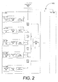
- FIG. 2 illustrates an embodiment of an I/O interface system.
- FIG. 3 illustrates an embodiment of noise graph.
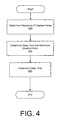
- FIG. 4 illustrates an embodiment of a noise reduction method that may be implemented by the system of FIG. 1 .
- references in the specification to "one embodiment”, “an embodiment”, “an example embodiment”, etc., indicate that the embodiment described may include a particular feature, structure, or characteristic, but every embodiment may not necessarily include the particular feature, structure, or characteristic. Moreover, such phrases are not necessarily referring to the same embodiment. Further, when a particular feature, structure, or characteristic is described in connection with an embodiment, it is submitted that it is within the knowledge of one skilled in the art to affect such feature, structure, or characteristic in connection with other embodiments whether or not explicitly described.
- lanes 200A, 200B, 200C...200N may be collectively referred to as lanes 200.
- delay circuits 210A, 210B... 210N may be collectively referred as delays 210.
- the computer system may include a processor 100, a chipset 110, a memory 120, and I/O (input/output) devices 130.
- the processor 100 may be coupled with the chipset 110 via a processor bus.
- the memory 120 may be coupled with the chipset 110 via a memory bus.
- the I/O devices 130 may be coupled with the chipset 110 via an I/O bus such as, for example, PCI (Peripheral Component Interconnect) buses, PCI Express buses, USB (Universal Serial Bus) buses, SATA (Serial Advanced Technology Attachment) buses, etc.
- PCI Peripheral Component Interconnect
- PCI Express Peripheral Component Interconnect
- USB Universal Serial Bus
- SATA Serial Advanced Technology Attachment
- the processor 100 may be implemented with an Intel ® Pentium ® 4 processor, Intel ® Pentium ® M processor, and/or another type of general purpose processor 100 capable of executing software and/or firmware instructions.
- the processor 100 may execute instructions stored in the memory 120 to perform various tasks and to control the overall operation of the computer system.
- the processor 100 may also execute instructions and/or routines related to power management such as, causing a component such as an I/O interface to reduce AC noise during operation of the system.
- the chipset 110 may comprise one or more integrated circuits or chips to couple the processors 100 with other components of the computer system.
- the chipset 110 may comprise a memory controller hub (MCH) 140 and an I/O controller hub (ICH) 150.
- the memory controller hub 140 may provide an interface to memory devices of the memory 120.
- the memory controller hub 140 may generate signals on the memory bus to read and/or write data to memory devices of the memory 120 in response to requests from the processor 100 and I/O devices 130.
- the memory 120 may comprise for example RAM (Random Access Memory) devices such as source synchronous dynamic RAM devices and DDR (Double Data Rate) RAM devices.
- the I/O controller hub 150 may comprise an I/O interface 160 such as, for example, a PCI Express interface.
- the I/O interface 160 may interface the I/O devices 130 with the I/O controller hub 150, thus permitting data transfers between the processor 100 and the I/O devices 130 and between the memory 120 and the I/O devices 130.
- the I/O interface 160 may be present in processor 100 or in memory controller hub 140.
- the computer system may also comprise I/O devices 130.
- the I/O device 130 may implement various input/output functions for the computer system.
- the I/O device 130 may comprise hard disk drives, keyboards, mice, CD (compact disc) drives, DVD (digital video discs) drives, printers, scanners, etc.
- the I/O interface system 160 may comprise a plurality of ports 270 including a plurality of lanes 200 such as for example 200A, 200B, 200C...200N, a plurality of delay circuits 210 such as for example 210A, 210B, 210C...210N, a delay control logic 220 and a power delivery network 260.
- the lane 200A may be coupled to the lane 200 B through a delay circuit 210A provided between the lanes 200 A - 200 B and lane 200 B may be coupled to the lane 200 C through another delay circuit 210 B provided between the lanes 200B and 200C and so on up to lane 200N having a delay circuit 210N between the adjoining lanes 200.
- the delay control logic 220 may be coupled to each delay circuit 210A - 210N.
- each lane of the lanes 200 may comprise a transmitter 230, a receiver 240 and a digital circuit 250.
- power delivery network 260 may sense an impact of total effective load di/dt (instantaneous sum of all the individual lane loads) of all the operational lanes 200 and generates an AC noise during operation of the I/O system.
- the delay circuits 210 may introduce a time delay between the lanes 200 to delay the switching-on of the subsequent lanes 200.
- the delay time/time constant in the delay circuits 210 may be controlled with the help of the delay control logic 220 by varying the voltage in the delay circuits 210.
- a frequency is determined, through experimentation, which contributes the most noise to I/O interface 160 when a lane 200 of a port 270 is turned on.
- a noise graph such as depicted in fig. 3 is measured from lane 200A of port 270A to determine the frequency with the greatest noise contribution.
- a delay time may be determined to minimize noise at this frequency by turning on successive lanes so that the ports are 180 degrees out of phase at this frequency.
- this frequency is referred to as a resonant frequency of power delivery network 260.
- the delay time would be half the period or 5 ns. If the I/O interface operates at 6.4 GHz, this delay time would amount to 32 unit intervals (UI).
- delay control logic 220 may add such additional delay to the intrinsic delay to achieve the calculated delay time.
- Delay circuits 210 may also delay the turning off of each lane of each port, for example as part of a power savings scheme.
- Delay control logic 220 may supply a second delay time to delay circuits 210 for turning off each successive lane that may or may not be different than the delay time for turning on each successive lane.
- individual lane loads may be spaced uniformly to reduce an overlapping and alignment of the loads in the lanes 200.
- total effective load instantaneous sum of all the individual lane loads sensed by power delivery network 260 may be reduced substantially and the reduction in the total effective load may result in smaller AC peak to peak noise in the I/O system.
- plot 300 shows the current measurements of different frequency components on a lane being turned on.
- 100 MHz is the frequency of the greatest noise.
- plot 300 is measured at lane 200A.
- FIG. 4 an embodiment of a noise reduction method implementable by the system of FIG. 1 is illustrated.
- a frequency of greatest noise is determined.
- a noise graph such as depicted in fig. 3 is obtained to visually determine which frequency contributes the greatest noise on a lane 200 while being turned on.
- a delay time is determined that minimizes the greatest noise. In one embodiment, the delay time half the period of the frequency determined in block 400.
- the delay time is implemented in I/O interface 160.
- delay control logic 220 is configured to store the appropriate delay time for use in delay control circuits 210.
Landscapes
- Engineering & Computer Science (AREA)
- Theoretical Computer Science (AREA)
- Physics & Mathematics (AREA)
- General Engineering & Computer Science (AREA)
- General Physics & Mathematics (AREA)
- Computer Hardware Design (AREA)
- Mathematical Physics (AREA)
- Logic Circuits (AREA)
- Power Sources (AREA)
- Manipulation Of Pulses (AREA)
- Semiconductor Integrated Circuits (AREA)
- Communication Control (AREA)
- Small-Scale Networks (AREA)
- Cable Transmission Systems, Equalization Of Radio And Reduction Of Echo (AREA)
Abstract
Description
- In a high speed interface such as for example a PCI-E (peripheral components interconnect - express), CSI (common system interface), FBD (fully buffered DIMM) etc, there may be an AC (alternate current) noise caused by a total effective load di/dt (change in current/change in time) that is instantaneous sum of individual lane load and may be sensed by the I/O power supply network. Each lane of an I/O interface may have a transmitter, a receiver and other digital circuits. Each individual lane may generate a lane load. The power supply network may sense an impact of the total effective load of all the operational lanes and may exhibit the AC noise.
- The invention described herein is illustrated by way of example and not by way of limitation in the accompanying figures. For simplicity and clarity of illustration, elements illustrated in the figures are not necessarily drawn to scale. For example, the dimensions of some elements may be exaggerated relative to other elements for clarity. Further, where considered appropriate, reference labels have been repeated among the figures to indicate corresponding or analogous elements.
-
FIG. 1 illustrates an embodiment of a computer system. -
FIG. 2 illustrates an embodiment of an I/O interface system. -
FIG. 3 illustrates an embodiment of noise graph. -
FIG. 4 illustrates an embodiment of a noise reduction method that may be implemented by the system ofFIG. 1 . - In the following detailed description, numerous specific details are described in order to provide a thorough understanding of the invention. However the present invention may be practiced without these specific details. In other stances, well known methods, procedures, components and circuits have not been described in detail so as not to obscure the present invention. Further, example sizes/models/values/ranges may be given, although the present invention is not limited to these specific examples.
- References in the specification to "one embodiment", "an embodiment", "an example embodiment", etc., indicate that the embodiment described may include a particular feature, structure, or characteristic, but every embodiment may not necessarily include the particular feature, structure, or characteristic. Moreover, such phrases are not necessarily referring to the same embodiment. Further, when a particular feature, structure, or characteristic is described in connection with an embodiment, it is submitted that it is within the knowledge of one skilled in the art to affect such feature, structure, or characteristic in connection with other embodiments whether or not explicitly described.
- Furthermore, elements referred to herein with a common reference label followed by a particular number may be collectively referred to by the reference label alone. For example,
lanes lanes 200. Similarlydelay circuits - Referring to
FIG. 1 , an embodiment of a computer system is shown. The computer system may include aprocessor 100, achipset 110, amemory 120, and I/O (input/output)devices 130. As depicted, theprocessor 100 may be coupled with thechipset 110 via a processor bus. Thememory 120 may be coupled with thechipset 110 via a memory bus. The I/O devices 130 may be coupled with thechipset 110 via an I/O bus such as, for example, PCI (Peripheral Component Interconnect) buses, PCI Express buses, USB (Universal Serial Bus) buses, SATA (Serial Advanced Technology Attachment) buses, etc. - The
processor 100 may be implemented with an Intel® Pentium® 4 processor, Intel® Pentium® M processor, and/or another type ofgeneral purpose processor 100 capable of executing software and/or firmware instructions. In one embodiment, theprocessor 100 may execute instructions stored in thememory 120 to perform various tasks and to control the overall operation of the computer system. Theprocessor 100 may also execute instructions and/or routines related to power management such as, causing a component such as an I/O interface to reduce AC noise during operation of the system. - The
chipset 110 may comprise one or more integrated circuits or chips to couple theprocessors 100 with other components of the computer system. As depicted, thechipset 110 may comprise a memory controller hub (MCH) 140 and an I/O controller hub (ICH) 150. Thememory controller hub 140 may provide an interface to memory devices of thememory 120. In particular, thememory controller hub 140 may generate signals on the memory bus to read and/or write data to memory devices of thememory 120 in response to requests from theprocessor 100 and I/O devices 130. Thememory 120 may comprise for example RAM (Random Access Memory) devices such as source synchronous dynamic RAM devices and DDR (Double Data Rate) RAM devices. - The I/
O controller hub 150 according to an embodiment may comprise an I/O interface 160 such as, for example, a PCI Express interface. The I/O interface 160 may interface the I/O devices 130 with the I/O controller hub 150, thus permitting data transfers between theprocessor 100 and the I/O devices 130 and between thememory 120 and the I/O devices 130. In one embodiment the I/O interface 160 may be present inprocessor 100 or inmemory controller hub 140. - As depicted, the computer system may also comprise I/
O devices 130. The I/O device 130 may implement various input/output functions for the computer system. For example, the I/O device 130 may comprise hard disk drives, keyboards, mice, CD (compact disc) drives, DVD (digital video discs) drives, printers, scanners, etc. - Referring to
FIG. 2 , an embodiment of an I/O interface system 160 is shown. As depicted the I/O interface system 160 may comprise a plurality of ports 270 including a plurality oflanes 200 such as for example 200A, 200B, 200C...200N, a plurality of delay circuits 210 such as for example 210A, 210B, 210C...210N, adelay control logic 220 and apower delivery network 260. Thelane 200A may be coupled to thelane 200 B through adelay circuit 210A provided between thelanes 200 A - 200 B andlane 200 B may be coupled to thelane 200 C through anotherdelay circuit 210 B provided between thelanes lane 200N having adelay circuit 210N between theadjoining lanes 200. Thedelay control logic 220 may be coupled to eachdelay circuit 210A - 210N. - As depicted each lane of the
lanes 200, in one embodiment, may comprise atransmitter 230, areceiver 240 and adigital circuit 250. When the power is supplied bypower delivery network 260 to the ports 270 of I/O system all thelanes 200, may be switched-on simultaneously and due totransmitter 230,receiver 240, anddigital circuit 250 in thelanes 200, eachlane 200A-200N may contribute a lane load on the power supply network.Power delivery network 260 may sense an impact of total effective load di/dt (instantaneous sum of all the individual lane loads) of all theoperational lanes 200 and generates an AC noise during operation of the I/O system. The delay circuits 210 may introduce a time delay between thelanes 200 to delay the switching-on of thesubsequent lanes 200. In one embodiment the delay time/time constant in the delay circuits 210 may be controlled with the help of thedelay control logic 220 by varying the voltage in the delay circuits 210. - In one embodiment to calculate programmed delay time, a frequency is determined, through experimentation, which contributes the most noise to I/
O interface 160 when alane 200 of a port 270 is turned on. In one example, a noise graph such as depicted infig. 3 is measured fromlane 200A ofport 270A to determine the frequency with the greatest noise contribution. Based on this frequency a delay time may be determined to minimize noise at this frequency by turning on successive lanes so that the ports are 180 degrees out of phase at this frequency. In one embodiment, this frequency is referred to as a resonant frequency ofpower delivery network 260. In the case where this frequency is 100 MHz, the delay time would be half the period or 5 ns. If the I/O interface operates at 6.4 GHz, this delay time would amount to 32 unit intervals (UI). - In one embodiment, there may be an intrinsic delay between lanes and
delay control logic 220 may add such additional delay to the intrinsic delay to achieve the calculated delay time. Delay circuits 210 may also delay the turning off of each lane of each port, for example as part of a power savings scheme.Delay control logic 220 may supply a second delay time to delay circuits 210 for turning off each successive lane that may or may not be different than the delay time for turning on each successive lane. - In one embodiment, by introducing the programmed delay circuits 210 between the
lanes 200, individual lane loads may be spaced uniformly to reduce an overlapping and alignment of the loads in thelanes 200. Thus total effective load (instantaneous sum of all the individual lane loads) sensed bypower delivery network 260 may be reduced substantially and the reduction in the total effective load may result in smaller AC peak to peak noise in the I/O system. - Referring now to
FIG. 3 , one embodiment of a noise graph is illustrated. As depicted,plot 300 shows the current measurements of different frequency components on a lane being turned on. In this example, 100 MHz is the frequency of the greatest noise. In one embodiment,plot 300 is measured atlane 200A. - Referring now to
FIG. 4 , an embodiment of a noise reduction method implementable by the system ofFIG. 1 is illustrated. As depicted inblock 400, a frequency of greatest noise is determined. In one embodiment, a noise graph, such as depicted infig. 3 is obtained to visually determine which frequency contributes the greatest noise on alane 200 while being turned on. - In
block 410, a delay time is determined that minimizes the greatest noise. In one embodiment, the delay time half the period of the frequency determined inblock 400. - In
block 420, as depicted, the delay time is implemented in I/O interface 160. In one embodiment,delay control logic 220 is configured to store the appropriate delay time for use in delay control circuits 210. - Certain features of the invention have been described with reference to example embodiments. However, the description is not intended to be construed in a limiting sense. Various modifications of the example embodiments, as well as other embodiments of the invention, which are apparent to persons skilled in the art to which the invention pertains are deemed to lie within the spirit and scope of the invention.
Claims (13)
- A method comprising:determining a frequency of a greatest noise on a high-speed data link when turning on a power delivery network;determining a delay time between a first port and a second port that minimizes the greatest noise; andturning on the second port after the delay time from turning on the first port.
- The method of claim 1, wherein determining the frequency of the greatest noise comprises determining a resonant frequency of the power delivery network.
- The method of claim 1, wherein the frequency is about 100 megahertz (MHz).
- The method of claim 1, wherein the delay time is about 32 unit intervals.
- The method of claim 1, further comprising turning on a third port after the delay time from turning on the second port.
- The method of claim 1, further comprising turning off the second port after the delay time from turning off the first port.
- An I/O interface comprising
a plurality of lanes to be switched on;
a delay circuit to provide a programmed delay between the lanes to switch-on successive lanes after the programmed delay; and
a delay control logic to control the time delay in the delay circuit, wherein the delay time is determined to minimize a greatest noise on a lane when turning on a power delivery network. - The I/O interface of claim 7, wherein the delay time is half a period of a frequency of the greatest noise.
- The I/O interface of claim 7, wherein the delay time is about 32 unit intervals.
- The I/O interface of claim 7, wherein the highest noise occurs at a resonant frequency of the power delivery network.
- The I/O interface of claim 7, further comprising the delay circuit to provide a second programmed delay between the lanes to switch-off successive lanes after the second programmed delay.
- The I/O interface of claim 11, wherein the first and second programmed delays are substantially the same.
- A system comprising
a processor;
a chipset to facilitate I/O signal to be transmitted to a computer system;
I/O devices to provide instructions to the computer system; and
I/O interfaces as claimed in any of claims 7 to 12 to couple the I/O devices with the chipset to provide a programmed delay between the lanes to switch-on successive lanes after the programmed delay, wherein the programmed delay is determined to minimize a greatest noise on a lane when turning on a power delivery network.
Applications Claiming Priority (1)
| Application Number | Priority Date | Filing Date | Title |
|---|---|---|---|
| US11/967,726 US7975158B2 (en) | 2007-12-31 | 2007-12-31 | Noise reduction method by implementing certain port-to-port delay |
Publications (3)
| Publication Number | Publication Date |
|---|---|
| EP2077482A2 true EP2077482A2 (en) | 2009-07-08 |
| EP2077482A3 EP2077482A3 (en) | 2011-05-25 |
| EP2077482B1 EP2077482B1 (en) | 2012-10-31 |
Family
ID=40600018
Family Applications (1)
| Application Number | Title | Priority Date | Filing Date |
|---|---|---|---|
| EP08254029A Ceased EP2077482B1 (en) | 2007-12-31 | 2008-12-17 | Noise reduction method by implementing certain port-to-port delay |
Country Status (6)
| Country | Link |
|---|---|
| US (1) | US7975158B2 (en) |
| EP (1) | EP2077482B1 (en) |
| JP (1) | JP4921451B2 (en) |
| CN (1) | CN101483486B (en) |
| RU (1) | RU2406106C2 (en) |
| TW (1) | TWI408540B (en) |
Families Citing this family (5)
| Publication number | Priority date | Publication date | Assignee | Title |
|---|---|---|---|---|
| JP2010188752A (en) * | 2009-02-16 | 2010-09-02 | Panasonic Corp | Noise reduction device |
| TWI408899B (en) * | 2010-04-01 | 2013-09-11 | Hon Hai Prec Ind Co Ltd | Computer motherboard and sata hard disk power supply circuit |
| US9454213B2 (en) * | 2013-12-26 | 2016-09-27 | Intel Corporation | Method, apparatus, system for lane staggering and determinism for serial high speed I/O lanes |
| CN105868131B (en) * | 2016-04-20 | 2019-10-15 | 京东方科技集团股份有限公司 | Delay control equipment, delay control method and electronic device |
| US10122209B1 (en) * | 2017-06-20 | 2018-11-06 | Intel Corporation | Tunable delay control of a power delivery network |
Citations (1)
| Publication number | Priority date | Publication date | Assignee | Title |
|---|---|---|---|---|
| US5673412A (en) | 1990-07-13 | 1997-09-30 | Hitachi, Ltd. | Disk system and power-on sequence for the same |
Family Cites Families (19)
| Publication number | Priority date | Publication date | Assignee | Title |
|---|---|---|---|---|
| US4475172A (en) * | 1978-05-30 | 1984-10-02 | Bally Manufacturing Corporation | Audio/visual home computer and game apparatus |
| US5297142A (en) * | 1991-07-18 | 1994-03-22 | Motorola, Inc. | Data transfer method and apparatus for communication between a peripheral and a master |
| KR100253076B1 (en) * | 1997-05-02 | 2000-05-01 | 윤종용 | Power-on reset circuit |
| US6009488A (en) | 1997-11-07 | 1999-12-28 | Microlinc, Llc | Computer having packet-based interconnect channel |
| TW482912B (en) * | 1998-03-02 | 2002-04-11 | Advanced Display Kk | Liquid crystal display device, integrated circuit therefor, method for driving a liquid crystal display device, and apparatus therefor |
| JP2000074983A (en) * | 1998-08-27 | 2000-03-14 | Sharp Corp | Test method for semiconductor integrated circuit |
| US6535075B2 (en) * | 1999-12-16 | 2003-03-18 | International Business Machines Corporation | Tunable on-chip capacity |
| US6566903B1 (en) * | 1999-12-28 | 2003-05-20 | Intel Corporation | Method and apparatus for dynamically controlling the performance of buffers under different performance conditions |
| US6650575B1 (en) * | 2001-12-28 | 2003-11-18 | Netlogic Microsystems, Inc. | Programmable delay circuit within a content addressable memory |
| AU2003244763A1 (en) * | 2002-05-31 | 2003-12-19 | Matsushita Electric Industrial Co., Ltd. | Bandwidth adaptation rule for adaptive noise filter for inverse filtering with improved disturbance rejection bandwidth and speed |
| JP2004233235A (en) * | 2003-01-31 | 2004-08-19 | Matsushita Electric Ind Co Ltd | Noise detection circuit and information processing device |
| JP2006018331A (en) * | 2004-06-30 | 2006-01-19 | Matsushita Electric Ind Co Ltd | Microcomputer and interrupt processing method in microcomputer |
| TWI283113B (en) * | 2005-02-24 | 2007-06-21 | Faraday Tech Corp | High-speed low-noise voltage-controlled delay cell |
| JP2007173893A (en) * | 2005-12-19 | 2007-07-05 | Hitachi Ulsi Systems Co Ltd | Semiconductor integrated circuit device |
| US7664215B2 (en) | 2005-12-21 | 2010-02-16 | Intel Corporation | Signal alignment based on data signal |
| US8166215B2 (en) | 2005-12-28 | 2012-04-24 | Intel Corporation | Method to control delay between lanes |
| JP4893064B2 (en) * | 2006-03-30 | 2012-03-07 | 富士通セミコンダクター株式会社 | Semiconductor integrated circuit and semiconductor integrated circuit design method |
| US7492605B2 (en) | 2006-06-22 | 2009-02-17 | Intel Corporation | Power plane to reduce voltage difference between connector power pins |
| US20090248945A1 (en) * | 2008-03-31 | 2009-10-01 | Navindra Navaratnam | Noise reducing methods and circuits |
-
2007
- 2007-12-31 US US11/967,726 patent/US7975158B2/en not_active Expired - Fee Related
-
2008
- 2008-12-10 TW TW097148023A patent/TWI408540B/en active
- 2008-12-17 EP EP08254029A patent/EP2077482B1/en not_active Ceased
- 2008-12-18 JP JP2008322188A patent/JP4921451B2/en not_active Expired - Fee Related
- 2008-12-26 RU RU2008151966/07A patent/RU2406106C2/en not_active IP Right Cessation
- 2008-12-31 CN CN200810190334.4A patent/CN101483486B/en not_active Expired - Fee Related
Patent Citations (1)
| Publication number | Priority date | Publication date | Assignee | Title |
|---|---|---|---|---|
| US5673412A (en) | 1990-07-13 | 1997-09-30 | Hitachi, Ltd. | Disk system and power-on sequence for the same |
Also Published As
| Publication number | Publication date |
|---|---|
| JP2009165120A (en) | 2009-07-23 |
| JP4921451B2 (en) | 2012-04-25 |
| US20090259787A1 (en) | 2009-10-15 |
| RU2406106C2 (en) | 2010-12-10 |
| RU2008151966A (en) | 2010-07-10 |
| CN101483486A (en) | 2009-07-15 |
| EP2077482B1 (en) | 2012-10-31 |
| TW200945013A (en) | 2009-11-01 |
| EP2077482A3 (en) | 2011-05-25 |
| US7975158B2 (en) | 2011-07-05 |
| TWI408540B (en) | 2013-09-11 |
| CN101483486B (en) | 2013-06-19 |
Similar Documents
| Publication | Publication Date | Title |
|---|---|---|
| US20110198942A1 (en) | Power Switch Ramp Rate Control Using Programmable Connection to Switches | |
| US20110198941A1 (en) | Power Switch Ramp Rate Control Using Daisy-Chained Flops | |
| US11144410B2 (en) | System and method to dynamically increase memory channel robustness at high transfer rates | |
| US20110185145A1 (en) | Semiconductor storage device and control method thereof | |
| EP2077482B1 (en) | Noise reduction method by implementing certain port-to-port delay | |
| KR102749976B1 (en) | System on chip controlling memory power using handshake process and operating method thereof | |
| US20080162855A1 (en) | Memory Command Issue Rate Controller | |
| US7454637B2 (en) | Voltage regulator having reduced droop | |
| US10651734B2 (en) | System and method for robust body braking control to suppress transient voltage overshoot | |
| CN105247498B (en) | The controller related method thereof and device of general Intrusion Detection based on host | |
| US5887150A (en) | SCSI controller having output driver with slew rate control | |
| US20190065295A1 (en) | Storage Server System Capable of Setting Overcurrent Protection Value According to System Configuration | |
| CN102867158B (en) | A kind of switch internal memory method, device and there is the terminal of dual system | |
| US11222687B2 (en) | System and method for power plane noise reduction in a memory subsystem of an information handling system | |
| US8304698B1 (en) | Thermal throttling of peripheral components in a processing device | |
| KR20240033030A (en) | In-band communication interface power management fencing | |
| US20210048863A1 (en) | System and Method for Controlling a Power-On Sequence and Power Throttling using Power Brake | |
| US10877918B2 (en) | System and method for I/O aware processor configuration | |
| TWI703576B (en) | Memory access control | |
| US6842831B2 (en) | Low latency buffer control system and method | |
| US8166215B2 (en) | Method to control delay between lanes | |
| KR100687925B1 (en) | Computer systems | |
| US8417985B2 (en) | Adjusting system clock to faster speed upon receiving mass storage command and back to lower speed upon completion of all commands | |
| US20180004274A1 (en) | Determining power state support | |
| CN1809824A (en) | Active termination control via registers on the module |
Legal Events
| Date | Code | Title | Description |
|---|---|---|---|
| PUAI | Public reference made under article 153(3) epc to a published international application that has entered the european phase |
Free format text: ORIGINAL CODE: 0009012 |
|
| AK | Designated contracting states |
Kind code of ref document: A2 Designated state(s): AT BE BG CH CY CZ DE DK EE ES FI FR GB GR HR HU IE IS IT LI LT LU LV MC MT NL NO PL PT RO SE SI SK TR |
|
| AX | Request for extension of the european patent |
Extension state: AL BA MK RS |
|
| PUAL | Search report despatched |
Free format text: ORIGINAL CODE: 0009013 |
|
| AK | Designated contracting states |
Kind code of ref document: A3 Designated state(s): AT BE BG CH CY CZ DE DK EE ES FI FR GB GR HR HU IE IS IT LI LT LU LV MC MT NL NO PL PT RO SE SI SK TR |
|
| AX | Request for extension of the european patent |
Extension state: AL BA MK RS |
|
| RIC1 | Information provided on ipc code assigned before grant |
Ipc: G06F 13/00 20060101ALI20110420BHEP Ipc: G06F 1/18 20060101ALI20110420BHEP Ipc: G06F 1/32 20060101ALI20110420BHEP Ipc: G06F 1/26 20060101AFI20090512BHEP |
|
| 17P | Request for examination filed |
Effective date: 20111116 |
|
| AKX | Designation fees paid |
Designated state(s): DE GB |
|
| RIC1 | Information provided on ipc code assigned before grant |
Ipc: G06F 13/00 20060101ALI20120320BHEP Ipc: G06F 1/18 20060101ALI20120320BHEP Ipc: G06F 1/32 20060101ALI20120320BHEP Ipc: G06F 13/40 20060101ALI20120320BHEP Ipc: G06F 1/26 20060101AFI20120320BHEP |
|
| GRAP | Despatch of communication of intention to grant a patent |
Free format text: ORIGINAL CODE: EPIDOSNIGR1 |
|
| GRAS | Grant fee paid |
Free format text: ORIGINAL CODE: EPIDOSNIGR3 |
|
| GRAA | (expected) grant |
Free format text: ORIGINAL CODE: 0009210 |
|
| AK | Designated contracting states |
Kind code of ref document: B1 Designated state(s): DE GB |
|
| REG | Reference to a national code |
Ref country code: GB Ref legal event code: FG4D |
|
| REG | Reference to a national code |
Ref country code: DE Ref legal event code: R096 Ref document number: 602008019751 Country of ref document: DE Effective date: 20121227 |
|
| PLBE | No opposition filed within time limit |
Free format text: ORIGINAL CODE: 0009261 |
|
| STAA | Information on the status of an ep patent application or granted ep patent |
Free format text: STATUS: NO OPPOSITION FILED WITHIN TIME LIMIT |
|
| 26N | No opposition filed |
Effective date: 20130801 |
|
| REG | Reference to a national code |
Ref country code: DE Ref legal event code: R097 Ref document number: 602008019751 Country of ref document: DE Effective date: 20130801 |
|
| PGFP | Annual fee paid to national office [announced via postgrant information from national office to epo] |
Ref country code: GB Payment date: 20211118 Year of fee payment: 14 Ref country code: DE Payment date: 20211116 Year of fee payment: 14 |
|
| P01 | Opt-out of the competence of the unified patent court (upc) registered |
Effective date: 20230518 |
|
| REG | Reference to a national code |
Ref country code: DE Ref legal event code: R119 Ref document number: 602008019751 Country of ref document: DE |
|
| GBPC | Gb: european patent ceased through non-payment of renewal fee |
Effective date: 20221217 |
|
| PG25 | Lapsed in a contracting state [announced via postgrant information from national office to epo] |
Ref country code: GB Free format text: LAPSE BECAUSE OF NON-PAYMENT OF DUE FEES Effective date: 20221217 Ref country code: DE Free format text: LAPSE BECAUSE OF NON-PAYMENT OF DUE FEES Effective date: 20230701 |