EP2076922B1 - Semiconductor device having low dielectric insulating film and manufacturing method of the same - Google Patents
Semiconductor device having low dielectric insulating film and manufacturing method of the same Download PDFInfo
- Publication number
- EP2076922B1 EP2076922B1 EP08765221A EP08765221A EP2076922B1 EP 2076922 B1 EP2076922 B1 EP 2076922B1 EP 08765221 A EP08765221 A EP 08765221A EP 08765221 A EP08765221 A EP 08765221A EP 2076922 B1 EP2076922 B1 EP 2076922B1
- Authority
- EP
- European Patent Office
- Prior art keywords
- low dielectric
- film
- wiring line
- laminated structure
- structure portion
- Prior art date
- Legal status (The legal status is an assumption and is not a legal conclusion. Google has not performed a legal analysis and makes no representation as to the accuracy of the status listed.)
- Expired - Fee Related
Links
Images


Classifications
-
- H—ELECTRICITY
- H01—ELECTRIC ELEMENTS
- H01L—SEMICONDUCTOR DEVICES NOT COVERED BY CLASS H10
- H01L23/00—Details of semiconductor or other solid state devices
- H01L23/48—Arrangements for conducting electric current to or from the solid state body in operation, e.g. leads, terminal arrangements ; Selection of materials therefor
- H01L23/482—Arrangements for conducting electric current to or from the solid state body in operation, e.g. leads, terminal arrangements ; Selection of materials therefor consisting of lead-in layers inseparably applied to the semiconductor body
- H01L23/485—Arrangements for conducting electric current to or from the solid state body in operation, e.g. leads, terminal arrangements ; Selection of materials therefor consisting of lead-in layers inseparably applied to the semiconductor body consisting of layered constructions comprising conductive layers and insulating layers, e.g. planar contacts
-
- H—ELECTRICITY
- H01—ELECTRIC ELEMENTS
- H01L—SEMICONDUCTOR DEVICES NOT COVERED BY CLASS H10
- H01L23/00—Details of semiconductor or other solid state devices
- H01L23/28—Encapsulations, e.g. encapsulating layers, coatings, e.g. for protection
- H01L23/31—Encapsulations, e.g. encapsulating layers, coatings, e.g. for protection characterised by the arrangement or shape
- H01L23/3107—Encapsulations, e.g. encapsulating layers, coatings, e.g. for protection characterised by the arrangement or shape the device being completely enclosed
- H01L23/3114—Encapsulations, e.g. encapsulating layers, coatings, e.g. for protection characterised by the arrangement or shape the device being completely enclosed the device being a chip scale package, e.g. CSP
-
- H—ELECTRICITY
- H01—ELECTRIC ELEMENTS
- H01L—SEMICONDUCTOR DEVICES NOT COVERED BY CLASS H10
- H01L23/00—Details of semiconductor or other solid state devices
- H01L23/52—Arrangements for conducting electric current within the device in operation from one component to another, i.e. interconnections, e.g. wires, lead frames
- H01L23/522—Arrangements for conducting electric current within the device in operation from one component to another, i.e. interconnections, e.g. wires, lead frames including external interconnections consisting of a multilayer structure of conductive and insulating layers inseparably formed on the semiconductor body
- H01L23/525—Arrangements for conducting electric current within the device in operation from one component to another, i.e. interconnections, e.g. wires, lead frames including external interconnections consisting of a multilayer structure of conductive and insulating layers inseparably formed on the semiconductor body with adaptable interconnections
-
- H—ELECTRICITY
- H01—ELECTRIC ELEMENTS
- H01L—SEMICONDUCTOR DEVICES NOT COVERED BY CLASS H10
- H01L24/00—Arrangements for connecting or disconnecting semiconductor or solid-state bodies; Methods or apparatus related thereto
- H01L24/01—Means for bonding being attached to, or being formed on, the surface to be connected, e.g. chip-to-package, die-attach, "first-level" interconnects; Manufacturing methods related thereto
- H01L24/10—Bump connectors ; Manufacturing methods related thereto
- H01L24/11—Manufacturing methods
-
- H—ELECTRICITY
- H01—ELECTRIC ELEMENTS
- H01L—SEMICONDUCTOR DEVICES NOT COVERED BY CLASS H10
- H01L24/00—Arrangements for connecting or disconnecting semiconductor or solid-state bodies; Methods or apparatus related thereto
- H01L24/93—Batch processes
- H01L24/94—Batch processes at wafer-level, i.e. with connecting carried out on a wafer comprising a plurality of undiced individual devices
-
- H—ELECTRICITY
- H01—ELECTRIC ELEMENTS
- H01L—SEMICONDUCTOR DEVICES NOT COVERED BY CLASS H10
- H01L2224/00—Indexing scheme for arrangements for connecting or disconnecting semiconductor or solid-state bodies and methods related thereto as covered by H01L24/00
- H01L2224/01—Means for bonding being attached to, or being formed on, the surface to be connected, e.g. chip-to-package, die-attach, "first-level" interconnects; Manufacturing methods related thereto
- H01L2224/02—Bonding areas; Manufacturing methods related thereto
- H01L2224/023—Redistribution layers [RDL] for bonding areas
- H01L2224/0231—Manufacturing methods of the redistribution layers
-
- H—ELECTRICITY
- H01—ELECTRIC ELEMENTS
- H01L—SEMICONDUCTOR DEVICES NOT COVERED BY CLASS H10
- H01L2224/00—Indexing scheme for arrangements for connecting or disconnecting semiconductor or solid-state bodies and methods related thereto as covered by H01L24/00
- H01L2224/01—Means for bonding being attached to, or being formed on, the surface to be connected, e.g. chip-to-package, die-attach, "first-level" interconnects; Manufacturing methods related thereto
- H01L2224/02—Bonding areas; Manufacturing methods related thereto
- H01L2224/023—Redistribution layers [RDL] for bonding areas
- H01L2224/0233—Structure of the redistribution layers
- H01L2224/02331—Multilayer structure
-
- H—ELECTRICITY
- H01—ELECTRIC ELEMENTS
- H01L—SEMICONDUCTOR DEVICES NOT COVERED BY CLASS H10
- H01L2224/00—Indexing scheme for arrangements for connecting or disconnecting semiconductor or solid-state bodies and methods related thereto as covered by H01L24/00
- H01L2224/01—Means for bonding being attached to, or being formed on, the surface to be connected, e.g. chip-to-package, die-attach, "first-level" interconnects; Manufacturing methods related thereto
- H01L2224/02—Bonding areas; Manufacturing methods related thereto
- H01L2224/023—Redistribution layers [RDL] for bonding areas
- H01L2224/0237—Disposition of the redistribution layers
- H01L2224/02377—Fan-in arrangement
-
- H—ELECTRICITY
- H01—ELECTRIC ELEMENTS
- H01L—SEMICONDUCTOR DEVICES NOT COVERED BY CLASS H10
- H01L2224/00—Indexing scheme for arrangements for connecting or disconnecting semiconductor or solid-state bodies and methods related thereto as covered by H01L24/00
- H01L2224/01—Means for bonding being attached to, or being formed on, the surface to be connected, e.g. chip-to-package, die-attach, "first-level" interconnects; Manufacturing methods related thereto
- H01L2224/02—Bonding areas; Manufacturing methods related thereto
- H01L2224/04—Structure, shape, material or disposition of the bonding areas prior to the connecting process
- H01L2224/0401—Bonding areas specifically adapted for bump connectors, e.g. under bump metallisation [UBM]
-
- H—ELECTRICITY
- H01—ELECTRIC ELEMENTS
- H01L—SEMICONDUCTOR DEVICES NOT COVERED BY CLASS H10
- H01L2224/00—Indexing scheme for arrangements for connecting or disconnecting semiconductor or solid-state bodies and methods related thereto as covered by H01L24/00
- H01L2224/01—Means for bonding being attached to, or being formed on, the surface to be connected, e.g. chip-to-package, die-attach, "first-level" interconnects; Manufacturing methods related thereto
- H01L2224/02—Bonding areas; Manufacturing methods related thereto
- H01L2224/04—Structure, shape, material or disposition of the bonding areas prior to the connecting process
- H01L2224/04105—Bonding areas formed on an encapsulation of the semiconductor or solid-state body, e.g. bonding areas on chip-scale packages
-
- H—ELECTRICITY
- H01—ELECTRIC ELEMENTS
- H01L—SEMICONDUCTOR DEVICES NOT COVERED BY CLASS H10
- H01L2224/00—Indexing scheme for arrangements for connecting or disconnecting semiconductor or solid-state bodies and methods related thereto as covered by H01L24/00
- H01L2224/01—Means for bonding being attached to, or being formed on, the surface to be connected, e.g. chip-to-package, die-attach, "first-level" interconnects; Manufacturing methods related thereto
- H01L2224/02—Bonding areas; Manufacturing methods related thereto
- H01L2224/04—Structure, shape, material or disposition of the bonding areas prior to the connecting process
- H01L2224/05—Structure, shape, material or disposition of the bonding areas prior to the connecting process of an individual bonding area
- H01L2224/0554—External layer
- H01L2224/0556—Disposition
- H01L2224/05569—Disposition the external layer being disposed on a redistribution layer on the semiconductor or solid-state body
-
- H—ELECTRICITY
- H01—ELECTRIC ELEMENTS
- H01L—SEMICONDUCTOR DEVICES NOT COVERED BY CLASS H10
- H01L2224/00—Indexing scheme for arrangements for connecting or disconnecting semiconductor or solid-state bodies and methods related thereto as covered by H01L24/00
- H01L2224/01—Means for bonding being attached to, or being formed on, the surface to be connected, e.g. chip-to-package, die-attach, "first-level" interconnects; Manufacturing methods related thereto
- H01L2224/10—Bump connectors; Manufacturing methods related thereto
- H01L2224/11—Manufacturing methods
- H01L2224/1147—Manufacturing methods using a lift-off mask
-
- H—ELECTRICITY
- H01—ELECTRIC ELEMENTS
- H01L—SEMICONDUCTOR DEVICES NOT COVERED BY CLASS H10
- H01L2224/00—Indexing scheme for arrangements for connecting or disconnecting semiconductor or solid-state bodies and methods related thereto as covered by H01L24/00
- H01L2224/01—Means for bonding being attached to, or being formed on, the surface to be connected, e.g. chip-to-package, die-attach, "first-level" interconnects; Manufacturing methods related thereto
- H01L2224/10—Bump connectors; Manufacturing methods related thereto
- H01L2224/12—Structure, shape, material or disposition of the bump connectors prior to the connecting process
- H01L2224/12105—Bump connectors formed on an encapsulation of the semiconductor or solid-state body, e.g. bumps on chip-scale packages
-
- H—ELECTRICITY
- H01—ELECTRIC ELEMENTS
- H01L—SEMICONDUCTOR DEVICES NOT COVERED BY CLASS H10
- H01L2224/00—Indexing scheme for arrangements for connecting or disconnecting semiconductor or solid-state bodies and methods related thereto as covered by H01L24/00
- H01L2224/01—Means for bonding being attached to, or being formed on, the surface to be connected, e.g. chip-to-package, die-attach, "first-level" interconnects; Manufacturing methods related thereto
- H01L2224/10—Bump connectors; Manufacturing methods related thereto
- H01L2224/12—Structure, shape, material or disposition of the bump connectors prior to the connecting process
- H01L2224/13—Structure, shape, material or disposition of the bump connectors prior to the connecting process of an individual bump connector
- H01L2224/13001—Core members of the bump connector
- H01L2224/1302—Disposition
- H01L2224/13022—Disposition the bump connector being at least partially embedded in the surface
-
- H—ELECTRICITY
- H01—ELECTRIC ELEMENTS
- H01L—SEMICONDUCTOR DEVICES NOT COVERED BY CLASS H10
- H01L2224/00—Indexing scheme for arrangements for connecting or disconnecting semiconductor or solid-state bodies and methods related thereto as covered by H01L24/00
- H01L2224/01—Means for bonding being attached to, or being formed on, the surface to be connected, e.g. chip-to-package, die-attach, "first-level" interconnects; Manufacturing methods related thereto
- H01L2224/10—Bump connectors; Manufacturing methods related thereto
- H01L2224/12—Structure, shape, material or disposition of the bump connectors prior to the connecting process
- H01L2224/13—Structure, shape, material or disposition of the bump connectors prior to the connecting process of an individual bump connector
- H01L2224/13001—Core members of the bump connector
- H01L2224/1302—Disposition
- H01L2224/13024—Disposition the bump connector being disposed on a redistribution layer on the semiconductor or solid-state body
-
- H—ELECTRICITY
- H01—ELECTRIC ELEMENTS
- H01L—SEMICONDUCTOR DEVICES NOT COVERED BY CLASS H10
- H01L2224/00—Indexing scheme for arrangements for connecting or disconnecting semiconductor or solid-state bodies and methods related thereto as covered by H01L24/00
- H01L2224/01—Means for bonding being attached to, or being formed on, the surface to be connected, e.g. chip-to-package, die-attach, "first-level" interconnects; Manufacturing methods related thereto
- H01L2224/10—Bump connectors; Manufacturing methods related thereto
- H01L2224/12—Structure, shape, material or disposition of the bump connectors prior to the connecting process
- H01L2224/13—Structure, shape, material or disposition of the bump connectors prior to the connecting process of an individual bump connector
- H01L2224/13001—Core members of the bump connector
- H01L2224/13099—Material
- H01L2224/131—Material with a principal constituent of the material being a metal or a metalloid, e.g. boron [B], silicon [Si], germanium [Ge], arsenic [As], antimony [Sb], tellurium [Te] and polonium [Po], and alloys thereof
-
- H—ELECTRICITY
- H01—ELECTRIC ELEMENTS
- H01L—SEMICONDUCTOR DEVICES NOT COVERED BY CLASS H10
- H01L2224/00—Indexing scheme for arrangements for connecting or disconnecting semiconductor or solid-state bodies and methods related thereto as covered by H01L24/00
- H01L2224/01—Means for bonding being attached to, or being formed on, the surface to be connected, e.g. chip-to-package, die-attach, "first-level" interconnects; Manufacturing methods related thereto
- H01L2224/26—Layer connectors, e.g. plate connectors, solder or adhesive layers; Manufacturing methods related thereto
- H01L2224/27—Manufacturing methods
- H01L2224/274—Manufacturing methods by blanket deposition of the material of the layer connector
-
- H—ELECTRICITY
- H01—ELECTRIC ELEMENTS
- H01L—SEMICONDUCTOR DEVICES NOT COVERED BY CLASS H10
- H01L23/00—Details of semiconductor or other solid state devices
- H01L23/52—Arrangements for conducting electric current within the device in operation from one component to another, i.e. interconnections, e.g. wires, lead frames
- H01L23/522—Arrangements for conducting electric current within the device in operation from one component to another, i.e. interconnections, e.g. wires, lead frames including external interconnections consisting of a multilayer structure of conductive and insulating layers inseparably formed on the semiconductor body
- H01L23/532—Arrangements for conducting electric current within the device in operation from one component to another, i.e. interconnections, e.g. wires, lead frames including external interconnections consisting of a multilayer structure of conductive and insulating layers inseparably formed on the semiconductor body characterised by the materials
- H01L23/5329—Insulating materials
- H01L23/53295—Stacked insulating layers
-
- H—ELECTRICITY
- H01—ELECTRIC ELEMENTS
- H01L—SEMICONDUCTOR DEVICES NOT COVERED BY CLASS H10
- H01L24/00—Arrangements for connecting or disconnecting semiconductor or solid-state bodies; Methods or apparatus related thereto
- H01L24/01—Means for bonding being attached to, or being formed on, the surface to be connected, e.g. chip-to-package, die-attach, "first-level" interconnects; Manufacturing methods related thereto
- H01L24/02—Bonding areas ; Manufacturing methods related thereto
- H01L24/04—Structure, shape, material or disposition of the bonding areas prior to the connecting process
- H01L24/05—Structure, shape, material or disposition of the bonding areas prior to the connecting process of an individual bonding area
-
- H—ELECTRICITY
- H01—ELECTRIC ELEMENTS
- H01L—SEMICONDUCTOR DEVICES NOT COVERED BY CLASS H10
- H01L24/00—Arrangements for connecting or disconnecting semiconductor or solid-state bodies; Methods or apparatus related thereto
- H01L24/01—Means for bonding being attached to, or being formed on, the surface to be connected, e.g. chip-to-package, die-attach, "first-level" interconnects; Manufacturing methods related thereto
- H01L24/10—Bump connectors ; Manufacturing methods related thereto
- H01L24/12—Structure, shape, material or disposition of the bump connectors prior to the connecting process
- H01L24/13—Structure, shape, material or disposition of the bump connectors prior to the connecting process of an individual bump connector
-
- H—ELECTRICITY
- H01—ELECTRIC ELEMENTS
- H01L—SEMICONDUCTOR DEVICES NOT COVERED BY CLASS H10
- H01L2924/00—Indexing scheme for arrangements or methods for connecting or disconnecting semiconductor or solid-state bodies as covered by H01L24/00
- H01L2924/0001—Technical content checked by a classifier
- H01L2924/00013—Fully indexed content
-
- H—ELECTRICITY
- H01—ELECTRIC ELEMENTS
- H01L—SEMICONDUCTOR DEVICES NOT COVERED BY CLASS H10
- H01L2924/00—Indexing scheme for arrangements or methods for connecting or disconnecting semiconductor or solid-state bodies as covered by H01L24/00
- H01L2924/01—Chemical elements
- H01L2924/01005—Boron [B]
-
- H—ELECTRICITY
- H01—ELECTRIC ELEMENTS
- H01L—SEMICONDUCTOR DEVICES NOT COVERED BY CLASS H10
- H01L2924/00—Indexing scheme for arrangements or methods for connecting or disconnecting semiconductor or solid-state bodies as covered by H01L24/00
- H01L2924/01—Chemical elements
- H01L2924/01006—Carbon [C]
-
- H—ELECTRICITY
- H01—ELECTRIC ELEMENTS
- H01L—SEMICONDUCTOR DEVICES NOT COVERED BY CLASS H10
- H01L2924/00—Indexing scheme for arrangements or methods for connecting or disconnecting semiconductor or solid-state bodies as covered by H01L24/00
- H01L2924/01—Chemical elements
- H01L2924/01013—Aluminum [Al]
-
- H—ELECTRICITY
- H01—ELECTRIC ELEMENTS
- H01L—SEMICONDUCTOR DEVICES NOT COVERED BY CLASS H10
- H01L2924/00—Indexing scheme for arrangements or methods for connecting or disconnecting semiconductor or solid-state bodies as covered by H01L24/00
- H01L2924/01—Chemical elements
- H01L2924/01015—Phosphorus [P]
-
- H—ELECTRICITY
- H01—ELECTRIC ELEMENTS
- H01L—SEMICONDUCTOR DEVICES NOT COVERED BY CLASS H10
- H01L2924/00—Indexing scheme for arrangements or methods for connecting or disconnecting semiconductor or solid-state bodies as covered by H01L24/00
- H01L2924/01—Chemical elements
- H01L2924/01019—Potassium [K]
-
- H—ELECTRICITY
- H01—ELECTRIC ELEMENTS
- H01L—SEMICONDUCTOR DEVICES NOT COVERED BY CLASS H10
- H01L2924/00—Indexing scheme for arrangements or methods for connecting or disconnecting semiconductor or solid-state bodies as covered by H01L24/00
- H01L2924/01—Chemical elements
- H01L2924/01022—Titanium [Ti]
-
- H—ELECTRICITY
- H01—ELECTRIC ELEMENTS
- H01L—SEMICONDUCTOR DEVICES NOT COVERED BY CLASS H10
- H01L2924/00—Indexing scheme for arrangements or methods for connecting or disconnecting semiconductor or solid-state bodies as covered by H01L24/00
- H01L2924/01—Chemical elements
- H01L2924/01029—Copper [Cu]
-
- H—ELECTRICITY
- H01—ELECTRIC ELEMENTS
- H01L—SEMICONDUCTOR DEVICES NOT COVERED BY CLASS H10
- H01L2924/00—Indexing scheme for arrangements or methods for connecting or disconnecting semiconductor or solid-state bodies as covered by H01L24/00
- H01L2924/01—Chemical elements
- H01L2924/01033—Arsenic [As]
-
- H—ELECTRICITY
- H01—ELECTRIC ELEMENTS
- H01L—SEMICONDUCTOR DEVICES NOT COVERED BY CLASS H10
- H01L2924/00—Indexing scheme for arrangements or methods for connecting or disconnecting semiconductor or solid-state bodies as covered by H01L24/00
- H01L2924/01—Chemical elements
- H01L2924/01047—Silver [Ag]
-
- H—ELECTRICITY
- H01—ELECTRIC ELEMENTS
- H01L—SEMICONDUCTOR DEVICES NOT COVERED BY CLASS H10
- H01L2924/00—Indexing scheme for arrangements or methods for connecting or disconnecting semiconductor or solid-state bodies as covered by H01L24/00
- H01L2924/01—Chemical elements
- H01L2924/01078—Platinum [Pt]
-
- H—ELECTRICITY
- H01—ELECTRIC ELEMENTS
- H01L—SEMICONDUCTOR DEVICES NOT COVERED BY CLASS H10
- H01L2924/00—Indexing scheme for arrangements or methods for connecting or disconnecting semiconductor or solid-state bodies as covered by H01L24/00
- H01L2924/013—Alloys
- H01L2924/014—Solder alloys
-
- H—ELECTRICITY
- H01—ELECTRIC ELEMENTS
- H01L—SEMICONDUCTOR DEVICES NOT COVERED BY CLASS H10
- H01L2924/00—Indexing scheme for arrangements or methods for connecting or disconnecting semiconductor or solid-state bodies as covered by H01L24/00
- H01L2924/10—Details of semiconductor or other solid state devices to be connected
- H01L2924/11—Device type
- H01L2924/12—Passive devices, e.g. 2 terminal devices
- H01L2924/1204—Optical Diode
- H01L2924/12042—LASER
-
- H—ELECTRICITY
- H01—ELECTRIC ELEMENTS
- H01L—SEMICONDUCTOR DEVICES NOT COVERED BY CLASS H10
- H01L2924/00—Indexing scheme for arrangements or methods for connecting or disconnecting semiconductor or solid-state bodies as covered by H01L24/00
- H01L2924/10—Details of semiconductor or other solid state devices to be connected
- H01L2924/11—Device type
- H01L2924/12—Passive devices, e.g. 2 terminal devices
- H01L2924/1204—Optical Diode
- H01L2924/12044—OLED
-
- H—ELECTRICITY
- H01—ELECTRIC ELEMENTS
- H01L—SEMICONDUCTOR DEVICES NOT COVERED BY CLASS H10
- H01L2924/00—Indexing scheme for arrangements or methods for connecting or disconnecting semiconductor or solid-state bodies as covered by H01L24/00
- H01L2924/10—Details of semiconductor or other solid state devices to be connected
- H01L2924/11—Device type
- H01L2924/14—Integrated circuits
-
- H—ELECTRICITY
- H01—ELECTRIC ELEMENTS
- H01L—SEMICONDUCTOR DEVICES NOT COVERED BY CLASS H10
- H01L2924/00—Indexing scheme for arrangements or methods for connecting or disconnecting semiconductor or solid-state bodies as covered by H01L24/00
- H01L2924/19—Details of hybrid assemblies other than the semiconductor or other solid state devices to be connected
- H01L2924/1901—Structure
- H01L2924/1904—Component type
- H01L2924/19041—Component type being a capacitor
-
- H—ELECTRICITY
- H01—ELECTRIC ELEMENTS
- H01L—SEMICONDUCTOR DEVICES NOT COVERED BY CLASS H10
- H01L2924/00—Indexing scheme for arrangements or methods for connecting or disconnecting semiconductor or solid-state bodies as covered by H01L24/00
- H01L2924/30—Technical effects
- H01L2924/301—Electrical effects
- H01L2924/30105—Capacitance
Definitions
- the present invention relates to a semiconductor device and a method for manufacturing the same, and particularly a semiconductor device having wiring lines on a low dielectric film.
- CSPs chip size packages
- WLP wafer level package
- wiring lines are extended from connection pads on the upper surface of an insulating film which covers the connection pads formed on the semiconductor substrate, a number of columnar electrodes are respectively arranged on the upper surfaces of connection pad portions formed on ends of the extended wiring lines, and a sealing film is formed so as to cover the wiring lines between the columnar electrodes on the upper surface of the insulating film.
- the sealing film is formed so that the upper surface of the sealing film and the upper surfaces of the columnar electrodes are on one plane. Solder balls are respectively provided on the upper surfaces of the columnar electrodes.
- an interlayer insulating film wiring line laminated structure portions each including a laminated structure of interlayer insulating films and the wiring lines is provided between the semiconductor substrate and the insulating film.
- a capacity between the wiring lines increases, with the result that a delay of a signal which transmits through the wiring lines increases.
- a low dielectric material such as a low-k material having a dielectric constant lower than a dielectric constant of 4.2 to 4.0 of silicon oxide which is generally used as the material of the interlayer insulating film.
- the low-k material include SiOC obtained by doping silicon oxide (SiO 2 ) with carbon (C), and SiOCH further containing H.
- SiOC silicon oxide
- C carbon
- SiOCH SiOCH
- the low dielectric film represented by the porous type low dielectric film having a hollow structure has a small mechanical strength and is easily influenced by moisture. As a result, there is a problem that the low dielectric film easily peels from an underlayer.
- EP-A-1 298 725 relates to a semiconductor device of a multi-wiring structure, particularly, to the structure of an insulating film within the same wiring layer.
- US 2002/024145 A1 discloses a semiconductor device using a fluorinated silicate glass film as an interlayer metal dielectric film.
- EP-A-1 737 037 relates to a method for fabricating a circuitry component.
- the method comprises the steps of providing a semiconductor wafer, a first metal layer, and a first polymer layer.
- US-B1-6 559 548 relates to a wiring structure of a semiconductor device comprising a first insulating layer, a wiring layer, a second insulating layer, a first via plug, an electrode pad and a second via plug.
- US 2005/170641 A1 discloses a method for forming a buried wiring in a low-k dielectric film.
- US 2002/100984 A1 relates to a semiconductor device having wirings formed in wiring grooves and a connection member formed integrally with the wirings in via holes for connecting the wirings and lower layer wirings thereof.
- An object of the present invention is to provide a semiconductor device capable of significantly avoiding a problem of peeling of a low dielectric film, and a method for manufacturing the same.
- a semiconductor device comprises a semiconductor substrate and a low dielectric film wiring line laminated structure portion which is provided on one surface of the semiconductor substrate.
- the low dielectric film wiring line laminated structure portion has a laminated structure including a plurality of low dielectric films and a plurality of wiring lines, each of the low dielectric films having a relative dielectric constant of 3.0 or lower and a glass transition temperature of 400°C or higher.
- An insulating film is formed at least on the low dielectric film wiring line laminated structure portion.
- connection pad portion for an electrode so as to be connected to a connection pad portion of an uppermost wiring line of the low dielectric film wiring line laminated structure portion, a bump electrode for external connection, provided on the connection pad portion for the electrode, and a sealing film made of an organic resin and provided at least on a part of the insulating film which surrounds the pump electrode for the external connection.
- Side surfaces of the low dielectric film wiring line laminated structure portion are covered with one of the insulating film and the sealing film.
- a method for manufacturing a semiconductor device comprises preparing a semiconductor wafer, on one surface of which a low dielectric film wiring line laminated structure portion is formed, the low dielectric film wiring line laminated structure portion including low dielectric films and wiring lines, the low dielectric films having a relative dielectric constant of 3.0 or lower and a glass transition temperature of 400°C or higher.
- parts of the low dielectric film wiring line laminated structure portion in regions above dicing streets and regions on opposite sides of the dicing streets are removed by applying laser beams, thereby forming a groove exposing side surfaces of the low dielectric film wiring line laminated structure portion.
- an organic resin film covering the side surfaces of the low dielectric film wiring line laminated structure portion is formed.
- the organic resin film and the semiconductor wafer are cut along the dicing streets, thereby obtaining a plurality of semiconductor devices.
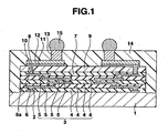
- FIG. 1 shows a sectional view of a semiconductor device as a first example.
- This semiconductor device includes a silicon substrate (a semiconductor substrate) 1.
- a number of active semiconductor elements such as transistors, are provided (not shown).
- connection pads 2 made of an aluminum-based metal or the like are electrically connected to the respective semiconductor elements, although the figure shows only two pads.
- the connection pads 2 are input and/or output terminals of each semiconductor element, and/or a power supply terminal.
- the laminated structure portion 3 has a structure in which there are alternately laminated a plurality of layers, for example, four layers of low dielectric films 4 and the same number of layers of wiring lines 5 made of copper or an aluminum-based metal or the like.
- Examples of a material of the low dielectric films 4 include a polysiloxane-based material having an Si-O bond and an Si-H bond (HSQ:Hydrogen silsesquioxane having a relative dielectric constant of 3.0), a polysiloxane-based material having an Si-O bond and an Si-CH 3 bond (MSQ:Methyl silsesquioxane having a relative dielectric constant of 2.7-2.9), carbon-doped silicon oxide (SiOC having a relative dielectric constant of 2.7-2.9) and an organic polymer-based low-k material.
- the materials having a relative dielectric constant of 3.0 or lower and a glass transition temperature of 400°C or higher can be used.
- organic polymer-based low-k material examples include "SiLK (having a relative dielectric constant of 2.6)” produced by Dow Chemical Company and “FLARE (having a relative dielectric constant of 2.8)” produced by Honeywell Electronic Materials Company.
- the glass transition temperature of 400°C or higher is a condition for tolerance to a temperature in a manufacturing step or steps to be described later.
- a porous type of each of the above materials may also be used.
- the material of the low dielectric films 4 may also be a material which has a relative dielectric constant higher than 3.0 in a normal condition, but can have a relative dielectric constant of 3.0 or lower and a glass transition temperature of 400°C or higher when it becomes porous.
- fluorinated silicate glass FSG having a relative dielectric constant of 3.5-3.7
- BSG having a relative dielectric constant of 3.5 boron-doped silicate glass
- silicon oxide having a relative dielectric constant of 4.0-4.2
- connection pad portions 5a of the wiring lines 5 of an uppermost layer are arranged on an upper surface peripheral portion of the low dielectric film 4 of the uppermost layer.
- a passivation film 7 made of an inorganic material such as silicon oxide is provided on the upper surfaces of the uppermost wiring lines 5 and the low dielectric films 4 of the uppermost layer. Openings 8 are formed through the passivation film 7 in portions corresponding to the connection pad portions 5a of the wiring lines 5 of the uppermost layer.
- a protective film (insulating film) 9 made of an organic material containing polyimide, epoxy, phenol, bismaleimide, acryl, synthetic rubber, polybenzoxide or the like as a main component. Openings 10 are formed through the protective film 9 in portions corresponding to the openings 8 of the passivation film 7.
- connection pad portions (connecting pad portions for electrodes) of the upper layer wiring lines 12 there are provided columnar electrodes (bump electrodes for external connection) 13 made of copper.
- a sealing film 14 made of an organic material such as an epoxy-based resin so that the upper surface of the sealing film and the upper surfaces of the columnar electrodes 13 are on one plane.
- the side surfaces of the low dielectric film wiring line laminated structure portion 3, the passivation film 7 and the protective film 9 form substantially one plane and are entirely covered with the sealing film 14.
- Solder balls 15 are provided on the upper surfaces of the columnar electrodes 13.
- the low dielectric film wiring line laminated structure portion or structure portions 3 each including the laminated structure of the low dielectric films 4 and the wiring lines 5, and the side surfaces of the low dielectric film wiring line laminated structure portion 3, the passivation film 7 and the protective film 9 are covered with the sealing film 14. Therefore, the low dielectric film wiring line laminated structure portion 3 does not easily peel from the silicon substrate 1.
- an assembly is prepared, in which on a silicon substrate (hereinafter referred to as a semiconductor wafer 21) of a wafer state, there are arranged the connection pads 2 and the low dielectric film wiring line laminated structure portions 3 each including four layers of low dielectric films 4 and wiring lines 5.
- the passivation film 7 is provided on the laminated stricture portions 3, and the centers of the connection pad portions 5a of the wiring lines 5 of the uppermost layer are exposed via the openings 8 provided in the passivation film 7.
- Examples of a low dielectric film material 4 may be those, including a porous type, as described above, which have a relative dielectric constant of 3.0 or lower and a glass transition temperature of 400°C or higher. It is to be noted that regions denoted with reference numeral 22 in FIG. 2 are regions corresponding to dicing streets.
- the protective film 9 made of an organic material such as a polyimide-based resin is formed on the upper surface of the passivation film 7 and the upper surfaces of the connection pad portions 5a of the wiring lines 5 of the uppermost layer exposed via the openings 8 of the passivation film 7.
- a water-soluble protective film 17, made of water-soluble polymers such as polyvinyl alcohol (PVA) or polyacrylamide (PAM) is formed on the upper surface of the protective film 9 by a screen printing process, a spin coating process or the like.
- the water soluble protective film 17 by laser processing which emits a laser beam, there are removed portions of the water soluble protective film 17, the protective film 9, the passivation film 7 and four layers of the low dielectric films 4 positioned in regions of the dicing streets 22 and regions on opposite sides of the streets to form latticed grooves 23. Further, the openings 8 and 10 are formed through the passivation film 7 and the water soluble protective film 17 in portions corresponding to the connection pad portions 5a of the wiring lines 5 of the uppermost layer.
- the low dielectric films 4 melt and scatter as low dielectric film pieces.
- the scattered low dielectric film pieces drop on and stick into the upper surface of the water soluble protective film 17, not the upper surface of the protective film 9.
- the water soluble protective film 17 is washed with water and removed, the low dielectric film pieces stuck into the upper surface of the water soluble protective film 17 are also removed simultaneously. If the scattered low dielectric film pieces are sucked by evacuation, the water soluble protective film 17 may be unnecessary.
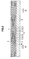
- the low dielectric films 4 are brittle. Therefore, if the grooves 23 are cut in the films 4 by using a blade, the cut surface of the low dielectric films 4 will have many notches and cracks. In view of this, it is recommended that the low dielectric films 4 be cut by the laser beam to make grooves 23. If the grooves 23 are worked by the laser beam, the upper surface of the silicon substrate 1 melts, when irradiated with the laser beam, and molten silicon particles jump and then fall onto the silicon substrate 1. Inevitably, each groove 23 will have an uneven bottom surface as shown in FIG. 5 .
- a width of the groove 23 is 10 to 1000 ⁇ m ⁇ 2 plus a width of the dicing street (a dicing cutter) 22.
- a width of the portion of the sealing film 14 which covers the side surfaces of the low dielectric film wiring line laminated structure portion 3, the passivation film 7 and the protective film 9 is 10 to 1000 ⁇ m.
- the metallic underlayers 11 are formed on the upper surfaces of the connection pad portions 5a of the wiring lines 5 of the uppermost layer exposed via the openings 8, 10 of the passivation film 7 and the protective film 9, on the portions of the upper surface of the semiconductor wafer 21 exposed via the grooves 23, and on the whole upper surface of the protective film 9.
- the metallic underlayers 11 may be formed by an only copper layer formed by electroless plating, an only copper layer formed by sputtering, or a copper layer formed by the sputtering on a thin film layer of titanium or the like formed by the sputtering.
- plating resist films 24 are formed on the upper surfaces of the metallic underlayers 11, and followed by patterning. As a result, openings 25 are formed in portions of the plating resist films 24 corresponding to regions in which the upper layer wiring lines 12 are formed.
- electrolytic plating of copper is performed by use of the metallic underlayers 11 as plating current paths to thereby form the upper layer wiring lines 12 on the upper surfaces of the metallic underlayers 11 in the openings 25 of the plating resist films 24.
- the plating resist films 24 are peeled.
- a plating resist film 26 is formed by depositing and then patterning.
- openings 27 are formed in the plating resist film 26 in portions corresponding to the connection pad portions (regions where the columnar electrodes 13 are formed) of the upper layer wiring lines 12.
- the electrolytic plating of copper is performed by use of the metallic underlayers 11 as the plating current paths, whereby the columnar electrodes 13 each having a height of 50 to 150 ⁇ m are formed on the upper surfaces of the connection pad portions of the upper layer wiring lines 12 in the openings 27 of the plating resist film 26.
- the plating resist film 26 is entirely peeled or removed.
- unnecessary portions of the metallic underlayers 11 are etched and removed by use of the upper layer wiring lines 12 as masks. Consequently, as shown in FIG. 9 , the metallic underlayers 11 only under the upper layer wiring lines 12 are left.
- the sealing film (organic resin film) 14 made of an organic material such as an epoxy-based resin is entirely formed on the upper surfaces of the upper layer wiring lines 12, the columnar electrodes 13 and the protective film 9, as well as on the upper surface of the semiconductor wafer 21 exposed via the grooves 23 so that a thickness of the sealing film 14 is larger than a height of the columnar electrodes 13. Therefore, in this state, the upper surfaces of the columnar electrodes 13 are covered with the sealing film 14.
- the side surfaces of the protective film 9, the passivation film 7 and four layers of the low dielectric films 4 are also entirely covered with the sealing film 14.
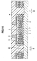
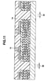
- a portion of the upper surface of the sealing film 14 is appropriately ground to expose the upper surfaces of the columnar electrodes 13 as shown in FIG. 11 . Moreover, the exposed upper surfaces of the columnar electrodes 13 and the upper surface of the sealing film 14 are flattened so that these upper surfaces are on one plane. In flattening this upper surface of the sealing film 14, upper surface portions of the columnar electrodes 13 may be ground together with the upper portion of the sealing film 14 as much as several to ten or more micrometers.
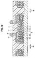
- the solder balls 15 are formed on the upper surfaces of the columnar electrodes 13.
- the sealing film 14 and the semiconductor wafer 21 are cut along the dicing streets 22 in the centers of the grooves 23.
- the grooves 23 have been formed to be wider than the dicing streets 22, there are obtained a plurality of semiconductor devices each having a structure in which, as shown in FIG. 1 , the side surfaces of the low dielectric film wiring line laminated structure portion 3 are covered with the sealing film 14, and further the side surfaces of the passivation film 7 and the upper surface and the side surfaces of the protective film 9 are also covered with the sealing film 14.
- the exposed part of the upper surface of the semiconductor wafer 21 is shown like a bottom portion of the groove 23, but the upper surface of the semiconductor wafer 21 may be partially removed by a laser beam to form the groove 23, so that the bottom portion of the groove 23 may be below the upper surface of the semiconductor wafer 21. If an insulating film such as a field oxide film is formed on the upper surface of the semiconductor wafer 21, the upper surface of this field oxide film or an intermediate portion of a film thickness thereof may be the bottom portion of the groove 23, and the bottom portion of the groove 23 may be positioned above the upper surface of the semiconductor wafer 21.
- an insulating film such as a field oxide film
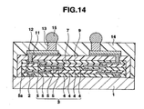
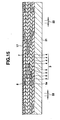
- FIG. 14 shows a sectional view of a semiconductor device as a first embodiment of the present invention.
- This semiconductor device is different from the semiconductor device shown in FIG. 1 in that the upper surface and the side surfaces of the passivation film 7 and the side surfaces of the low dielectric film wiring line laminated structure portion 3 are covered with the protective film 9, and the side surfaces of the protective film 9 is covered with the sealing film 14.
- the water-soluble protective film 17 made of water-soluble polymers such as polyvinyl alcohol (PVA) or polyacrylamide (PAM), is formed on the upper surface of the passivation film 7 and the connecting pad portions 5a of the wiring lines 5 of the uppermost layer, which are exposed via the opening 8 of the passivation film 7, by a screen printing process, a spin coating process or the like.
- PVA polyvinyl alcohol
- PAM polyacrylamide
- the grooves 23 are formed in the water soluble protective film 17, the passivation film 7 and four layers of the low dielectric films 4 in regions of the dicing streets 22 and regions on opposite sides of the streets.
- the low dielectric films 4 melt and scatter as low dielectric film pieces.
- the scattered low dielectric film pieces drop on and stick into the upper surface of the water soluble protective film 17, not the upper surface of the passivation film 7.
- the water soluble protective film 17 is washed with water and removed, the low dielectric film pieces stuck into the upper surface of the water soluble protective film 17 are also removed simultaneously. In this case also, if the scattered low dielectric film pieces are sucked by evacuation, the water soluble protective film 17 may be unnecessary.
- the protective film (organic resin film) 9 made of an organic material such as a polyimide-based resin is formed on the upper surfaces of the connection pad portions 5a of the wiring lines 5 of the uppermost layer exposed via the openings 8 of the passivation film 7, on the upper surface of the passivation film 7, and on the upper surfaces of portions of the semiconductor wafer 21 exposed via the grooves 23. It is preferable that the upper surface of the passivation film 7 and the protective film 9 formed in the grooves 23 have substantially flat surfaces.
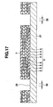
- grooves 23a slightly narrower than the aforementioned grooves 23 are formed in the protective film 9 in the regions of the dicing streets 22 and the regions on opposite sides of the streets, and openings 8 and 10 are formed in portions of the passivation film 7 and the protective film 9 corresponding to the connecting pad portions 5a of the wiring lines 5 in the uppermost layer. Since the subsequent steps are similar to the steps of FIG. 7 et seq. of the first example, description thereof is omitted.
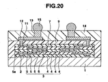
- FIG. 20 shows a sectional view of a semiconductor device as a second embodiment of the present invention.
- the second embodiment is different from the semiconductor device shown in FIG. 14 in that the protective film (organic resin film) 9 which covers the upper surface and the side surfaces of the passivation film 7 and the side surfaces of the low dielectric film wiring line laminated structure portions 3 is extended to the same plane as that of the side surface of the silicon substrate 1.
- the protective film (organic resin film) 9 which covers the upper surface and the side surfaces of the passivation film 7 and the side surfaces of the low dielectric film wiring line laminated structure portions 3 is extended to the same plane as that of the side surface of the silicon substrate 1.
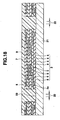
- the groove 23 is completely filled with a part of the protective film 9, as shown in FIG. 18 , so that the groove 23a as shown in FIG. 19 may not be formed. In this case, therefore, the sealing film 14, the protective film 9 and the semiconductor wafer 21 are cut along the dicing streets 22 in the last step.
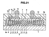
- FIG. 21 is a sectional view of a semiconductor device .
- This semiconductor device is different from the semiconductor device shown in FIG. 1 in that the outer side surfaces 9a of the protective film 9 are located inward from the outer side surfaces of the low dielectric film wiring line laminated structure portion 3 and the passivation film 7.
- the protective film 9 is formed on the passivation film 7 to be smaller than the passivation film 7 in a plane size.
- each of the outer side surfaces of the passivation film 7 and each of the low dielectric film wiring line laminated structure portion 3 substantially form one plane (vertical plane in FIG. 21 ).
- the protective film (organic resin film) 9 is formed on the entire surface of the passivation film 7. Then, the protective film 9 is patterned by means of photolithography, thereby forming the protective film as shown in FIG. 21 .
- the patterning of the protective film 9 is carried out such that a side surface 9a may not reach the dicing line 22.
- the side surface 9a of the protective film 9 is deviated from the side surfaces of the passivation film 7 and the low dielectric film wiring line limited structure portion 3 by a distance greater than a positioning deviation that may occur in the next step of laser radiation.
- the water soluble protective film may be formed on the entire surface, if necessary, and laser beams are applied to the passivation film 7 and the low dielectric film wiring line laminated structure portion 3, making grooves 23.
- the protective film 9 is formed before the protective film 9 is formed.
- the laser beams are applied to the passivation film 7 and the low dielectric film 4, thereby forming the grooves 23.
- the protective film 9 is patterned.
- the protective film 9 is formed on the entire surface of the passivation film 7 including the insides of the grooves 23 by spin coating or the like.
- the protective film 9 is patterned by means of photolithography so as to remove those parts of the protective film 9 in the grooves 23 and peripheries of the passivation film 23, thereby forming the protective film as shown in FIG. 21 .
- the passivation film 7 and the low dielectric film 4 are processed with the laser beams, and the protective film 9 is not. Therefore, this method is particularly effective in the case where the protective film 9 is made of a material, such as a polyimide-based resin, which easily absorbs laser energy and cannot be easily cut by radiation of laser beams.
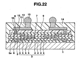
- FIG. 22 is a sectional view of a semiconductor device .
- This semiconductor device is different from the semiconductor device shown in FIG. 21 in that the outer side surfaces of the passivation film 7 are located inward from those of the protective film 9.
- the passivation film 7 is formed on the low dielectric film wiring line laminated structure portion 3 to be smaller than the protective film 9 in a plane size, and the protective film 9 has side portions downwardly extending to cover the side surfaces of the passivation film 7.
- the passivation film 7 is formed on the overall surface of the low dielectric film 4 of the uppermost layer, as shown in FIG. 2 . Then, the passivation film 7 is patterned by means of photolithography. Thereafter, the protective film 9 is formed on the passivation film 7 and parts of the low dielectric film 4 of the uppermost layer which are not covered by the passivation film 7. Thereafter, the protective film 9 is patterned by means of photolithography. Then, if necessary, the water soluble protective film may be formed on the entire surface, and the low dielectric film 4 is processed by radiation of laser beams, thereby forming grooves 23.
- the low dielectric film 4 is processed with laser beams, and the passivation film 7 and the protective film 9 are not. Optimal laser-beam process conditions can therefore be set for the processing of the low dielectric film 4. Hence, the low dielectric film 4 can be processed efficiently with high precision.
- the passivation film 7 may be of the same size as the protective film 9, so that the side surfaces of the passivation film 7 and the side surfaces of the protective film 9 form substantially the same plane.
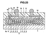
- FIG. 23 is a sectional view of a semiconductor device .
- This semiconductor device is different from the semiconductor device shown in FIG. 21 in that the low dielectric film wiring line laminated structure portion 3 has a lower passivation film 16 between the uppermost wiring line 5 and the uppermost low dielectric film 4.
- the upper passivation film 7 and the lower passivation film 16 may be formed of the same inorganic material, such as silicon oxide.
- the passivation film 7 may be formed of silicon nitride, while the lower passivation film 16 may be formed of silicon oxide.
- the metallic underlayers 11 may be formed on the entire upper surface of the protective film 9.
- the upper wiring lines 12 and the columnar electrodes 13 may be formed by electrolytic plating.
- unnecessary portions of the metallic underlayers 11 may be etched and removed by use of the upper layer wiring lines 12 as masks.
- the water soluble protective film may be formed on the entire surface, if necessary, and laser beams are applied to the protective film 9, the passivation film 7 and the low dielectric film 4, making grooves 23. In this case, if the water soluble protective film is removed after forming the grooves 23, the structure as shown in FIG. 9 can be obtained.
- the uppermost low dielectric film 4 of the low dielectric film wiring line limited structure portion 3 may be a lower passivation film.
- the low dielectric film wiring line limited structure portion 3 may have a lower passivation film formed between the uppermost wiring line 5 and the second uppermost wiring line 5.
- the passivation film 7 and the lower passivation film may be formed of the same inorganic material, such as silicon oxide.
- the passivation film 7 may be formed of silicon nitride, while the lower passivation film may be formed of silicon oxide.
- the upper wiring lines 12 are formed on the protective film 9 and the columnar electrodes 13 are formed on the connection pad portion on the upper wiring lines 12.
- this is applicable to a structure in which only the connection pad portion is formed on the protective film 9 and bump electrodes for external connection, such as solder balls 15, are formed on the connection pad portion.
- the low dielectric film wiring line laminated structure portion having a laminated structure of the low dielectric films, which has a relative dielectric constant of 3.0 or lower and a glass transition temperature of 400°C or higher, and the wiring lines are provided in regions excluding the peripheral portions of the semiconductor substrate.
- the side surfaces of the low dielectric film wiring line laminated structure portion are covered by one of the insulating film formed of organic resin or the sealing film. Therefore, the problem of peeling of the low dielectric films can be significantly avoided.
Description
- The present invention relates to a semiconductor device and a method for manufacturing the same, and particularly a semiconductor device having wiring lines on a low dielectric film.
- As semiconductor devices to be mounted on small-sized electronic devices represented by portable electronic devices and the like, there are known chip size packages (CSPs) each having dimensions substantially equal to that of a semiconductor substrate. Among the CSPs, a CSP in which packaging is completed in a wafer state and which is separated into individual semiconductor devices by dicing is also referred to as a wafer level package (WLP).
- In the conventional semiconductor device as described above (refer to, for example, Jpn. Pat. Appln. KOKAI Publication No.
2004-349461 - Among such semiconductor devices as described above, there is a device in which an interlayer insulating film wiring line laminated structure portions each including a laminated structure of interlayer insulating films and the wiring lines is provided between the semiconductor substrate and the insulating film. In this device, when an interval between the wiring lines of the interlayer insulating film wiring line laminated structure portion decreases with miniaturization of the semiconductor devices, a capacity between the wiring lines increases, with the result that a delay of a signal which transmits through the wiring lines increases.
- To improve this point, as a material of the interlayer insulating film, much attention is paid to a low dielectric material such as a low-k material having a dielectric constant lower than a dielectric constant of 4.2 to 4.0 of silicon oxide which is generally used as the material of the interlayer insulating film. Examples of the low-k material include SiOC obtained by doping silicon oxide (SiO2) with carbon (C), and SiOCH further containing H. To further lower the dielectric constant, air-containing porous type low dielectric films are also being investigated.
- In the above semiconductor device including the low dielectric film, especially the low dielectric film represented by the porous type low dielectric film having a hollow structure has a small mechanical strength and is easily influenced by moisture. As a result, there is a problem that the low dielectric film easily peels from an underlayer.
-
EP-A-1 298 725 relates to a semiconductor device of a multi-wiring structure, particularly, to the structure of an insulating film within the same wiring layer. -
US 2002/024145 A1 discloses a semiconductor device using a fluorinated silicate glass film as an interlayer metal dielectric film. -
EP-A-1 737 037 relates to a method for fabricating a circuitry component. The method comprises the steps of providing a semiconductor wafer, a first metal layer, and a first polymer layer. -
US-B1-6 559 548 relates to a wiring structure of a semiconductor device comprising a first insulating layer, a wiring layer, a second insulating layer, a first via plug, an electrode pad and a second via plug. -
US 2005/170641 A1 discloses a method for forming a buried wiring in a low-k dielectric film. -
US 2002/100984 A1 relates to a semiconductor device having wirings formed in wiring grooves and a connection member formed integrally with the wirings in via holes for connecting the wirings and lower layer wirings thereof. - An object of the present invention is to provide a semiconductor device capable of significantly avoiding a problem of peeling of a low dielectric film, and a method for manufacturing the same.
- A semiconductor device according to one aspect of the present invention comprises a semiconductor substrate and a low dielectric film wiring line laminated structure portion which is provided on one surface of the semiconductor substrate. The low dielectric film wiring line laminated structure portion has a laminated structure including a plurality of low dielectric films and a plurality of wiring lines, each of the low dielectric films having a relative dielectric constant of 3.0 or lower and a glass transition temperature of 400°C or higher. An insulating film is formed at least on the low dielectric film wiring line laminated structure portion. On the insulating film, there are provided a connection pad portion for an electrode so as to be connected to a connection pad portion of an uppermost wiring line of the low dielectric film wiring line laminated structure portion, a bump electrode for external connection, provided on the connection pad portion for the electrode, and a sealing film made of an organic resin and provided at least on a part of the insulating film which surrounds the pump electrode for the external connection. Side surfaces of the low dielectric film wiring line laminated structure portion are covered with one of the insulating film and the sealing film.
- A method for manufacturing a semiconductor device according to another aspect of the present invention comprises preparing a semiconductor wafer, on one surface of which a low dielectric film wiring line laminated structure portion is formed, the low dielectric film wiring line laminated structure portion including low dielectric films and wiring lines, the low dielectric films having a relative dielectric constant of 3.0 or lower and a glass transition temperature of 400°C or higher. In the next, parts of the low dielectric film wiring line laminated structure portion in regions above dicing streets and regions on opposite sides of the dicing streets are removed by applying laser beams, thereby forming a groove exposing side surfaces of the low dielectric film wiring line laminated structure portion. Thereafter, an organic resin film covering the side surfaces of the low dielectric film wiring line laminated structure portion is formed. Then, the organic resin film and the semiconductor wafer are cut along the dicing streets, thereby obtaining a plurality of semiconductor devices.
-
-
FIG. 1 is a sectional view of a semiconductor device as a first example -
FIG. 2 is a sectional view of an assembly first prepared during manufacturing of the semiconductor device shown inFIG. 1 ; -
FIG. 3 is a sectional view of an assembly in a step subsequent toFIG. 2 ; -
FIG. 4 is a sectional view of an assembly in a step subsequent toFIG. 3 ; -
FIG. 5 is a sectional view of an assembly in a step subsequent toFIG. 4 ; -
FIG. 6 is a sectional view of an assembly in a step subsequent toFIG. 5 ; -
FIG. 7 is a sectional view of an assembly in a step subsequent toFIG. 6 ; -
FIG. 8 is a sectional view of an assembly in a step subsequent toFIG. 7 ; -
FIG. 9 is a sectional view of an assembly in a step subsequent toFIG. 8 ; -
FIG. 10 is a sectional view of an assembly in a step subsequent toFIG. 9 ; -
FIG. 11 is a sectional view of an assembly in a step subsequent toFIG. 10 ; -
FIG. 12 is a sectional view of an assembly in a step subsequent toFIG. 11 ; -
FIG. 13 is a sectional view of an assembly in a step subsequent toFIG. 12 ; -
FIG. 14 is a sectional view of a semiconductor device as a first embodiment of the present invention; -
FIG. 15 is a sectional view of an assembly in a predetermined step during manufacturing of the semiconductor device shown inFIG. 14 ; -
FIG. 16 is a sectional view of an assembly in a step subsequent toFIG. 15 ; -
FIG. 17 is a sectional view of an assembly in a step subsequent toFIG. 16 ; -
FIG. 18 is a sectional view of an assembly in a step subsequent toFIG. 17 ; -
FIG. 19 is a sectional view of an assembly in a step subsequent toFIG. 18 ; -
FIG. 20 is a sectional view of a semiconductor device as a second embodiment of the present invention; -
FIG. 21 is a sectional view of a semiconductor device ; -
FIG. 22 is a sectional view of a semiconductor device ; and -
FIG. 23 is a sectional view of a semiconductor device . -
FIG. 1 shows a sectional view of a semiconductor device as a first example. This semiconductor device includes a silicon substrate (a semiconductor substrate) 1. On the upper surface of thesilicon substrate 1, a number of active semiconductor elements, such as transistors, are provided (not shown). In a peripheral portion of the upper surface of thesubstrate 1, a number ofconnection pads 2 made of an aluminum-based metal or the like are electrically connected to the respective semiconductor elements, although the figure shows only two pads. Theconnection pads 2 are input and/or output terminals of each semiconductor element, and/or a power supply terminal. - On the upper surface of the
silicon substrate 1, excluding peripheral portions outside theconnection pads 2, a low dielectric film/wiring line/laminated structure portion 3 is provided. Thelaminated structure portion 3 has a structure in which there are alternately laminated a plurality of layers, for example, four layers of lowdielectric films 4 and the same number of layers ofwiring lines 5 made of copper or an aluminum-based metal or the like. - Examples of a material of the low
dielectric films 4 include a polysiloxane-based material having an Si-O bond and an Si-H bond (HSQ:Hydrogen silsesquioxane having a relative dielectric constant of 3.0), a polysiloxane-based material having an Si-O bond and an Si-CH3 bond (MSQ:Methyl silsesquioxane having a relative dielectric constant of 2.7-2.9), carbon-doped silicon oxide (SiOC having a relative dielectric constant of 2.7-2.9) and an organic polymer-based low-k material. The materials having a relative dielectric constant of 3.0 or lower and a glass transition temperature of 400°C or higher can be used. - Examples of the organic polymer-based low-k material include "SiLK (having a relative dielectric constant of 2.6)" produced by Dow Chemical Company and "FLARE (having a relative dielectric constant of 2.8)" produced by Honeywell Electronic Materials Company. The glass transition temperature of 400°C or higher is a condition for tolerance to a temperature in a manufacturing step or steps to be described later. A porous type of each of the above materials may also be used.
- Besides the above, the material of the low
dielectric films 4 may also be a material which has a relative dielectric constant higher than 3.0 in a normal condition, but can have a relative dielectric constant of 3.0 or lower and a glass transition temperature of 400°C or higher when it becomes porous. For example, fluorinated silicate glass (FSG having a relative dielectric constant of 3.5-3.7), boron-doped silicate glass (BSG having a relative dielectric constant of 3.5) or silicon oxide (having a relative dielectric constant of 4.0-4.2) may be used. - In the low dielectric film wiring line laminated
structure portion 3, thewiring lines 5 between the lowdielectric films 4 are electrically connected to each other through holes formed in thefilms 4. One end portion of thewiring line 5 of the lowermost layer is electrically connected to theconnection pad 2 via anopening 6 formed in thelow dielectric film 4 of the lowermost layer.Connection pad portions 5a of thewiring lines 5 of an uppermost layer are arranged on an upper surface peripheral portion of thelow dielectric film 4 of the uppermost layer. - A
passivation film 7 made of an inorganic material such as silicon oxide is provided on the upper surfaces of theuppermost wiring lines 5 and the lowdielectric films 4 of the uppermost layer.Openings 8 are formed through thepassivation film 7 in portions corresponding to theconnection pad portions 5a of thewiring lines 5 of the uppermost layer. On the upper surface of thepassivation film 7, there is provided a protective film (insulating film) 9 made of an organic material containing polyimide, epoxy, phenol, bismaleimide, acryl, synthetic rubber, polybenzoxide or the like as a main component.Openings 10 are formed through theprotective film 9 in portions corresponding to theopenings 8 of thepassivation film 7. - On the upper surface of the
protective film 9,metallic underlayers 11 made of copper or the like are provided. On the whole upper surface of each of themetallic underlayers 11, an upperlayer wiring line 12 made of copper is provided. End portions of the upperlayer wiring line 12 and themetallic underlayers 11, are connected to theconnection pad portions 5a of thewiring lines 5 of the uppermost layer via theopenings passivation film 7 and theprotective film 9. On the upper surfaces of connection pad portions (connecting pad portions for electrodes) of the upperlayer wiring lines 12, there are provided columnar electrodes (bump electrodes for external connection) 13 made of copper. - On the upper surfaces of the upper
layer wiring liners 12 and theprotective film 9, and the upper surface of the peripheral portion of thesilicon substrate 1, there is provided asealing film 14 made of an organic material such as an epoxy-based resin so that the upper surface of the sealing film and the upper surfaces of thecolumnar electrodes 13 are on one plane. In this state, the side surfaces of the low dielectric film wiring line laminatedstructure portion 3, thepassivation film 7 and theprotective film 9 form substantially one plane and are entirely covered with the sealingfilm 14.Solder balls 15 are provided on the upper surfaces of thecolumnar electrodes 13. - As described above, in this semiconductor device, a region on the
silicon substrate 1 except the peripheral portion is provided with the low dielectric film wiring line laminated structure portion orstructure portions 3 each including the laminated structure of the lowdielectric films 4 and thewiring lines 5, and the side surfaces of the low dielectric film wiring line laminatedstructure portion 3, thepassivation film 7 and theprotective film 9 are covered with the sealingfilm 14. Therefore, the low dielectric film wiring line laminatedstructure portion 3 does not easily peel from thesilicon substrate 1. - Next, one example of a method for manufacturing the semiconductor device mentioned above will be described. First, as shown in
FIG. 2 , an assembly is prepared, in which on a silicon substrate (hereinafter referred to as a semiconductor wafer 21) of a wafer state, there are arranged theconnection pads 2 and the low dielectric film wiring line laminatedstructure portions 3 each including four layers of lowdielectric films 4 andwiring lines 5. In the assembly, thepassivation film 7 is provided on thelaminated stricture portions 3, and the centers of theconnection pad portions 5a of thewiring lines 5 of the uppermost layer are exposed via theopenings 8 provided in thepassivation film 7. - Examples of a low
dielectric film material 4 may be those, including a porous type, as described above, which have a relative dielectric constant of 3.0 or lower and a glass transition temperature of 400°C or higher. It is to be noted that regions denoted withreference numeral 22 inFIG. 2 are regions corresponding to dicing streets. - Next, as shown in
FIG. 3 , by a screen printing process, a spin coating process or the like, theprotective film 9 made of an organic material such as a polyimide-based resin is formed on the upper surface of thepassivation film 7 and the upper surfaces of theconnection pad portions 5a of thewiring lines 5 of the uppermost layer exposed via theopenings 8 of thepassivation film 7. Then, as shown inFIG. 4 , a water-solubleprotective film 17, made of water-soluble polymers such as polyvinyl alcohol (PVA) or polyacrylamide (PAM), is formed on the upper surface of theprotective film 9 by a screen printing process, a spin coating process or the like. - Next, as shown in
FIG. 5 , by laser processing which emits a laser beam, there are removed portions of the water solubleprotective film 17, theprotective film 9, thepassivation film 7 and four layers of the lowdielectric films 4 positioned in regions of the dicingstreets 22 and regions on opposite sides of the streets to formlatticed grooves 23. Further, theopenings passivation film 7 and the water solubleprotective film 17 in portions corresponding to theconnection pad portions 5a of thewiring lines 5 of the uppermost layer. - In this process, when the laser beam is radiated on the low
dielectric films 4, the lowdielectric films 4 melt and scatter as low dielectric film pieces. The scattered low dielectric film pieces drop on and stick into the upper surface of the water solubleprotective film 17, not the upper surface of theprotective film 9. Then, when the water solubleprotective film 17 is washed with water and removed, the low dielectric film pieces stuck into the upper surface of the water solubleprotective film 17 are also removed simultaneously. If the scattered low dielectric film pieces are sucked by evacuation, the water solubleprotective film 17 may be unnecessary. - The low
dielectric films 4 are brittle.
Therefore, if thegrooves 23 are cut in thefilms 4 by using a blade, the cut surface of the lowdielectric films 4 will have many notches and cracks. In view of this, it is recommended that the lowdielectric films 4 be cut by the laser beam to makegrooves 23. If thegrooves 23 are worked by the laser beam, the upper surface of thesilicon substrate 1 melts, when irradiated with the laser beam, and molten silicon particles jump and then fall onto thesilicon substrate 1. Inevitably, eachgroove 23 will have an uneven bottom surface as shown inFIG. 5 . - In this state, that is, in the state where the water soluble
protective film 17 has been removed, as shown inFIG. 6 , the upper surface of thesemiconductor wafer 21 in the regions of the dicingstreets 22 and the regions on opposite sides of the streets is exposed via thegrooves 23. Moreover, portions of the four layers of the lowdielectric films 4, thepassivation film 7 and theprotective film 9 laminated on thesemiconductor wafer 21 are separated from one another by thegrooves 23. In consequence, a plurality of low dielectric film wiring line laminatedstructure portions 3 independent of one another are formed on thewafer 21, as shown inFIG. 1 . - As one example, a width of the
groove 23 is 10 to 1000 µm × 2 plus a width of the dicing street (a dicing cutter) 22. As a result in the completed device shown inFIG. 1 , a width of the portion of the sealingfilm 14 which covers the side surfaces of the low dielectric film wiring line laminatedstructure portion 3, thepassivation film 7 and theprotective film 9 is 10 to 1000 µm. - Next, as shown in
FIG. 7 , themetallic underlayers 11 are formed on the upper surfaces of theconnection pad portions 5a of thewiring lines 5 of the uppermost layer exposed via theopenings passivation film 7 and theprotective film 9, on the portions of the upper surface of thesemiconductor wafer 21 exposed via thegrooves 23, and on the whole upper surface of theprotective film 9. In this case, themetallic underlayers 11 may be formed by an only copper layer formed by electroless plating, an only copper layer formed by sputtering, or a copper layer formed by the sputtering on a thin film layer of titanium or the like formed by the sputtering. - Next, plating resist
films 24 are formed on the upper surfaces of themetallic underlayers 11, and followed by patterning. As a result, openings 25 are formed in portions of the plating resistfilms 24 corresponding to regions in which the upperlayer wiring lines 12 are formed. Next, electrolytic plating of copper is performed by use of themetallic underlayers 11 as plating current paths to thereby form the upperlayer wiring lines 12 on the upper surfaces of themetallic underlayers 11 in the openings 25 of the plating resistfilms 24. Next, the plating resistfilms 24 are peeled. - Next, as shown in
FIG. 8 , on the upper surfaces of themetallic underlayers 11 and the upperlayer wiring lines 12, a plating resistfilm 26 is formed by depositing and then patterning. Thus, in this case,openings 27 are formed in the plating resistfilm 26 in portions corresponding to the connection pad portions (regions where thecolumnar electrodes 13 are formed) of the upper layer wiring lines 12. Next, the electrolytic plating of copper is performed by use of themetallic underlayers 11 as the plating current paths, whereby thecolumnar electrodes 13 each having a height of 50 to 150 µm are formed on the upper surfaces of the connection pad portions of the upperlayer wiring lines 12 in theopenings 27 of the plating resistfilm 26. Next, the plating resistfilm 26 is entirely peeled or removed. Then, unnecessary portions of themetallic underlayers 11 are etched and removed by use of the upperlayer wiring lines 12 as masks. Consequently, as shown inFIG. 9 , themetallic underlayers 11 only under the upperlayer wiring lines 12 are left. - Next, as shown in
FIG. 10 , by a screen printing process, a spin coating process or the like, the sealing film (organic resin film) 14 made of an organic material such as an epoxy-based resin is entirely formed on the upper surfaces of the upperlayer wiring lines 12, thecolumnar electrodes 13 and theprotective film 9, as well as on the upper surface of thesemiconductor wafer 21 exposed via thegrooves 23 so that a thickness of the sealingfilm 14 is larger than a height of thecolumnar electrodes 13. Therefore, in this state, the upper surfaces of thecolumnar electrodes 13 are covered with the sealingfilm 14. The side surfaces of theprotective film 9, thepassivation film 7 and four layers of the lowdielectric films 4 are also entirely covered with the sealingfilm 14. - Next, a portion of the upper surface of the sealing
film 14 is appropriately ground to expose the upper surfaces of thecolumnar electrodes 13 as shown inFIG. 11 . Moreover, the exposed upper surfaces of thecolumnar electrodes 13 and the upper surface of the sealingfilm 14 are flattened so that these upper surfaces are on one plane. In flattening this upper surface of the sealingfilm 14, upper surface portions of thecolumnar electrodes 13 may be ground together with the upper portion of the sealingfilm 14 as much as several to ten or more micrometers. - Next, as shown in
FIG. 12 , thesolder balls 15 are formed on the upper surfaces of thecolumnar electrodes 13. Next, as shown inFIG. 13 , the sealingfilm 14 and thesemiconductor wafer 21 are cut along the dicingstreets 22 in the centers of thegrooves 23. As described above, since thegrooves 23 have been formed to be wider than the dicingstreets 22, there are obtained a plurality of semiconductor devices each having a structure in which, as shown inFIG. 1 , the side surfaces of the low dielectric film wiring line laminatedstructure portion 3 are covered with the sealingfilm 14, and further the side surfaces of thepassivation film 7 and the upper surface and the side surfaces of theprotective film 9 are also covered with the sealingfilm 14. - In the above embodiment, the exposed part of the upper surface of the
semiconductor wafer 21 is shown like a bottom portion of thegroove 23, but the upper surface of thesemiconductor wafer 21 may be partially removed by a laser beam to form thegroove 23, so that the bottom portion of thegroove 23 may be below the upper surface of thesemiconductor wafer 21. If an insulating film such as a field oxide film is formed on the upper surface of thesemiconductor wafer 21, the upper surface of this field oxide film or an intermediate portion of a film thickness thereof may be the bottom portion of thegroove 23, and the bottom portion of thegroove 23 may be positioned above the upper surface of thesemiconductor wafer 21. -
FIG. 14 shows a sectional view of a semiconductor device as a first embodiment of the present invention. This semiconductor device is different from the semiconductor device shown inFIG. 1 in that the upper surface and the side surfaces of thepassivation film 7 and the side surfaces of the low dielectric film wiring line laminatedstructure portion 3 are covered with theprotective film 9, and the side surfaces of theprotective film 9 is covered with the sealingfilm 14. - As one example of manufacturing this semiconductor device, an assembly shown in
FIG. 2 is prepared. Then, as shown inFIG. 15 , the water-solubleprotective film 17, made of water-soluble polymers such as polyvinyl alcohol (PVA) or polyacrylamide (PAM), is formed on the upper surface of thepassivation film 7 and the connectingpad portions 5a of thewiring lines 5 of the uppermost layer, which are exposed via theopening 8 of thepassivation film 7, by a screen printing process, a spin coating process or the like. - Thereafter, as shown in
FIG. 16 , by laser processing which emits a laser beam, thegrooves 23 are formed in the water solubleprotective film 17, thepassivation film 7 and four layers of the lowdielectric films 4 in regions of the dicingstreets 22 and regions on opposite sides of the streets. In this process also, when the laser beam is radiated on the lowdielectric films 4, the lowdielectric films 4 melt and scatter as low dielectric film pieces. The scattered low dielectric film pieces drop on and stick into the upper surface of the water solubleprotective film 17, not the upper surface of thepassivation film 7. Then, when the water solubleprotective film 17 is washed with water and removed, the low dielectric film pieces stuck into the upper surface of the water solubleprotective film 17 are also removed simultaneously. In this case also, if the scattered low dielectric film pieces are sucked by evacuation, the water solubleprotective film 17 may be unnecessary. - In this state, that is, in the state where the water soluble protective film is removed as shown in
FIG. 17 , the upper surfaces of thesemiconductor wafer 21 in the dicingstreets 22 and the regions on opposite sides of the streets are exposed via thegrooves 23. Moreover, units which are laminated on thesemiconductor wafer 21 and which are each constituted of four layers of the lowdielectric films 4 and thepassivation film 7 are separated from one another along thegrooves 23. In consequence, a plurality of low dielectric film wiring line laminatedstructure portions 3 shown inFIG. 14 are formed on thesemiconductor wafer 21. - Next, as shown in
FIG. 18 , by a screen printing process, a spin coating process or the like, the protective film (organic resin film) 9 made of an organic material such as a polyimide-based resin is formed on the upper surfaces of theconnection pad portions 5a of thewiring lines 5 of the uppermost layer exposed via theopenings 8 of thepassivation film 7, on the upper surface of thepassivation film 7, and on the upper surfaces of portions of thesemiconductor wafer 21 exposed via thegrooves 23. It is preferable that the upper surface of thepassivation film 7 and theprotective film 9 formed in thegrooves 23 have substantially flat surfaces. - Next, as shown in
FIG. 19 , by laser processing which emits a laser beam or photolithography,grooves 23a slightly narrower than theaforementioned grooves 23 are formed in theprotective film 9 in the regions of the dicingstreets 22 and the regions on opposite sides of the streets, andopenings passivation film 7 and theprotective film 9 corresponding to the connectingpad portions 5a of thewiring lines 5 in the uppermost layer. Since the subsequent steps are similar to the steps ofFIG. 7 et seq. of the first example, description thereof is omitted. -
FIG. 20 shows a sectional view of a semiconductor device as a second embodiment of the present invention. The second embodiment is different from the semiconductor device shown inFIG. 14 in that the protective film (organic resin film) 9 which covers the upper surface and the side surfaces of thepassivation film 7 and the side surfaces of the low dielectric film wiring line laminatedstructure portions 3 is extended to the same plane as that of the side surface of thesilicon substrate 1. - To produce the above semiconductor device, the
groove 23 is completely filled with a part of theprotective film 9, as shown inFIG. 18 , so that thegroove 23a as shown inFIG. 19 may not be formed. In this case, therefore, the sealingfilm 14, theprotective film 9 and thesemiconductor wafer 21 are cut along the dicingstreets 22 in the last step. -
FIG. 21 is a sectional view of a semiconductor device . This semiconductor device is different from the semiconductor device shown inFIG. 1 in that theouter side surfaces 9a of theprotective film 9 are located inward from the outer side surfaces of the low dielectric film wiring line laminatedstructure portion 3 and thepassivation film 7. In other words, theprotective film 9 is formed on thepassivation film 7 to be smaller than thepassivation film 7 in a plane size. In this case, each of the outer side surfaces of thepassivation film 7 and each of the low dielectric film wiring line laminatedstructure portion 3 substantially form one plane (vertical plane inFIG. 21 ). - An example of the method for manufacturing the semiconductor device will be described. For example, as shown in
FIG. 3 , the protective film (organic resin film) 9 is formed on the entire surface of thepassivation film 7. Then, theprotective film 9 is patterned by means of photolithography, thereby forming the protective film as shown inFIG. 21 . The patterning of theprotective film 9 is carried out such that aside surface 9a may not reach the dicingline 22. Theside surface 9a of theprotective film 9 is deviated from the side surfaces of thepassivation film 7 and the low dielectric film wiring linelimited structure portion 3 by a distance greater than a positioning deviation that may occur in the next step of laser radiation. Thereafter, the water soluble protective film may be formed on the entire surface, if necessary, and laser beams are applied to thepassivation film 7 and the low dielectric film wiring line laminatedstructure portion 3, makinggrooves 23. - Another example of the method for manufacturing the semiconductor device will be described. In this example, as shown in
FIG. 17 , before theprotective film 9 is formed, the laser beams are applied to thepassivation film 7 and thelow dielectric film 4, thereby forming thegrooves 23. Then, as shown inFIG. 18 , after the laser beams are applied to form thegrooves 23, theprotective film 9 is patterned. Next, theprotective film 9 is formed on the entire surface of thepassivation film 7 including the insides of thegrooves 23 by spin coating or the like. Then, theprotective film 9 is patterned by means of photolithography so as to remove those parts of theprotective film 9 in thegrooves 23 and peripheries of thepassivation film 23, thereby forming the protective film as shown inFIG. 21 . - In both the above examples of the method for manufacturing the semiconductor device, the
passivation film 7 and thelow dielectric film 4 are processed with the laser beams, and theprotective film 9 is not. Therefore, this method is particularly effective in the case where theprotective film 9 is made of a material, such as a polyimide-based resin, which easily absorbs laser energy and cannot be easily cut by radiation of laser beams. -
FIG. 22 is a sectional view of a semiconductor device . This semiconductor device is different from the semiconductor device shown inFIG. 21 in that the outer side surfaces of thepassivation film 7 are located inward from those of theprotective film 9. In other words, thepassivation film 7 is formed on the low dielectric film wiring line laminatedstructure portion 3 to be smaller than theprotective film 9 in a plane size, and theprotective film 9 has side portions downwardly extending to cover the side surfaces of thepassivation film 7. - To manufacture this semiconductor device, the
passivation film 7 is formed on the overall surface of thelow dielectric film 4 of the uppermost layer, as shown inFIG. 2 . Then, thepassivation film 7 is patterned by means of photolithography. Thereafter, theprotective film 9 is formed on thepassivation film 7 and parts of thelow dielectric film 4 of the uppermost layer which are not covered by thepassivation film 7. Thereafter, theprotective film 9 is patterned by means of photolithography. Then, if necessary, the water soluble protective film may be formed on the entire surface, and thelow dielectric film 4 is processed by radiation of laser beams, thereby forminggrooves 23. - In the above method for manufacturing the semiconductor device, only the
low dielectric film 4 is processed with laser beams, and thepassivation film 7 and theprotective film 9 are not. Optimal laser-beam process conditions can therefore be set for the processing of thelow dielectric film 4. Hence, thelow dielectric film 4 can be processed efficiently with high precision. It is to be noted that thepassivation film 7 may be of the same size as theprotective film 9, so that the side surfaces of thepassivation film 7 and the side surfaces of theprotective film 9 form substantially the same plane. -
FIG. 23 is a sectional view of a semiconductor device . This semiconductor device is different from the semiconductor device shown inFIG. 21 in that the low dielectric film wiring line laminatedstructure portion 3 has alower passivation film 16 between theuppermost wiring line 5 and the uppermostlow dielectric film 4. - In this case, the
upper passivation film 7 and thelower passivation film 16 may be formed of the same inorganic material, such as silicon oxide. Alternatively, thepassivation film 7 may be formed of silicon nitride, while thelower passivation film 16 may be formed of silicon oxide. - For example, in the first example, after the process shown in
FIG. 3 , themetallic underlayers 11 may be formed on the entire upper surface of theprotective film 9. Then, theupper wiring lines 12 and thecolumnar electrodes 13 may be formed by electrolytic plating. Then, unnecessary portions of themetallic underlayers 11 may be etched and removed by use of the upperlayer wiring lines 12 as masks. Thereafter, the water soluble protective film may be formed on the entire surface, if necessary, and laser beams are applied to theprotective film 9, thepassivation film 7 and thelow dielectric film 4, makinggrooves 23. In this case, if the water soluble protective film is removed after forming thegrooves 23, the structure as shown inFIG. 9 can be obtained. - Referring to
FIG. 21 , for example, the uppermostlow dielectric film 4 of the low dielectric film wiring linelimited structure portion 3 may be a lower passivation film. In other words, the low dielectric film wiring linelimited structure portion 3 may have a lower passivation film formed between theuppermost wiring line 5 and the seconduppermost wiring line 5. - In this case, the
passivation film 7 and the lower passivation film may be formed of the same inorganic material, such as silicon oxide. Alternatively, thepassivation film 7 may be formed of silicon nitride, while the lower passivation film may be formed of silicon oxide. - In the above embodiments and examples, the
upper wiring lines 12 are formed on theprotective film 9 and thecolumnar electrodes 13 are formed on the connection pad portion on the upper wiring lines 12. However, this is applicable to a structure in which only the connection pad portion is formed on theprotective film 9 and bump electrodes for external connection, such assolder balls 15, are formed on the connection pad portion. - As described above, the low dielectric film wiring line laminated structure portion having a laminated structure of the low dielectric films, which has a relative dielectric constant of 3.0 or lower and a glass transition temperature of 400°C or higher, and the wiring lines are provided in regions excluding the peripheral portions of the semiconductor substrate. The side surfaces of the low dielectric film wiring line laminated structure portion are covered by one of the insulating film formed of organic resin or the sealing film. Therefore, the problem of peeling of the low dielectric films can be significantly avoided.
Claims (20)
- A semiconductor device comprising:a semiconductor substrate (1);a low dielectric film wiring line laminated structure portion (3) provided in regions excluding peripheral portions of one surface of the semiconductor substrate (1), and the low dielectric film wiring line laminated structure portion (3) constitutes a laminated structure including a plurality of low dielectric films (4) and a plurality of wiring lines (5), each of the low dielectric films having a relative dielectric constant of 3.0 or lower and a glass transition temperature of 400°C or higher;an insulating film covering the upper surface of the low dielectric film wiring line laminated structure portion (3);a connection pad portion for an electrode, said connection pad portion for an electrode being arranged on said insulating film (9) provided on the low dielectric film wiring line laminated structure portion (3), whereby said connection pad portion for an electrode is connected to a connection pad portion (5a) of an uppermost wiring line (5) of the low dielectric film wiring line laminated structure portion (3);a bump electrode (13) for external connection, provided on the connection pad portion for the electrode; anda sealing film (14) made of an organic resin and provided at least on a part of the insulating film (9) to surround the bump electrode (13) for the external connection,characterized in that the side surfaces of the low dielectric film wiring line laminated structure portion (3) are also covered with the insulating film (9).
- The semiconductor device according to claim 1, further comprising a passivation film (7) made of an inorganic material between the insulating film (9) and the low dielectric film wiring line laminated structure portion (3).
- The semiconductor device according to claim 2, wherein corresponding side surfaces of the insulating film (9), the passivation film (7) and the low dielectric film wiring line laminated structure portion (3) form one plane, and the side surfaces of the insulating film (9), the passivation film (7) and the low dielectric film wiring line laminated structure portion (3) are covered with the sealing film (14).
- The semiconductor device according to claim 2, wherein corresponding side surfaces of the passivation film (7) and the low dielectric film wiring line laminated structure portion (3) form one plane, and the side surfaces of the passivation film (7) and the low dielectric film wiring line laminated structure portion (3) are covered with the insulating film (9).
- The semiconductor device according to claim 2, wherein the side surfaces of the insulating film (9) are located inward from the side surfaces of the low dielectric film wiring line laminated structure portion (3).
- The semiconductor device according to claim 5, wherein the side surfaces of the passivation film (7) are located inward from the corresponding side surfaces of the insulating film (9).
- The semiconductor device according to claim 5, wherein the corresponding side surfaces of the insulating film (9) and the passivation film (7) form one plane.
- The semiconductor device according to claim 1, wherein the low dielectric film wiring line laminated structure portion (3) has a lower passivation film (16) formed between the uppermost wiring line (5) and an uppermost low dielectric film (4).
- The semiconductor device according to any one of claims 1 to 8, wherein the low dielectric film (14) includes one of a polysiloxane-based material having an Si-O bond and an Si-H bond, a polysiloxane-based material having an Si-O bond and an Si-CH3 bond, a carbon-doped silicon oxide and an organic polymer-based low-k material, or a porous type of one of a fluorine-doped silicon oxide, boron-doped silicon oxide and silicon oxide.
- A method of manufacturing a semiconductor device, comprising:preparing a semiconductor wafer (21), on one surface of which a low dielectric film wiring line laminated structure portion (3) is formed, the low dielectric film wiring line laminated structure portion (3) including low dielectric films (4) and wiring lines (5), the low dielectric films having a relative dielectric constant of 3.0 or lower and a glass transition temperature of 400°C or higher; andremoving parts of the low dielectric film wiring line laminated structure portion (3) in regions above dicing streets (22) and regions on opposite sides of the dicing streets by applying laser beams, and forming a groove (23) exposing side surfaces of the low dielectric film wiring line laminated structure portion (3);forming an insulating film (9) covering an upper surface and the side surfaces of the low dielectric film wiring line laminated structure portion (3); and forming a bump electrode (13) for the external connection on the pad connected with a connection pad portion (5a) of an uppermost wiring line (5) of the low dielectric film wiring line laminated structure portion (3),forming a sealing film (14) made of an organic resin on the insulating film (9) to surround the bump electrode (13) for the external connection, andcutting the insulating film (9), the sealing film (14) formed on the insulating film (9) and the semiconductor wafer (21) along the dicing streets (22), thereby obtaining a plurality of semiconductor devices.
- The method for manufacturing a semiconductor device according to claim 10, wherein the forming a groove (23) includes forming a water soluble protective film (17) entirely on the organic resin film (9) before forming the groove (23), and removing the water soluble protective film (17) after forming the groove (23).
- The method for manufacturing a semiconductor device according to claim 10, wherein the forming the organic resin film (9, 14) includes forming an insulating film (9) made of organic resin covering an upper portion of the low dielectric film wiring line laminated structure portion (3).
- The method for manufacturing a semiconductor device according to claim 12, further comprising:forming a connecting pad portion for an electrode on the insulating film (9) so as to be connected to a connection pad portion of an uppermost wiring line (5) of the low dielectric film wiring line laminated structure portion (3); andforming a bump electrode (13) for external connection on the connection pad portion for the electrode.
- The method for manufacturing a semiconductor device according to claim 10, wherein the preparing a semiconductor wafer (21), on one surface of which a low dielectric film wiring line laminated structure portion (3) is formed, includes preparing the low dielectric film wiring line laminated structure portion (3) on which an insulating film (9) made of organic resin is formed, and the forming a groove includes removing parts of the insulating film (9) and the low dielectric film wiring line laminated structure portion (3) in the regions above the dicing streets (22) and the regions on the opposite sides of the dicing streets by applying laser beams and forming the groove (23) exposing side surfaces of the insulating film (9) and the low dielectric film wiring line laminated structure portion (3).
- The method for manufacturing a semiconductor device according to claim 10, wherein the preparing a semiconductor wafer (21), on one surface of which a low dielectric film wiring line laminated structure portion (3) is formed, includes preparing the low dielectric film wiring line laminated structure portion (3) on which a passivation film (7) is formed, and the forming a groove (23) includes removing parts of the passivation film (7) and the low dielectric film wiring line laminated structure portion (3) in the regions above the dicing streets (22) and the regions on the opposite sides of the dicing street, and forming the groove (23) exposing side surfaces of the passivation film (7) and the side surfaces of the low dielectric film wiring line laminated structure portion (3).
- The method for manufacturing a semiconductor device according to claim 15, wherein the forming an organic resin film (9, 14) includes forming an insulating film (9, 14) made of an organic resin covering an upper surface of the passivation film (7) and the side surfaces of the passivation film (7) and the side surfaces of the low dielectric film wiring line laminated structure portion (3) exposed through the groove (23).
- The method for manufacturing a semiconductor device according to claim 16, wherein the forming an insulating film (9, 14) includes patterning the insulating film (9, 14) to prevent the insulating film (9, 14) from extending above the dicing street (22).
- The method for manufacturing a semiconductor device according to claim 17, wherein the forming an insulating film (9, 14) includes forming the insulating film (9) on the low dielectric film wiring line laminated structure portion (3) and in the groove (3) and patterning the insulating film (9) such that side surfaces of the insulating film (9) are located inward from the side surfaces of the low dielectric film wiring line laminated structure portion (3).
- The method for manufacturing a semiconductor device according to claim 10, wherein the preparing a semiconductor wafer (21), on one surface of which a low dielectric film wiring line laminated structure portion (3) is formed, includes patterning the insulating film (14) on the low dielectric film wiring line laminated structure portion (3) to prevent the insulating film (14) made of an organic resin from extending above the dicing street (22).
- The method for manufacturing a semiconductor device according to claim 10, further comprising:forming a connecting pad portion for an electrode on the insulating film (9) so as to be connected to a connection pad portion of an uppermost wiring line (5) of the low dielectric film wiring line laminated structure portion (3); andforming a bump electrode (13) for external connection on the connection pad portion for the electrode,wherein the forming an organic resin film (9, 14) includes forming an insulating film (9) made of an organic resin on the low dielectric film wiring line laminated structure portion (3) and forming a sealing film (14) made of an organic resin covering an upper surface of the insulating film (9) around the bump electrode (13) for external connection, side surfaces of the insulating film (9) and the side surfaces of the low dielectric film wiring line laminated structure portion (3).
Applications Claiming Priority (3)
| Application Number | Priority Date | Filing Date | Title |
|---|---|---|---|
| JP2007244977 | 2007-09-21 | ||
| JP2008047090 | 2008-02-28 | ||
| PCT/JP2008/060408 WO2009037902A1 (en) | 2007-09-21 | 2008-05-30 | Semiconductor device having low dielectric insulating film and manufacturing method of the same |
Publications (2)
| Publication Number | Publication Date |
|---|---|
| EP2076922A1 EP2076922A1 (en) | 2009-07-08 |
| EP2076922B1 true EP2076922B1 (en) | 2012-09-05 |
Family
ID=39686129
Family Applications (1)
| Application Number | Title | Priority Date | Filing Date |
|---|---|---|---|
| EP08765221A Expired - Fee Related EP2076922B1 (en) | 2007-09-21 | 2008-05-30 | Semiconductor device having low dielectric insulating film and manufacturing method of the same |
Country Status (5)
| Country | Link |
|---|---|
| EP (1) | EP2076922B1 (en) |
| JP (2) | JP4770893B2 (en) |
| KR (1) | KR101124898B1 (en) |
| TW (1) | TWI419268B (en) |
| WO (1) | WO2009037902A1 (en) |
Families Citing this family (9)
| Publication number | Priority date | Publication date | Assignee | Title |
|---|---|---|---|---|
| JP2011146678A (en) * | 2009-12-16 | 2011-07-28 | Kyocera Corp | Method of manufacturing solar cell device |
| US8507363B2 (en) * | 2011-06-15 | 2013-08-13 | Applied Materials, Inc. | Laser and plasma etch wafer dicing using water-soluble die attach film |
| JP5888927B2 (en) | 2011-10-06 | 2016-03-22 | 株式会社ディスコ | Die attach film ablation processing method |
| JP5839923B2 (en) * | 2011-10-06 | 2016-01-06 | 株式会社ディスコ | Ablation processing method for substrate with passivation film laminated |
| US10141202B2 (en) * | 2013-05-20 | 2018-11-27 | Qualcomm Incorporated | Semiconductor device comprising mold for top side and sidewall protection |
| JP6315753B2 (en) * | 2013-10-01 | 2018-04-25 | オリンパス株式会社 | Manufacturing method of semiconductor device |
| US9312177B2 (en) * | 2013-12-06 | 2016-04-12 | Applied Materials, Inc. | Screen print mask for laser scribe and plasma etch wafer dicing process |
| JP6346827B2 (en) * | 2014-08-13 | 2018-06-20 | 株式会社ディスコ | Processing method |
| JP6104352B2 (en) * | 2015-11-18 | 2017-03-29 | 株式会社ディスコ | Ablation processing method for wafers laminated with passivation film |
Family Cites Families (17)
| Publication number | Priority date | Publication date | Assignee | Title |
|---|---|---|---|---|
| TW444252B (en) * | 1999-03-19 | 2001-07-01 | Toshiba Corp | Semiconductor apparatus and its fabricating method |
| JP2002057212A (en) * | 2000-08-09 | 2002-02-22 | Mitsubishi Electric Corp | Semiconductor device and manufacturing method therefor |
| JP4765143B2 (en) * | 2000-06-15 | 2011-09-07 | 住友ベークライト株式会社 | Resin composition for insulating film and insulating film using the same |
| JP2002164428A (en) * | 2000-11-29 | 2002-06-07 | Hitachi Ltd | Semiconductor device and its manufacturing method |
| JP2002217198A (en) * | 2001-01-19 | 2002-08-02 | Hitachi Ltd | Semiconductor device |
| JP2003100757A (en) * | 2001-09-27 | 2003-04-04 | Toshiba Corp | Semiconductor device and method for manufacturing the same |
| US7192867B1 (en) * | 2002-06-26 | 2007-03-20 | Cypress Semiconductor Corporation | Protection of low-k dielectric in a passivation level |
| KR100593049B1 (en) * | 2002-08-09 | 2006-06-28 | 가시오게산키 가부시키가이샤 | Semiconductor device and method of manufacturing the same |
| US6939792B1 (en) * | 2003-03-28 | 2005-09-06 | Cypress Semiconductor Corporation | Low-k dielectric layer with overlying adhesion layer |
| JP4016340B2 (en) * | 2003-06-13 | 2007-12-05 | ソニー株式会社 | Semiconductor device, mounting structure thereof, and manufacturing method thereof |
| US7071539B2 (en) * | 2003-07-28 | 2006-07-04 | International Business Machines Corporation | Chemical planarization performance for copper/low-k interconnect structures |
| JP3953027B2 (en) * | 2003-12-12 | 2007-08-01 | ソニー株式会社 | Semiconductor device and manufacturing method thereof |
| US7489032B2 (en) * | 2003-12-25 | 2009-02-10 | Casio Computer Co., Ltd. | Semiconductor device including a hard sheet to reduce warping of a base plate and method of fabricating the same |
| TW200527485A (en) * | 2004-01-30 | 2005-08-16 | Semiconductor Leading Edge Tec | Multilayered wiring structure, method of forming buried wiring, semiconductor device, method of manufacturing semiconductor device, semiconductor mounted device, and method of manufacturing semiconductor mounted device |
| JP4398305B2 (en) * | 2004-06-02 | 2010-01-13 | カシオ計算機株式会社 | Semiconductor device and manufacturing method thereof |
| US7468545B2 (en) * | 2005-05-06 | 2008-12-23 | Megica Corporation | Post passivation structure for a semiconductor device and packaging process for same |
| JP2007161784A (en) * | 2005-12-09 | 2007-06-28 | Fujifilm Corp | Insulating film, compound, film-forming composition and electronic device |
-
2008
- 2008-05-29 TW TW097119799A patent/TWI419268B/en active
- 2008-05-30 KR KR1020097006033A patent/KR101124898B1/en not_active IP Right Cessation
- 2008-05-30 WO PCT/JP2008/060408 patent/WO2009037902A1/en active Application Filing
- 2008-05-30 EP EP08765221A patent/EP2076922B1/en not_active Expired - Fee Related
- 2008-09-02 JP JP2008224342A patent/JP4770893B2/en active Active
-
2011
- 2011-04-07 JP JP2011085808A patent/JP5393722B2/en active Active
Also Published As
| Publication number | Publication date |
|---|---|
| KR101124898B1 (en) | 2012-04-12 |
| EP2076922A1 (en) | 2009-07-08 |
| KR20090050088A (en) | 2009-05-19 |
| TW200915500A (en) | 2009-04-01 |
| WO2009037902A1 (en) | 2009-03-26 |
| JP4770893B2 (en) | 2011-09-14 |
| JP5393722B2 (en) | 2014-01-22 |
| JP2011176340A (en) | 2011-09-08 |
| TWI419268B (en) | 2013-12-11 |
| JP2009231791A (en) | 2009-10-08 |
Similar Documents
| Publication | Publication Date | Title |
|---|---|---|
| US9640478B2 (en) | Semiconductor device having low dielectric insulating film and manufacturing method of the same | |
| EP2076922B1 (en) | Semiconductor device having low dielectric insulating film and manufacturing method of the same | |
| US7816790B2 (en) | Semiconductor device having low dielectric insulating film and manufacturing method of the same | |
| KR101117505B1 (en) | Semiconductor device and manufacturing method thereof | |
| JP4596001B2 (en) | Manufacturing method of semiconductor device | |
| JP4874005B2 (en) | Semiconductor device, manufacturing method thereof and mounting method thereof | |
| US8324714B2 (en) | Semiconductor device and method for making the same | |
| JP4956465B2 (en) | Manufacturing method of semiconductor device | |
| US20100059895A1 (en) | Semiconductor device having an interlayer insulating film wiring laminated structure section and method of fabricating the same | |
| US20090079072A1 (en) | Semiconductor device having low dielectric insulating film and manufacturing method of the same | |
| JP2012023259A (en) | Semiconductor device and method for manufacturing the same | |
| JP2010093273A (en) | Method of manufacturing semiconductor device | |
| JP2009135421A (en) | Semiconductor device and its manufacturing method | |
| JP4770892B2 (en) | Manufacturing method of semiconductor device |
Legal Events
| Date | Code | Title | Description |
|---|---|---|---|
| PUAI | Public reference made under article 153(3) epc to a published international application that has entered the european phase |
Free format text: ORIGINAL CODE: 0009012 |
|
| 17P | Request for examination filed |
Effective date: 20090227 |
|
| AK | Designated contracting states |
Kind code of ref document: A1 Designated state(s): AT BE BG CH CY CZ DE DK EE ES FI FR GB GR HR HU IE IS IT LI LT LU LV MC MT NL NO PL PT RO SE SI SK TR |
|
| AX | Request for extension of the european patent |
Extension state: AL BA MK RS |
|
| 17Q | First examination report despatched |
Effective date: 20090817 |
|
| DAX | Request for extension of the european patent (deleted) | ||
| RBV | Designated contracting states (corrected) |
Designated state(s): DE FR GB |
|
| RIC1 | Information provided on ipc code assigned before grant |
Ipc: H01L 23/31 20060101AFI20111109BHEP Ipc: H01L 23/485 20060101ALI20111109BHEP Ipc: H01L 23/525 20060101ALI20111109BHEP Ipc: H01L 23/532 20060101ALI20111109BHEP |
|
| GRAP | Despatch of communication of intention to grant a patent |
Free format text: ORIGINAL CODE: EPIDOSNIGR1 |
|
| RAP1 | Party data changed (applicant data changed or rights of an application transferred) |
Owner name: TERAMIKROS, INC. |
|
| GRAS | Grant fee paid |
Free format text: ORIGINAL CODE: EPIDOSNIGR3 |
|
| GRAA | (expected) grant |
Free format text: ORIGINAL CODE: 0009210 |
|
| AK | Designated contracting states |
Kind code of ref document: B1 Designated state(s): DE FR GB |
|
| REG | Reference to a national code |
Ref country code: GB Ref legal event code: FG4D |
|
| REG | Reference to a national code |
Ref country code: DE Ref legal event code: R096 Ref document number: 602008018575 Country of ref document: DE Effective date: 20121031 |
|
| PLBE | No opposition filed within time limit |
Free format text: ORIGINAL CODE: 0009261 |
|
| STAA | Information on the status of an ep patent application or granted ep patent |
Free format text: STATUS: NO OPPOSITION FILED WITHIN TIME LIMIT |
|
| 26N | No opposition filed |
Effective date: 20130606 |
|
| REG | Reference to a national code |
Ref country code: DE Ref legal event code: R097 Ref document number: 602008018575 Country of ref document: DE Effective date: 20130606 |
|
| GBPC | Gb: european patent ceased through non-payment of renewal fee |
Effective date: 20130530 |
|
| REG | Reference to a national code |
Ref country code: FR Ref legal event code: ST Effective date: 20140131 |
|
| PG25 | Lapsed in a contracting state [announced via postgrant information from national office to epo] |
Ref country code: GB Free format text: LAPSE BECAUSE OF NON-PAYMENT OF DUE FEES Effective date: 20130530 |
|
| PG25 | Lapsed in a contracting state [announced via postgrant information from national office to epo] |
Ref country code: FR Free format text: LAPSE BECAUSE OF NON-PAYMENT OF DUE FEES Effective date: 20130531 |
|
| PGFP | Annual fee paid to national office [announced via postgrant information from national office to epo] |
Ref country code: DE Payment date: 20150527 Year of fee payment: 8 |
|
| REG | Reference to a national code |
Ref country code: DE Ref legal event code: R119 Ref document number: 602008018575 Country of ref document: DE |
|
| PG25 | Lapsed in a contracting state [announced via postgrant information from national office to epo] |
Ref country code: DE Free format text: LAPSE BECAUSE OF NON-PAYMENT OF DUE FEES Effective date: 20161201 |