EP2073312A1 - Antenna coupler - Google Patents
Antenna coupler Download PDFInfo
- Publication number
- EP2073312A1 EP2073312A1 EP08008065A EP08008065A EP2073312A1 EP 2073312 A1 EP2073312 A1 EP 2073312A1 EP 08008065 A EP08008065 A EP 08008065A EP 08008065 A EP08008065 A EP 08008065A EP 2073312 A1 EP2073312 A1 EP 2073312A1
- Authority
- EP
- European Patent Office
- Prior art keywords
- slot
- antenna coupler
- circuit board
- coupler according
- reflector
- Prior art date
- Legal status (The legal status is an assumption and is not a legal conclusion. Google has not performed a legal analysis and makes no representation as to the accuracy of the status listed.)
- Granted
Links
Images


Classifications
-
- H—ELECTRICITY
- H01—ELECTRIC ELEMENTS
- H01Q—ANTENNAS, i.e. RADIO AERIALS
- H01Q9/00—Electrically-short antennas having dimensions not more than twice the operating wavelength and consisting of conductive active radiating elements
- H01Q9/04—Resonant antennas
- H01Q9/16—Resonant antennas with feed intermediate between the extremities of the antenna, e.g. centre-fed dipole
- H01Q9/26—Resonant antennas with feed intermediate between the extremities of the antenna, e.g. centre-fed dipole with folded element or elements, the folded parts being spaced apart a small fraction of operating wavelength
- H01Q9/27—Spiral antennas
-
- H—ELECTRICITY
- H01—ELECTRIC ELEMENTS
- H01Q—ANTENNAS, i.e. RADIO AERIALS
- H01Q11/00—Electrically-long antennas having dimensions more than twice the shortest operating wavelength and consisting of conductive active radiating elements
- H01Q11/02—Non-resonant antennas, e.g. travelling-wave antenna
- H01Q11/10—Logperiodic antennas
- H01Q11/105—Logperiodic antennas using a dielectric support
-
- H—ELECTRICITY
- H01—ELECTRIC ELEMENTS
- H01Q—ANTENNAS, i.e. RADIO AERIALS
- H01Q13/00—Waveguide horns or mouths; Slot antennas; Leaky-waveguide antennas; Equivalent structures causing radiation along the transmission path of a guided wave
- H01Q13/10—Resonant slot antennas
-
- H—ELECTRICITY
- H01—ELECTRIC ELEMENTS
- H01Q—ANTENNAS, i.e. RADIO AERIALS
- H01Q13/00—Waveguide horns or mouths; Slot antennas; Leaky-waveguide antennas; Equivalent structures causing radiation along the transmission path of a guided wave
- H01Q13/10—Resonant slot antennas
- H01Q13/106—Microstrip slot antennas
-
- H—ELECTRICITY
- H01—ELECTRIC ELEMENTS
- H01Q—ANTENNAS, i.e. RADIO AERIALS
- H01Q19/00—Combinations of primary active antenna elements and units with secondary devices, e.g. with quasi-optical devices, for giving the antenna a desired directional characteristic
- H01Q19/10—Combinations of primary active antenna elements and units with secondary devices, e.g. with quasi-optical devices, for giving the antenna a desired directional characteristic using reflecting surfaces
- H01Q19/106—Combinations of primary active antenna elements and units with secondary devices, e.g. with quasi-optical devices, for giving the antenna a desired directional characteristic using reflecting surfaces using two or more intersecting plane surfaces, e.g. corner reflector antennas
Definitions
- the invention relates to an antenna coupler for testing a mobile device.
- antenna couplers use a capacitive or inductive coupling in order to transmit signals between the mobile device and the test device connected to the antenna coupler in order to carry out the test.
- One problem is that different mobile devices work in different frequency ranges.
- the spiral-shaped antenna structure can be formed, for example, on a printed circuit board by strip conductors formed there.
- the problem with the proposed spiral antenna for An antenna coupler is that in conventional antennas in the near field, a strong interaction between the radiating element, so the spiral antenna, and the metallic, radiating antenna part by the mobile device occurs.
- the antenna coupler according to the invention for testing a mobile radio device has a coupling element formed by means of strip conductors on a printed circuit board.
- a receiving device for positioning a mobile device in the immediate vicinity of the coupling element is formed on a first side of a printed circuit board.
- On the first side of the printed circuit board at least one slot structure is introduced into a mass metallization formed there.
- a strip conductor formed on the second side of the printed circuit board facing away from the mass metallization is used. This strip conductor forms a microstrip line with the remaining parts of the mass metallization formed on the first side.
- a broadband acting, formed on a printed circuit board antenna structure whose areal coupling element as a slot structure is formed it is achieved that only one antenna must be provided to cover the usual mobile radio frequencies.
- the influence that is present in conventional antennas, which allow such a broadband application, due to the metallic objects, for example within the mobile device, is thereby suppressed by the use of a slot structure.
- the use of such a slot structure is particularly advantageous because the usual approximations in the observation of antennas due to the interaction in the near field range does not apply.
- the slot structure in a spiral shape.
- an excellent coupling result can be achieved within the usually quite limited geometric dimension which the antenna coupler is allowed to have.
- the slit-like and helically wound coupling structure achieves an excellent coupling factor without impairing the performance of the entire antenna coupler through the interaction with the metallic objects already explained.
- each slit arm of helical structure remote from the feed point is preferably terminated by a plurality of successively arranged resistors. These are arranged, preferably in SMD technology, so that they span the slot of the slot structure. This makes it possible to achieve an impedance-compliant termination of the respective slot structures, the space required being very small.
- a so-called logarithmic periodic slot antenna can also be designed as a coupling element.
- a plurality of parallel arranged straight slot elements on the first side of the circuit board is formed by interrupting the mass metalizations formed there, the length of which increases with increasing distance from a feed point.
- the individual slot elements are connected at one end to each other, wherein the thus formed common slot part is perpendicular to the extension direction of the slot elements.
- the slot width of the slot arms in the case of a spiral slot structure or the slot width of the slot elements and a common slot portion in the case of a logarithmic-periodic Slot structure increases according to a preferred embodiment with increasing distance from the feed point. According to another embodiment, in the case of spiral slot structures, it is particularly advantageous to provide a uniform slot width over the entire frequency range in which the antenna structure is used as the coupling element.
- the coupling properties can be further improved if the slot structures are formed meander-shaped.
- the meandering geometry can be z. B. have a rectangular structure, a triangular structure or a sinusoidal shape. While the overall geometry is spiral-shaped or logarithmic periodic, the individual slit arms or slit elements of this basic shape follow meandering.
- a reflector is preferably formed on the second side of the circuit board.
- this is frusto-conical in the case of a logarithmic-periodic coupling element geometry, however, as a prism.
- the reflector is formed by a housing part of the antenna coupler.
- the housing is preferably designed as a box-shaped closed housing, wherein a cover element is designed to be hinged.
- the lower part serves to receive the printed circuit board of the antenna coupler, wherein the bottom of the lower part is then preferably formed as a reflector.
- the gap between the reflector and the slot structure as a coupling element can be filled with a dielectric material to achieve particularly good measured values.
- This Dielectric material may be particularly preferably formed so that it serves to fix the circuit board together with the structures formed there.
- the antenna coupler It is preferred to form the antenna coupler with a planar reflector. This planar reflector is then arranged on the second side of the circuit board. On the circuit board facing side of the reflector, an absorber material is arranged. Due to the planar arrangement of the entire installation space of the antenna coupler can be reduced. In this case, a distance between the circuit board and the reflector of about 16 mm is preferably provided for applications in the mobile sector.
- an absorber material on the reflector whose thickness is at most one third of the distance between the reflector and the printed circuit board.
- a thickness of the absorber material is of 5 mm provided at a distance between the reflector and the circuit board of 16 mm.
- the absorber material is in particular a carbon-filled absorber foam. This arrangement has the advantage that a small ripple occurs due to the damped reflections.
- the Fig. 1 shows a housing 1 of an antenna coupler.
- the housing 1 has a lower part 2a and a cover part 2b.
- the lower part 2a and the lid part 2b are hinged together.
- the lower part 2a is open on one side and surrounds a first volume 4.
- this first volume 4 in which in the Fig. 1 Only a flat plate is used, at least the circuit board is used, on which the coupling structures are formed.
- a second volume is formed in the lid part 2b.
- This second volume 5 is empty in the illustrated embodiment of the housing 1.
- the second volume 5 is filled with an absorber material.
- pyramidal structures may be embodied in an absorbent material with the entire absorber element secured to the lid portion 2b.
- a shutter mechanism 3 is formed on the lid part 2b. In the illustrated embodiment, this is rotatable and engages in a locking lug on the lower part 2a.
- the antenna coupler 10 comprises a printed circuit board 8. On a first side of the printed circuit board 8, which when installed in the Housing 1 is oriented in the direction of the lid part 2b, a mass metallization 7 is applied. In the mass metallization 7 a slot structure is introduced. In the illustrated embodiment, the slot structure is formed spirally and has a first slot arm 11 and a second slot arm 11 'on. The two slit arms 11, 11 'merge into each other at a feed point 9. As the distance from the feeding point 9 increases, the width of the slot of the slot arm 11 and the slot arm 11 'increases.
- the formation of the slot structure in the mass metallization 7 can be carried out in a conventional manner, for example by etching.
- a reflector 6 is arranged on the side facing away from the mass metallization 7 second side of the circuit board 8. Due to the reflector 6, a metallic element, the electromagnetic fields on the side of the printed circuit board 8 facing the mobile device to be tested overlap positively.
- a so-called active zone of the slot structure results in each case as a coupling element.
- the active zone is essentially a circular ring whose center coincides with the feed point 9.
- the average diameter of the annulus is reduced.
- a frusto-conical geometry of the reflector 6 is in the Fig. 2b shown in a three-dimensional view.
- the reflector 6 consists of the circular segment 3 and the conical surface 14. The distance of the circular segment 13 from the feed point 9 is determined by the upper limit frequency.
- the slot structures also have line properties and thus electromagnetic waves are guided through the slots, there is a coupling mechanism on near and stray fields. It can therefore also occur a coupling below a theoretical lower limit frequency of the structure.
- FIG. 3a shows a so-called logarithmic-periodic structure.
- Slot elements 21.1,... 21.14 are arranged parallel to each other.
- the distance d i between the centers of two adjacent slit elements 21.i thus increases with increasing distance from the feed point 19.
- the slit width b i increases as well. Both, the distance d i and the slot width b i , thereby increases with the logarithm of the distance from the feed point 19.
- the slot elements 21.i are connected to one another via a common slot part 23.
- the slot elements 21.i extend alternately in each case opposite direction.
- the common slot part 23 and the extension direction of the individual slot elements 21.i are perpendicular to each other, wherein the common slot part 23 extends through the feed point 19.
- the alternating arrangement of the slot elements 21.i is chosen so that overall results in a respect to the feed point 19 point-symmetrical geometry.
- the reference numerals are given only for a part of the slot elements 21.i.
- a slot member 21.i The respectively remote from the common slot portion 23 end of a slot member 21.i is formed so that the ends of the slot elements 21.i, which extend to one side of the common slot portion 23, lie on a common, extending through the feed point 19 lines. This applies to the slit element 21 .i extending to the other side of the common slit part 23 in the same way.
- the outer boundary of the resulting entire slot structure is therefore approximately equal to a section through a double cone.
- the active zone is formed in each case by those slot elements 21.i whose length is approximately ⁇ / 4 or slightly shorter.
- the reflector 6 or 6 ' is formed by the bottom of the lower part 2a of the housing 1. An additional component can thus be omitted.
- FIG. 4 another example of a spiral slot structure is shown.
- the antenna coupler 30 thus produced is in turn formed by the two-arm spiral slot structure having a first slot arm 31 and a second slot arm 31 '.
- the two slot arms 31 and 31 ' each have a tangentially extending slot end 32 and 32', respectively.
- the entire structure is symmetrical with respect to the feeding point 29 of the antenna coupler 30.
- 32 ' is in each case a sequence of a plurality of successively arranged resistors 33 and 33' is formed.
- the resistors connect the ground metallization sections remaining on both sides of the respective slotted arm 31, 31 '.
- a slotted arm designed, for example, with a characteristic impedance of 100 ohms can be varied over a wide range by selecting the resistors 33 or 33 ', which are preferably applied in SMD technology.
- the resistors 33 or 33 ' which are preferably applied in SMD technology.
- the structure obtained is particularly insensitive to positional uncertainties in the positioning of the mobile device.
- the one in the Fig. 5 shown Archimedean spiral a looser winding on.
- the spiral is two-armed with a first slotted 41 and a second slotted 41 'executed.
- the respective end regions 42, 42 ' are also terminated by a series of SMD resistors 43, 43'.
- the slot width of the otherwise uniformly wide slot arms 41, 41 ' can also taper in the direction of the end facing away from the feed point 39.
- Fig. 6 is a logarithmic spiral.
- the spiral slot structure again has a first slot arm 51 and a second slot arm 51 'forming the antenna coupler 50.
- the geometry of the logarithmic spiral remains in the region of the ends 52, 52 'of the first slot arm 51 and of the second slot arm 51'.
- the slot ends 52 and 52 ' therefore, in contrast to the previous examples of the 4 and 5 not on the geometry of the slot arms 51, 51 'to the feed point 49 from.
- the end portions 52, 52 'taper as already explained.
- a plurality of resistors 53 and 53 ' are formed in succession in the tapered region for closing off the slot arms 51, 51'.
- the characteristic impedance of a slit arm is preferably 100 ohms.
- FIG Fig. 7 Another embodiment of a slot structure is shown in FIG Fig. 7 shown.
- the antenna coupler 60 shown there again has a two-armed spiral. Starting from the feed point 59 of the antenna coupler 60, an Archimedean spiral is first formed. As the distance from feed point 59 increases, the Archimedean spiral transforms into a logarithmic spiral.
- the spiral widens with second slot arm portions in the second areas 61b and 61'b of the first slot arm 61 and the second slot arm 61 ', respectively.
- the termination in the form of several successively arranged resistors in the respective end region 62, 62 'of the slot arms 61, 61' is formed.
- the slit width of the first slit arm 61 and the second slit arm 61' in the embodiment of FIG Fig. 7 constant.
- the preceding examples each show slot elements or slot arms, in which the formation of the edge of the mass metallization forming the slot extends substantially rectilinearly, or curved in accordance with the course of the spiral.
- a meandering structure is shown.
- the essential extent of the slots which corresponds either to the direction of the slot elements 21.i or the slot arms in the case of spiral slot structures, is indicated by the dot-dash line 71 in FIG Fig. 8 shown.
- the edges of the slots now do not extend parallel to the essential direction of the slit arms or slit elements, that is to say the knot-dotted line 71. Rather, a regular, meander-shaped structure 70 is formed.
- the lower limit frequency can be lowered again. This is especially the Reduce overall dimensions of the coupling structure and thus of the antenna coupler.
- a rectangular meander is shown.
- triangular or continuous forms can equally well be used. For example, a sinusoidal design is conceivable.
- the meandering structure 70 is provided in particular in the outlet of the slit arms. So how can it in the FIGS. 4 and 5 the case is, the respective slotted arm 41, 41 'or 31, 31' terminate tangentially. This results in particular between the spiral portion and the slot end 32, 32 'and 42, 42', in the resistors 33, 33 'and 43, 43' for completing the slot arms 31, 31 'or 41, 41' are arranged a rectilinear Section. This rectilinear section is preferably used to form the meandering structure 70. Such a tangential part can also in the examples of FIGS. 6 and 7 be provided. Also in this case, the meandering structure 70 is formed in the straight portion of the slit arms.
- the Fig. 9 shows finally a section through one of the antenna coupler with the geometries described above, when in a housing according to Fig. 1 is used.
- the reflector 6 is formed by a part of the lower part 2a of the housing.
- the circuit board 8 is arranged.
- the mass metallization 7 is arranged on the circuit board 8.
- the mass metallization 7 is covered by a cover 17.
- This cover is made of a dielectric material and serves the Recording and positioning of a mobile device to be tested.
- a recess 18 is provided, which may be adapted with regard to the geometry of the respective mobile device to be tested.
- a separate holder or only a positioning aid can be provided.
- a strip conductor 15 is formed on the reflector 6 facing the second side of the circuit board 8. Together with the mass metallizations 7 remaining between the slots 11, 11 ', this forms a so-called microstrip line.
- the strip conductor 15 serves to feed the coupling structure and thus leads to the center located feed point 9.
- a corresponding strip conductor is of course in the logarithmic-periodic structure of Fig. 3a also available.
- the preferred embodiment is shown in which the remaining gap between the reflector 6 and the printed circuit board 8 is filled with a dielectric material 16.
- the dielectric filling 16 and the printed circuit board 8 can be connected to one another such that they can be used as a one-piece device in the lower part 2 a of the housing 1.
- Fig. 10 is another example of a section through an antenna coupler shown.
- a planar reflector 6 " is formed at a distance d from the printed circuit board 8.
- the planar reflector 6" can in turn be realized through the housing bottom.
- An absorber material 75 is arranged on the surface of the planar reflector 6 "oriented toward the printed circuit board 8.
- the absorber material 75 may be, for example, a carbon-filled material Be absorber foam.
- the thickness t of the absorber material 75 is preferably slightly less than 1/3 of the distance d. In a particularly preferred embodiment, in particular with an absorber material 75 as a carbon-filled absorber foam, the distance d is 16 mm and the thickness t of the absorber material is 5 mm.
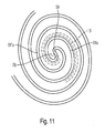
- Fig. 11 is once again the center of the antenna coupler Fig. 7 shown enlarged.
- the strip conductor 15 is shown in broken lines between the two slotted arms 61a, 61'a, which is arranged on the other side of the printed circuit board 8. This crosses in the region of the feed point 59 formed on the first side of the circuit board slot structure. At its end it is connected via a through-hole 76 with the mass metallization 7 formed between the slot structure.
- the small distance between the flat reflector 6 "and the printed circuit board 8 not only leads to a smaller total volume of the antenna coupler but also offers advantages in terms of production.
- the invention is not limited to the illustrated embodiment.
- individual features of different embodiments can be combined with each other in an advantageous manner.
- the frusto-conical reflector 6 can be combined with all spiral-shaped slot structures. It is also possible to use single-arm or multi-arm spirals instead of the two-armed ones shown.
- the respective ends of the slits may be provided with a fishbone-like structure.
- the antenna coupler is provided in particular for coupling in the near field at a distance of up to one wavelength.
Abstract
Description
Die Erfindung betrifft einen Antennenkoppler zum Testen eines Mobilfunkgeräts.The invention relates to an antenna coupler for testing a mobile device.
Beim Testen von Mobilfunkgeräten war es früher üblich, einen separaten Anschluss an dem Mobilfunkgerät vorzusehen, über den das Mobilfunkgerät mit einem Testgerät verbunden wird. Dies hat allerdings den Nachteil, dass lediglich ein Teil der Hardware des Mobilfunkgeräts beim Test zum Einsatz kommt. So erfolgt die Übertragung der Signale nicht etwa über die Funkschnittstelle, sondern über eine kabelgebundene Verbindung. Um diesen Nachteil zu beheben, sind Antennenkoppler entwickelt worden. Diese Antennenkoppler nutzen eine kapazitive oder induktive Kopplung, um zur Durchführung des Tests Signale zwischen dem Mobilfunkgerät und dem an den Antennenkoppler angeschlossenen Testgerät zu übertragen. Ein Problem dabei ist, dass unterschiedliche Mobilfunkgeräte in unterschiedlichen Frequenzbereichen arbeiten. Dies erfordert in der Regel die Anordnung von mehreren Antennen in dem Koppler, wobei aufgrund des selektiven Verhaltens der Antennen eine genaue Positionierung des Mobilfunkgeräts relativ zu den jeweiligen Antennen erfolgen muss. Um dieses Problem zu lösen, ist es aus der
Es ist daher die Aufgabe der Erfindung, einen Antennenkoppler zu schaffen, welcher breitbandig einsetzbar ist und bei dem der Einfluss von metallischen Objekten im Nahfeld auf das Verhalten möglichst gering ist.It is therefore the object of the invention to provide an antenna coupler which can be used in a broadband manner and in which the influence of metallic objects in the near field on the behavior is as low as possible.
Die Aufgabe wird durch den erfindungsgemäßen Antennenkoppler mit den Merkmalen des Anspruchs 1 gelöst.The object is achieved by the antenna coupler according to the invention with the features of claim 1.
Der erfindungsgemäße Antennenkoppler zum Testen eines Mobilfunkgeräts weist ein mittels Leiterbahnen auf einer Leiterplatte flächig ausgebildetes Kopplungselement auf. Auf einer ersten Seite einer Leiterplatte ist eine Aufnahmevorrichtung zur Positionierung eines Mobilfunkgeräts in unmittelbarer Nähe des Kopplungselements ausgebildet. Auf der ersten Seite der Leiterplatte ist zumindest eine Schlitzstruktur in eine dort ausgebildete Massemetallisierung eingebracht. Zur Speisung der als Koppelelement dienenden Schlitzstruktur dient ein auf der zweiten, von der Massemetallisierung abgewandten Seite der Leiterplatte ausgebildeter Streifenleiter. Dieser Streifenleiter bildet mit den auf der ersten Seite ausgebildeten verbleibenden Teilen der Massemetallisierung eine Mikrostripleitung aus.The antenna coupler according to the invention for testing a mobile radio device has a coupling element formed by means of strip conductors on a printed circuit board. On a first side of a printed circuit board, a receiving device for positioning a mobile device in the immediate vicinity of the coupling element is formed. On the first side of the printed circuit board at least one slot structure is introduced into a mass metallization formed there. To feed the slot structure serving as coupling element, a strip conductor formed on the second side of the printed circuit board facing away from the mass metallization is used. This strip conductor forms a microstrip line with the remaining parts of the mass metallization formed on the first side.
Durch die Verwendung einer breitbandig wirkenden, auf einer Leiterplatte ausgebildeten Antennenstruktur deren flächig ausgebildetes Kopplungselement als Schlitzstruktur ausgebildet ist, wird erreicht, dass lediglich eine Antenne vorgesehen sein muss, um die üblichen Mobilfunkfrequenzen abzudecken. Der Einfluss, der bei herkömmlichen Antennen, die eine solche breitbandige Anwendung erlauben, aufgrund der metallischen Objekte, beispielsweise innerhalb des Mobilfunkgeräts, vorhanden sind, wird dabei durch die Verwendung einer Schlitzstruktur unterdrückt. Die Verwendung einer solchen Schlitzstruktur ist insbesondere deswegen von Vorteil, da die üblichen Näherungen bei der Betrachtung von Antennen aufgrund der Wechselwirkung im Nahfeldbereich nicht greifen.By using a broadband acting, formed on a printed circuit board antenna structure whose areal coupling element as a slot structure is formed, it is achieved that only one antenna must be provided to cover the usual mobile radio frequencies. The influence that is present in conventional antennas, which allow such a broadband application, due to the metallic objects, for example within the mobile device, is thereby suppressed by the use of a slot structure. The use of such a slot structure is particularly advantageous because the usual approximations in the observation of antennas due to the interaction in the near field range does not apply.
In den Unteransprüchen sind vorteilhafte Weiterbildungen des erfindungsgemäßen Antennenkopplers ausgeführt.In the dependent claims advantageous developments of the antenna coupler according to the invention are carried out.
Insbesondere ist es bevorzugt, die Schlitzstruktur spiralförmig auszubilden. Mit einer solchen spiralförmigen Schlitzstruktur lässt sich innerhalb der in der Regel recht begrenzten geometrischen Abmessung, die der Antennenkoppler aufweisen darf, ein hervorragendes Kopplungsergebnis erzielen. Durch die schlitzartige und spiralenförmig gewundene Kopplungsstruktur wird ein hervorragender Koppelfaktor erreicht, ohne dass die Performance des gesamten Antennenkopplers durch die Wechselwirkung mit den bereits erläuterten metallischen Objekten verschlechtert wird.In particular, it is preferable to form the slot structure in a spiral shape. With such a spiral slot structure, an excellent coupling result can be achieved within the usually quite limited geometric dimension which the antenna coupler is allowed to have. The slit-like and helically wound coupling structure achieves an excellent coupling factor without impairing the performance of the entire antenna coupler through the interaction with the metallic objects already explained.
Als besonders geeignet hat sich dabei herausgestellt, wenn ausgehend von einem den Mittelpunkt der Spirale bildenden Speisepunkt der zumindest einarmigen spiralförmigen Schlitzantenne eine archimedische Spirale ausgebildet ist, die in einem weiter von dem Speisepunkt entfernten Bereich in eine logarithmische Spirale übergeht. Eine solche Anordnung hat sich als besonders geeignet zum Ausbilden einer breitbandig wirkenden Kopplungseinrichtung für Mobilfunkgeräte herausgestellt.It has proven to be particularly suitable if, starting from a center point of the spiral forming feed point of the at least one arm spiral slot antenna, an Archimedean spiral is formed, which merges into a logarithmic spiral in an area further away from the feed point. Such Arrangement has been found to be particularly suitable for forming a broadband acting coupling device for mobile devices.
Das von dem Speisepunkt entfernte Ende eines jeden Schlitzarms bei spiralförmiger Struktur ist vorzugsweise durch eine Mehrzahl von aufeinander folgend angeordneten Widerständen abgeschlossen. Diese sind, vorzugsweise in SMD-Technik, so angeordnet, dass sie den Schlitz der Schlitzstruktur überspannen. Damit lässt sich ein impedanzrichtiger Abschluss der jeweiligen Schlitzstrukturen erreichen, wobei der erforderliche Platzbedarf sehr gering ist.The end of each slit arm of helical structure remote from the feed point is preferably terminated by a plurality of successively arranged resistors. These are arranged, preferably in SMD technology, so that they span the slot of the slot structure. This makes it possible to achieve an impedance-compliant termination of the respective slot structures, the space required being very small.
Alternativ zu der spiralförmigen Ausbildung kann auch eine sogenannte logarithmisch-periodische Schlitzantenne als Kopplungselement ausgebildet sein. Dabei wird eine Mehrzahl von parallel angeordneten geraden Schlitzelementen auf der ersten Seite der Leiterplatte durch Unterbrechen der dort ausgebildeten Massemetallisierungen ausgebildet, deren Länge mit zunehmendem Abstand von einem Speisepunkt zunimmt. Die einzelnen Schlitzelemente sind an einem Ende mit einander verbunden, wobei das so ausgebildete gemeinsame Schlitzteil senkrecht auf der Erstreckungsrichtung der Schlitzelemente steht. Eine solche Anordnung hat den Vorteil, dass ein zur Verbesserung der Eigenschaften der Kopplungsstruktur verwendeter Reflektor besonders einfach geformt werden kann.As an alternative to the spiral-shaped configuration, a so-called logarithmic periodic slot antenna can also be designed as a coupling element. In this case, a plurality of parallel arranged straight slot elements on the first side of the circuit board is formed by interrupting the mass metalizations formed there, the length of which increases with increasing distance from a feed point. The individual slot elements are connected at one end to each other, wherein the thus formed common slot part is perpendicular to the extension direction of the slot elements. Such an arrangement has the advantage that a reflector used to improve the properties of the coupling structure can be shaped particularly easily.
Die Schlitzbreite der Schlitzarme im Falle einer spiralförmigen Schlitzstruktur beziehungsweise die Schlitzbreite der Schlitzelemente und eines gemeinsamen Schlitzteils im Falle einer logarithmisch-periodischen Schlitzstruktur nimmt gemäß einer bevorzugten Ausführungsform mit zunehmendem Abstand von dem Speisepunkt zu. Gemäß einer anderen Ausführungsform, ist es bei spiralförmigen Schlitzstrukturen insbesondere vorteilhaft, über den gesamten Frequenzbereich, in dem die Antennenstruktur als Koppelelement eingesetzt wird, eine gleichmäßige Schlitzbreite vorzusehen.The slot width of the slot arms in the case of a spiral slot structure or the slot width of the slot elements and a common slot portion in the case of a logarithmic-periodic Slot structure increases according to a preferred embodiment with increasing distance from the feed point. According to another embodiment, in the case of spiral slot structures, it is particularly advantageous to provide a uniform slot width over the entire frequency range in which the antenna structure is used as the coupling element.
Die Koppelungseigenschaften können weiter verbessert werden, wenn die Schlitzstrukturen mäanderförmig ausgebildet sind. Die mäanderförmige Geometrie kann dabei z. B. eine Rechteckstruktur, eine Dreiecksstruktur oder einen sinusförmigen Verlauf aufweisen. Während die Gesamtgeometrie spiralförmig oder aber logarithmischperiodisch ist, folgen die einzelnen Schlitzarme beziehungsweise Schlitzelemente dieser Grundform mäanderförmig.The coupling properties can be further improved if the slot structures are formed meander-shaped. The meandering geometry can be z. B. have a rectangular structure, a triangular structure or a sinusoidal shape. While the overall geometry is spiral-shaped or logarithmic periodic, the individual slit arms or slit elements of this basic shape follow meandering.
Auf der zweiten Seite der Leiterplatte ist vorzugsweise ein Reflektor ausgebildet. Im Falle einer spiralförmigen Schlitzstruktur ist dieser kegelstumpfförmig ausgebildet, im Falle einer logarithmisch-periodischen Koppelelementgeometrie dagegen als Prisma. Besonders bevorzugt ist es dabei, wenn der Reflektor durch einen Gehäuseteil des Antennenkopplers ausgebildet wird. Das Gehäuse ist dabei vorzugsweise als kastenförmig geschlossenes Gehäuse ausgebildet, wobei ein Deckelelement aufklappbar ausgeführt ist. Das Unterteil dient dabei der Aufnahme der Leiterplatte des Antennenkopplers, wobei der Boden des Unterteils dann vorzugsweise als Reflektor ausgeformt ist. Der Zwischenraum zwischen dem Reflektor und der Schlitzstruktur als Koppelelement kann zum Erzielen besonders guter Messwerte mit einem dielektrischen Material gefüllt werden. Dieses dielektrische Material kann dabei besonders bevorzugt so ausgebildet sein, dass es der Fixierung der Leiterplatte mitsamt den dort ausgebildeten Strukturen dient.On the second side of the circuit board, a reflector is preferably formed. In the case of a spiral-shaped slot structure, this is frusto-conical in the case of a logarithmic-periodic coupling element geometry, however, as a prism. It is particularly preferred in this case if the reflector is formed by a housing part of the antenna coupler. The housing is preferably designed as a box-shaped closed housing, wherein a cover element is designed to be hinged. The lower part serves to receive the printed circuit board of the antenna coupler, wherein the bottom of the lower part is then preferably formed as a reflector. The gap between the reflector and the slot structure as a coupling element can be filled with a dielectric material to achieve particularly good measured values. This Dielectric material may be particularly preferably formed so that it serves to fix the circuit board together with the structures formed there.
Gerne ist es bevorzugt, den Antennenkoppler mit einem ebenen Reflektor auszubilden. Dieser ebene Reflektor ist dann auf der zweiten Seite der Leiterplatte angeordnet. Auf der der Leiterplatte zugewandten Seite des Reflektors ist ein Absorbermaterial angeordnet. Aufgrund der ebenen Anordnung kann der gesamte Bauraum des Antennenkopplers verringert werden. Dabei ist für Anwendungen im Mobilfunkbereich vorzugsweise ein Abstand zwischen der Leiterplatte und dem Reflektor von etwa 16 mm vorgesehen.It is preferred to form the antenna coupler with a planar reflector. This planar reflector is then arranged on the second side of the circuit board. On the circuit board facing side of the reflector, an absorber material is arranged. Due to the planar arrangement of the entire installation space of the antenna coupler can be reduced. In this case, a distance between the circuit board and the reflector of about 16 mm is preferably provided for applications in the mobile sector.
Besonders vorteilhaft ist es, ein Absorbermaterial auf dem Reflektor vorzusehen, dessen Dicke maximal ein Drittel des Abstands zwischen dem Reflektor und der Leiterplatte beträgt. Besonders bevorzugt wird eine Dicke des Absorbermaterials von 5 mm bei einem Abstand zwischen Reflektor und Leiterplatte von 16 mm vorgesehen. Das Absorbermaterial ist dabei insbesondere ein kohlegefüllter Absorberschaum. Diese Anordnung hat den Vorteil, dass eine geringe Welligkeit durch die gedämpften Reflexionen auftritt.It is particularly advantageous to provide an absorber material on the reflector whose thickness is at most one third of the distance between the reflector and the printed circuit board. Particularly preferred is a thickness of the absorber material of 5 mm provided at a distance between the reflector and the circuit board of 16 mm. The absorber material is in particular a carbon-filled absorber foam. This arrangement has the advantage that a small ripple occurs due to the damped reflections.
In der Zeichnung sind Beispiele des erfindungsgemäßen Antennenkopplers dargestellt, die in der nachfolgenden Beschreibung näher erläutert werden. Es zeigen:
-
Fig. 1 eine perspektivische Darstellung eines geöffneten Gehäuses eines erfindungsgemäßen Antennenkopplers; -
Fig. 2a einen Antennenkoppler mit einer spiralförmigen Schlitzgeometrie und einem Reflektor; -
Fig. 2b einen kegelstumpfförmigen Reflektor für spiralförmige Schlitzstrukturen; -
Fig. 3a eine logarithmisch-periodische Struktur als Koppelelement mit einem entsprechend ausgebildeten Reflektor; -
Fig. 3b eine dreidimensionale Darstellung eines Reflektors für eine logarithmisch-periodische Schlitzstruktur; -
Fig. 4 eine zweiarmige archimedische Spirale als Schlitzstruktur; -
Fig. 5 ein weiteres Beispiel für eine zweiarmige archimedische Spirale; -
Fig. 6 eine zweiarmige logarithmische Spirale mit breiter werdenden Schlitzarmen; -
Fig. 7 eine im Innenbereich archimedische und im äußeren Bereich logarithmische zweiarmige Spirale mit konstanter Schlitzarmbreite; -
Fig. 8 ein Beispiel zur Erläuterung von mäanderförmigen Schlitzgeometrieen; -
Fig. 9 einen Teilschnitt durch einen in dem Gehäuse derFig. 1 angeordneten Antennenkoppler; -
Fig. 10 einen Teilschnitt durch einen in dem Gehäuse derFig. 1 angeordneten Antennenkoppler mit einem ebenen Reflektor; und -
Fig. 11 eine detaillierte Darstellung des Zentrums der logarithmischen zweiarmigen Spirale derFig. 7 zur Verdeutlichung des Erregerzentrums.
-
Fig. 1 a perspective view of an open housing of an antenna coupler according to the invention; -
Fig. 2a an antenna coupler having a spiral slot geometry and a reflector; -
Fig. 2b a frusto-conical reflector for spiral slot structures; -
Fig. 3a a logarithmic-periodic structure as a coupling element with a correspondingly formed reflector; -
Fig. 3b a three-dimensional representation of a reflector for a logarithmic-periodic slot structure; -
Fig. 4 a two-armed Archimedean spiral as a slot structure; -
Fig. 5 another example of a two-armed Archimedean spiral; -
Fig. 6 a two-armed logarithmic spiral with widening slit arms; -
Fig. 7 an Archimedean in the interior and logarithmic in the outer area two-armed spiral with constant Schlitzarmbreite; -
Fig. 8 an example for explaining meandering slot geometries; -
Fig. 9 a partial section through one in the housing ofFig. 1 arranged antenna coupler; -
Fig. 10 a partial section through one in the housing ofFig. 1 arranged antenna coupler with a planar reflector; and -
Fig. 11 a detailed representation of the center of the logarithmic two - armed spiral ofFig. 7 to clarify the pathogen center.
Die
Ebenso ist ein zweites Volumen in dem Deckelteil 2b ausgebildet. Dieses zweite Volumen 5 ist in der dargestellten Ausführung des Gehäuses 1 leer. Es ist jedoch ebenso gut denkbar, dass das zweite Volumen 5 mit einem Absorbermaterial gefüllt ist. Beispielsweise können pyramidale Strukturen in einem absorbierenden Material ausgeführt sein, wobei das gesamte Absorberelement am Deckelteil 2b befestigt ist. Ferner ist an dem Deckelteil 2b ein Verschlussmechanismus 3 ausgebildet. Im dargestellten Ausführungsbeispiel ist dieser drehbar und greift in eine Arretiernase am Unterteil 2a ein. Bei geschlossenem Deckelteil 2b bildet das Gehäuse 1 eine hochfrequenzdichte, geschlossene Einheit aus, so dass ein Test eines darin befindlichen Mobilfunkgeräts nicht durch externe Störquellen gestört werden kann.Likewise, a second volume is formed in the
In der
Die Ausbildung der Schlitzstruktur in der Massemetallisierung 7 kann auf herkömmliche Weise, beispielsweise durch Ätzen erfolgen.The formation of the slot structure in the
Auf der von der Massemetallisierung 7 abgewandten zweiten Seite der Leiterplatte 8 ist ein Reflektor 6 angeordnet. Durch den Reflektor 6, einem metallischen Element, überlagern sich die elektromagnetischen Felder auf der dem zu testenden Mobilfunkgerät zugewandten ersten Seite der Leiterplatte 8 positiv.On the side facing away from the
In Abhängigkeit von der Frequenz ergibt sich jeweils eine sogenannte aktive Zone der Schlitzstruktur als Koppelungselement. Die aktive Zone ist im Wesentlichen ein Kreisring, dessen Mittelpunkt mit dem Speisepunkt 9 zusammenfällt. Mit zunehmender Frequenz reduziert sich der mittlere Durchmesser des Kreisrings. Da der Abstand des Reflektors 6 von der zweiten Seite der Leiterplatte 8 von der Wellenlänge abhängt, ergibt sich bei Berücksichtigung einer oberen Grenzfrequenz eine kegelstumpfförmige Geometrie des Reflektors 6. Eine solche kegelstumpfförmige Geometrie ist in der
Da die Schlitzstrukturen auch Leitungseigenschaften besitzen und somit elektromagnetische Wellen durch die Schlitze geführt werden, gibt es einen Koppelmechanismus über Nah-/ und Streufelder. Es kann daher auch eine Kopplung unterhalb einer theoretischen unteren Grenzfrequenz der Struktur auftreten.Since the slot structures also have line properties and thus electromagnetic waves are guided through the slots, there is a coupling mechanism on near and stray fields. It can therefore also occur a coupling below a theoretical lower limit frequency of the structure.
Ein weiteres Beispiel für einen Antennenkoppler 20 und die Ausbildung einer Schlitzstruktur als Kopplungselement samt dem zugehörigen Reflektor zur Verbesserung des Antennengewinns ist in den
Das jeweils von dem gemeinsamen Schlitzteil 23 abgewandte Ende eines Schlitzelements 21.i ist so ausgebildet, dass die Enden der Schlitzelemente 21.i, die sich zu einer Seite des gemeinsamen Schlitzteils 23 erstrecken, auf einer gemeinsamen, durch den Speisepunkt 19 verlaufenden Geraden liegen. Dies gilt für die zur anderen Seite des gemeinsamen Schlitzteils 23 sich erstreckenden Schlitzelement 21.i in gleicher Weise. Die äußere Begrenzung der sich ergebenden gesamten Schlitzstruktur ist daher näherungsweise gleich einem Schnitt durch einen Doppelkegel. Die aktive Zone wird jeweils durch diejenigen Schlitzelemente 21.i gebildet, deren Länge ca. λ/4 oder etwas kürzer ist.The respectively remote from the
Aufgrund der sich ergebenden Symmetrie ist der Reflektor 6' nun nicht mehr als Kegelstumpf ausgebildet, sondern als gerades Prisma, mit einem gleichschenkligen Trapez als Grundfläche. Auf diese Weise ergibt sich wiederum ein Reflektorsegment 25, welches in Abhängigkeit der oberen Grenzfrequenz mit einem bestimmten Abstand von der zweiten Seite der Leiterplatte 8, auf der die logarithmisch-periodische Schlitzstruktur ausgebildet ist, angeordnet ist. Beidseits davon ist eine erste Reflektorfläche 24 bzw. eine zweite Reflektorfläche 24' ausgebildet, deren Abstand von der zweiten Seite der Leiterplatte 8 mit zunehmender Entfernung von dem Reflektorsegment 25 zunimmt.Due to the resulting symmetry of the reflector 6 'is now no longer designed as a truncated cone, but as a straight prism, with an isosceles trapezium as a base. In this way, in turn results in a
Besonders bevorzugt ist es, wenn der Reflektor 6 beziehungsweise 6' durch den Boden des Unterteils 2a des Gehäuses 1 ausgebildet ist. Ein zusätzliches Bauteil kann somit entfallen.It is particularly preferred if the
In der
In der
Ein weiteres Ausführungsbeispiel für eine Schlitzstruktur ist in der
Anstelle der zunächst äquidistanten Schlitzarmteile des jeweils ersten Bereichs 61a, 61'a weitet sich die Spirale mit zweiten Schlitzarmteilen in den zweiten Bereichen 61b beziehungsweise 61'b des ersten Schlitzarms 61 beziehungsweise des zweiten Schlitzarms 61' auf.Instead of the first equidistant slot arm portions of the respective
Wie schon bei der logarithmischen Spirale der
Die vorangegangenen Beispiele zeigen jeweils Schlitzelemente beziehungsweise Schlitzarme, bei denen die Ausbildung des Rands der den Schlitz bildenden Massemetallisierung im Wesentlichen geradlinig, beziehungsweise entsprechend dem Verlauf der Spirale gekrümmt verläuft. In der
Die mäanderförmige Struktur 70 wird insbesondere im Auslauf der Schlitzarme vorgesehen. So kann, wie es in den
Die
In der
In der
In der
Der geringe Abstand zwischen dem ebenen Reflektor 6" und der Leiterplatte 8 führt nicht nur zu einem kleineren gesamten Bauvolumen des Antennenkopplers sondern bietet überdies auch noch Vorteile in der Fertigung. Der Zerspanungsaufwand für das Gehäuse des Antennenkopplers ist damit erheblich reduziert.The small distance between the
Die Erfindung ist nicht auf das dargestellte Ausführungsbeispiel beschränkt. Insbesondere sind auch einzelne Merkmale verschiedener Ausführungsbeispiele in vorteilhafter Weise miteinander kombinierbar. So ist insbesondere der kegelstumpfförmige Reflektor 6 mit sämtlichen spiralförmigen Schlitzstrukturen kombinierbar. Es können außerdem auch ein- oder mehrarmige Spiralen anstelle der gezeigten zweiarmigen eingesetzt werden.The invention is not limited to the illustrated embodiment. In particular, individual features of different embodiments can be combined with each other in an advantageous manner. Thus, in particular, the frusto-
Zur Verbesserung des Abschlusses der Schlitzelemente bzw. Schlitzarme können die jeweiligen Enden der Schlitze außerdem mit einer fischgrätähnlichen Struktur versehen sein. Der Antennenkoppler ist insbesondere zur Kopplung im Nahfeld mit einem Abstand von bis zu einer Wellenlänge vorgesehen.In addition, in order to improve the termination of the slit members, the respective ends of the slits may be provided with a fishbone-like structure. The antenna coupler is provided in particular for coupling in the near field at a distance of up to one wavelength.
Claims (15)
dadurch gekennzeichnet,
dass auf der ersten Seite der Leiterplatte (8) zumindest eine Schlitzstruktur (11, 11', 21.i, 23, 31, 31', 41, 41', 51, 51', 61, 61') in eine dort ausgebildete Massemetallisierung (7) eingebracht ist und zur Speisung der als Koppelelement dienenden Schlitzstruktur (11, 11', 21.i, 23, 31, 31', 41, 41', 51, 51', 61, 61') zumindest ein auf der davon abgewandten zweiten Seite ausgebildeter Streifenleiter (15) mit der zwischen der Schlitzstruktur (11, 11', 21.i, 23, 31, 31', 41, 41', 51, 51', 61, 61') der ersten Seite verbleibenden Massemetallisierung (7) eine Mikrostripleitung ausbildet.Antenna coupler for testing a mobile device with a coupling element formed on a printed circuit board by a printed circuit board (8) and having a receiving device (18) for positioning a mobile device in the vicinity of the coupling element, on a first side of the printed circuit board (8),
characterized,
in that at least one slot structure (11, 11 ', 21.i, 23, 31, 31', 41, 41 ', 51, 51', 61, 61 ') is formed on the first side of the printed circuit board (8) in a mass metallization formed there (7) is introduced and for feeding the serving as a coupling element slot structure (11, 11 ', 21.i, 23, 31, 31', 41, 41 ', 51, 51', 61, 61 ') at least one on the thereof remote second side formed stripline (15) with the remaining between the slot structure (11, 11 ', 21.i, 23, 31, 31', 41, 41 ', 51, 51', 61, 61 ') of the first side mass metallization (7) forms a microstrip line.
dadurch gekennzeichnet,
dass die Schlitzstruktur (11, 11', 31, 31', 41, 41', 51, 51', 61, 61') spiralförmig ausgebildet ist.Antenna coupler according to claim 1,
characterized,
in that the slot structure (11, 11 ', 31, 31', 41, 41 ', 51, 51', 61, 61 ') is helical.
dadurch gekennzeichnet,
dass die spiralförmige Schlitzstruktur (11, 11', 31, 31', 41, 41', 51, 51', 61, 61') im Bereich um einen Speisepunkt herum zunächst durch zumindest einen Schlitzarmteil (61a, 61'a) ausgebildet ist, der eine archimedische Spirale beschreibt, wobei der zumindest eine Schlitzarmteil (61a, 61'a) in einem von dem Speisepunkt (59) weiter entfernten Bereich in einen zweiten Schlitzarmteil (61b, 61'b) übergeht, der eine logarithmische Spirale beschreibt.Antenna coupler according to claim 2,
characterized,
in that the spiral-shaped slot structure (11, 11 ', 31, 31', 41, 41 ', 51, 51', 61, 61 ') in the region around a feeding point is initially characterized by at least one Slit arm portion (61a, 61'a) is formed, which describes an Archimedean spiral, wherein the at least one Schlitzarmteil (61a, 61'a) in a farther from the feed point (59) region in a second Schlitzarmteil (61b, 61'b ), which describes a logarithmic spiral.
dadurch gekennzeichnet,
dass ein jeweils von dem Speisepunkt (9, 29, 39, 49, 59) abgewandtes Ende (12, 12', 32, 32', 42, 42', 52, 52', 62, 62') eines Schlitzarms (11, 11', 21.i, 23, 31, 31', 41, 41', 51, 51', 61, 61') mittels mehrerer in Schlitzrichtung aufeinanderfolgend angeordneter Widerstände (33, 33', 43, 43', 53, 53', 63, 63') abgeschlossen ist.Antenna coupler according to claim 2 or 3,
characterized,
in that a respective end (12, 12 ', 32, 32', 42, 42 ', 52, 52', 62, 62 ') facing away from the feed point (9, 29, 39, 49, 59) of a slotted arm (11, 11 ', 21.i, 23, 31, 31', 41, 41 ', 51, 51', 61, 61 ') by means of a plurality of successively arranged in the slot direction resistances (33, 33', 43, 43 ', 53, 53 ', 63, 63') is completed.
dadurch gekennzeichnet,
dass die Schlitzstruktur durch eine Mehrzahl von parallel angeordneten geraden Schlitzelementen (21.i) besteht, deren Länge mit zunehmendem Abstand von dem Speisepunkt (19) zunimmt.Antenna coupler according to claim 1,
characterized,
in that the slot structure consists of a plurality of parallel straight slot elements (21.i), the length of which increases with increasing distance from the feed point (19).
dadurch gekennzeichnet,
dass die Schlitzelemente (21.i) sich in Bezug auf einen gemeinsamen Schlitzteil (23), der sich senkrecht zur Erstreckungsrichtung der Schlitzelemente (21.i) und bis zu dem Speisepunkt (19) erstreckt, abwechselnd in eine erste und eine entgegengesetzte zweite Richtung erstrecken.Antenna coupler according to claim 7,
characterized,
in that the slot elements (21.i) alternately extend in a first and an opposite second direction with respect to a common slot part (23) extending perpendicular to the extension direction of the slot elements (21.i) and to the feed point (19) extend.
dadurch gekennzeichnet,
dass die Schlitzarme (11, 11', 31, 31', 41, 41', 51, 51', 61, 61') oder die Schlitzelemente (21.i) und/oder der gemeinsame Schlitzteil (23) mit zunehmendem Abstand von dem Speisepunkt (9, 19, 29, 39, 49, 59) eine zunehmende Breite (bri) aufweisen.Antenna coupler according to claim 7 or 8,
characterized,
in that the slot arms (11, 11 ', 31, 31', 41, 41 ', 51, 51', 61, 61 ') or the slot elements (21.i) and / or the common slot part (23) increase with increasing distance from the feeding point (9, 19, 29, 39, 49, 59) have an increasing width (br i ).
dadurch gekennzeichnet,
dass die Schlitzbreite der Schlitzarme (11, 11', 31, 31', 41, 41', 51, 51', 61, 61') konstant ist.Antenna coupler according to one of claims 2 to 4,
characterized,
that the slit width of the slit arms (11, 11 ', 31, 31', 41, 41 ', 51, 51', 61, 61 ') is constant.
dadurch gekennzeichnet,
dass die Schlitzstrukturen zumindest teilweise durch mäanderförmige Schlitzränder begrenzt werden.Antenna coupler according to one of claims 1 to 8,
characterized,
that the slot structures are at least partially bounded by meandering slot edges.
dadurch gekennzeichnet,
dass die erste Seite der Leiterplatte (8) mit einem dielektrischen Material (17) abgedeckt ist und an der von der ersten Seite abgewandten Seite des dielektrischen Materials die Aufnahmevorrichtung (18) ausgebildet ist.Antenna coupler according to one of Claims 1 to 9,
characterized,
that the first side of the circuit board (8) with a dielectric material (17) is covered and the receiving device on the side remote from the first side face of the dielectric material (18) is formed.
dadurch gekennzeichnet,
dass auf der zweiten Seite der Leiterplatte (8) ein Reflektor (6, 6') ausgebildet ist, der im Falle einer spiralförmigen Schlitzstruktur kegelstumpfförmig und im Falle von als parallele Schlitzelemente (21.i) ausgebildeter Schlitzstruktur als Prisma ausgebildet ist.Antenna coupler according to one of claims 1 to 10,
characterized,
in that on the second side of the printed circuit board (8) a reflector (6, 6 ') is formed, which in the case of a spiral-shaped slot structure is frustoconical and in the case of parallel slit elements (21.i) trained slot structure is designed as a prism.
dadurch gekennzeichnet,
dass der Reflektor (6, 6') durch ein Gehäuseteil (2a) des Antennenkopplers gebildet wird.Antenna coupler according to claim 11,
characterized,
that the reflector (6, 6 ') by a housing part (2a) of the antenna coupler is formed.
dadurch gekennzeichnet,
dass ein Zwischenraum zischen dem Reflektor (6, 6') und der Schlitzstruktur mit einem dielektrischen Material (16) gefüllt ist.Antenna coupler according to one of claims 11 or 12,
characterized,
is filled that a gap in between the reflector (6, 6 ') and the slot structure with a dielectric material (16).
dadurch gekennzeichnet,
dass auf der zweiten Seite der Leiterplatte (8) ein ebener Reflektor (6") ausgebildet ist, auf dessen der Leiterplatte (8) zugewandten Seite ein Absorbermaterial angeordnet ist.Antenna coupler according to one of claims 1 to 10,
characterized,
that is formed on the second side of the printed circuit board (8), a flat reflector (6 "), on which the circuit board (8) side facing an absorber material is arranged.
dadurch gekennzeichnet,
dass die Dicke des Absorbermaterials bis maximal 1/3 des Abstands des Reflektors 6" von der Leiterplatte (8) beträgt.Antenna coupler according to claim 14,
characterized,
that the thickness of the absorber material is up to 1/3 of the distance between the reflector 6 "from the circuit board (8).
Priority Applications (5)
| Application Number | Priority Date | Filing Date | Title |
|---|---|---|---|
| EP09005697A EP2081254B1 (en) | 2007-12-18 | 2008-04-25 | Antenna coupler |
| EP08008065A EP2073312B1 (en) | 2007-12-18 | 2008-04-25 | Antenna coupler |
| JP2010538451A JP5357178B2 (en) | 2007-12-18 | 2008-12-17 | Antenna coupler |
| PCT/EP2008/010757 WO2009077171A1 (en) | 2007-12-18 | 2008-12-17 | Antenna coupler |
| US12/809,250 US8810461B2 (en) | 2007-12-18 | 2008-12-17 | Antenna coupler |
Applications Claiming Priority (2)
| Application Number | Priority Date | Filing Date | Title |
|---|---|---|---|
| EP07024557 | 2007-12-18 | ||
| EP08008065A EP2073312B1 (en) | 2007-12-18 | 2008-04-25 | Antenna coupler |
Related Child Applications (2)
| Application Number | Title | Priority Date | Filing Date |
|---|---|---|---|
| EP09005697A Division EP2081254B1 (en) | 2007-12-18 | 2008-04-25 | Antenna coupler |
| EP09005697.9 Division-Into | 2009-04-23 |
Publications (2)
| Publication Number | Publication Date |
|---|---|
| EP2073312A1 true EP2073312A1 (en) | 2009-06-24 |
| EP2073312B1 EP2073312B1 (en) | 2011-04-20 |
Family
ID=39739670
Family Applications (2)
| Application Number | Title | Priority Date | Filing Date |
|---|---|---|---|
| EP09005697A Active EP2081254B1 (en) | 2007-12-18 | 2008-04-25 | Antenna coupler |
| EP08008065A Active EP2073312B1 (en) | 2007-12-18 | 2008-04-25 | Antenna coupler |
Family Applications Before (1)
| Application Number | Title | Priority Date | Filing Date |
|---|---|---|---|
| EP09005697A Active EP2081254B1 (en) | 2007-12-18 | 2008-04-25 | Antenna coupler |
Country Status (6)
| Country | Link |
|---|---|
| US (1) | US8810461B2 (en) |
| EP (2) | EP2081254B1 (en) |
| JP (1) | JP5357178B2 (en) |
| AT (1) | ATE513327T1 (en) |
| DE (1) | DE502008003262D1 (en) |
| WO (1) | WO2009077171A1 (en) |
Cited By (1)
| Publication number | Priority date | Publication date | Assignee | Title |
|---|---|---|---|---|
| EP2557631A1 (en) * | 2011-08-08 | 2013-02-13 | Raytheon Company | Continuous current rod antenna |
Families Citing this family (8)
| Publication number | Priority date | Publication date | Assignee | Title |
|---|---|---|---|---|
| FR2965669B1 (en) * | 2010-10-01 | 2012-10-05 | Thales Sa | BROADBAND ANTENNA REFLECTOR FOR CIRCULAR POLARIZED PLANE WIRE ANTENNA AND METHOD FOR PRODUCING THE ANTENNA DEFLECTOR |
| US9437932B1 (en) * | 2011-09-09 | 2016-09-06 | The United States Of America As Represented By The Secretary Of The Navy | Two-arm delta mode spiral antenna |
| WO2013096867A1 (en) * | 2011-12-23 | 2013-06-27 | Trustees Of Tufts College | System method and apparatus including hybrid spiral antenna |
| US9128118B2 (en) | 2012-08-21 | 2015-09-08 | Apple Inc. | Testing systems with automated loading equipment and positioners |
| US20140266149A1 (en) * | 2013-03-12 | 2014-09-18 | Motorola Mobility Llc | Cover-testing fixture for radio frequency sensitive devices |
| KR101471931B1 (en) * | 2013-05-14 | 2014-12-24 | 광주과학기술원 | Antenna apparatus and implementing the same |
| CN110544821A (en) * | 2018-05-28 | 2019-12-06 | 云南电网有限责任公司保山供电局 | Transmission line corona discharge detecting system |
| US11588225B2 (en) * | 2020-10-14 | 2023-02-21 | Bae Systems Information And Electronic Systems Integration Inc. | Low profile antenna |
Citations (11)
| Publication number | Priority date | Publication date | Assignee | Title |
|---|---|---|---|---|
| GB1148320A (en) * | 1965-05-21 | 1969-04-10 | Telefunken Patent | Improvements in or relating to logarithmic aerial systems |
| US4652889A (en) * | 1983-12-13 | 1987-03-24 | Thomson-Csf | Plane periodic antenna |
| US5227807A (en) * | 1989-11-29 | 1993-07-13 | Ael Defense Corp. | Dual polarized ambidextrous multiple deformed aperture spiral antennas |
| US5274390A (en) * | 1991-12-06 | 1993-12-28 | The Pennsylvania Research Corporation | Frequency-Independent phased-array antenna |
| JPH0856112A (en) * | 1994-08-12 | 1996-02-27 | Meisei Electric Co Ltd | Isometric spiral antenna |
| GB2324657A (en) * | 1997-04-26 | 1998-10-28 | Rohde & Schwarz | Aerial coupler for mobile telephones |
| DE19732639C1 (en) * | 1997-07-29 | 1999-01-28 | Wavetek Gmbh | Antenna coupler for testing mobile phones |
| WO2002029928A2 (en) * | 2000-10-02 | 2002-04-11 | Israel Aircraft Industries Ltd. | Slot spiral miniaturized antenna |
| DE102004033383A1 (en) | 2004-04-28 | 2005-11-24 | Willtek Communications Gmbh | antenna |
| EP1619748A1 (en) * | 2001-08-30 | 2006-01-25 | Anritsu Corporation | Portable testing device using an antenna. |
| US7142821B1 (en) * | 2002-12-19 | 2006-11-28 | Itt Manufacturing Enterprises, Inc. | Radio frequency transmitting and receiving module and array of such modules |
Family Cites Families (3)
| Publication number | Priority date | Publication date | Assignee | Title |
|---|---|---|---|---|
| US5053786A (en) * | 1982-01-28 | 1991-10-01 | General Instrument Corporation | Broadband directional antenna |
| US5815122A (en) * | 1996-01-11 | 1998-09-29 | The Regents Of The University Of Michigan | Slot spiral antenna with integrated balun and feed |
| JPH11163622A (en) * | 1997-11-28 | 1999-06-18 | Mitsubishi Electric Corp | Spiral antenna |
-
2008
- 2008-04-25 AT AT09005697T patent/ATE513327T1/en active
- 2008-04-25 DE DE502008003262T patent/DE502008003262D1/en active Active
- 2008-04-25 EP EP09005697A patent/EP2081254B1/en active Active
- 2008-04-25 EP EP08008065A patent/EP2073312B1/en active Active
- 2008-12-17 WO PCT/EP2008/010757 patent/WO2009077171A1/en active Application Filing
- 2008-12-17 JP JP2010538451A patent/JP5357178B2/en not_active Expired - Fee Related
- 2008-12-17 US US12/809,250 patent/US8810461B2/en active Active
Patent Citations (11)
| Publication number | Priority date | Publication date | Assignee | Title |
|---|---|---|---|---|
| GB1148320A (en) * | 1965-05-21 | 1969-04-10 | Telefunken Patent | Improvements in or relating to logarithmic aerial systems |
| US4652889A (en) * | 1983-12-13 | 1987-03-24 | Thomson-Csf | Plane periodic antenna |
| US5227807A (en) * | 1989-11-29 | 1993-07-13 | Ael Defense Corp. | Dual polarized ambidextrous multiple deformed aperture spiral antennas |
| US5274390A (en) * | 1991-12-06 | 1993-12-28 | The Pennsylvania Research Corporation | Frequency-Independent phased-array antenna |
| JPH0856112A (en) * | 1994-08-12 | 1996-02-27 | Meisei Electric Co Ltd | Isometric spiral antenna |
| GB2324657A (en) * | 1997-04-26 | 1998-10-28 | Rohde & Schwarz | Aerial coupler for mobile telephones |
| DE19732639C1 (en) * | 1997-07-29 | 1999-01-28 | Wavetek Gmbh | Antenna coupler for testing mobile phones |
| WO2002029928A2 (en) * | 2000-10-02 | 2002-04-11 | Israel Aircraft Industries Ltd. | Slot spiral miniaturized antenna |
| EP1619748A1 (en) * | 2001-08-30 | 2006-01-25 | Anritsu Corporation | Portable testing device using an antenna. |
| US7142821B1 (en) * | 2002-12-19 | 2006-11-28 | Itt Manufacturing Enterprises, Inc. | Radio frequency transmitting and receiving module and array of such modules |
| DE102004033383A1 (en) | 2004-04-28 | 2005-11-24 | Willtek Communications Gmbh | antenna |
Non-Patent Citations (1)
| Title |
|---|
| VOLAKIS J L ET AL: "A Broadband Cavity-Backed Slot Spiral Antenna", IEEE ANTENNAS AND PROPAGATION MAGAZINE, IEEE SERVICE CENTER, PISCATAWAY, NJ, US, vol. 43, no. 6, 1 December 2001 (2001-12-01), pages 15 - 26, XP011091638, ISSN: 1045-9243 * |
Cited By (2)
| Publication number | Priority date | Publication date | Assignee | Title |
|---|---|---|---|---|
| EP2557631A1 (en) * | 2011-08-08 | 2013-02-13 | Raytheon Company | Continuous current rod antenna |
| US8665173B2 (en) | 2011-08-08 | 2014-03-04 | Raytheon Company | Continuous current rod antenna |
Also Published As
| Publication number | Publication date |
|---|---|
| JP5357178B2 (en) | 2013-12-04 |
| US20100271267A1 (en) | 2010-10-28 |
| EP2081254B1 (en) | 2011-06-15 |
| ATE513327T1 (en) | 2011-07-15 |
| EP2081254A1 (en) | 2009-07-22 |
| JP2011507423A (en) | 2011-03-03 |
| US8810461B2 (en) | 2014-08-19 |
| EP2073312B1 (en) | 2011-04-20 |
| WO2009077171A1 (en) | 2009-06-25 |
| DE502008003262D1 (en) | 2011-06-01 |
Similar Documents
| Publication | Publication Date | Title |
|---|---|---|
| EP2081254B1 (en) | Antenna coupler | |
| DE2538614C3 (en) | Dielectric resonator | |
| EP1250723B1 (en) | Antenna for a communications terminal | |
| DE2639813C3 (en) | Spiral antenna | |
| DE102007005928A1 (en) | Transmission line transition | |
| DE602004000083T2 (en) | Food for reflector antenna | |
| DE10147921A1 (en) | Planar inverted-F antenna for mobile radio communications has tapered surface element providing electrical connection between resonance body and supply point | |
| DE2930932A1 (en) | RILLED HORN SPOTLIGHT | |
| EP2506363B1 (en) | Waveguide coupling | |
| EP2105991B1 (en) | Dielectric horn antenna | |
| DE19945176B4 (en) | Arrangement of spring contacts in a predetermined grid | |
| DE102004045006B4 (en) | High frequency filter | |
| DE102013201685B4 (en) | Conductor arrangement with dielectric sheath wave barrier | |
| DE2441638A1 (en) | BROADBAND ANTENNA | |
| DE102004033383A1 (en) | antenna | |
| DE102012000762A1 (en) | antenna cover | |
| DE102012022411A1 (en) | High frequency filter with frequency stabilization | |
| DE19843929A1 (en) | Flat antenna with coaxial feed | |
| EP0122391B1 (en) | Broadband microwave radiator | |
| DE102006054459B4 (en) | Broadband antenna | |
| DE102017126112A1 (en) | Input and output device between a circuit carrier and a waveguide | |
| EP1139491A2 (en) | Radiating coaxial high-frequency cable | |
| DE102016117424A1 (en) | Antenna device and method for radiating electromagnetic waves with the antenna device | |
| DE4322044A1 (en) | Dipole probe | |
| DE102014103980A1 (en) | Millimeter wave band radio wave half mirror and method of smoothing the transmission thereof |
Legal Events
| Date | Code | Title | Description |
|---|---|---|---|
| PUAI | Public reference made under article 153(3) epc to a published international application that has entered the european phase |
Free format text: ORIGINAL CODE: 0009012 |
|
| AK | Designated contracting states |
Kind code of ref document: A1 Designated state(s): AT BE BG CH CY CZ DE DK EE ES FI FR GB GR HR HU IE IS IT LI LT LU LV MC MT NL NO PL PT RO SE SI SK TR |
|
| AX | Request for extension of the european patent |
Extension state: AL BA MK RS |
|
| 17P | Request for examination filed |
Effective date: 20090618 |
|
| 17Q | First examination report despatched |
Effective date: 20090727 |
|
| AKX | Designation fees paid |
Designated state(s): DE FR GB |
|
| GRAP | Despatch of communication of intention to grant a patent |
Free format text: ORIGINAL CODE: EPIDOSNIGR1 |
|
| GRAS | Grant fee paid |
Free format text: ORIGINAL CODE: EPIDOSNIGR3 |
|
| GRAA | (expected) grant |
Free format text: ORIGINAL CODE: 0009210 |
|
| AK | Designated contracting states |
Kind code of ref document: B1 Designated state(s): DE FR GB |
|
| REG | Reference to a national code |
Ref country code: GB Ref legal event code: FG4D Free format text: NOT ENGLISH |
|
| REF | Corresponds to: |
Ref document number: 502008003262 Country of ref document: DE Date of ref document: 20110601 Kind code of ref document: P |
|
| REG | Reference to a national code |
Ref country code: DE Ref legal event code: R096 Ref document number: 502008003262 Country of ref document: DE Effective date: 20110601 |
|
| PLBE | No opposition filed within time limit |
Free format text: ORIGINAL CODE: 0009261 |
|
| STAA | Information on the status of an ep patent application or granted ep patent |
Free format text: STATUS: NO OPPOSITION FILED WITHIN TIME LIMIT |
|
| 26N | No opposition filed |
Effective date: 20120123 |
|
| REG | Reference to a national code |
Ref country code: DE Ref legal event code: R097 Ref document number: 502008003262 Country of ref document: DE Effective date: 20120123 |
|
| PGFP | Annual fee paid to national office [announced via postgrant information from national office to epo] |
Ref country code: GB Payment date: 20130422 Year of fee payment: 6 |
|
| PGFP | Annual fee paid to national office [announced via postgrant information from national office to epo] |
Ref country code: FR Payment date: 20130523 Year of fee payment: 6 |
|
| GBPC | Gb: european patent ceased through non-payment of renewal fee |
Effective date: 20140425 |
|
| REG | Reference to a national code |
Ref country code: FR Ref legal event code: ST Effective date: 20141231 |
|
| PG25 | Lapsed in a contracting state [announced via postgrant information from national office to epo] |
Ref country code: GB Free format text: LAPSE BECAUSE OF NON-PAYMENT OF DUE FEES Effective date: 20140425 |
|
| PG25 | Lapsed in a contracting state [announced via postgrant information from national office to epo] |
Ref country code: FR Free format text: LAPSE BECAUSE OF NON-PAYMENT OF DUE FEES Effective date: 20140430 |
|
| P01 | Opt-out of the competence of the unified patent court (upc) registered |
Effective date: 20230525 |
|
| PGFP | Annual fee paid to national office [announced via postgrant information from national office to epo] |
Ref country code: DE Payment date: 20230418 Year of fee payment: 16 |