EP2073272B1 - Vibration sensor and method for manufacturing the vibration sensor - Google Patents
Vibration sensor and method for manufacturing the vibration sensor Download PDFInfo
- Publication number
- EP2073272B1 EP2073272B1 EP07791105.5A EP07791105A EP2073272B1 EP 2073272 B1 EP2073272 B1 EP 2073272B1 EP 07791105 A EP07791105 A EP 07791105A EP 2073272 B1 EP2073272 B1 EP 2073272B1
- Authority
- EP
- European Patent Office
- Prior art keywords
- thin film
- etching
- hole
- vibration sensor
- substrate
- Prior art date
- Legal status (The legal status is an assumption and is not a legal conclusion. Google has not performed a legal analysis and makes no representation as to the accuracy of the status listed.)
- Active
Links
Images








Classifications
-
- H—ELECTRICITY
- H10—SEMICONDUCTOR DEVICES; ELECTRIC SOLID-STATE DEVICES NOT OTHERWISE PROVIDED FOR
- H10D—INORGANIC ELECTRIC SEMICONDUCTOR DEVICES
- H10D48/00—Individual devices not covered by groups H10D1/00 - H10D44/00
- H10D48/50—Devices controlled by mechanical forces, e.g. pressure
-
- B—PERFORMING OPERATIONS; TRANSPORTING
- B81—MICROSTRUCTURAL TECHNOLOGY
- B81C—PROCESSES OR APPARATUS SPECIALLY ADAPTED FOR THE MANUFACTURE OR TREATMENT OF MICROSTRUCTURAL DEVICES OR SYSTEMS
- B81C1/00—Manufacture or treatment of devices or systems in or on a substrate
- B81C1/00015—Manufacture or treatment of devices or systems in or on a substrate for manufacturing microsystems
- B81C1/00134—Manufacture or treatment of devices or systems in or on a substrate for manufacturing microsystems comprising flexible or deformable structures
- B81C1/00182—Arrangements of deformable or non-deformable structures, e.g. membrane and cavity for use in a transducer
-
- H—ELECTRICITY
- H04—ELECTRIC COMMUNICATION TECHNIQUE
- H04R—LOUDSPEAKERS, MICROPHONES, GRAMOPHONE PICK-UPS OR LIKE ACOUSTIC ELECTROMECHANICAL TRANSDUCERS; ELECTRIC HEARING AIDS; PUBLIC ADDRESS SYSTEMS
- H04R19/00—Electrostatic transducers
- H04R19/005—Electrostatic transducers using semiconductor materials
-
- H—ELECTRICITY
- H04—ELECTRIC COMMUNICATION TECHNIQUE
- H04R—LOUDSPEAKERS, MICROPHONES, GRAMOPHONE PICK-UPS OR LIKE ACOUSTIC ELECTROMECHANICAL TRANSDUCERS; ELECTRIC HEARING AIDS; PUBLIC ADDRESS SYSTEMS
- H04R19/00—Electrostatic transducers
- H04R19/04—Microphones
-
- H—ELECTRICITY
- H10—SEMICONDUCTOR DEVICES; ELECTRIC SOLID-STATE DEVICES NOT OTHERWISE PROVIDED FOR
- H10P—GENERIC PROCESSES OR APPARATUS FOR THE MANUFACTURE OR TREATMENT OF DEVICES COVERED BY CLASS H10
- H10P50/00—Etching of wafers, substrates or parts of devices
-
- B—PERFORMING OPERATIONS; TRANSPORTING
- B81—MICROSTRUCTURAL TECHNOLOGY
- B81B—MICROSTRUCTURAL DEVICES OR SYSTEMS, e.g. MICROMECHANICAL DEVICES
- B81B2201/00—Specific applications of microelectromechanical systems
- B81B2201/02—Sensors
- B81B2201/0257—Microphones or microspeakers
-
- B—PERFORMING OPERATIONS; TRANSPORTING
- B81—MICROSTRUCTURAL TECHNOLOGY
- B81B—MICROSTRUCTURAL DEVICES OR SYSTEMS, e.g. MICROMECHANICAL DEVICES
- B81B2201/00—Specific applications of microelectromechanical systems
- B81B2201/02—Sensors
- B81B2201/0285—Vibration sensors
-
- B—PERFORMING OPERATIONS; TRANSPORTING
- B81—MICROSTRUCTURAL TECHNOLOGY
- B81B—MICROSTRUCTURAL DEVICES OR SYSTEMS, e.g. MICROMECHANICAL DEVICES
- B81B2203/00—Basic microelectromechanical structures
- B81B2203/01—Suspended structures, i.e. structures allowing a movement
- B81B2203/0127—Diaphragms, i.e. structures separating two media that can control the passage from one medium to another; Membranes, i.e. diaphragms with filtering function
-
- B—PERFORMING OPERATIONS; TRANSPORTING
- B81—MICROSTRUCTURAL TECHNOLOGY
- B81B—MICROSTRUCTURAL DEVICES OR SYSTEMS, e.g. MICROMECHANICAL DEVICES
- B81B2203/00—Basic microelectromechanical structures
- B81B2203/03—Static structures
- B81B2203/0353—Holes
Definitions
- the present invention relates to a vibration sensor and a method for manufacturing the same, in particular, to a vibration sensor including a thin film such as a diaphragm and a method for manufacturing the same.
- the diaphragm made of silicon has a small internal stress and a low density compared to metal such as aluminum and titanium, and thus a vibration sensor of high sensitivity can be obtained and compliance with a semiconductor integrated circuit manufacturing step is also satisfactory.
- the vibration sensor including such a diaphragm includes a capacitor microphone disclosed in Patent Document 1.
- a diaphragm (movable electrode) and a fixed electrode are formed on a front surface of a semiconductor substrate of a monocrystalline silicon (100) plane, and thereafter, an etching mask is formed at the outer peripheral part of a back surface of the relevant semiconductor substrate, and the semiconductor substrate is etched from the back side until reaching the front surface thereby forming a through-hole at a central part of the semiconductor substrate.
- the diaphragm has a periphery fixed to the front surface of the semiconductor substrate and the central part supported in a hollow state above the through-hole, and thus can be vibrated by audio vibration and the like.
- the thickness of the semiconductor substrate is reduced, the ratio of the opening area of the back surface with respect to the opening area of the front surface of the through-hole can be reduced, but the strength of the semiconductor substrate lowers and handling at the time of manufacturing becomes difficult, and thus reducing the thickness of the semiconductor substrate has limits.
- a through-hole is opened in the semiconductor substrate from the back side by vertical etching such as a so-called DRIE (Deep Reactive Ion Etching) and ICP (Inductively Coupled Plasma). Therefore, the film-type sensor can be miniaturized by an amount the through-hole does not spread in the truncated pyramid shape.
- DRIE Deep Reactive Ion Etching
- ICP Inductively Coupled Plasma
- a method for performing crystal anisotropic etching on the semiconductor substrate from the front side (diaphragm side) is also known, but in such a method, an etching hole needs to be opened in the diaphragm, which etching hole sometimes adversely affects vibration characteristics, strength, and the like of the diaphragm.
- An etching method for forming a through-hole in the substrate by performing crystal anisotropic etching on the (100) plane semiconductor substrate from the back side, and reducing the ratio of the opening area of the back surface with respect to the opening area of the front surface includes a method described in Patent Document 3.
- a sacrifice layer is first formed in a rectangular region to be opened on the front surface of the silicon wafer or the semiconductor substrate, and a thin film of silicon nitride is vapor deposited thereon, and thus the opening area of the back surface of the silicon wafer merely needs to be a size the through-hole can reach the sacrifice layer by anisotropic etching.
- Patent Document 3 describes a semiconductor component comprising a substrate, two flexible pressure sensor diaphragms supported by the substrate, and a fixed electrode between the two diaphragms.
- the two diaphragms and the fixed electrode are electrodes of two differential capacitors.
- the substrate has a hole extending from one surface of the substrate to an opposite surface of the substrate. The hole is located underneath the two diaphragms, and the hole at the opposite surfaces of the substrate is preferably larger than the hole at an interior portion of the substrate.
- Patent Document 5 describes that on an upper plane of a silicon substrate, a vibrating electrode plate is formed through an insulating film. On the vibrating electrode plate, a counter electrode plate is arranged through an insulating film, and an acoustic hole penetrates the counter electrode plate. On the vibrating electrode plate and the counter electrode plate, semi-elliptical holes are opened to vertically face each other.
- Non-patent Document 1 describes a silicon condenser microphone with a corrugated diaphragm. The microphone is fabricated on a single wafer by use of silicon anisotropic etching and sacrificial layer etching techniques, so that no bonding techniques are required.
- Non-patent Document 1 QUANBO ZOU ET AL, "Design and Fabrication of Silicon Condenser Microphone Using Corrugated Diaphragm Technique", JOURNAL OF MICROELECTROMECHANICAL SYSTEMS, IEEE SERVICE CENTER, US, vol. 5, no. 3, 1 September 1996, XP011034717, ISSN: 1057-7157, DOI:10.1109/84.536626
- a method for manufacturing a vibration sensor of the present invention includes: forming, at one part of a front surface of a semiconductor substrate of monocrystalline silicon, a sacrifice layer with a material isotropically etched by an etchant for etching the semiconductor substrate; forming a thin film protective film with a material having resistance to the etchant on the sacrifice layer and the front surface of the semiconductor substrate at a periphery of the sacrifice layer; forming a thin film of monocrystalline silicon, polycrystalline silicon, or amorphous silicon on an upper side of the sacrifice layer; opening a backside etching window in a back surface protective film having resistance to the etchant for etching the semiconductor substrate formed on a back surface of the semiconductor substrate; forming a through-hole in the semiconductor substrate by etching the semiconductor substrate anisotropically by using crystal -oriented etching by applying the etchant from the back surface window, then etching the sacrifice layer isotropically by the etchant after the etchant reaches the front surface of the
- the through-hole is formed by performing crystal anisotropic etching on the semiconductor substrate of monocrystalline silicon from both front and back surfaces, and thus the opening area of the through-hole does not become too large compared to the area of the thin film, and the vibration sensor can be miniaturized. Therefore, the number of elements that can be fabricated from one wafer increases, and the cost of the vibration sensor can be lowered.
- the through-hole can be formed from both surfaces through one etching step, and thus the manufacturing steps are simplified.
- the protective layer is formed between the sacrifice layer and the thin film, the thin film is prevented from being damaged by the etchant when forming the through-hole even if the thin film is made of a material that does not have resistance to the etchant of the semiconductor substrate.
- a vibration sensor of high productivity and high sensitivity can be obtained since the thin film is formed by monocrystalline silicon, polycrystalline silicon, or amorphous silicon.
- the method for manufacturing the vibration sensor includes forming a vent hole for communicating the front side and the back side of the thin film between the holders.
- a vent hole of a long length can be formed, and thus an acoustic resistance can be increased and satisfactory acoustic characteristics can be obtained when used in a microphone, and the like.
- an electrostatic pressure at the front and the back of the thin film can be balanced since the front side and the back side of the thin film are communicated with the vent hole.
- the thin film is a square. According to such an embodiment, the opening formed by performing crystal anisotropic etching of the monocrystalline silicon substrate can be effectively used.
- the holder is arranged at four corners of the thin film. According to such a configuration, the sensitivity of the vibration enhances since the thin film can flexibly deform.
- the sacrifice layer is arranged at one part of the forming region of the thin film so that the thin film is bendable. According to such an embodiment, a displacement of the thin film can be increased and a deflection by stress can be reduced.
- the sacrifice layer is arranged at one part of the forming region of the thin film to form a projection on the front surface of the thin film. According to such an embodiment, the deformed thin film is prevented from area contacting and attaching to the electrode, and the like, when the electrode, and the like are arranged on the upper side of the thin film.
- an area of the cross-section parallel to the opening at the interior of the through-hole is larger than the opening area of the front surface of the through-hole. According to such an embodiment, a volume of the through-hole can be increased, and thus acoustic compliance can be increased when the vibration sensor is used in the acoustic sensor.
- the sacrifice layer is made of polycrystalline silicon or amorphous silicon.
- the sacrifice layer can be simultaneously etched when etching the semiconductor substrate of monocrystalline silicon, whereby the steps can be simplified. Since the polycrystalline silicon and the amorphous silicon have high temperature resistance, high temperature process can be used in the post-step, and the compliance with the semiconductor integrated circuit manufacturing step is also satisfactory.
- the semiconductor substrate can be subjected to crystal anisotropic etching from both the front and the back surfaces starting from the crystal anisotropic etching of the semiconductor substrate from the back side, and thus an etching hole does not need to be formed in the thin film, and a risk of lowering the strength of the thin film or changing the characteristics of the thin film is eliminated.
- the manufacturing steps are simplified as the through-hole can be formed from both surfaces in one etching step.
- a vibration sensor manufactured according to the above-mentioned method of the present invention includes: a semiconductor substrate of monocrystalline silicon formed with a through-hole passing from front to back; at least one holder made of a material having resistance to an etchant for forming the through-hole by etching the semiconductor substrate, and arranged on a front surface of the semiconductor substrate; a thin film having corners supported by the holder, and covering an opening on the substrate front surface side of the through-hole; and at least one vent hole for putting the front side in communication with the back side of the thin film; wherein an area of a cross-section parallel to the substrate front surface of the through-hole gradually decreases or increases from the front surface towards a back surface of the semiconductor substrate, and changes from decrease to increase or from increase to decrease at a middle of the front surface and the back surface of the semiconductor substrate, and the at least one vent hole is formed by a thin film protective film.
- the area of the cross-section parallel to the substrate front surface of the through-hole gradually decreases or increases from the front surface towards the back surface of the semiconductor substrate, and changes from decrease to increase or from increase to decrease at a middle of the front surface and the back surface of the semiconductor substrate, and thus the ratio of the opening area of the through-hole at the front surface of the semiconductor substrate and the opening area of the through-hole at the back surface approaches one, and the vibration sensor can be miniaturized. Since the volume of the through-hole can be increased, the acoustic compliance can be increased when using the vibration sensor in the acoustic sensor.
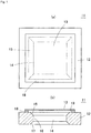
- Fig. 1(a) is a plan view showing a structure of a vibration sensor 11 according to a first embodiment, which does not form part of the present invention
- Fig. 1(b) is a cross-sectional view thereof.
- the vibration sensor 11 is used in an acoustic sensor such as a semiconductor microphone and an ultrasonic sensor, a thin film filter, and the like.
- the vibration sensor 11 includes an Si substrate 12, and a thin film 13 (diaphragm).
- the Si substrate 12 is a (100) plane substrate.
- the Si substrate 12 is etched from the back side so as to form a rectangular through-hole 14, which is passed through from the front to the back and which side in each horizontal and vertical direction lies in the (110) direction.
- the through-hole 14 has inclined surfaces 15, 17 formed on the front side and the back side by a (111) plane or a crystal plane equivalent thereto, and a vertical surface 16 is formed between the inclined surfaces 15, 17.
- the vertical surface 16 is actually configured by a plurality of crystal planes such as a (110) plane, a (311) plane, and a (411) plane, but is shown as a vertical plane for simplification. Therefore, the cross-section of the substrate at the edge of the through-hole 14 has a shape tapered at the front and the back.
- the thin film 13 is arranged on the upper surface of the Si substrate 12 so as to cover the opening on the front side of the through-hole 14, and the entire periphery of the lower surface is fixed to the upper surface of the Si substrate 12 by a holder 18.
- a narrow gap 19 forms between the opening on the front side (or surface that was the front surface of the Si substrate 12) of the through-hole 14 and the back surface of the thin film 13 by the holder 18.
- the vibration sensor 11 of such a structure although the through-hole 14 is formed by etching the Si substrate 12 from the back side, the opening area on the back side does not become too large compared to the opening on the front side of the through-hole 14. Therefore, the area of the Si substrate 12 does not become large by the through-hole 14 as in the first related art.
- the Si substrate 12 merely needs to have a size capable of mounting the thin film 13 and circuit components, as necessary, and the vibration sensor 11 can be miniaturized.
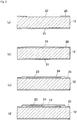
- protective films 20, 21 of SiO 2 are formed on the front surface and the back surface of the (100) plane Si substrate 12 through thermal oxidation method, and the like.
- the protective film 20 at a region to form the gap 19 is then partially removed using a photolithography technique at the front surface of the Si substrate 12, thereby opening a rectangular etching window 22.
- a polycrystalline silicon thin film is formed on the front surface of the Si substrate 12 from above the protective film 20, and the polycrystalline silicon thin film on the protective film 20 is removed using the photolithography technique.
- a rectangular sacrifice layer 23 of polycrystalline silicon thin film thereby forms on the front surface of the Si substrate 12 in the etching window 22. This state is shown in Fig. 2(b) .
- a protective film 24 of SiO 2 is then formed on the front surface of the Si substrate 12 from above the sacrifice layer 23, so that the sacrifice layer 23 is covered by the protective film 24, as shown in Fig. 2(c) .
- a polycrystalline silicon thin film is then formed on the protective film 24, and the unnecessary portion of the polycrystalline silicon thin film is removed using the photolithography technique, so that the thin film 13 of polycrystalline silicon thin film forms on the protective film 24, as shown in Fig. 2(d) . Furthermore, as shown in Fig. 3(a) , a rectangular protective film 25 of SiO 2 is formed on the thin film 13, so that the thin film 13 is covered by the protective film 25.
- part of the protective film 21 is partially removed using the photolithography technique at the back surface of the Si substrate 12, thereby opening a backside etching window 26 to a rectangular shape in the protective film 21.
- the backside etching window 26 merely needs to have a size for crystal anisotropic etching started from the backside etching window 26 to reach the front surface of the Si substrate 12, where a relatively small backside etching window 26 having one side of about 570 ⁇ m is enough for the Si substrate 12 having a thickness of 400 ⁇ m.
- the dimension of the vertical and horizontal size of the sacrifice layer 23 is determined by the dimension of the vertical and horizontal size of the necessary thin film 13, and one side is about 650 ⁇ m, for example.
- etching is performed from the backside etching window 26 by soaking in etchant such as TMAH, KOH, or EDP (hereinafter referred to as etchant such as TMAH).
- etchant such as TMAH
- the etchant such as TMAH performs crystal anisotropic etching on the Si, and thus etching advances along the (111) plane and the crystal plane (inclined surface 17) equivalent thereto at the back surface of the Si substrate 12, thereby forming the through-hole 14 having a truncated pyramid shape at the back surface of the Si substrate 12.
- the sacrifice layer 23 is exposed to the interior of the through-hole 14, as shown in Fig. 3(c) .
- the protective films 20, 21, 24 and 25 of SiO 2 are not etched by the etchant such as TMAH, but the sacrifice layer 23 of polycrystalline silicon is subjected to isotropic etching by the etchant such as TMAH.
- TMAH etchant
- etching proceeds from the portion exposed in the through-hole 14 towards the periphery, thereby forming the gap 19 between the protective film 24 and the front surface of the Si substrate 12, as shown in Fig. 3(d) .
- the thin film 13 and the protective films 24, 25 are lifted from the front surface of the Si substrate 12 by the gap 19, and thus can function as thin films.
- the gap 19 is a space of thin thickness, damping effect occurs when the thin film 13 and the protective films 24, 25 vibrate, which may degrade vibration characteristics of a high frequency band or become a cause of mechanical noise, and the thin film 13 and the protective films 24, 25 tend to easily stick (attach) to the Si substrate 12.
- etching of the Si substrate 12 is further continued at the lower side of the thin film 13.
- the thickness of the gap 19 is designed in view of the above, and is, for example, about 1 ⁇ m.
- the thickness of the thin film 13 is designed in view of the trade-off with the sensitivity and the strength of the vibration sensor 11, and is, for example, about 1 ⁇ m.
- the etchant enters the gap 19, and performs crystal anisotropic etching on the Si substrate 12 from the front side.
- etching advances in the direction shown by the arrow in Fig. 4(a) , thereby forming the inclined surface 15 in the through-hole 14.
- the etching rate is large at the pointed end portion of the edge of the through-hole 14, corners are removed at the inner peripheral surface of the through-hole 14 thereby forming the vertical surface 16, and the through-hole 14 is etched to a shape similar to a doughnut hole.
- the Si substrate 12 is pulled out from the etchant at a point the sacrifice layer 23 is completely etching-removed, as shown in Fig. 4(b) .
- the protective films 20, 21, 24, and 25 of SiO 2 are etched with HF aqueous solution, and the like, where etching is terminated at a point only the holder 18 made from part of the protective films 20, 24 remained, washing and drying are performed, and the vibration sensor 11 is completed, as shown in Fig. 4(c) .
- the through-hole 14 of small spreading can be opened at the back side and the vibration sensor 11 can be miniaturized with only the etching from the back side of the Si substrate 12 by fabricating the vibration sensor 11 in the above manner. Furthermore, since the through-hole 14 can be opened through etching of only from the back side, the etching hole does not need to be opened in the thin film 13, and a risk of changing physical characteristics of the thin film 13 in the vibration sensor 11 or lowering the strength of the thin film 13 is reduced.
- the opening area on the back side of the through-hole 14 is determined by the size of the backside etching window 26 opened in the protective film 21, and the opening area on the front side of the through-hole 14 is determined by the size of the sacrifice layer 23, and thus the opening area of the through-hole 14 can be accurately controlled according to the above-described manufacturing method.
- the sacrifice layer 23 is made of polycrystalline silicon, but amorphous silicon may also be used.
- Fig. 5(a) is a plan view showing a vibration sensor 31 according to the second embodiment, which does not form part of the present invention
- Fig. 5(b) is a cross-sectional view thereof.
- the thin film 13 of polycrystalline silicon is formed on the Si substrate 12 so as to cover the upper surface of the through-hole 14.
- the thin film 13 has the lower surface of the outer peripheral part supported by the holder 18 at the upper surface of the Si substrate 12 and is lifted from the upper surface of the Si substrate 12, where a region surrounded by the holder 18 is deformable.
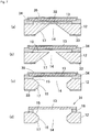
- Figs. 6(a) to (d) and Figs. 7(a) to (d) are cross-sectional views describing the manufacturing steps of the vibration sensor 31. The manufacturing steps of the vibration sensor 31 will be described below according to Figs. 6(a) to (d) and Figs. 7(a) to (d) .
- the unnecessary portion of the SiO 2 thin film is removed using the photolithography technique, so that a sacrifice layer 32 of the SiO 2 thin film forms only in the region where the thin film 13 is to be lifted from the upper surface of the Si substrate 12, as shown in Fig. 6(a) .
- a protective film 34 of SiN is then formed on the front surface of the Si substrate 12 from above the sacrifice layer 32, so that the sacrifice layer 32 is covered by the protective film 34, as shown in Fig. 6(b) .
- the thin film 13 of polycrystalline silicon is then formed on the front surface of the protective film 34, as shown in Fig. 6(c) .
- a protective film 35 of SiN is then formed on the front surface of the protective film 34 from above the thin film 13, so that the thin film 13 is covered by the protective film 35, as shown in Fig. 6(d) .
- a protective film 33 made of material other than SiO 2 is also formed on the back surface of the Si substrate 12. In this case, if the protective film 33 is formed by SiN thin film, the protective film 34 or the protective film 35 and the protective film 33 can be formed all at once in the same step.
- part of the protective film 33 is opened to a rectangular shape using the photolithography technique, thereby forming the backside etching window 26, as shown in Fig. 6(d) .
- the backside etching window 26 merely needs to have a size for crystal anisotropic etching performed from the backside etching window 26 to reach the front surface of the Si substrate 12.
- the Si substrate 12 is soaked in the etchant such as TMAH to etch the Si substrate 12 from the backside etching window 26, thereby forming the through-hole 14 in the Si substrate 12.
- TMAH etchant
- the etchant such as TMAH performs crystal anisotropic etching on the Si, and thus etching advances along the (111) plane and the crystal plane equivalent thereto at the back surface of the Si substrate 12, and ultimately the through-hole 14 reaches the front surface of the Si substrate 12 and the sacrifice layer 32 is exposed to the interior of the through-hole 14, as shown in Fig. 7(a) .
- the sacrifice layer 32 of SiO 2 is not etched by the etchant such as TMAH, and thus the etching process is terminated when the sacrifice layer 32 is exposed, and then the Si substrate 12 is washed.
- the etchant such as TMAH
- the Si substrate 12 is then soaked in the HF aqueous solution.
- the HF aqueous solution does not invade the Si substrate 12 but isotropically etches the SiO 2 , and thus the sacrifice layer 32 is etched from the exposed portion towards the periphery by the HF aqueous solution entered into the through-hole 14 from the back side of the Si substrate 12, whereby the gap 19 forms between the thin film 13 and the front surface of the Si substrate 12, as shown in Fig. 7(b) .
- the Si substrate 12 is washed, and then again soaked in the etchant such as TMAH.
- This etchant enters the gap 19 and performs crystal anisotropic etching on the Si substrate 12 from the front side.
- the corners of the Si substrate 12 are removed at the inner peripheral surface of the through-hole 14 thereby forming the inclined surface 15 and the vertical surface 16, and the through-hole 14 is etched to a shape similar to a doughnut hole, as in the first embodiment.
- the Si substrate 12 is pulled out from the etchant after the desired through-hole 14 is formed, as shown in Fig. 7(c) , and then washed and dried.
- the protective films 33, 34, 35 of SiN are removed by heated phosphoric acid aqueous solution, or the like, and the vibration sensor 31 is completed.
- the through-hole 14 of small spreading can be opened at the back side and the vibration sensor 31 can be miniaturized with only the etching from the back side of the Si substrate 12 by fabricating the vibration sensor 31 in the above manner. Furthermore, since the through-hole 14 can be opened through etching of only from the back side, the etching hole does not need to be opened in the thin film 13, and the risk of changing the physical characteristics of the thin film 13 in the vibration sensor 31 or lowering the strength of the thin film 13 is reduced.
- the opening area on the back side of the through-hole 14 is determined by the size of the backside etching window 26 opened in the protective film 33, and the opening area on the front side of the through-hole 14 is determined by the size of the sacrifice layer 32, and thus the opening area of the through-hole 14 can be accurately controlled according to the above-described manufacturing method.
- the etchant is changed between the step of performing crystal anisotropic etching of the through-hole and the step of etching the sacrifice layer, restrictions in selecting the etchant in the respective steps is reduced.
- the step management such as yield inspection can also be carried out in each etching step as continuous transition is not made from the crystal anisotropic etching to the isotropic etching.
- the crystal anisotropic etching and the isotropic etching are performed by the same etchant, and thus the crystal anisotropic etching and the isotropic etching can be continuously performed in the same device, and working efficiency is high.
- the crystal anisotropic etching and the isotropic etching are performed in separate steps, and thus the restriction in the means of crystal anisotropic etching and the means of isotropic etching is reduced, where the isotropic etching may be chemical etching using corrosive gas other than the aqueous solution.
- Fig. 8(a) is a plan view showing a structure of a vibration sensor 41 according to the third embodiment, which does not form part of the present invention
- Fig. 8(b) is a cross-sectional view taken along line X-X of Fig. 8(a)
- the vibration sensor 41 has a corrugated structure and a functional portion such as a stopper 43 arranged in the thin film 13.
- the corrugated structure of the thin film 13 is configured by two bent portions 42 having a square annular shape. Each bent portion 42 is bent such that the cross-section thereof projects to the upper side of the thin film 13. It has been reported in " The fabrication and use of micromachined corrugated silicon diaphragms" (J.H.Jerman, Sensors and Actuators A21-A23 pp.998-992, 1992 ) that a displacement of the thin film 13 increases and a deflection by stress reduces by forming the corrugated structure in the thin film 13.
- the stopper 43 is formed by projecting the front surface of the thin film 13 to a round projection shape.
- the thin film 13 becomes a movable electrode, and an opposite electrode (fixed electrode) is arranged on the upper surface of the thin film 13.
- the stopper 43 arranging the stopper 43 on the upper surface of the thin film 13 prevents the thin film 13 from being adsorbed to the opposite electrode by electrostatic force caused by charging of charges of the vibration sensor 41, capillary force caused by moisture attachment, and the like by the stopper 43 abutting on the fixed electrode even if the thin film 13 greatly deforms.
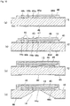
- Figs. 9(a) and (b) are views describing the manufacturing steps of the vibration sensor 41.
- the manufacturing steps of the vibration sensor 41 will be described below according to Fig. 9 to Fig. 13 .
- a sacrifice layer of polycrystalline silicon thin film is formed to a predetermined pattern on the front surface of the Si substrate 12.
- the sacrifice layer includes a square sacrifice layer 44a positioned at a central part, square annular-shaped sacrifice layers 44b, 44c formed at the forming region of the bent portion 42, a linear sacrifice layer 44d connecting the sacrifice layers 44a to 44c, and a sacrifice layer 44e formed in the forming region of the stopper 43.
- the front surface of the Si substrate 12 is covered with a protective film 45 of SiO 2 from above the sacrifice layers 44a to 44e, and a protective film 46 of SiO 2 is also formed on the back surface of the Si substrate 12.
- the protective film 45 is formed on each sacrifice layer 44a to 44e, and thus the protective film 45 is bulged upward at the portion of each sacrifice layer 44a to 44e.
- the thin film 13 of polycrystalline silicon thin film is formed on the protective film 45.
- the thin film 13 is lifted up by each sacrifice layer 44a to 44e by way of the protective film 45 at the region of each sacrifice layer 44a to 44e, and thus the bent portion 42 forms on the sacrifice layers 44b, 44c and the stopper 43 forms on the sacrifice layer 44e.
- the thin film 13 is also bulged upward on the sacrifice layers 44a and 44d, thereby forming projections 47, 48.
- a protective film 49 of SiO 2 is formed on the front surface of the protective film 45 from above the thin film 13 thereby covering the thin film 13 with the protective film 49, and a backside etching window 50 is opened in the protective film 46 at the back surface of the Si substrate 12.
- the Si substrate 12 is soaked in the etchant such as TMAH to perform crystal anisotropic etching from the backside etching window 50, thereby forming the through-hole 14 of a truncated pyramid shape at the back surface of the Si substrate 12.
- the through-hole 14 stops when the etching at the lower surface of the Si substrate 12 reaches the edge of the backside etching window 50.
- the sacrifice layer 44a is exposed to the through-hole 14 when the through-hole 14 reaches the front surface of the Si substrate 12.
- the sacrifice layer 44a is subjected to isotropic etching by the etchant such as TMAH.
- the isotropic etching starting from the sacrifice layer 44a advances from sacrifice layer 44a ⁇ sacrifice layer 44d ⁇ sacrifice layer 44b ⁇ sacrifice layer 44c as shown with thin line arrows in Fig. 11(a) .
- the crystal anisotropic etching of the Si substrate 12 advances from the edge portion of gaps 51a to 51d after the sacrifice layers 44a to 44d are removed, as shown with thick line arrows in Figs. 11(a) and (b) and Fig. 12(a) (Fig. 12(a) shows the front surface of the Si substrate 12), so that etching of the through-hole 14 is also performed from the front side of the Si substrate 12.
- the upper surface of the Si substrate 12 is etched at the region on the inner side than the outer periphery of the sacrifice layer 44c, and the through-hole 14 etched from the front side and the back side forms in the Si substrate 12.
- the sacrifice layer 44e is removed by etching in this case.
- the Si substrate 12 is pulled out from the etchant at a point the through-hole 14 is completely formed.
- the protective films 45, 49 of SiO 2 are removed by etching with HF aqueous solution, and the like, which etching is terminated at a point only the holder 18 formed from the protective film 45 remains at the four corners of the thin film 13, as shown in Figs. 13(a) and (b) , and then washing and drying are performed to complete the vibration sensor 41.
- the through-hole 14 of small spreading can be opened at the back side and the vibration sensor 41 can be miniaturized with only the etching from the back side of the Si substrate 12. Furthermore, since the through-hole 14 can be opened through etching of only from the back side, the etching hole does not need to be opened in the thin film 13, and the risk of changing the physical characteristics of the thin film 13 in the vibration sensor 41 or lowering the strength of the thin film 13 is reduced. Moreover, the corrugated structure, the stopper, and the like can be easily formed in the thin film 13 through the same step.
- Fig. 14(a) is a plan view showing a structure of a vibration sensor 61 according to the fourth embodiment, which forms part of the present invention
- Fig. 14(b) is a cross-sectional view thereof.
- the holder 18 is formed over the entire periphery of the lower surface of the thin film 13, but the holder 18 is formed only at the corners (four corners) of the thin film 13 in the vibration sensor 61 of the fourth embodiment.
- the holder 18 is arranged only at the corners of the thin film 13, and thus the upper side and the lower side of the thin film 13 are communicated through a vent hole 63 between the holders 18 of the thin film 13 at the four sides.
- Fig. 15(a) is a plan view showing a structure of another vibration sensor 62 of the fourth embodiment of the present invention
- Fig. 15(b) is a cross-sectional view thereof.
- the holder 18 is formed only at one side of the thin film 13.
- the thin film 13 is supported in a cantilever form by the holder 18, and thus the upper side and the lower side of the thin film 13 are communicated through the vent holes 63 at the three sides.
- the width of the protective film may be widened at the portion to form the holder 18, or the distance (distance from etching starting position to terminating position) from the etchant placing position may be set large to manage the etching time to thereby partially remove the protective film and partially leave the protective film, so that the holder 18 can be formed from the remained protective film.
- the holder 18 is formed at a position distant from the center in the vibration sensor 61.
- the width of the protective film at one side is made larger than the width of the protective film at the other three sides so as to remain after etching.
- the structures of the vibration sensors 61, 62 are desirable in the application of the microphone (acoustic sensor).
- the microphone acoustic sensor
- the thin film 13 is flexible and is easily elastically deformable since the thin film 13 is fixed only at one portion. Therefore, it is suitable in use as a microphone, and the like, for detecting dynamic pressure difference.
- the thin film 13 becomes a flexible spring when only the four corners of the thin film 13 are fixed as in the vibration sensor 61. Furthermore, according to such a method for fixing only four corners, the majority of the thin film 13 deforms like a parallel plate, and thus the sensitivity of an electrostatic capacity microphone enhances significantly.
- the fixed portion at the four corners of the thin film 13 preferably has a shape extended in a diagonal direction so that external stress by deformation does not concentrate.
- the electrode can be taken out from the thin film 13 without inhibiting the vibration of the thin film 13 by connecting an electrode pad 73 to the extended site.
- the vibration characteristics of the thin film 13 are changed by controlling the internal stress of the holder 18. For instance, if a tensile stress of the thin film 13 is strong, the tensile stress of the thin film 13 is weakened by forming the holder 18 as an oxide film having a compression stress, thereby enhancing the sensitivity.
- Ventilation characteristic is provided between the front surface of the Si substrate 12 and the thin film 13, and thus a static pressure difference can be eliminated at both surfaces of the thin film 13, and the function of vent hole can be provided.
- the width of the vent hole in a plane direction is set short to enhance the acoustic resistance.
- narrowing the width of the vent hole has limits in terms of process rule, and effects cannot be greatly expected.
- ⁇ is a friction loss coefficient of the vent hole
- t is a length in a ventilation direction of the vent hole
- a is an area of the diaphragm
- Sv is a cross-sectional area of the vent hole.
- Rb is a resistance component of the above equation
- Cbc is an acoustic compliance of the through-hole 14
- Csp is a stiffness constant of the thin film 13.
- the length t of the vent hole 63 between the upper surface of the Si substrate 12 and the thin film 13 can be set long in the vibration sensors 61, 62. Therefore, in the vibration sensors 61, 62, the acoustic resistance can be set very high by taking the length t of the vent hole 63 long, as apparent from equation (1), and the low frequency characteristic of the vibration sensors 61, 62 can be improved, as apparent from equation (2), and thus preferable characteristics for the microphone can be obtained.
- Vbc is a volume of the through-hole (back chamber volume)
- ⁇ c 2 is volume elasticity of air
- Sbc is an opening area of the through-hole 14.
- the through-hole 14 having a small opening area compared to the volume can be formed by etching from both front and back surfaces of the Si substrate 12, and thus the acoustic compliance of the through-hole 14 can be increased and the sensitivity is prevented from easily lowering even if the vent hole 63 is opened, as apparent from equation (3).
- the etching is ultimately advanced to the state of Fig. 17(c) through the state of Fig. 17(b) , and the etching of the through-hole 14 is stopped when the (111) plane or the crystal plane equivalent thereto appears. Therefore, the volume of the through-hole 14 becomes larger, and the acoustic compliance Ccav is further increased by etching to the state of Fig. 17(c) .
- the appropriate volume of the through-hole 14 and the size of the vibration sensor can be obtained by controlling the etching time when etching from the state of Fig. 17(a) to the state of Fig. 17(c) .
- the state of Fig. 17(c) is the final mode of the crystal anisotropic etching, and the shape of the back chamber is determined by the size and the relative position of the opening at the front surface and the back surface.
- the shape of the back chamber (through-hole 14) is maintained substantially constant even if the etching time is further extended, and thus process stability is satisfactory and a yield is high.
- Fig. 18(a) is a plan view of the microphone 71
- Fig. 18(b) is a plan view of the microphone 71 (i.e., vibration sensor 61) with a back plate 72 removed
- Fig. 19 is a cross-sectional view of the microphone 71.
- the microphone 71 has the back plate 72 fixed on the vibration sensor 61 so as to cover the thin film 13.
- the back plate 72 has a cap-shape with a recessed portion at the lower surface, and is fixed on the front surface of the Si substrate 12 so as to accommodate the thin film 13 in the recessed portion.
- a gap of an extent of not inhibiting the vibration of the thin film 13 forms between the lower surface of the back plate 72 and the thin film 13.
- a metal electrode 73 is arranged on the upper surface of the back plate 72.
- the metal electrode 73 is not arranged on the entire surface of the back plate as shown in Fig. 18 , but is arranged at one portion of the back plate 72 and in particular, at the portion facing the portion where the amplitude is relatively large of the thin film 13. This is to reduce the parasitic capacitance, and enhance the characteristic of the electrostatic capacity microphone 71. If the thin film 13 is fixed at four corners as in the present embodiment, the parasitic capacitance can be reduced and the limited region can be effectively utilized by having the shape of the metal electrode 73 to a substantially octagonal shape as shown in Fig. 18(a) .
- a plurality of acoustic holes 74, 75 is opened in the metal electrode 73 and the back plate 72. Therefore, the acoustic vibration from the upper side passes through the acoustic holes 74, 75 of the metal electrode 73 and the back plate 72 and reaches the thin film 13, thereby vibrating the thin film 13.
- the thin film 13 (movable electrode) of polycrystalline silicon has conductivity, and the electrostatic capacity between the thin film 13 and the metal electrode 73 (fixed electrode) changes when the thin film 13 vibrates, which can be retrieved to the outside as an electric signal through an electrode pad 76 on the thin film 13 side and an electrode pad 77 on the back plate side 72 side, and the acoustic vibration can be detected by detecting such change in electrostatic capacity.
- the manufacturing steps of the microphone 71 will be described according to Figs. 20(a) to (d) and Figs. 21(a) to (d) .
- the protective film 20, the sacrifice layer 23, the protective film 24, the thin film 13, and the protective film 25 are sequentially stacked on the front surface of the Si substrate 12, and the protective film 21 is formed on the back surface of the Si substrate 12.
- This is the same structure as Fig. 3(a) of the first embodiment and is fabricated through the same steps as Fig. 2(a) to Fig. 2(d) of the first embodiment.
- an SiN film is formed from the front surface of the protective film 25 to the outer peripheral surfaces of the protective films 24 and 25, and the back plate 72 is formed by the SiN film.
- the acoustic hole 75 is opened in the back plate 72 by etching.
- the SiN film at the electrode retrieving portion is also etched. Then, as shown in Fig.
- a Cr film is formed on the front surface of the back plate 72, and Au is formed thereon to thereby obtain an Au/Cr film, and the Au/Cr film is etched to a predetermined shape to fabricate the metal electrode 73 and the electrode pads 76, 77.
- the backside etching window 26 is opened in the protective film 21 at the back surface using the photolithography technique.
- the size of the backside etching window 26 of about 570 ⁇ m for one side is sufficient in a case of the (100) plane Si substrate 12 having a thickness of 400 ⁇ m.
- the Si substrate 12 is soaked in the etchant such as TMAH to perform crystal anisotropic etching on the Si substrate 12 from the back side, thereby opening the through-hole 14 in the Si substrate 12. This state is shown in Fig. 21(a) .
- the polycrystalline silicon sacrifice layer 23 is subjected to isotropic etching by the etchant such as TMAH, and the gap 19 forms at the front surface of the Si substrate 12, as shown in Fig. 21(b) .
- the etchant such as TMAH enters the gap 19 thereby etching the Si substrate 12 also from the front side, and the etching advances also in the horizontal direction, whereby the edge of the through-hole 14 has a cross-sectional shape tapered at the front and the back, as shown in Fig. 21(c) .
- the Si substrate 12 is pulled out from the etchant when the desired shape of the through-hole 14 is obtained.
- the protective films 21, 24, 25 protecting the thin film 13 are then etched with HF aqueous solution, or the like, and removed leaving the protective film 20 at the lower surface of the back plate 72 and the holder 18.
- the protective film 25 is mainly etched with the HF aqueous solution entered from the acoustic holes 74, 75. Therefore, the arrangement interval of the acoustic holes 74, 75 is desirably a substantially equal interval so that etching is uniformly performed, as shown in Fig. 18(a) .
- the etching time can be reduced by reducing the arrangement interval, but the number of acoustic holes 74, 75 increases by such amount, the electrode area reduces, and the sensitivity lowers. Furthermore, the arrangement interval of the acoustic holes is also related to the size of the holder 18. In other words, if the arrangement interval is too large, the etching time becomes long, and all the holders 18 are etched. In view of the above, the interval of the acoustic holes 74, 75 is set to 50 ⁇ m. The holder 18 is formed only at the corner of the thin film 13, and the vent hole 63 is opened between the holders 18. The microphone 71 having the structure of Fig. 20(d) is thereby completed.
- the through-hole 14 can be etched from both the front side and the back side of the Si substrate 12, an area loss due to the inclined surfaces of the through-hole 14 can be reduced, and the microphone 71 can be miniaturized by fabricating the microphone 71 in the above manner. Furthermore, starting the etching from the back side, the Si substrate 12 can be subjected to crystal anisotropic etching from the front side and the back side to open the through-hole 14 by combining the crystal anisotropic etching and the isotropic etching. Therefore, the through-hole 14 can be opened through simple steps, and both lower cost and high productivity can be achieved. Moreover, since the etching hole does not need to be opened in the thin film 13, the risk of lowering the strength of the thin film 13 or degrading the vibration characteristic is also reduced.
- the thin film 13 easily vibrates and the sensitivity of the microphone 71 improves since the thin film 13 is partially supported by the holder 18, and the acoustic resistance of the microphone 71 increases and the low frequency characteristic improves since the long vent hole 63 is formed in the gap between the thin film 13 and the Si substrate 12 between the holders 18. Furthermore, the acoustic compliance can be increased and the characteristic of the microphone 71 can be improved since the volume of the through-hole 14 can be increased.
- the backside etching window 26 is opened in the protective film 21 at the back surface using the photolithography technique.
- the size of the backside etching window 26 of about 570 ⁇ m for one side is sufficient in a case of the (100) plane Si substrate 12 having a thickness of 400 ⁇ m.
- the Si substrate 12 is soaked in the etchant such as TMAH to perform crystal anisotropic etching on the Si substrate 12 from the back side, thereby opening the through-hole 14 in the Si substrate 12. This state is shown in Fig. 21(a) .
- the polycrystalline silicon sacrifice layer 23 is subjected to isotropic etching by the etchant such as TMAH, and the gap 19 forms at the front surface of the Si substrate 12, as shown in Fig. 21(b) .
- the etchant such as TMAH enters the gap 19 thereby etching the Si substrate 12 also from the front side, and the etching advances also in the horizontal direction, whereby the edge of the through-hole 14 has a cross-sectional shape tapered at the front and the back, as shown in Fig. 21(c) .
- the Si substrate 12 is pulled out from the etchant when the desired shape of the through-hole 14 is obtained.
- the protective films 21, 24, 25 protecting the thin film 13 are then etched with HF aqueous solution, or the like, and removed leaving the protective film 20 at the lower surface of the back plate 72 and the holder 18.
- the protective film 25 is mainly etched with the HF aqueous solution entered from the acoustic holes 74, 75. Therefore, the arrangement interval of the acoustic holes 74, 75 is desirably a substantially equal interval so that etching is uniformly performed, as shown in Fig. 18(a) .
- the etching time can be reduced by reducing the arrangement interval, but the number of acoustic holes 74, 75 increases by such amount, the electrode area reduces, and the sensitivity lowers. Furthermore, the arrangement interval of the acoustic holes is also related to the size of the holder 18. In other words, if the arrangement interval is too large, the etching time becomes long, and all the holders 18 are etched. In view of the above, the interval of the acoustic holes 74, 75 is set to 50 ⁇ m. The holder 18 is formed only at the corner of the thin film 13, and the vent hole 63 is opened between the holders 18. The microphone 71 having the structure of Fig. 20(d) is thereby completed.
- the through-hole 14 can be etched from both the front side and the back side of the Si substrate 12, an area loss due to the inclined surfaces of the through-hole 14 can be reduced, and the microphone 71 can be miniaturized by fabricating the microphone 71 in the above manner. Furthermore, starting the etching from the back side, the Si substrate 12 can be subjected to crystal anisotropic etching from the front side and the back side to open the through-hole 14 by combining the crystal anisotropic etching and the isotropic etching. Therefore, the through-hole 14 can be opened through simple steps, and both lower cost and high productivity can be achieved. Moreover, since the etching hole does not need to be opened in the thin film 13, the risk of lowering the strength of the thin film 13 or degrading the vibration characteristic is also reduced.
- the thin film 13 easily vibrates and the sensitivity of the microphone 71 improves since the thin film 13 is partially supported by the holder 18, and the acoustic resistance of the microphone 71 increases and the low frequency characteristic improves since the long vent hole 63 is formed in the gap between the thin film 13 and the Si substrate 12 between the holders 18. Furthermore, the acoustic compliance can be increased and the characteristic of the microphone 71 can be improved since the volume of the through-hole 14 can be increased.
Landscapes
- Engineering & Computer Science (AREA)
- Physics & Mathematics (AREA)
- Acoustics & Sound (AREA)
- Signal Processing (AREA)
- Manufacturing & Machinery (AREA)
- Microelectronics & Electronic Packaging (AREA)
- Pressure Sensors (AREA)
- Electrostatic, Electromagnetic, Magneto- Strictive, And Variable-Resistance Transducers (AREA)
- Weting (AREA)
Description
- The present invention relates to a vibration sensor and a method for manufacturing the same, in particular, to a vibration sensor including a thin film such as a diaphragm and a method for manufacturing the same.
- A vibration sensor in which a thin film is formed by stacking layers of monocrystalline silicon or polycrystalline silicon on a silicon substrate, and the thin film is used as a diaphragm, is being developed by applying a semiconductor integrated circuit manufacturing technique. The diaphragm made of silicon has a small internal stress and a low density compared to metal such as aluminum and titanium, and thus a vibration sensor of high sensitivity can be obtained and compliance with a semiconductor integrated circuit manufacturing step is also satisfactory. The vibration sensor including such a diaphragm includes a capacitor microphone disclosed in Patent Document 1. In such a capacitor microphone, a diaphragm (movable electrode) and a fixed electrode are formed on a front surface of a semiconductor substrate of a monocrystalline silicon (100) plane, and thereafter, an etching mask is formed at the outer peripheral part of a back surface of the relevant semiconductor substrate, and the semiconductor substrate is etched from the back side until reaching the front surface thereby forming a through-hole at a central part of the semiconductor substrate. As a result, the diaphragm has a periphery fixed to the front surface of the semiconductor substrate and the central part supported in a hollow state above the through-hole, and thus can be vibrated by audio vibration and the like.
- However, in the capacitor microphone of such a structure, an inclined surface from a (111) plane appears at the inner peripheral surface of the through-hole since the (100) plane semiconductor substrate is subjected to crystal anisotropic etching from the back side, and the through-hole becomes a space of a truncated pyramid shape opened large to the back side. Thus, the opening area at the back side of the through-hole becomes large compared to the area of the diaphragm, and miniaturization of the capacitor microphone is difficult. If the thickness of the semiconductor substrate is reduced, the ratio of the opening area of the back surface with respect to the opening area of the front surface of the through-hole can be reduced, but the strength of the semiconductor substrate lowers and handling at the time of manufacturing becomes difficult, and thus reducing the thickness of the semiconductor substrate has limits.
- In a film-type sensor described in Patent Document 2, a through-hole is opened in the semiconductor substrate from the back side by vertical etching such as a so-called DRIE (Deep Reactive Ion Etching) and ICP (Inductively Coupled Plasma). Therefore, the film-type sensor can be miniaturized by an amount the through-hole does not spread in the truncated pyramid shape. However, in devices of DRIE, ICP, and the like, a price of the device is high and processing of a wafer is in sheet form, and thus productivity is not satisfactory.
- A method for performing crystal anisotropic etching on the semiconductor substrate from the front side (diaphragm side) is also known, but in such a method, an etching hole needs to be opened in the diaphragm, which etching hole sometimes adversely affects vibration characteristics, strength, and the like of the diaphragm.
- An etching method for forming a through-hole in the substrate by performing crystal anisotropic etching on the (100) plane semiconductor substrate from the back side, and reducing the ratio of the opening area of the back surface with respect to the opening area of the front surface includes a method described in Patent Document 3. In such a method, a sacrifice layer is first formed in a rectangular region to be opened on the front surface of the silicon wafer or the semiconductor substrate, and a thin film of silicon nitride is vapor deposited thereon, and thus the opening area of the back surface of the silicon wafer merely needs to be a size the through-hole can reach the sacrifice layer by anisotropic etching.
- However, in this etching method, the thin film is exposed to an etchant of the substrate when etching the substrate of after the sacrifice layer of the front surface is etched, and thus monocrystalline silicon and polycrystalline silicon cannot be used for the material of the thin film. Furthermore, since the thin film is directly formed on the substrate, steps and structures for enhancing the characteristics of the vibration sensor such as stress control of the thin film and vent hole become difficult to incorporate. Therefore, the etching method disclosed in Patent Document 3 is not suitable for the method for manufacturing the vibration sensor requiring high sensitivity such as microphone.
Patent Document 4 describes a semiconductor component comprising a substrate, two flexible pressure sensor diaphragms supported by the substrate, and a fixed electrode between the two diaphragms. The two diaphragms and the fixed electrode are electrodes of two differential capacitors. The substrate has a hole extending from one surface of the substrate to an opposite surface of the substrate. The hole is located underneath the two diaphragms, and the hole at the opposite surfaces of the substrate is preferably larger than the hole at an interior portion of the substrate.
Patent Document 5 describes that on an upper plane of a silicon substrate, a vibrating electrode plate is formed through an insulating film. On the vibrating electrode plate, a counter electrode plate is arranged through an insulating film, and an acoustic hole penetrates the counter electrode plate. On the vibrating electrode plate and the counter electrode plate, semi-elliptical holes are opened to vertically face each other. On the upper plane of the silicon substrate, a recessed part having a truncated pyramid shape is formed by etching through the etching holes. The vibrating electrode plate is held to the silicon substrate by a holding part between the etching holes.
Non-patent Document 1 describes a silicon condenser microphone with a corrugated diaphragm. The microphone is fabricated on a single wafer by use of silicon anisotropic etching and sacrificial layer etching techniques, so that no bonding techniques are required. -
- Patent Document 1: Japanese Unexamined Patent Publication No.
2004-506394 - Patent Document 2: Japanese Unexamined Patent Publication No.
2003-530717 - Patent Document 3: Japanese Unexamined Patent Publication No.
1 -309384 - Patent Document 4 :
US 6 426 239 B1 - Patent Document 5 :
WO 2006/049100 A1 - Non-patent Document 1 : QUANBO ZOU ET AL, "Design and Fabrication of Silicon Condenser Microphone Using Corrugated Diaphragm Technique", JOURNAL OF MICROELECTROMECHANICAL SYSTEMS, IEEE SERVICE CENTER, US, vol. 5, no. 3, 1 September 1996, XP011034717, ISSN: 1057-7157, DOI:10.1109/84.536626
- In view of the technical problems described above, it is an object of the present invention to provide a vibration sensor that is small, has high productivity, and excels in vibration characteristic, and a method for manufacturing the same.
- A method for manufacturing a vibration sensor of the present invention includes: forming, at one part of a front surface of a semiconductor substrate of monocrystalline silicon, a sacrifice layer with a material isotropically etched by an etchant for etching the semiconductor substrate; forming a thin film protective film with a material having resistance to the etchant on the sacrifice layer and the front surface of the semiconductor substrate at a periphery of the sacrifice layer; forming a thin film of monocrystalline silicon, polycrystalline silicon, or amorphous silicon on an upper side of the sacrifice layer; opening a backside etching window in a back surface protective film having resistance to the etchant for etching the semiconductor substrate formed on a back surface of the semiconductor substrate; forming a through-hole in the semiconductor substrate by etching the semiconductor substrate anisotropically by using crystal -oriented etching by applying the etchant from the back surface window, then etching the sacrifice layer isotropically by the etchant after the etchant reaches the front surface of the semiconductor substrate, and then etching the semiconductor substrate anisotropically by using crystal-oriented etching from a front side by the etchant spread to a space formed after the sacrifice layer is removed; and forming at least one vent hole for putting the front side in communication with the back side of the thin film and at least one holder for supporting the thin film on an upper surface of the semiconductor substrate by removing the thin film protective film partially.
- According to the method for manufacturing the vibration sensor of the present invention, the through-hole is formed by performing crystal anisotropic etching on the semiconductor substrate of monocrystalline silicon from both front and back surfaces, and thus the opening area of the through-hole does not become too large compared to the area of the thin film, and the vibration sensor can be miniaturized. Therefore, the number of elements that can be fabricated from one wafer increases, and the cost of the vibration sensor can be lowered. According to the method for manufacturing the vibration sensor, the through-hole can be formed from both surfaces through one etching step, and thus the manufacturing steps are simplified. Moreover, since the protective layer is formed between the sacrifice layer and the thin film, the thin film is prevented from being damaged by the etchant when forming the through-hole even if the thin film is made of a material that does not have resistance to the etchant of the semiconductor substrate. A vibration sensor of high productivity and high sensitivity can be obtained since the thin film is formed by monocrystalline silicon, polycrystalline silicon, or amorphous silicon.
- The method for manufacturing the vibration sensor includes forming a vent hole for communicating the front side and the back side of the thin film between the holders. According to the method for manufacturing the vibration sensor of the present invention, a vent hole of a long length can be formed, and thus an acoustic resistance can be increased and satisfactory acoustic characteristics can be obtained when used in a microphone, and the like. Furthermore, an electrostatic pressure at the front and the back of the thin film can be balanced since the front side and the back side of the thin film are communicated with the vent hole.
- In an embodiment of the method for manufacturing the vibration sensor, the thin film is a square. According to such an embodiment, the opening formed by performing crystal anisotropic etching of the monocrystalline silicon substrate can be effectively used.
- In another embodiment of the method for manufacturing the vibration sensor, the holder is arranged at four corners of the thin film. According to such a configuration, the sensitivity of the vibration enhances since the thin film can flexibly deform.
- In still another embodiment of the method for manufacturing the vibration sensor, the sacrifice layer is arranged at one part of the forming region of the thin film so that the thin film is bendable. According to such an embodiment, a displacement of the thin film can be increased and a deflection by stress can be reduced.
- In yet another embodiment of the method for manufacturing the vibration sensor, the sacrifice layer is arranged at one part of the forming region of the thin film to form a projection on the front surface of the thin film. According to such an embodiment, the deformed thin film is prevented from area contacting and attaching to the electrode, and the like, when the electrode, and the like are arranged on the upper side of the thin film.
- In yet another embodiment of the method for manufacturing the vibration sensor of the present invention, an area of the cross-section parallel to the opening at the interior of the through-hole is larger than the opening area of the front surface of the through-hole. According to such an embodiment, a volume of the through-hole can be increased, and thus acoustic compliance can be increased when the vibration sensor is used in the acoustic sensor.
- In another embodiment of the method for manufacturing the vibration sensor of the present invention, the sacrifice layer is made of polycrystalline silicon or amorphous silicon. According to such an embodiment, the sacrifice layer can be simultaneously etched when etching the semiconductor substrate of monocrystalline silicon, whereby the steps can be simplified. Since the polycrystalline silicon and the amorphous silicon have high temperature resistance, high temperature process can be used in the post-step, and the compliance with the semiconductor integrated circuit manufacturing step is also satisfactory.
According to the method for manufacturing the vibration sensor, the semiconductor substrate can be subjected to crystal anisotropic etching from both the front and the back surfaces starting from the crystal anisotropic etching of the semiconductor substrate from the back side, and thus an etching hole does not need to be formed in the thin film, and a risk of lowering the strength of the thin film or changing the characteristics of the thin film is eliminated. Furthermore, according to the method for manufacturing the vibration sensor, the manufacturing steps are simplified as the through-hole can be formed from both surfaces in one etching step. - A vibration sensor manufactured according to the above-mentioned method of the present invention includes: a semiconductor substrate of monocrystalline silicon formed with a through-hole passing from front to back; at least one holder made of a material having resistance to an etchant for forming the through-hole by etching the semiconductor substrate, and arranged on a front surface of the semiconductor substrate; a thin film having corners supported by the holder, and covering an opening on the substrate front surface side of the through-hole; and at least one vent hole for putting the front side in communication with the back side of the thin film; wherein an area of a cross-section parallel to the substrate front surface of the through-hole gradually decreases or increases from the front surface towards a back surface of the semiconductor substrate, and changes from decrease to increase or from increase to decrease at a middle of the front surface and the back surface of the semiconductor substrate, and the at least one vent hole is formed by a thin film protective film.
- According to the vibration sensor of the present invention, the area of the cross-section parallel to the substrate front surface of the through-hole gradually decreases or increases from the front surface towards the back surface of the semiconductor substrate, and changes from decrease to increase or from increase to decrease at a middle of the front surface and the back surface of the semiconductor substrate, and thus the ratio of the opening area of the through-hole at the front surface of the semiconductor substrate and the opening area of the through-hole at the back surface approaches one, and the vibration sensor can be miniaturized. Since the volume of the through-hole can be increased, the acoustic compliance can be increased when using the vibration sensor in the acoustic sensor.
- The configuring elements described above in the present invention may be arbitrarily combined as much as possible.
-
-
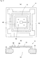
Fig. 1(a) is a plan view showing a structure of a vibration sensor according to a first embodiment, which does not form part of the present invention, andFig. 1(b) is a cross-sectional view thereof. -
Figs. 2(a) to (d) are cross-sectional views describing manufacturing steps of the vibration sensor of the first embodiment. -
Figs. 3(a) to (d) are cross-sectional views describing the manufacturing steps of the vibration sensor of the first embodiment, followingFig. 2(d) . -
Figs. 4(a) to (c) are cross-sectional views describing the manufacturing steps of the vibration sensor of the first embodiment, followingFig. 3(d) . -
Fig. 5(a) is a plan view showing a vibration sensor according to a second embodiment, which does not form part of the present invention, andFig. 5(b) is a cross-sectional view thereof. -
Figs. 6(a) to (d) are cross-sectional views describing manufacturing steps of the vibration sensor of the second embodiment. -
Figs. 7(a) to (d) are cross-sectional views describing the manufacturing steps of the vibration sensor of the second embodiment, followingFig. 6(d) . -
Fig. 8(a) is a plan view showing a structure of a vibration sensor according to a third embodiment, which does not from part of the present invention, andFig. 8(b) is a cross-sectional view taken along line X-X ofFig. 8(a) . -
Figs. 9(a) and (b) are a plan view and a cross-sectional view describing manufacturing steps of the vibration sensor of the third embodiment. -
Figs. 10(a) to (d) are cross-sectional views describing the manufacturing steps of the vibration sensor of the third embodiment, followingFig. 9 . -
Figs. 11(a) and (b) are a plan view and a cross-sectional view describing the manufacturing steps of the vibration sensor of the third embodiment, followingFig. 10(d) . -
Figs. 12(a) and (b) are a plan view and a cross-sectional view describing the manufacturing steps of the vibration sensor of the third embodiment, followingFig. 11 . -
Figs. 13(a) and (b) are a plan view and a cross-sectional view describing the manufacturing steps of the vibration sensor of the third embodiment, followingFig. 12 . -
Fig. 14(a) is a plan view showing a structure of a vibration sensor according to a fourth embodiment, which forms part of the present invention, andFig. 14(b) is a cross-sectional view thereof. -
Fig. 15(a) is a plan view showing a structure of another vibration sensor according to the fourth embodiment of the present invention, andFig. 15(b) is a cross-sectional view thereof. -
Fig. 16 is a view describing an operation of a vent hole. -
Figs. 17(a), (b), and (c) are cross-sectional views showing the steps of continuing etching until an inner peripheral surface of a through-hole is recessed. -
Fig. 18(a) is a plan view of a microphone, which does not form part of the present invention, andFig. 18(b) is a plan view of the microphone with aback plate 72 removed. -
Fig. 19 is a cross-sectional view of the microphone: -
Figs. 20(a) to (d) are cross-sectional views showing manufacturing steps of the microphone which does not form part of the present invention. -
Figs. 21(a) to (d) are cross-sectional views showing the manufacturing steps of the microphone which does not form part of the present invention, followingFig. 20(d) . -
- 11
- Vibration sensor
- 12
- Si substrate
- 13
- Thin film
- 14
- Through-hole
- 18
- Holder
- 20, 21
- Protective film
- 22
- Etching window
- 23
- Sacrifice layer
- 24, 25
- Protective film
- 26
- Backside etching window
- 31
- Vibration sensor
- 32
- Sacrifice layer
- 33
- Protective film
- 41
- Vibration sensor
- 42
- Bent portion
- 43
- Stopper
- 44a to 44e
- Sacrifice layer
- 45, 46
- Protective film
- 49
- Protective film
- 50
- Backside etching window
- 71
- Microphone
- 72
- Back plate
- 73
- Metal electrode
- 74
- Acoustic hole
- 75
- Acoustic hole
- Embodiments of the present invention will now be described in detail below according to the drawings. It should be recognized that the present invention is not limited to the following embodiments.
-
Fig. 1(a) is a plan view showing a structure of avibration sensor 11 according to a first embodiment, which does not form part of the present invention, andFig. 1(b) is a cross-sectional view thereof. Thevibration sensor 11 is used in an acoustic sensor such as a semiconductor microphone and an ultrasonic sensor, a thin film filter, and the like. Thevibration sensor 11 includes anSi substrate 12, and a thin film 13 (diaphragm). TheSi substrate 12 is a (100) plane substrate. TheSi substrate 12 is etched from the back side so as to form a rectangular through-hole 14, which is passed through from the front to the back and which side in each horizontal and vertical direction lies in the (110) direction. The through-hole 14 has inclinedsurfaces vertical surface 16 is formed between theinclined surfaces vertical surface 16 is actually configured by a plurality of crystal planes such as a (110) plane, a (311) plane, and a (411) plane, but is shown as a vertical plane for simplification. Therefore, the cross-section of the substrate at the edge of the through-hole 14 has a shape tapered at the front and the back. - The
thin film 13 is arranged on the upper surface of theSi substrate 12 so as to cover the opening on the front side of the through-hole 14, and the entire periphery of the lower surface is fixed to the upper surface of theSi substrate 12 by aholder 18. Anarrow gap 19 forms between the opening on the front side (or surface that was the front surface of the Si substrate 12) of the through-hole 14 and the back surface of thethin film 13 by theholder 18. - According to the
vibration sensor 11 of such a structure, although the through-hole 14 is formed by etching theSi substrate 12 from the back side, the opening area on the back side does not become too large compared to the opening on the front side of the through-hole 14. Therefore, the area of theSi substrate 12 does not become large by the through-hole 14 as in the first related art. TheSi substrate 12 merely needs to have a size capable of mounting thethin film 13 and circuit components, as necessary, and thevibration sensor 11 can be miniaturized. - Manufacturing steps of the
vibration sensor 11 will now be described according toFigs. 2(a) to (d) ,Figs. 3(a) to (d) , andFigs. 4(a) to (c) . It should be noted that although a multiple number of thevibration sensors 11 is manufactured at once on a wafer, only onevibration sensor 11 will be shown and described in the following description. - First, as shown in
Fig. 2(a) ,protective films plane Si substrate 12 through thermal oxidation method, and the like. Theprotective film 20 at a region to form thegap 19 is then partially removed using a photolithography technique at the front surface of theSi substrate 12, thereby opening arectangular etching window 22. - A polycrystalline silicon thin film is formed on the front surface of the
Si substrate 12 from above theprotective film 20, and the polycrystalline silicon thin film on theprotective film 20 is removed using the photolithography technique. Arectangular sacrifice layer 23 of polycrystalline silicon thin film thereby forms on the front surface of theSi substrate 12 in theetching window 22. This state is shown inFig. 2(b) . - A
protective film 24 of SiO2 is then formed on the front surface of theSi substrate 12 from above thesacrifice layer 23, so that thesacrifice layer 23 is covered by theprotective film 24, as shown inFig. 2(c) . - A polycrystalline silicon thin film is then formed on the
protective film 24, and the unnecessary portion of the polycrystalline silicon thin film is removed using the photolithography technique, so that thethin film 13 of polycrystalline silicon thin film forms on theprotective film 24, as shown inFig. 2(d) . Furthermore, as shown inFig. 3(a) , a rectangularprotective film 25 of SiO2 is formed on thethin film 13, so that thethin film 13 is covered by theprotective film 25. - Thereafter, as shown in
Fig. 3(b) , part of theprotective film 21 is partially removed using the photolithography technique at the back surface of theSi substrate 12, thereby opening abackside etching window 26 to a rectangular shape in theprotective film 21. Thebackside etching window 26 merely needs to have a size for crystal anisotropic etching started from thebackside etching window 26 to reach the front surface of theSi substrate 12, where a relatively smallbackside etching window 26 having one side of about 570 µm is enough for theSi substrate 12 having a thickness of 400 µm. The dimension of the vertical and horizontal size of thesacrifice layer 23 is determined by the dimension of the vertical and horizontal size of the necessarythin film 13, and one side is about 650 µm, for example. - After the
backside etching window 26 is opened, etching is performed from thebackside etching window 26 by soaking in etchant such as TMAH, KOH, or EDP (hereinafter referred to as etchant such as TMAH). The etchant such as TMAH performs crystal anisotropic etching on the Si, and thus etching advances along the (111) plane and the crystal plane (inclined surface 17) equivalent thereto at the back surface of theSi substrate 12, thereby forming the through-hole 14 having a truncated pyramid shape at the back surface of theSi substrate 12. - When the through-
hole 14 reaches the front surface of theSi substrate 12 in such a manner, thesacrifice layer 23 is exposed to the interior of the through-hole 14, as shown inFig. 3(c) . Theprotective films sacrifice layer 23 of polycrystalline silicon is subjected to isotropic etching by the etchant such as TMAH. Thus, when thesacrifice layer 23 is exposed to the interior of the through-hole 14, etching proceeds from the portion exposed in the through-hole 14 towards the periphery, thereby forming thegap 19 between theprotective film 24 and the front surface of theSi substrate 12, as shown inFig. 3(d) . - In this state, the
thin film 13 and theprotective films Si substrate 12 by thegap 19, and thus can function as thin films. However, since thegap 19 is a space of thin thickness, damping effect occurs when thethin film 13 and theprotective films thin film 13 and theprotective films Si substrate 12. To prevent such drawbacks, etching of theSi substrate 12 is further continued at the lower side of thethin film 13. - It should be noted that thicker the thickness of the gap 19 (sacrifice layer 23), an etching rate becomes faster, but if too thick, formation time of the
sacrifice layer 23 becomes longer or a covering property of theprotective film 24 degrades. Thus the thickness is designed in view of the above, and is, for example, about 1 µm. The thickness of thethin film 13 is designed in view of the trade-off with the sensitivity and the strength of thevibration sensor 11, and is, for example, about 1 µm. - When the
gap 19 is created between theprotective film 24 and the front surface of theSi substrate 12, the etchant enters thegap 19, and performs crystal anisotropic etching on theSi substrate 12 from the front side. In such anisotropic etching, etching advances in the direction shown by the arrow inFig. 4(a) , thereby forming theinclined surface 15 in the through-hole 14. Furthermore, since the etching rate is large at the pointed end portion of the edge of the through-hole 14, corners are removed at the inner peripheral surface of the through-hole 14 thereby forming thevertical surface 16, and the through-hole 14 is etched to a shape similar to a doughnut hole. TheSi substrate 12 is pulled out from the etchant at a point thesacrifice layer 23 is completely etching-removed, as shown inFig. 4(b) . - After washing the
Si substrate 12, theprotective films holder 18 made from part of theprotective films vibration sensor 11 is completed, as shown inFig. 4(c) . - The through-
hole 14 of small spreading can be opened at the back side and thevibration sensor 11 can be miniaturized with only the etching from the back side of theSi substrate 12 by fabricating thevibration sensor 11 in the above manner. Furthermore, since the through-hole 14 can be opened through etching of only from the back side, the etching hole does not need to be opened in thethin film 13, and a risk of changing physical characteristics of thethin film 13 in thevibration sensor 11 or lowering the strength of thethin film 13 is reduced. - The opening area on the back side of the through-
hole 14 is determined by the size of thebackside etching window 26 opened in theprotective film 21, and the opening area on the front side of the through-hole 14 is determined by the size of thesacrifice layer 23, and thus the opening area of the through-hole 14 can be accurately controlled according to the above-described manufacturing method. - In the above embodiment, the
sacrifice layer 23 is made of polycrystalline silicon, but amorphous silicon may also be used. -
Fig. 5(a) is a plan view showing avibration sensor 31 according to the second embodiment, which does not form part of the present invention, andFig. 5(b) is a cross-sectional view thereof. In thevibration sensor 31, thethin film 13 of polycrystalline silicon is formed on theSi substrate 12 so as to cover the upper surface of the through-hole 14. Thethin film 13 has the lower surface of the outer peripheral part supported by theholder 18 at the upper surface of theSi substrate 12 and is lifted from the upper surface of theSi substrate 12, where a region surrounded by theholder 18 is deformable. -
Figs. 6(a) to (d) andFigs. 7(a) to (d) are cross-sectional views describing the manufacturing steps of thevibration sensor 31. The manufacturing steps of thevibration sensor 31 will be described below according toFigs. 6(a) to (d) andFigs. 7(a) to (d) . - First, after forming the SiO2 thin film on the upper surface of the
Si substrate 12, the unnecessary portion of the SiO2 thin film is removed using the photolithography technique, so that asacrifice layer 32 of the SiO2 thin film forms only in the region where thethin film 13 is to be lifted from the upper surface of theSi substrate 12, as shown inFig. 6(a) . - A
protective film 34 of SiN is then formed on the front surface of theSi substrate 12 from above thesacrifice layer 32, so that thesacrifice layer 32 is covered by theprotective film 34, as shown inFig. 6(b) . Thethin film 13 of polycrystalline silicon is then formed on the front surface of theprotective film 34, as shown inFig. 6(c) . - A
protective film 35 of SiN is then formed on the front surface of theprotective film 34 from above thethin film 13, so that thethin film 13 is covered by theprotective film 35, as shown inFig. 6(d) . Aprotective film 33 made of material other than SiO2 is also formed on the back surface of theSi substrate 12. In this case, if theprotective film 33 is formed by SiN thin film, theprotective film 34 or theprotective film 35 and theprotective film 33 can be formed all at once in the same step. After theprotective film 33 is formed on the back surface of theSi substrate 12, part of theprotective film 33 is opened to a rectangular shape using the photolithography technique, thereby forming thebackside etching window 26, as shown inFig. 6(d) . Thebackside etching window 26 merely needs to have a size for crystal anisotropic etching performed from thebackside etching window 26 to reach the front surface of theSi substrate 12. - After the
backside etching window 26 is opened, theSi substrate 12 is soaked in the etchant such as TMAH to etch theSi substrate 12 from thebackside etching window 26, thereby forming the through-hole 14 in theSi substrate 12. The etchant such as TMAH performs crystal anisotropic etching on the Si, and thus etching advances along the (111) plane and the crystal plane equivalent thereto at the back surface of theSi substrate 12, and ultimately the through-hole 14 reaches the front surface of theSi substrate 12 and thesacrifice layer 32 is exposed to the interior of the through-hole 14, as shown inFig. 7(a) . - The
sacrifice layer 32 of SiO2 is not etched by the etchant such as TMAH, and thus the etching process is terminated when thesacrifice layer 32 is exposed, and then theSi substrate 12 is washed. - The
Si substrate 12 is then soaked in the HF aqueous solution. The HF aqueous solution does not invade theSi substrate 12 but isotropically etches the SiO2, and thus thesacrifice layer 32 is etched from the exposed portion towards the periphery by the HF aqueous solution entered into the through-hole 14 from the back side of theSi substrate 12, whereby thegap 19 forms between thethin film 13 and the front surface of theSi substrate 12, as shown inFig. 7(b) . - After the
sacrifice layer 32 is completely removed by etching, theSi substrate 12 is washed, and then again soaked in the etchant such as TMAH. This etchant enters thegap 19 and performs crystal anisotropic etching on theSi substrate 12 from the front side. As a result, the corners of theSi substrate 12 are removed at the inner peripheral surface of the through-hole 14 thereby forming theinclined surface 15 and thevertical surface 16, and the through-hole 14 is etched to a shape similar to a doughnut hole, as in the first embodiment. TheSi substrate 12 is pulled out from the etchant after the desired through-hole 14 is formed, as shown inFig. 7(c) , and then washed and dried. Finally, as shown inFig. 7(d) , theprotective films vibration sensor 31 is completed. - The through-
hole 14 of small spreading can be opened at the back side and thevibration sensor 31 can be miniaturized with only the etching from the back side of theSi substrate 12 by fabricating thevibration sensor 31 in the above manner. Furthermore, since the through-hole 14 can be opened through etching of only from the back side, the etching hole does not need to be opened in thethin film 13, and the risk of changing the physical characteristics of thethin film 13 in thevibration sensor 31 or lowering the strength of thethin film 13 is reduced. - The opening area on the back side of the through-
hole 14 is determined by the size of thebackside etching window 26 opened in theprotective film 33, and the opening area on the front side of the through-hole 14 is determined by the size of thesacrifice layer 32, and thus the opening area of the through-hole 14 can be accurately controlled according to the above-described manufacturing method. - Moreover, since the etchant is changed between the step of performing crystal anisotropic etching of the through-hole and the step of etching the sacrifice layer, restrictions in selecting the etchant in the respective steps is reduced. The step management such as yield inspection can also be carried out in each etching step as continuous transition is not made from the crystal anisotropic etching to the isotropic etching.
- In the first embodiment, the crystal anisotropic etching and the isotropic etching are performed by the same etchant, and thus the crystal anisotropic etching and the isotropic etching can be continuously performed in the same device, and working efficiency is high. In the second embodiment, on the other hand, the crystal anisotropic etching and the isotropic etching are performed in separate steps, and thus the restriction in the means of crystal anisotropic etching and the means of isotropic etching is reduced, where the isotropic etching may be chemical etching using corrosive gas other than the aqueous solution.
-
Fig. 8(a) is a plan view showing a structure of avibration sensor 41 according to the third embodiment, which does not form part of the present invention, andFig. 8(b) is a cross-sectional view taken along line X-X ofFig. 8(a) . Thevibration sensor 41 has a corrugated structure and a functional portion such as astopper 43 arranged in thethin film 13. - The corrugated structure of the
thin film 13 is configured by twobent portions 42 having a square annular shape. Eachbent portion 42 is bent such that the cross-section thereof projects to the upper side of thethin film 13. It has been reported in "The fabrication and use of micromachined corrugated silicon diaphragms" (J.H.Jerman, Sensors and Actuators A21-A23 pp.998-992, 1992) that a displacement of thethin film 13 increases and a deflection by stress reduces by forming the corrugated structure in thethin film 13. - The
stopper 43 is formed by projecting the front surface of thethin film 13 to a round projection shape. In a case of an electrostatic capacity vibration sensor (e.g., microphone etc. to be hereinafter described), thethin film 13 becomes a movable electrode, and an opposite electrode (fixed electrode) is arranged on the upper surface of thethin film 13. In the case of the electrostatic capacity vibration sensor, arranging thestopper 43 on the upper surface of thethin film 13 prevents thethin film 13 from being adsorbed to the opposite electrode by electrostatic force caused by charging of charges of thevibration sensor 41, capillary force caused by moisture attachment, and the like by thestopper 43 abutting on the fixed electrode even if thethin film 13 greatly deforms. -
Figs. 9(a) and (b) ,Figs. 10(a) to (d) ,Figs. 11(a) and (b) ,Figs. 12(a) and (b) , andFigs. 13(a) and (b) are views describing the manufacturing steps of thevibration sensor 41. The manufacturing steps of thevibration sensor 41 will be described below according toFig. 9 to Fig. 13 . First, as shown inFigs. 9(a) and (b) , a sacrifice layer of polycrystalline silicon thin film is formed to a predetermined pattern on the front surface of theSi substrate 12. The sacrifice layer includes asquare sacrifice layer 44a positioned at a central part, square annular-shaped sacrifice layers 44b, 44c formed at the forming region of thebent portion 42, alinear sacrifice layer 44d connecting the sacrifice layers 44a to 44c, and asacrifice layer 44e formed in the forming region of thestopper 43. - Then, as shown in
Fig. 10(a) , the front surface of theSi substrate 12 is covered with aprotective film 45 of SiO2 from above the sacrifice layers 44a to 44e, and aprotective film 46 of SiO2 is also formed on the back surface of theSi substrate 12. In this case, theprotective film 45 is formed on eachsacrifice layer 44a to 44e, and thus theprotective film 45 is bulged upward at the portion of eachsacrifice layer 44a to 44e. - As shown in
Fig. 10(b) , thethin film 13 of polycrystalline silicon thin film is formed on theprotective film 45. Thethin film 13 is lifted up by eachsacrifice layer 44a to 44e by way of theprotective film 45 at the region of eachsacrifice layer 44a to 44e, and thus thebent portion 42 forms on the sacrifice layers 44b, 44c and thestopper 43 forms on thesacrifice layer 44e. Thethin film 13 is also bulged upward on the sacrifice layers 44a and 44d, thereby formingprojections - Furthermore, as shown in
Fig. 10(c) , aprotective film 49 of SiO2 is formed on the front surface of theprotective film 45 from above thethin film 13 thereby covering thethin film 13 with theprotective film 49, and abackside etching window 50 is opened in theprotective film 46 at the back surface of theSi substrate 12. - Thereafter, the
Si substrate 12 is soaked in the etchant such as TMAH to perform crystal anisotropic etching from thebackside etching window 50, thereby forming the through-hole 14 of a truncated pyramid shape at the back surface of theSi substrate 12. The through-hole 14 stops when the etching at the lower surface of theSi substrate 12 reaches the edge of thebackside etching window 50. - As shown in
Fig. 10(d) , thesacrifice layer 44a is exposed to the through-hole 14 when the through-hole 14 reaches the front surface of theSi substrate 12. When thesacrifice layer 44a is exposed, thesacrifice layer 44a is subjected to isotropic etching by the etchant such as TMAH. The isotropic etching starting from thesacrifice layer 44a advances fromsacrifice layer 44a →sacrifice layer 44d →sacrifice layer 44b →sacrifice layer 44c as shown with thin line arrows inFig. 11(a) . When the etchant enters the gap of after the sacrifice layers 44a to 44d are etched, the crystal anisotropic etching of theSi substrate 12 advances from the edge portion ofgaps 51a to 51d after the sacrifice layers 44a to 44d are removed, as shown with thick line arrows inFigs. 11(a) and (b) andFig. 12(a) (Fig. 12(a) shows the front surface of the Si substrate 12), so that etching of the through-hole 14 is also performed from the front side of theSi substrate 12. - As a result, the upper surface of the
Si substrate 12 is etched at the region on the inner side than the outer periphery of thesacrifice layer 44c, and the through-hole 14 etched from the front side and the back side forms in theSi substrate 12. Thesacrifice layer 44e is removed by etching in this case. TheSi substrate 12 is pulled out from the etchant at a point the through-hole 14 is completely formed. - After washing the
Si substrate 12, theprotective films holder 18 formed from theprotective film 45 remains at the four corners of thethin film 13, as shown inFigs. 13(a) and (b) , and then washing and drying are performed to complete thevibration sensor 41. - In this embodiment as well, the through-
hole 14 of small spreading can be opened at the back side and thevibration sensor 41 can be miniaturized with only the etching from the back side of theSi substrate 12. Furthermore, since the through-hole 14 can be opened through etching of only from the back side, the etching hole does not need to be opened in thethin film 13, and the risk of changing the physical characteristics of thethin film 13 in thevibration sensor 41 or lowering the strength of thethin film 13 is reduced. Moreover, the corrugated structure, the stopper, and the like can be easily formed in thethin film 13 through the same step. -
Fig. 14(a) is a plan view showing a structure of avibration sensor 61 according to the fourth embodiment, which forms part of the present invention, andFig. 14(b) is a cross-sectional view thereof. In thevibration sensor 11 of the first embodiment, theholder 18 is formed over the entire periphery of the lower surface of thethin film 13, but theholder 18 is formed only at the corners (four corners) of thethin film 13 in thevibration sensor 61 of the fourth embodiment. In thevibration sensor 61 of the fourth embodiment, theholder 18 is arranged only at the corners of thethin film 13, and thus the upper side and the lower side of thethin film 13 are communicated through avent hole 63 between theholders 18 of thethin film 13 at the four sides. -
Fig. 15(a) is a plan view showing a structure of anothervibration sensor 62 of the fourth embodiment of the present invention, andFig. 15(b) is a cross-sectional view thereof. In thevibration sensor 62, theholder 18 is formed only at one side of thethin film 13. In thevibration sensor 62, thethin film 13 is supported in a cantilever form by theholder 18, and thus the upper side and the lower side of thethin film 13 are communicated through the vent holes 63 at the three sides. - In order to partially form the
holder 18 as in thevibration sensors holder 18, or the distance (distance from etching starting position to terminating position) from the etchant placing position may be set large to manage the etching time to thereby partially remove the protective film and partially leave the protective film, so that theholder 18 can be formed from the remained protective film. For instance, theholder 18 is formed at a position distant from the center in thevibration sensor 61. In thevibration sensor 62, the width of the protective film at one side is made larger than the width of the protective film at the other three sides so as to remain after etching. - The structures of the
vibration sensors vibration sensors thin film 13 is flexible and is easily elastically deformable since thethin film 13 is fixed only at one portion. Therefore, it is suitable in use as a microphone, and the like, for detecting dynamic pressure difference. - In particular, in a case where the
thin film 13 is a rectangle, thethin film 13 becomes a flexible spring when only the four corners of thethin film 13 are fixed as in thevibration sensor 61. Furthermore, according to such a method for fixing only four corners, the majority of thethin film 13 deforms like a parallel plate, and thus the sensitivity of an electrostatic capacity microphone enhances significantly. - The fixed portion at the four corners of the
thin film 13 preferably has a shape extended in a diagonal direction so that external stress by deformation does not concentrate. The electrode can be taken out from thethin film 13 without inhibiting the vibration of thethin film 13 by connecting anelectrode pad 73 to the extended site. - Furthermore, since the internal stress of the
holder 18 influences the vibration characteristics of thethin film 13, the vibration characteristics of thethin film 13 are changed by controlling the internal stress of theholder 18. For instance, if a tensile stress of thethin film 13 is strong, the tensile stress of thethin film 13 is weakened by forming theholder 18 as an oxide film having a compression stress, thereby enhancing the sensitivity. - According to the structures of the
vibration sensors Si substrate 12 and thethin film 13, and thus a static pressure difference can be eliminated at both surfaces of thethin film 13, and the function of vent hole can be provided. - In
US Patent No. 5,452,268 , for example, the width of the vent hole in a plane direction is set short to enhance the acoustic resistance. However, narrowing the width of the vent hole has limits in terms of process rule, and effects cannot be greatly expected. - The resistance component Rv of the vent hole is expressed by,


hole 14, and Csp is a stiffness constant of thethin film 13. - As shown in
Fig. 16 , the length t of thevent hole 63 between the upper surface of theSi substrate 12 and thethin film 13 can be set long in thevibration sensors vibration sensors vent hole 63 long, as apparent from equation (1), and the low frequency characteristic of thevibration sensors - The acoustic compliance (acoustic compliance of back chamber) Ccav of the through-
hole 14 is expressed by,
hole 14. - In the
vibration sensors hole 14 having a small opening area compared to the volume can be formed by etching from both front and back surfaces of theSi substrate 12, and thus the acoustic compliance of the through-hole 14 can be increased and the sensitivity is prevented from easily lowering even if thevent hole 63 is opened, as apparent from equation (3). - When etching is further continued after the through-
hole 14 is subjected to crystal anisotropic etching so that the central part projects to the inner side, as shown inFig. 17(a) , the etching is ultimately advanced to the state ofFig. 17(c) through the state ofFig. 17(b) , and the etching of the through-hole 14 is stopped when the (111) plane or the crystal plane equivalent thereto appears. Therefore, the volume of the through-hole 14 becomes larger, and the acoustic compliance Ccav is further increased by etching to the state ofFig. 17(c) . Alternatively, the appropriate volume of the through-hole 14 and the size of the vibration sensor can be obtained by controlling the etching time when etching from the state ofFig. 17(a) to the state ofFig. 17(c) . - The state of
Fig. 17(c) is the final mode of the crystal anisotropic etching, and the shape of the back chamber is determined by the size and the relative position of the opening at the front surface and the back surface. When the final mode is obtained, the shape of the back chamber (through-hole 14) is maintained substantially constant even if the etching time is further extended, and thus process stability is satisfactory and a yield is high. - The structure of an
electrostatic capacity microphone 71 configured using thevibration sensor 61 having the above structure, and the method for manufacturing the same will now be described.Fig. 18(a) is a plan view of themicrophone 71,Fig. 18(b) is a plan view of the microphone 71 (i.e., vibration sensor 61) with aback plate 72 removed, andFig. 19 is a cross-sectional view of themicrophone 71. Themicrophone 71 has theback plate 72 fixed on thevibration sensor 61 so as to cover thethin film 13. Theback plate 72 has a cap-shape with a recessed portion at the lower surface, and is fixed on the front surface of theSi substrate 12 so as to accommodate thethin film 13 in the recessed portion. A gap of an extent of not inhibiting the vibration of thethin film 13 forms between the lower surface of theback plate 72 and thethin film 13. - A
metal electrode 73 is arranged on the upper surface of theback plate 72. Themetal electrode 73 is not arranged on the entire surface of the back plate as shown inFig. 18 , but is arranged at one portion of theback plate 72 and in particular, at the portion facing the portion where the amplitude is relatively large of thethin film 13. This is to reduce the parasitic capacitance, and enhance the characteristic of theelectrostatic capacity microphone 71. If thethin film 13 is fixed at four corners as in the present embodiment, the parasitic capacitance can be reduced and the limited region can be effectively utilized by having the shape of themetal electrode 73 to a substantially octagonal shape as shown inFig. 18(a) . A plurality ofacoustic holes metal electrode 73 and theback plate 72. Therefore, the acoustic vibration from the upper side passes through theacoustic holes metal electrode 73 and theback plate 72 and reaches thethin film 13, thereby vibrating thethin film 13. The thin film 13 (movable electrode) of polycrystalline silicon has conductivity, and the electrostatic capacity between thethin film 13 and the metal electrode 73 (fixed electrode) changes when thethin film 13 vibrates, which can be retrieved to the outside as an electric signal through anelectrode pad 76 on thethin film 13 side and anelectrode pad 77 on theback plate side 72 side, and the acoustic vibration can be detected by detecting such change in electrostatic capacity. - The manufacturing steps of the
microphone 71 will be described according toFigs. 20(a) to (d) andFigs. 21(a) to (d) . As shown inFig. 20(a) , theprotective film 20, thesacrifice layer 23, theprotective film 24, thethin film 13, and theprotective film 25 are sequentially stacked on the front surface of theSi substrate 12, and theprotective film 21 is formed on the back surface of theSi substrate 12. This is the same structure asFig. 3(a) of the first embodiment and is fabricated through the same steps asFig. 2(a) to Fig. 2(d) of the first embodiment. - As shown in
Fig. 20(b) , an SiN film is formed from the front surface of theprotective film 25 to the outer peripheral surfaces of theprotective films back plate 72 is formed by the SiN film. Thereafter, as shown inFig. 20(c) , theacoustic hole 75 is opened in theback plate 72 by etching. In this case, although not shown inFig. 20 , the SiN film at the electrode retrieving portion is also etched. Then, as shown inFig. 20(d) , a Cr film is formed on the front surface of theback plate 72, and Au is formed thereon to thereby obtain an Au/Cr film, and the Au/Cr film is etched to a predetermined shape to fabricate themetal electrode 73 and theelectrode pads - The
backside etching window 26 is opened in theprotective film 21 at the back surface using the photolithography technique. The size of thebackside etching window 26 of about 570 µm for one side is sufficient in a case of the (100)plane Si substrate 12 having a thickness of 400 µm. After thebackside etching window 26 is opened, theSi substrate 12 is soaked in the etchant such as TMAH to perform crystal anisotropic etching on theSi substrate 12 from the back side, thereby opening the through-hole 14 in theSi substrate 12. This state is shown inFig. 21(a) . - As shown in
Fig. 21(a) , when thesacrifice layer 23 is exposed to the interior of the through-hole 14, the polycrystallinesilicon sacrifice layer 23 is subjected to isotropic etching by the etchant such as TMAH, and thegap 19 forms at the front surface of theSi substrate 12, as shown inFig. 21(b) . After thegap 19 is formed, the etchant such as TMAH enters thegap 19 thereby etching theSi substrate 12 also from the front side, and the etching advances also in the horizontal direction, whereby the edge of the through-hole 14 has a cross-sectional shape tapered at the front and the back, as shown inFig. 21(c) . - The
Si substrate 12 is pulled out from the etchant when the desired shape of the through-hole 14 is obtained. Theprotective films thin film 13 are then etched with HF aqueous solution, or the like, and removed leaving theprotective film 20 at the lower surface of theback plate 72 and theholder 18. In this case, theprotective film 25 is mainly etched with the HF aqueous solution entered from theacoustic holes acoustic holes Fig. 18(a) . The etching time can be reduced by reducing the arrangement interval, but the number ofacoustic holes holder 18. In other words, if the arrangement interval is too large, the etching time becomes long, and all theholders 18 are etched. In view of the above, the interval of theacoustic holes holder 18 is formed only at the corner of thethin film 13, and thevent hole 63 is opened between theholders 18. Themicrophone 71 having the structure ofFig. 20(d) is thereby completed. - The through-
hole 14 can be etched from both the front side and the back side of theSi substrate 12, an area loss due to the inclined surfaces of the through-hole 14 can be reduced, and themicrophone 71 can be miniaturized by fabricating themicrophone 71 in the above manner. Furthermore, starting the etching from the back side, theSi substrate 12 can be subjected to crystal anisotropic etching from the front side and the back side to open the through-hole 14 by combining the crystal anisotropic etching and the isotropic etching. Therefore, the through-hole 14 can be opened through simple steps, and both lower cost and high productivity can be achieved. Moreover, since the etching hole does not need to be opened in thethin film 13, the risk of lowering the strength of thethin film 13 or degrading the vibration characteristic is also reduced. - The
thin film 13 easily vibrates and the sensitivity of themicrophone 71 improves since thethin film 13 is partially supported by theholder 18, and the acoustic resistance of themicrophone 71 increases and the low frequency characteristic improves since thelong vent hole 63 is formed in the gap between thethin film 13 and theSi substrate 12 between theholders 18. Furthermore, the acoustic compliance can be increased and the characteristic of themicrophone 71 can be improved since the volume of the through-hole 14 can be increased. - In each embodiment described above, a case of using the (100) plane Si substrate for the substrate has been described, but (110) plane Si substrate, or the like may also be used.
- The
backside etching window 26 is opened in theprotective film 21 at the back surface using the photolithography technique. The size of thebackside etching window 26 of about 570 µm for one side is sufficient in a case of the (100)plane Si substrate 12 having a thickness of 400 µm. After thebackside etching window 26 is opened, theSi substrate 12 is soaked in the etchant such as TMAH to perform crystal anisotropic etching on theSi substrate 12 from the back side, thereby opening the through-hole 14 in theSi substrate 12. This state is shown inFig. 21(a) . - As shown in
Fig. 21(a) , when thesacrifice layer 23 is exposed to the interior of the through-hole 14, the polycrystallinesilicon sacrifice layer 23 is subjected to isotropic etching by the etchant such as TMAH, and thegap 19 forms at the front surface of theSi substrate 12, as shown inFig. 21(b) . After thegap 19 is formed, the etchant such as TMAH enters thegap 19 thereby etching theSi substrate 12 also from the front side, and the etching advances also in the horizontal direction, whereby the edge of the through-hole 14 has a cross-sectional shape tapered at the front and the back, as shown inFig. 21(c) . - The
Si substrate 12 is pulled out from the etchant when the desired shape of the through-hole 14 is obtained. Theprotective films thin film 13 are then etched with HF aqueous solution, or the like, and removed leaving theprotective film 20 at the lower surface of theback plate 72 and theholder 18. In this case, theprotective film 25 is mainly etched with the HF aqueous solution entered from theacoustic holes acoustic holes Fig. 18(a) . The etching time can be reduced by reducing the arrangement interval, but the number ofacoustic holes holder 18. In other words, if the arrangement interval is too large, the etching time becomes long, and all theholders 18 are etched. In view of the above, the interval of theacoustic holes holder 18 is formed only at the corner of thethin film 13, and thevent hole 63 is opened between theholders 18. Themicrophone 71 having the structure ofFig. 20(d) is thereby completed. - The through-
hole 14 can be etched from both the front side and the back side of theSi substrate 12, an area loss due to the inclined surfaces of the through-hole 14 can be reduced, and themicrophone 71 can be miniaturized by fabricating themicrophone 71 in the above manner. Furthermore, starting the etching from the back side, theSi substrate 12 can be subjected to crystal anisotropic etching from the front side and the back side to open the through-hole 14 by combining the crystal anisotropic etching and the isotropic etching. Therefore, the through-hole 14 can be opened through simple steps, and both lower cost and high productivity can be achieved. Moreover, since the etching hole does not need to be opened in thethin film 13, the risk of lowering the strength of thethin film 13 or degrading the vibration characteristic is also reduced. - The
thin film 13 easily vibrates and the sensitivity of themicrophone 71 improves since thethin film 13 is partially supported by theholder 18, and the acoustic resistance of themicrophone 71 increases and the low frequency characteristic improves since thelong vent hole 63 is formed in the gap between thethin film 13 and theSi substrate 12 between theholders 18. Furthermore, the acoustic compliance can be increased and the characteristic of themicrophone 71 can be improved since the volume of the through-hole 14 can be increased. - In each embodiment described above, a case of using the (100) plane Si substrate for the substrate has been described, but (110) plane Si substrate, or the like may also be used.
Claims (8)
- A method for manufacturing a vibration sensor (61, 62) comprising:forming a sacrifice layer (23, 32, 44a to 44e) at one part of a front surface of a semiconductor substrate (12) made of monocrystalline silicon with a material isotropically etched by an etchant for etching the semiconductor substrate (12);forming a thin film protective film (20, 24, 25, 34, 35, 45, 49) with a material having resistance to the etchant on the sacrifice layer (23, 32, 44a to 44e) and the front surface of the semiconductor substrate (12) at a periphery of the sacrifice layer (23, 32, 44a to 44e);forming a thin film (13) of monocrystalline silicon, polycrystalline silicon, or amorphous silicon on an upper side of the sacrifice layer (23, 32, 44a to 44e);opening a backside etching window (26, 50) in a back surface protective film (21, 33, 46) having resistance to the etchant for etching the semiconductor substrate (12) formed on a back surface of the semiconductor substrate (12);forming a through-hole (14) in the semiconductor substrate (12) by etching the semiconductor substrate (12) anisotropically by using crystal-oriented etching by applying the etchant from the back surface window, then etching the sacrifice layer (23, 32, 44a to 44e) isotropically by the etchant after the etchant reaches the front surface of the semiconductor substrate (12), and then etching the semiconductor substrate (12) anisotropically by using crystal-oriented etching from a front side by the etchant spread to a space formed after the sacrifice layer (23, 32, 44a to 44e) is removed; andforming at least one vent hole (63) for putting the front side in communication with the back side of the thin film (13) and at least one holder (18) for supporting the thin film (13) on an upper surface of the semiconductor substrate (12) by removing the thin film protective film (20, 24, 25, 34, 35, 45, 49) partially.
- The method for manufacturing the vibration sensor (61, 62) according to claim 1, wherein the thin film (13) is a square.
- The method for manufacturing the vibration sensor (61, 62) according to claim 2, wherein the holder (18) is arranged at four corners of the thin film (13).
- The method for manufacturing the vibration sensor (61, 62) according to claim 1, wherein the thin film (13) is bendable by arranging the sacrifice layer (44a to 44e) at one part of a forming region of the thin film (13).
- The method for manufacturing the vibration sensor (61, 62) according to claim 1, wherein a projection (47, 48) is formed on the front surface of the thin film (13) by arranging the sacrifice layer (44a to 44e) at one part of a forming region of the thin film (13).
- The method for manufacturing the vibration sensor (61, 62) according to claim 1, wherein an area of a cross-section parallel to an opening at an interior of the through-hole (14) is larger than an opening area of the front surface of the through-hole (14).
- The method for manufacturing the vibration sensor (61, 62) according to claim 1, wherein the sacrifice layer (23, 32, 44a to 44e) is made of polycrystalline silicon or amorphous silicon.
- A vibration sensor (61, 62) manufactured according to the method of claim 1, wherein the vibration sensor (61, 62) comprises:a semiconductor substrate (12) of monocrystalline silicon formed with a through-hole (14) passing from front to back;at least one holder (18) made of a material having resistance to an etchant for forming the through-hole (14) by etching the semiconductor substrate (12), and arranged on a front surface of the semiconductor substrate (12);a thin film (13) having corners supported by the holder (18), and covering an opening on the substrate front surface side of the through-hole (14); andat least one vent hole (63) for putting the front side in communication with the back side of the thin film (13), whereinan area of a cross-section parallel to the substrate front surface of the through-hole (14) gradually decreases or increases from the front surface towards a back surface of the semiconductor substrate (12), and changes from decrease to increase or from increase to decrease at a middle of the front surface and the back surface of the semiconductor substrate (12), andthe at least one holder (18) is formed by a thin film protective film (20, 24, 25, 34, 35, 45, 49).
Applications Claiming Priority (2)
| Application Number | Priority Date | Filing Date | Title |
|---|---|---|---|
| JP2006280648A JP4144640B2 (en) | 2006-10-13 | 2006-10-13 | Method for manufacturing vibration sensor |
| PCT/JP2007/064368 WO2008044381A1 (en) | 2006-10-13 | 2007-07-20 | Vibration sensor and method for manufacturing the vibration sensor |
Publications (3)
| Publication Number | Publication Date |
|---|---|
| EP2073272A1 EP2073272A1 (en) | 2009-06-24 |
| EP2073272A4 EP2073272A4 (en) | 2013-08-14 |
| EP2073272B1 true EP2073272B1 (en) | 2018-09-12 |
Family
ID=39282591
Family Applications (1)
| Application Number | Title | Priority Date | Filing Date |
|---|---|---|---|
| EP07791105.5A Active EP2073272B1 (en) | 2006-10-13 | 2007-07-20 | Vibration sensor and method for manufacturing the vibration sensor |
Country Status (6)
| Country | Link |
|---|---|
| US (1) | US7943413B2 (en) |
| EP (1) | EP2073272B1 (en) |
| JP (1) | JP4144640B2 (en) |
| KR (1) | KR101030633B1 (en) |
| CN (2) | CN101820570B (en) |
| WO (1) | WO2008044381A1 (en) |
Families Citing this family (36)
| Publication number | Priority date | Publication date | Assignee | Title |
|---|---|---|---|---|
| US8327711B2 (en) * | 2008-02-20 | 2012-12-11 | Omron Corporation | Electrostatic capacitive vibrating sensor |
| JP5332373B2 (en) * | 2008-07-25 | 2013-11-06 | オムロン株式会社 | Capacitance type vibration sensor |
| CN102143906A (en) | 2008-09-10 | 2011-08-03 | 松下电器产业株式会社 | MEMS device and method for manufacturing the same |
| JP5158442B2 (en) * | 2009-02-27 | 2013-03-06 | 三菱電機株式会社 | Semiconductor pressure sensor and manufacturing method thereof |
| JP5092167B2 (en) * | 2009-03-24 | 2012-12-05 | 三菱電機株式会社 | Semiconductor pressure sensor and manufacturing method thereof |
| CN101665231B (en) * | 2009-09-18 | 2013-08-21 | 上海芯敏微系统技术有限公司 | Structure of thin film device manufactured by means of double-faced opposite-penetrated corrosion based on (100) silicon chip and method thereof |
| JP5532394B2 (en) * | 2009-10-15 | 2014-06-25 | セイコーエプソン株式会社 | Semiconductor device, circuit board, and electronic equipment |
| JP2011226941A (en) * | 2010-04-21 | 2011-11-10 | Seiko Epson Corp | Vibration-type force detection sensor and vibration-type force detector |
| JP5083369B2 (en) * | 2010-04-28 | 2012-11-28 | オムロン株式会社 | Acoustic sensor and manufacturing method thereof |
| JP5402823B2 (en) * | 2010-05-13 | 2014-01-29 | オムロン株式会社 | Acoustic sensor |
| JP2012114672A (en) * | 2010-11-24 | 2012-06-14 | Panasonic Corp | Mems microphone module and manufacturing method of the same |
| JP5875243B2 (en) | 2011-04-06 | 2016-03-02 | キヤノン株式会社 | Electromechanical transducer and method for manufacturing the same |
| JP5267627B2 (en) * | 2011-08-30 | 2013-08-21 | オムロン株式会社 | Acoustic sensor and manufacturing method thereof |
| JP5177311B1 (en) * | 2012-02-15 | 2013-04-03 | オムロン株式会社 | Capacitance type sensor and manufacturing method thereof |
| JP6010968B2 (en) * | 2012-03-29 | 2016-10-19 | セイコーエプソン株式会社 | Vibration device and method for manufacturing vibration device |
| JP5507020B2 (en) * | 2012-04-19 | 2014-05-28 | オリンパスメディカルシステムズ株式会社 | Ultrasonic generator manufacturing method and ultrasonic generator assembly system |
| CN103449355B (en) * | 2012-05-31 | 2016-03-30 | 中国科学院微电子研究所 | Fabrication method of nanohole array |
| DE102012222426B4 (en) | 2012-12-06 | 2015-01-08 | Robert Bosch Gmbh | Manufacturing method for a micromechanical component |
| US9102519B2 (en) * | 2013-03-14 | 2015-08-11 | Infineon Technologies Ag | Semiconductor devices and methods of forming thereof |
| US9085120B2 (en) * | 2013-08-26 | 2015-07-21 | International Business Machines Corporation | Solid state nanopore devices for nanopore applications to improve the nanopore sensitivity and methods of manufacture |
| WO2015083874A1 (en) * | 2013-12-03 | 2015-06-11 | 재단법인 멀티스케일 에너지시스템 연구단 | High-sensitivity sensor comprising conductive thin film containing cracks and method for manufacturing same |
| CN104843633A (en) * | 2014-02-14 | 2015-08-19 | 中芯国际集成电路制造(上海)有限公司 | Silicon anisotropic etching method |
| CN105984836B (en) * | 2015-02-16 | 2021-02-26 | 中芯国际集成电路制造(上海)有限公司 | MEMS device and manufacturing method thereof |
| US9978621B1 (en) * | 2016-11-14 | 2018-05-22 | Applied Materials, Inc. | Selective etch rate monitor |
| CN108122790B (en) * | 2016-11-29 | 2020-12-18 | 中芯国际集成电路制造(上海)有限公司 | Semiconductor device and method of manufacturing the same |
| CN106961649B (en) * | 2017-05-12 | 2019-08-09 | 佛山市合宏泰业科技有限公司 | A kind of vibrating sensor |
| US11573121B2 (en) * | 2017-07-28 | 2023-02-07 | Kyocera Corporation | Sensor element |
| JP7067891B2 (en) * | 2017-10-18 | 2022-05-16 | Mmiセミコンダクター株式会社 | Transducer |
| IT201700124348A1 (en) * | 2017-10-31 | 2019-05-01 | St Microelectronics Srl | MEMIE DEVICE OF PIEZOELECTRIC TYPE WITH SUSPENDED MEMBRANE AND ITS MANUFACTURING PROCESS |
| US10952642B2 (en) | 2017-11-09 | 2021-03-23 | Amorepacific Corporation | Strain sensor unit and skin sensor module comprising the same |
| CN207910959U (en) * | 2018-01-31 | 2018-09-25 | 瑞声声学科技(深圳)有限公司 | Microphone |
| CN111908420B (en) * | 2019-05-09 | 2024-02-27 | 无锡华润上华科技有限公司 | Microelectromechanical system device preparation method |
| EP4082961A4 (en) | 2019-12-25 | 2023-10-25 | Denso Corporation | Piezoelectric element, piezoelectric device and manufacturing method of piezoelectric element |
| JPWO2021157486A1 (en) * | 2020-02-03 | 2021-08-12 | ||
| JP7509065B2 (en) * | 2021-03-26 | 2024-07-02 | 株式会社デンソー | Sensor element and sensor device including same |
| CN118737811A (en) * | 2023-03-28 | 2024-10-01 | 冲电气工业株式会社 | Method for manufacturing substrate unit and substrate unit |
Family Cites Families (18)
| Publication number | Priority date | Publication date | Assignee | Title |
|---|---|---|---|---|
| US4784721A (en) | 1988-02-22 | 1988-11-15 | Honeywell Inc. | Integrated thin-film diaphragm; backside etch |
| US5295395A (en) * | 1991-02-07 | 1994-03-22 | Hocker G Benjamin | Diaphragm-based-sensors |
| US5220838A (en) * | 1991-03-28 | 1993-06-22 | The Foxboro Company | Overpressure-protected, differential pressure sensor and method of making the same |
| US5335210A (en) * | 1992-10-28 | 1994-08-02 | The Charles Stark Draper Laboratory Inc. | Integrated liquid crystal acoustic transducer |
| US5332469A (en) * | 1992-11-12 | 1994-07-26 | Ford Motor Company | Capacitive surface micromachined differential pressure sensor |
| DE69512544T2 (en) * | 1994-03-18 | 2000-05-25 | The Foxboro Co., Foxboro | Semiconductor pressure transducer with single crystal silicon membrane and single crystal strain gauges and manufacturing process therefor |
| US5596222A (en) * | 1994-08-12 | 1997-01-21 | The Charles Stark Draper Laboratory, Inc. | Wafer of transducer chips |
| US5452268A (en) | 1994-08-12 | 1995-09-19 | The Charles Stark Draper Laboratory, Inc. | Acoustic transducer with improved low frequency response |
| JP3196194B2 (en) | 1995-10-17 | 2001-08-06 | 横河電機株式会社 | Semiconductor pressure measuring device and method of manufacturing the same |
| US5888845A (en) * | 1996-05-02 | 1999-03-30 | National Semiconductor Corporation | Method of making high sensitivity micro-machined pressure sensors and acoustic transducers |
| KR100311880B1 (en) * | 1996-11-11 | 2001-12-20 | 미다라이 후지오 | Method of producing a through-hole, silicon substrate having a through-hole, device using such a substrate, method of producing an ink-jet print head, and ink-jet print head |
| DE69730667T2 (en) * | 1996-11-11 | 2005-09-22 | Canon K.K. | A method of making a via, use of this method of making a silicon substrate having such a via, or apparatus with that substrate, methods of making an inkjet printhead, and use of this method of making an inkjet printhead |
| US6156585A (en) * | 1998-02-02 | 2000-12-05 | Motorola, Inc. | Semiconductor component and method of manufacture |
| FI115500B (en) | 2000-03-21 | 2005-05-13 | Nokia Oyj | Method of manufacturing a membrane detector |
| CN101867858B (en) | 2000-08-11 | 2012-02-22 | 诺利斯电子公司 | Raised microstructure of silicon based device |
| JP2002328117A (en) | 2001-04-27 | 2002-11-15 | Yamatake Corp | Microphone for photoacoustic gas sensor and method of manufacturing the same |
| JP2004356708A (en) | 2003-05-27 | 2004-12-16 | Hosiden Corp | Sound detection mechanism and method of manufacturing the same |
| JP4539450B2 (en) * | 2004-11-04 | 2010-09-08 | オムロン株式会社 | Capacitive vibration sensor and manufacturing method thereof |
-
2006
- 2006-10-13 JP JP2006280648A patent/JP4144640B2/en active Active
-
2007
- 2007-07-20 EP EP07791105.5A patent/EP2073272B1/en active Active
- 2007-07-20 CN CN2010101635460A patent/CN101820570B/en active Active
- 2007-07-20 CN CN2007800317749A patent/CN101506987B/en active Active
- 2007-07-20 WO PCT/JP2007/064368 patent/WO2008044381A1/en not_active Ceased
- 2007-07-20 US US12/440,127 patent/US7943413B2/en active Active
- 2007-07-20 KR KR1020097002569A patent/KR101030633B1/en not_active Expired - Fee Related
Also Published As
| Publication number | Publication date |
|---|---|
| KR20090039750A (en) | 2009-04-22 |
| KR101030633B1 (en) | 2011-04-20 |
| JP2008098524A (en) | 2008-04-24 |
| CN101820570A (en) | 2010-09-01 |
| CN101506987B (en) | 2011-02-09 |
| US7943413B2 (en) | 2011-05-17 |
| CN101820570B (en) | 2013-08-21 |
| EP2073272A1 (en) | 2009-06-24 |
| CN101506987A (en) | 2009-08-12 |
| JP4144640B2 (en) | 2008-09-03 |
| EP2073272A4 (en) | 2013-08-14 |
| WO2008044381A1 (en) | 2008-04-17 |
| US20100038734A1 (en) | 2010-02-18 |
Similar Documents
| Publication | Publication Date | Title |
|---|---|---|
| US7943413B2 (en) | Vibration sensor and method for manufacturing the vibration sensor | |
| EP3557881B1 (en) | Piezoelectric acoustic mems transducer and fabrication method thereof | |
| EP2384026B1 (en) | Acoustic sensor and method of manufacturing the same | |
| TWI545969B (en) | Integrated cmos/mems microphone die | |
| CN101422053B (en) | Microphone manufacturing method | |
| EP1996507B1 (en) | Method for fabricating a mems microphone | |
| US8989411B2 (en) | Differential microphone with sealed backside cavities and diaphragms coupled to a rocking structure thereby providing resistance to deflection under atmospheric pressure and providing a directional response to sound pressure | |
| US8415717B2 (en) | Acoustic sensor | |
| US9674618B2 (en) | Acoustic sensor and manufacturing method of the same | |
| KR101764314B1 (en) | Acoustic sensor and fabrication method thereof | |
| CN106608614B (en) | Method for manufacturing MEMS structure | |
| JP7528804B2 (en) | Piezoelectric element, piezoelectric device, and method for manufacturing piezoelectric element | |
| JP4273438B2 (en) | microphone | |
| EP3328093A1 (en) | Mems microphone having reduced leakage current and method of manufacturing the same |
Legal Events
| Date | Code | Title | Description |
|---|---|---|---|
| PUAI | Public reference made under article 153(3) epc to a published international application that has entered the european phase |
Free format text: ORIGINAL CODE: 0009012 |
|
| 17P | Request for examination filed |
Effective date: 20090312 |
|
| AK | Designated contracting states |
Kind code of ref document: A1 Designated state(s): AT BE BG CH CY CZ DE DK EE ES FI FR GB GR HU IE IS IT LI LT LU LV MC MT NL PL PT RO SE SI SK TR |
|
| AX | Request for extension of the european patent |
Extension state: AL BA HR MK RS |
|
| DAX | Request for extension of the european patent (deleted) | ||
| REG | Reference to a national code |
Ref country code: DE Ref legal event code: R079 Ref document number: 602007056128 Country of ref document: DE Free format text: PREVIOUS MAIN CLASS: H01L0029840000 Ipc: B81C0001000000 |
|
| A4 | Supplementary search report drawn up and despatched |
Effective date: 20130715 |
|
| RIC1 | Information provided on ipc code assigned before grant |
Ipc: H04R 19/04 20060101ALI20130709BHEP Ipc: B81C 1/00 20060101AFI20130709BHEP |
|
| STAA | Information on the status of an ep patent application or granted ep patent |
Free format text: STATUS: EXAMINATION IS IN PROGRESS |
|
| 17Q | First examination report despatched |
Effective date: 20171016 |
|
| GRAP | Despatch of communication of intention to grant a patent |
Free format text: ORIGINAL CODE: EPIDOSNIGR1 |
|
| STAA | Information on the status of an ep patent application or granted ep patent |
Free format text: STATUS: GRANT OF PATENT IS INTENDED |
|
| INTG | Intention to grant announced |
Effective date: 20180406 |
|
| GRAS | Grant fee paid |
Free format text: ORIGINAL CODE: EPIDOSNIGR3 |
|
| GRAA | (expected) grant |
Free format text: ORIGINAL CODE: 0009210 |
|
| STAA | Information on the status of an ep patent application or granted ep patent |
Free format text: STATUS: THE PATENT HAS BEEN GRANTED |
|
| AK | Designated contracting states |
Kind code of ref document: B1 Designated state(s): AT BE BG CH CY CZ DE DK EE ES FI FR GB GR HU IE IS IT LI LT LU LV MC MT NL PL PT RO SE SI SK TR |
|
| REG | Reference to a national code |
Ref country code: GB Ref legal event code: FG4D |
|
| REG | Reference to a national code |
Ref country code: CH Ref legal event code: EP |
|
| REG | Reference to a national code |
Ref country code: IE Ref legal event code: FG4D |
|
| REG | Reference to a national code |
Ref country code: DE Ref legal event code: R096 Ref document number: 602007056128 Country of ref document: DE |
|
| REG | Reference to a national code |
Ref country code: AT Ref legal event code: REF Ref document number: 1040327 Country of ref document: AT Kind code of ref document: T Effective date: 20181015 |
|
| REG | Reference to a national code |
Ref country code: NL Ref legal event code: MP Effective date: 20180912 |
|
| REG | Reference to a national code |
Ref country code: LT Ref legal event code: MG4D |
|
| PG25 | Lapsed in a contracting state [announced via postgrant information from national office to epo] |
Ref country code: SE Free format text: LAPSE BECAUSE OF FAILURE TO SUBMIT A TRANSLATION OF THE DESCRIPTION OR TO PAY THE FEE WITHIN THE PRESCRIBED TIME-LIMIT Effective date: 20180912 Ref country code: GR Free format text: LAPSE BECAUSE OF FAILURE TO SUBMIT A TRANSLATION OF THE DESCRIPTION OR TO PAY THE FEE WITHIN THE PRESCRIBED TIME-LIMIT Effective date: 20181213 Ref country code: FI Free format text: LAPSE BECAUSE OF FAILURE TO SUBMIT A TRANSLATION OF THE DESCRIPTION OR TO PAY THE FEE WITHIN THE PRESCRIBED TIME-LIMIT Effective date: 20180912 Ref country code: BG Free format text: LAPSE BECAUSE OF FAILURE TO SUBMIT A TRANSLATION OF THE DESCRIPTION OR TO PAY THE FEE WITHIN THE PRESCRIBED TIME-LIMIT Effective date: 20181212 Ref country code: LT Free format text: LAPSE BECAUSE OF FAILURE TO SUBMIT A TRANSLATION OF THE DESCRIPTION OR TO PAY THE FEE WITHIN THE PRESCRIBED TIME-LIMIT Effective date: 20180912 |
|
| PG25 | Lapsed in a contracting state [announced via postgrant information from national office to epo] |
Ref country code: LV Free format text: LAPSE BECAUSE OF FAILURE TO SUBMIT A TRANSLATION OF THE DESCRIPTION OR TO PAY THE FEE WITHIN THE PRESCRIBED TIME-LIMIT Effective date: 20180912 Ref country code: ES Free format text: LAPSE BECAUSE OF FAILURE TO SUBMIT A TRANSLATION OF THE DESCRIPTION OR TO PAY THE FEE WITHIN THE PRESCRIBED TIME-LIMIT Effective date: 20180912 |
|
| REG | Reference to a national code |
Ref country code: AT Ref legal event code: MK05 Ref document number: 1040327 Country of ref document: AT Kind code of ref document: T Effective date: 20180912 |
|
| PG25 | Lapsed in a contracting state [announced via postgrant information from national office to epo] |
Ref country code: RO Free format text: LAPSE BECAUSE OF FAILURE TO SUBMIT A TRANSLATION OF THE DESCRIPTION OR TO PAY THE FEE WITHIN THE PRESCRIBED TIME-LIMIT Effective date: 20180912 Ref country code: PL Free format text: LAPSE BECAUSE OF FAILURE TO SUBMIT A TRANSLATION OF THE DESCRIPTION OR TO PAY THE FEE WITHIN THE PRESCRIBED TIME-LIMIT Effective date: 20180912 Ref country code: CZ Free format text: LAPSE BECAUSE OF FAILURE TO SUBMIT A TRANSLATION OF THE DESCRIPTION OR TO PAY THE FEE WITHIN THE PRESCRIBED TIME-LIMIT Effective date: 20180912 Ref country code: NL Free format text: LAPSE BECAUSE OF FAILURE TO SUBMIT A TRANSLATION OF THE DESCRIPTION OR TO PAY THE FEE WITHIN THE PRESCRIBED TIME-LIMIT Effective date: 20180912 Ref country code: IS Free format text: LAPSE BECAUSE OF FAILURE TO SUBMIT A TRANSLATION OF THE DESCRIPTION OR TO PAY THE FEE WITHIN THE PRESCRIBED TIME-LIMIT Effective date: 20190112 Ref country code: AT Free format text: LAPSE BECAUSE OF FAILURE TO SUBMIT A TRANSLATION OF THE DESCRIPTION OR TO PAY THE FEE WITHIN THE PRESCRIBED TIME-LIMIT Effective date: 20180912 Ref country code: EE Free format text: LAPSE BECAUSE OF FAILURE TO SUBMIT A TRANSLATION OF THE DESCRIPTION OR TO PAY THE FEE WITHIN THE PRESCRIBED TIME-LIMIT Effective date: 20180912 |
|
| PG25 | Lapsed in a contracting state [announced via postgrant information from national office to epo] |
Ref country code: SK Free format text: LAPSE BECAUSE OF FAILURE TO SUBMIT A TRANSLATION OF THE DESCRIPTION OR TO PAY THE FEE WITHIN THE PRESCRIBED TIME-LIMIT Effective date: 20180912 Ref country code: PT Free format text: LAPSE BECAUSE OF FAILURE TO SUBMIT A TRANSLATION OF THE DESCRIPTION OR TO PAY THE FEE WITHIN THE PRESCRIBED TIME-LIMIT Effective date: 20190112 |
|
| REG | Reference to a national code |
Ref country code: DE Ref legal event code: R097 Ref document number: 602007056128 Country of ref document: DE |
|
| PLBE | No opposition filed within time limit |
Free format text: ORIGINAL CODE: 0009261 |
|
| STAA | Information on the status of an ep patent application or granted ep patent |
Free format text: STATUS: NO OPPOSITION FILED WITHIN TIME LIMIT |
|
| PG25 | Lapsed in a contracting state [announced via postgrant information from national office to epo] |
Ref country code: DK Free format text: LAPSE BECAUSE OF FAILURE TO SUBMIT A TRANSLATION OF THE DESCRIPTION OR TO PAY THE FEE WITHIN THE PRESCRIBED TIME-LIMIT Effective date: 20180912 |
|
| 26N | No opposition filed |
Effective date: 20190613 |
|
| PG25 | Lapsed in a contracting state [announced via postgrant information from national office to epo] |
Ref country code: SI Free format text: LAPSE BECAUSE OF FAILURE TO SUBMIT A TRANSLATION OF THE DESCRIPTION OR TO PAY THE FEE WITHIN THE PRESCRIBED TIME-LIMIT Effective date: 20180912 |
|
| PG25 | Lapsed in a contracting state [announced via postgrant information from national office to epo] |
Ref country code: MC Free format text: LAPSE BECAUSE OF FAILURE TO SUBMIT A TRANSLATION OF THE DESCRIPTION OR TO PAY THE FEE WITHIN THE PRESCRIBED TIME-LIMIT Effective date: 20180912 |
|
| REG | Reference to a national code |
Ref country code: CH Ref legal event code: PL |
|
| PG25 | Lapsed in a contracting state [announced via postgrant information from national office to epo] |
Ref country code: TR Free format text: LAPSE BECAUSE OF FAILURE TO SUBMIT A TRANSLATION OF THE DESCRIPTION OR TO PAY THE FEE WITHIN THE PRESCRIBED TIME-LIMIT Effective date: 20180912 |
|
| REG | Reference to a national code |
Ref country code: BE Ref legal event code: MM Effective date: 20190731 |
|
| PG25 | Lapsed in a contracting state [announced via postgrant information from national office to epo] |
Ref country code: CH Free format text: LAPSE BECAUSE OF NON-PAYMENT OF DUE FEES Effective date: 20190731 Ref country code: LU Free format text: LAPSE BECAUSE OF NON-PAYMENT OF DUE FEES Effective date: 20190720 Ref country code: BE Free format text: LAPSE BECAUSE OF NON-PAYMENT OF DUE FEES Effective date: 20190731 Ref country code: LI Free format text: LAPSE BECAUSE OF NON-PAYMENT OF DUE FEES Effective date: 20190731 |
|
| PG25 | Lapsed in a contracting state [announced via postgrant information from national office to epo] |
Ref country code: IE Free format text: LAPSE BECAUSE OF NON-PAYMENT OF DUE FEES Effective date: 20190720 |
|
| PG25 | Lapsed in a contracting state [announced via postgrant information from national office to epo] |
Ref country code: CY Free format text: LAPSE BECAUSE OF FAILURE TO SUBMIT A TRANSLATION OF THE DESCRIPTION OR TO PAY THE FEE WITHIN THE PRESCRIBED TIME-LIMIT Effective date: 20180912 |
|
| PG25 | Lapsed in a contracting state [announced via postgrant information from national office to epo] |
Ref country code: MT Free format text: LAPSE BECAUSE OF FAILURE TO SUBMIT A TRANSLATION OF THE DESCRIPTION OR TO PAY THE FEE WITHIN THE PRESCRIBED TIME-LIMIT Effective date: 20180912 Ref country code: HU Free format text: LAPSE BECAUSE OF FAILURE TO SUBMIT A TRANSLATION OF THE DESCRIPTION OR TO PAY THE FEE WITHIN THE PRESCRIBED TIME-LIMIT; INVALID AB INITIO Effective date: 20070720 |
|
| REG | Reference to a national code |
Ref country code: DE Ref legal event code: R081 Ref document number: 602007056128 Country of ref document: DE Owner name: MMI SEMICONDUCTOR CO., LTD., TAMA-SHI, JP Free format text: FORMER OWNER: OMRON CORP., KYOTO-SHI, JP Ref country code: DE Ref legal event code: R082 Ref document number: 602007056128 Country of ref document: DE |
|
| PGFP | Annual fee paid to national office [announced via postgrant information from national office to epo] |
Ref country code: DE Payment date: 20240719 Year of fee payment: 18 |
|
| PGFP | Annual fee paid to national office [announced via postgrant information from national office to epo] |
Ref country code: GB Payment date: 20240723 Year of fee payment: 18 |
|
| PGFP | Annual fee paid to national office [announced via postgrant information from national office to epo] |
Ref country code: FR Payment date: 20240729 Year of fee payment: 18 |
|
| PGFP | Annual fee paid to national office [announced via postgrant information from national office to epo] |
Ref country code: IT Payment date: 20240725 Year of fee payment: 18 |
|
| REG | Reference to a national code |
Ref country code: DE Ref legal event code: R119 Ref document number: 602007056128 Country of ref document: DE |
|
| GBPC | Gb: european patent ceased through non-payment of renewal fee |
Effective date: 20250720 |
|
| PG25 | Lapsed in a contracting state [announced via postgrant information from national office to epo] |
Ref country code: GB Free format text: LAPSE BECAUSE OF NON-PAYMENT OF DUE FEES Effective date: 20250720 |
|
| PG25 | Lapsed in a contracting state [announced via postgrant information from national office to epo] |
Ref country code: DE Free format text: LAPSE BECAUSE OF NON-PAYMENT OF DUE FEES Effective date: 20260203 |
|
| PG25 | Lapsed in a contracting state [announced via postgrant information from national office to epo] |
Ref country code: FR Free format text: LAPSE BECAUSE OF NON-PAYMENT OF DUE FEES Effective date: 20250731 |