EP2071861A1 - A method and a network for bidirectional transport of data - Google Patents
A method and a network for bidirectional transport of data Download PDFInfo
- Publication number
- EP2071861A1 EP2071861A1 EP08171052A EP08171052A EP2071861A1 EP 2071861 A1 EP2071861 A1 EP 2071861A1 EP 08171052 A EP08171052 A EP 08171052A EP 08171052 A EP08171052 A EP 08171052A EP 2071861 A1 EP2071861 A1 EP 2071861A1
- Authority
- EP
- European Patent Office
- Prior art keywords
- pluggable module
- network
- optical
- interface
- data
- Prior art date
- Legal status (The legal status is an assumption and is not a legal conclusion. Google has not performed a legal analysis and makes no representation as to the accuracy of the status listed.)
- Granted
Links
Images










Classifications
-
- H—ELECTRICITY
- H04—ELECTRIC COMMUNICATION TECHNIQUE
- H04Q—SELECTING
- H04Q11/00—Selecting arrangements for multiplex systems
- H04Q11/0001—Selecting arrangements for multiplex systems using optical switching
- H04Q11/0005—Switch and router aspects
-
- H—ELECTRICITY
- H04—ELECTRIC COMMUNICATION TECHNIQUE
- H04Q—SELECTING
- H04Q11/00—Selecting arrangements for multiplex systems
- H04Q11/0001—Selecting arrangements for multiplex systems using optical switching
- H04Q11/0062—Network aspects
- H04Q11/0071—Provisions for the electrical-optical layer interface
-
- H—ELECTRICITY
- H04—ELECTRIC COMMUNICATION TECHNIQUE
- H04Q—SELECTING
- H04Q11/00—Selecting arrangements for multiplex systems
- H04Q11/0001—Selecting arrangements for multiplex systems using optical switching
- H04Q11/0062—Network aspects
- H04Q2011/0069—Network aspects using dedicated optical channels
-
- H—ELECTRICITY
- H04—ELECTRIC COMMUNICATION TECHNIQUE
- H04Q—SELECTING
- H04Q11/00—Selecting arrangements for multiplex systems
- H04Q11/0001—Selecting arrangements for multiplex systems using optical switching
- H04Q11/0062—Network aspects
- H04Q2011/0079—Operation or maintenance aspects
- H04Q2011/0083—Testing; Monitoring
Definitions
- the invention relates to a method and a network for bidirectional transport of data and in particular to a pluggable module for bidirectional transport of data via at least one optical fibre between host devices providing add-drop-functionality.
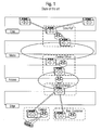
- Figure 1 shows an architecture of an optical network according to the state of the art.
- the network architecture is hierarchical having the highest data rates in an optical core network, such as a back-bone network of a country.
- an optical core network such as a back-bone network of a country.
- To each core network several optical metro networks can be connected, for instance in a ring structure.
- To each metro network in turn several access networks can be connected.
- the edge of the network as shown in figure 1 is formed by terminal devices T which can be connected via xDSL (version of Digital Subscriber Line) to a host device, for example to a switch in an DSLAM (Digital Subsciber Line Access Multiplexer).
- This switch is connected via an optical transport system (designated as FSP in all figures) and optical transport means to a transport system of a local exchange.
- FSP optical Transport System
- the core, metro and access network can have a ring structure, for example formed by two optical fibres and by transport systems.
- the optical fibres can transport data by means of wave length division multiplexing WDM.
- WDM wave length division multiplexing
- optical carrier signals are multiplexed on a single optical fibre by using different wave lengths ⁇ (colours) to carry different data signals. This allows an increased bandwidth and makes it possible to perform bidirectional communication over one strand of fibre.
- WDM-systems allow to expand the capacity of a network without laying more fibre.
- the capacity of an optical fibre can be expanded by upgrading multiplexers and demultiplexers at each end. This is often done by using optical-to-electrical-to-optical conversion at the edge of the transport network to permit interoperation with existing equipment.
- WDM-systems can be divided in different wave length patterns, i. e. conventional or coarse and dense WDM (CWDM, DWDM).
- CWDM coarse and dense WDM
- DWDM dense WDM
- GBIC Gigabit Interface Converter
- SFP Small Form Factor Pluggable
- an optical network can be formed by two main components, i. e. by a transport system and by host devices.
- Host devices include switching devices, such as routers, bridges, Ethernet switches, fibre channel switches or cross-connects.
- the network architecture as shown in figure 1 comprises optical interconnections, optical transport systems and host devices, such as switches or routers.
- the separation of functionality in two different device types of the conventional network as shown in figure 1 i. e. on the one hand transport of data (by the transport system) and on the other hand aggregation/switching data (by the host devices) increases complexity and costs.
- a small form factor pluggable is a compact optical transceiver using optical communication.
- a conventional small form factor pluggable module interfaces a network device mother board of a host device, such as a switch or router to an optical fibre or unshielded twisted pair networking cable.
- the SFP-transceivers are available in a variety of different transmitter and receiver types allowing users to select an appropriate transceiver for each link to provide a required optical reach over the available optical fibre type.
- a SFP-transceiver is specified by a multi-source agreement (MSA) between competing manufacturers.
- the SFP-module is designed after the GBIC-interface and allows greater data port density (i. e. number of transceivers per inch along the edge of a mother board) than GBIC.
- SFP-transceivers are commercially available and have a capability for data rates up to 4.25 Gbit/sec.
- a variant standard, XFP is capable of 10 Gbit/sec.
- SFP-transceivers support digital optical monitoring functions according to the industry standards SSF 8472 (ftp://ftp.seagate.com/sff/SFF-8472.PDF) multi-source agreement (MSA). This makes it possible for an end user to monitor real time parameters of the SFP-module, such as optical output power, optical input power, temperature, laser bias current and transceiver supply voltage.
- SSF 8472 ftp://ftp.seagate.com/sff/SFF-8472.PDF
- MSA multi-source agreement
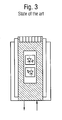
- FIGS 2 , 3 show a pluggable standard SFP-transceiver module according to the state of the art.
- the SFP pluggable module comprises an electrical interface connecting the pluggable module with a mother board of a host device by plugging the module into a cage of the host device board.
- On the front side of the pluggable module at least one optical fibre is attached to the module.
- FIG 4 shows a conventional system with pluggable SFP-transceivers according to the state of the art.
- a host device such as a switch or router, comprises a controller which is connected via a backplane to interface cards each having several cages which allow to plug in SFP-modules as shown in figure 3 .
- a transceiver within the pluggable module performs a conversion of the applied electrical signals to an optical signal which is forwarded via an optical fibre to the transport system.
- the transport system comprises several cards which comprise several cages for plug-in SFP-transceiver modules. These interface cards allow a switching, i. e. multiplexing or demultiplexing of signals within the electrical domain in response to control signals generated by a controller of the transport system and received via an internal management connection.
- the switched or controlled signals are applied to further modules for optical signals or optical fibres.
- These modules can, for example comprise variable optical attenuators (VOA), multiplexers/demultiplexers, amplifiers, switchers etc.
- VOA variable optical attenuators
- the signals are forwarded via optical fibres to remote far end transport systems over a distance of many kilometers, wherein the remote transport systems are in turn connected to far end host devices.
- Another disadvantage of a conventional system resides in that it does not allow a scalable connection of application ports of host devices. Furthermore, in a conventional system there is no flexibility with respect of different bandwidths of communication protocols used in the optical and electrical domain.
- the invention provides a network comprising at least one host device having an interface card connected to a backplane of a host device, wherein the interface card comprises at least one cage for receiving a pluggable module which provides an add-drop-functionality between an optical network interface and an electrical host interface.
- each pluggable module comprises an integrated bandwidth adaption unit.
- the bandwidth adaption unit provides an homogeneous distribution of an available protocol bandwidth to each host device of said network.
- said optical network interface comprises at least two bidirectional optical interface ports each performing single fibre working to provide bidirectional east and west communication within said network.
- the pluggable module performs a traffic management of data transported via an optical fibre connected to the pluggable module.
- the invention provides a pluggable module for bidirectional transport of data via at least one optical fibre between host devices, wherein said module is adapted to be pluggable into a corresponding cage of one of said host devices to perform a traffic management of the transported data.
- the traffic management is performed within the pluggable module in an electrical domain or an optical domain.
- the pluggable module is formed by a SFP-module or a XFP module.
- the traffic management comprises near end and far end management of the transported data.
- the traffic management is based on a communication between the pluggable module and host devices.
- the traffic management is based on a communication between the pluggable module and host devices, wherein the communication is using a SFF 8742-programming page structure with no adaptions.
- the traffic management is based on a communication between the pluggable module and host devices, wherein the communication is using a SFF 8742-programming page structure with no adaptions and a time division multiplex update procedure to buffer additional near end or far end parameters within the provided SFF 8472-programming page structure.
- the traffic management is based on a communication between the pluggable module and host devices, wherein the communication is using a SFF 8742-programming page structure with additional address space.
- the traffic management is based on a communication between the pluggable module and a far end pluggable module.
- the host devices comprise switching devices and optical transport devices.
- the switching devices comprise routers, switches, Ethernet switches and fibre channel switches.
- the optical transport devices comprise SDH, SONET, PDH, OTH, Ethernet, Fibre Channel, FICON and uncompressed video transport devices.
- the pluggable module comprises an embedded communication channel (ECC) for exchanging management data, administrative data and performance monitoring data between said pluggable module and a far end pluggable module.
- ECC embedded communication channel
- the embedded communication channel ECC is implemented at a physical layer.
- the embedded communication channel ECC is provided by a side band modulation of a data signal of said transported data.
- the data signal is pulse amplitude modulated.
- the embedded communication channel ECC is implemented at a protocol layer.
- the embedded communication channel ECC uses a bandwidth not occupied by a transport protocol for exchanging data between the pluggable module and the far end pluggable module.
- the embedded communication channel ECC is provided by amplitude shift keying ASK or frequency shift keying FSK or phase shift keying PSK.
- the embedded communication channel ECC is implemented on a proprietary overhead that is generated on top of a transport protocol.
- the embedded communication channel ECC is implemented based on an overhead of a transport protocol.
- the embedded communication channel ECC is implemented in a frame structure of a protocol.
- the embedded communication ECC is implemented within a protocol layer.
- the pluggable module comprises a diagnostic unit which receives local performance data from electronic components of the pluggable module.
- the electronic components comprise a transmission diode, a receiving diode, a laser driver LD, a transimpedance amplifier TIA and a limiting or linear amplifier.
- the diagnostic unit comprises an electrical interface with said host device for reporting performance data.
- the electrical interface comprises an I 2 C bus.
- the diagnostic unit comprises a memory for storing local performance data of the pluggable module.
- the pluggable module comprises a mapping unit which controls a laser driver depending on the local performance data received from the diagnostic unit to transfer the performance data via the embedded communication channel ECC to the remote pluggable module.
- the pluggable module comprises a demapping unit for storing performance data extracted from the embedded communication channel ECC in a memory of the diagnostic unit.
- the performance data is extracted at a transimpedance amplifier TIA.
- the performance data comprises SFF 8472-performance parameters.
- the memory is a SFF 8472-memory comprising unallocated bytes used for exchanging DMI (digital monitoring interface)-performance data with a far end pluggable module.
- a second set of said SFF 8472-performance data which indicates a performance at the far end is stored.
- near end or far end digital performance parameters are stored in said memory.
- the DMI (digital monitoring interface)-performance data comprises a voltage, temperature and laser bias.
- the pluggable module performs near end and far end bidirectional performance monitoring.
- the pluggable module comprises at least one data processing circuit such as a FPGA for performing performance monitoring.
- the data processing circuit is connected to a diagnostic unit of the pluggable module.
- the data processing circuit increments at least one performance counter provided in a memory of the diagnostic unit depending on a measured performance indicator.
- the performance indicator is formed by a BER (bit error rate), a CV (code violation) or by frame drops.
- the memory of the diagnostic unit is a SFF 8472-memory comprising unallocated bytes used for a ES (error seconds) and a SES (severe error seconds) performance counter.
- said pluggable module comprises a SERDES (serial deserializer) for supplying data from a transmit data path to said data processing circuit, and a SERDES for supplying data from the reception data path of the pluggable module to said data processing circuit.
- SERDES serial deserializer
- the pluggable module performs a latency measurement of a latency for transporting data from the pluggable module to a remote far end pluggable module.
- the pluggable module performs a link test.
- the pluggable module performs a protocol mapping between two transport protocols.
- the protocol mapping comprises payload mapping.
- the protocol mapping comprises overhead mapping.
- the transport protocol comprises a OTH, Ethernet, SDH or Sonet data transport protocol.
- the protocol mapping is configurable.
- the transport protocols comprise OSI layer 1, OSI layer 2 and OSI layer 3 protocols.
- the pluggable module performs loop switching.
- the pluggable module provides time slots based or data packet based add-drop functionality between an optical network interface and an electrical host interface.
- the electrical host interface is a standard MSA-interface.
- a configuration of an add/drop protocol bandwidth within a standard protocol and an add/drop network element topology is configurable from the far end side.
- the pluggable module provides a management protocol between multiple pluggable modules that performs a network topology detection.
- the pluggable module provides a management protocol between multiple pluggable modules that perform automatic configuration of multiple pluggable modules that are connected to a common network based upon the topology information data and a set of default parameters.
- the management protocol and configuration capability provides an homogenous distribution of an available protocol bandwidth within the network of pluggable modules.
- the pluggable module comprises symmetric or asymmetric TDM (TDMA).
- TDMA symmetric or asymmetric TDM
- the pluggable module performs monitoring and manipulation of optical signals.
- the pluggable module comprises an optical filter.
- said pluggable module comprises a variable optical attenuator (VOA).
- VOA variable optical attenuator
- the pluggable module comprises an optical amplifier.
- the pluggable module comprises an optical switching device.
- the pluggable comprises a dispersion compensation unit.
- the pluggable module comprises an optical power splitter device.
- the pluggable module comprises an optical loop device.
- the pluggable module comprises an optical connection device.
- the invention further provides an interface card for a host device comprising at least one cage for receiving a pluggable module which provides an add-drop-functionality between an optical network interface and an electrical host interface.
- the invention further provides a host device comprising at least one interface card connected to a backplane of the host device, wherein said interface card comprises at least one cage for receiving a pluggable module which provides an add-drop-functionality between an optical network interface and an electrical host interface.
- the invention further provides a network comprising at least one host device having an interface card connected to a backplane of the host device, wherein the interface card comprises at least one cage for receiving a pluggable module which provides an add-drop-functionality between an optical network interface and an electrical host interface.
- the invention further provides a data transport system for transporting bidirectional optical data via at least one optical fibre, wherein at both ends of said optical fibre a pluggable module is attached which provides an add-drop-functionality between an optical network interface and an electrical host interface.
- the invention further provides a method for bidirectional transport of data between host devices of said network via at least one optical fibre, wherein a module attached to said optical fibre is connected to a corresponding cage of one of said host devices and an add-drop-functionality is provided by said pluggable module.
- the invention further provides a computer program comprising instructions for performing a method for bidirectional transport of data between host devices of a network via at least one optical fibre, wherein a module attached to said optical fibre is connected to a corresponding host device, wherein an add-drop-functionality is provided by the module under control of the computer program.
- the invention further provides a data carrier for storing a computer program comprising instructions for performing transport for bidirectional transport of data between host devices of the network via at least one optical fibre, wherein a module attached to the optical fibre is connected to a corresponding cage of one of the host devices, wherein an add-drop-functionality is provided by the module under control of the computer program.
- FIG. 5 shows a pluggable module 1 according to the present invention plugged into a cage of a host device 2.
- the host device 2 can be a switching device, such as a router, a bridge, an Ethernet bridge or a fibre channel switch.
- the module 1 as shown in figure 5 is adapted to be plugged into a corresponding cage of the host device 2 and can perform a traffic management of data which is transported bidirectionally via at least one optical fibre 3 between host devices 2 of a data network.
- Traffic management comprises the provision of an Embedded Communication Channel (ECC), reporting of DMI data via said Embedded Communication Channel, digital performance monitoring, Latency measurements, performing of link tests, protocol mapping time-slot based ADM, asymmetric TDM as well as optical signal processing.
- ECC Embedded Communication Channel
- the traffic management of the data is performed within the pluggable module 1 and can be either performed in the electrical domain or in the optical domain.
- the pluggable module 1 as shown in figure 5 comprises an SFP (small form factor) pluggable module and also supports digital monitoring functions according to SFF 8472.
- the pluggable module 1 according to the present invention does not only perform transceiver functions, i. e. conversion between the optical and electrical domain, but also data traffic management functions.
- the data traffic management is performed by the pluggable module 1 as a near end and far end traffic management of the transported data.
- the data traffic management is formed by a pluggable module 1 on the basis of the communication between the pluggable module 1 and different host devices 2 of the optical network.
- the communication is using a SFF 8742-programming page structure with no adaptions.
- the traffic management can be based on a communication between the pluggable module 1 and host devices 2, wherein the communication is using a SFF 8742-programming page structure with no adaptions and a time division multiplex update procedure to buffer additional near end or far end parameters within the provided SFF 8742-programming page structure.
- the traffic management can be based on a communication between the pluggable module 1 and host devices 2, wherein the communication is using a SFF 8742-programming page structure with additional address spaces.
- the traffic management can be based on a communication between the pluggable module 1 as shown in figure 5 and a far end pluggable module which is attached to a remote end of the optical fibre 3 as shown in figure 5 .
- the pluggable module 1 as shown in figure 5 comprises several transport management functionalities, such as protection switching, performance monitoring, OAM, DCN (Data Communication Network) , mapping and framing, amplification, reconfigurable optical add/drop multiplexing (ROADM) and dispersion compensation DC.
- Further traffic management functionalities can comprise an optical transmission impairment mitigation, such as amplification and chromatic polarization mode compensation.
- a traffic management functionality provided by a pluggable module 1 according to the present invention is electrical transmission and impairment mitigation with forward error correction and electronic dispersion compensation.
- a further traffic management functionality of the pluggable module 1 according to the present invention can be in one embodiment OAM (operation administration and maintenance) functionalities, such as performance monitoring, default management, inter-device communication, configuration management and security management.
- OAM operation administration and maintenance
- the pluggable module 1 comprises optical and/or electrical add/drop multiplexing functionalities. Furthermore, in a possible embodiment, the traffic management functionality of the pluggable module 1 comprises optical conversion with mapping and framing functions.
- the pluggable module 1 complies in a possible embodiment with existing MSA-agreements, such as SFP, SFP+, XFP, GBIC etc.
- FIG. 6 shows a possible embodiment of a host device 2 according to the present invention.
- the host device 2 comprises at least one interface card 4 connected to a common backplane 5 of the host device 2.
- Each interface card 4 comprises several cages 6 for receiving pluggable modules 1 according to the present invention.
- the interface card 4-1 comprises three cages 6A, 6B, 6C for receiving a corresponding SFP pluggable modules 1A, 1B, 1C.
- Each pluggable module 1 comprises on the front side an optical interface to at least one optical fibre 3.
- each SFP plug-in module 1 as shown in figure 6 comprises an interface with two optical fibres for bidirectional optical transport of data.
- each pluggable module 1 comprises at least an electrical interface for connecting the pluggable module 1 with the circuitry on the interface card 4 of the host device 2.
- Figure 7 shows an example for connecting host devices 2 of a network via pluggable modules 1 according to the present invention.
- a near end host device 2-1 can be connected via data transport systems to far end host devices 2-2, 2-3, 2-4.
- Each data transport system is provided for transporting bidirectional optical data via at least one optical fibre 3.
- a pluggable SFP-module 1 is attached and performs a traffic management of the transported data.
- FIG. 8 shows a possible embodiment of a data transport system for transporting bidirectional optical data according to the present invention.
- two pluggable modules 1A, 1B are attached via an optical interface to at least one optical fibre 3 connecting both modules.
- at least one of the pluggable modules 1A, 1B is capable of performing a data traffic management.
- both pluggable modules are formed by SFP-modules connected to each other via optical fibres 3.
- the network according to the present invention has the advantage when compared to the conventional system of figure 4 that a separate transport system device in a separate box is no longer necessary so that wiring host devices 2 within the network is much easier and more flexible. Since the separate transport system device is no longer necessary, the optical network using the pluggable modules 1 according to the present invention needs less space and is more transparent to users performing the wiring between the host devices 2.
- a further major advantage of the optical network using the pluggable modules 1 according to the present invention resides in that the number of domain conversions between the electrical and optical domain is minimized. For the transport of data from one host device 2 to another host device 2 only one conversion on the near end side and one conversion on the far end side has to be performed. In contrast, the conventional network as shown in figure 4 needs three domain conversions on each side.
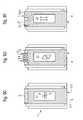
- FIGS 9A-9K show different embodiments of a pluggable module 1 according to the present invention.
- the pluggable module 1 comprises at least one optical interface 7 on the front side and an electrical interface 8 on the rear side.
- the electrical interface 8 comprises several electrical contacts for connecting the pluggable module 1 with the circuitry of a motherboard by inserting the pluggable module 1 into a corresponding cage 6 mounted on the mother board.
- the pluggable module 1 comprises an unidirectional single amplifier 9 within the pluggable module 1.
- the electrical interface 8 on the rear side of the pluggable module 1 can be formed by an I 2 C bus.
- the pluggable module 1 comprises a bidirectional signal amplifier 10, wherein each optical fibre 3-1, 3-2 transports data in both directions.
- the pluggable module 1 comprises a blocking filter 11 which can be either unidirectional or bidirectional.
- the blocking filter 11 can, for example block signals with different wavelength ⁇ with the exception of a predetermined wave length.
- Figure 9C shows a unidirectional blocking filter.
- Figure 9D shows a further embodiment of the pluggable module 1 according to the present invention.
- the pluggable module 1 comprises an OADM (Optical Add Drop Multiplexer) -filter 12 which is either unidirectional or bidirectional.
- Figure 9D shows an unidirectional OADM-filter 12.
- the pluggable module 1 has on the rear side not only an electrical interface 8 but also additional optical backplane plugs 13.
- the module 1 comprises four optical backplane plugs 13.
- the pluggable module 1 comprises six optical ports, i. e. four optical ports on the back side and two optical ports on the front side.
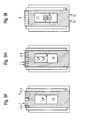
- Figure 9E shows a further embodiment of the pluggable module 1 according to the present invention.
- the pluggable module 1 comprises a connector plug 14, which can be either unidirectional or bidirectional.
- Figure 9E shows an unidirectional connector plug 14.
- the pluggable module 1 as shown in figure 9E connects the signals to the backplane of the host device 2 optically.
- the pluggable module 1 comprises optical backplane plugs 13-1, 13-2 as shown in figure 9E .
- Figure 9F shows a further embodiment of the pluggable module 1 according to the present invention.
- the pluggable module 1 comprises a loop plug 15.
- the loop plug 15 can be either unidirectional or bidirectional.
- Figure 9F shows a unidirectional loop plug.
- the pluggable module 1 does not comprise connectors on the front side.
- the loop plug 15 uses unused slots or connectors on the backside of the pluggable module 1.
- the loop can be either an electrical loop or an optical loop.
- two backplane optical plugs 13-1, 13-2 form an optical loop.
- FIGH shows a further embodiment of the pluggable module 1 according to the present invention.
- the pluggable module 1 comprises a double-loop plug 16 which loops unused slots on the back side of the pluggable module 1.
- no front connectors are provided.
- the embodiments as shown in figure 9F , 9A can be used for providing loops within a host device 2.
- Figure 9E shows a further embodiment of a pluggable module 1 according to the present invention.
- the pluggable module 1 comprises a dispersion compensation plug 17.
- the dispersion compensation plug 17 can be either unidirectional or bidirectional.
- Figure 9E shows a bidirectional dispersion compensation plug 17 within the pluggable module 1.
- the dispersion compensation unit DC can be, for example formed by a fibre bragg grating.
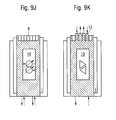
- FIG 9J shows a further embodiment of the pluggable module 1 according to the present invention.
- the pluggable module 1 is formed by a variable optical attenuator VOA 18.
- the variable optical attenuator 18 can be either unidirectional or bidirectional.
- Figure 9J shows a bidirectional variable optical attenuator 18.
- Figure 9K shows in a further embodiment of the pluggable module 1 according to the present invention.
- the pluggable module 1 comprises a power splitter 19.
- the power splitter 19 can be either unidirectional or bidirectional.
- Figure 9K shows a unidirectional power splitter.
- the pluggable module 1 comprises six ports, for example port 1 may have 100 %, port 5 x %, port 2 100 - x % of the power and port 3, 6, 4 may have an identical signal but with other direction.
- the host device 2 as shown in figure 6 may comprise in a possible embodiment an optical interface card 20 for several pluggable modules 1 according to the present invention as shown in figure 10 .
- different pluggable modules 1 are plugged into a corresponding cage 6 of the interface card 20 of a host device 2.
- the interface card 20 comprises in the given example nine cages 6-1 to 6-9 each provided for receiving a corresponding pluggable module 1.
- the pluggable modules 1-1, 1-2, 1-3, 1-5 and 1-6 are plugged into the corresponding cages 6 of the interface card 20.
- the pluggable module 1-1 comprises an unidirectional amplifier 9
- the second pluggable module 1-2 comprises a blocking filter 11
- the third pluggable module 1-3 is formed by a transceiver 21.
- the pluggable module 1-5 is also formed by a transceiver and the pluggable module 1-6 shown in figure 10 is formed by a variable optical attenuator VOA 18.
- the cages 6-4, 6-7, 6-8, 6-9 of the cartridge 20 are empty in the given example of figure 10 .
- Figure 11 shows a further example of a interface card 20 showing two wave lengths OADM.
- the first six cages 6-1 to 6-6 of the interface card 20 are occupied by plugged in pluggable modules 1-1 to 1-6.
- the first pluggable module 1-1 comprises a connector plug 14
- the second pluggable module 1-2 comprises a blocking filter 11
- the third pluggable module 1-3 comprises also a blocking filter 11
- the fourth pluggable module 1-4 comprises a connector plug 14
- the fifth pluggable module 1-5 is formed by a transceiver 21
- the sixth pluggable module 1-6 also comprises a transceiver 21.
- the pluggable module 1 comprises an embedded communication channel ECC as illustrated by figure 12 .
- the embedded communication channel ECC is provided between two pluggable modules 1A, 1B and is provided for exchanging management data, administrative data and performance monitoring data between the near end pluggable module 1A and a far end pluggable module 1 B.
- the embedded communication channel ECC is implemented at a physical layer.
- the embedded communication channel ECC can be provided by amplitude shift keying (ASK), frequency shift keying (FSK) or phase shift keying (PSK).
- ASK amplitude shift keying
- FSK frequency shift keying
- PSK phase shift keying
- the embedded communication channel ECC is provided by side band modulation of a data signal of transported data.
- the data signal is pulse amplitude modulated.
- the embedded communication channel ECC between the pluggable modules 1A, 1 B is implemented at a protocol layer.
- the embedded communication channel ECC uses a bandwidth not occupied by a transport protocol for exchanging data between the near end pluggable module 1A and a far end pluggable module 1 B.
- the embedded communication channel ECC is implemented on a proprietary overhead that is generated on top of a transport protocol.
- the embedded communication channel ECC can be implemented based on the overhead of a transport protocol, such as idle data patterns in inter-frame gaps.
- the embedded communication channel ECC can be implemented within a protocol layer, such as an Ethernet protocol.
- the embedded communication channel ECC can use existing protocol overheads or space in inter-frame gaps which can be implemented inside a protocol layer, such as EFM.
- mapping/demapping of data within the embedded communication channel ECC is performed within the pluggable module 1A, 1B.
- the purpose of the provided embedded communication channel ECC is to read performance monitoring data from the far end side, write PM-data to the far end side and to perform topology detection within the network of pluggable modules 1.
- the embedded communication channel ECC can be provided to read communication data from the far end side and to report to an internal controller of the near end pluggable module 1. With the embedded communication channel ECC it is further possible to write configuration data to the far end pluggable module controller and to allow communication between a near end host device 2A and a far end host device 2B as shown in figure 11 .
- ECC embedded communication channel
- DMI diagnostic parameters
- remote diagnostics parameters permanently available at a remote side, for example power local, power remote.
- SFF 8472 digital diagnostics I/F it is possible to latch remote data, i. e. store the data in a memory of the pluggable module 1.
- the embedded communication channel ECC There are two main possibilities for implementation of the embedded communication channel ECC.
- a physical layer implementation of the embedded communication channel ECC for example a pilot tone can be used.
- a slow AM modulation scheme (10 %, KHz range) available diagnostic I/F data can be imprinted on the embedded communication channel ECC.
- the embedded communication channel ECC can be implemented on a protocol layer.
- the embedded communication channel ECC can be provided on top of a service protocol.
- a high speed capable integrated circuit can be provided in a data path to imprint the embedded communication channel ECC. Imprinting of the embedded communication channel ECC can, for example use of inter-frame gaps for creation of an overhead OH.
- the available digital diagnostic I/F data can be imprinted or transferred on the embedded communication channel ECC.
- FIG. 13 shows a pluggable module 1 as employed within the network according to the present invention.
- the pluggable module 1 comprises an electrical host interface 8 connecting the pluggable network 1 with a host device 2.
- the pluggable module 1 is inserted into a cage 6 of the host device 2 and connected to the host device 2 via the electrical host interface 8 as shown in figure 13 .
- the cage 6 can be provided on an interface card 4 connected to a back plane 5 of the host device 2.
- the pluggable module 1 comprises an optical network interface 34.
- the optical interface 34 comprises in a preferred embodiment at least two bidirectional optical interface ports 34A, 34B which are shown in figure 13 . Each bidirectional optical interface port 34A, 34B performs single fibre working SFW to provide a bidirectional east and west communication within the network.
- each bidirectional optical interface port 34A, 34B an optical fibre 3A, 3B can be connected wherein each optical fibre 3A, 3B transports data in both directions.
- data can be transported to the bidirectional optical interface port 34A from a pluggable module of a remote host device via a first wavelength ( ⁇ 1A ) where as data from the interface port 34A is transferred to the remote pluggable module on a second wavelength ⁇ 2A as indicated in figure 13 .
- ⁇ 1A first wavelength
- ⁇ 2A second wavelength
- data is supplied from a second pluggable module of another far end host device to the bidirectional optical interface port 34B via a first wavelength ⁇ 1B and data is transferred in the other direction from the bidirectional optical interface port 34B to the second far and pluggable module by means of a second wavelength ⁇ 2B .
- the pluggable module 1 as shown in figure 13 comprises a diagnostic unit 22 to receive local performance data of electronic components within the pluggable module 1. These electronic components can form part of the bidirectional optical interface 34.
- the pluggable module 1 as shown in figure 13 further comprises an integrated bandwidth adaption unit 32.
- the pluggable module 1 according to the present invention comprises a diagnostic unit 22 to receive local performance data of electronic components.
- the pluggable module 1 as shown in figure 13 comprises an integrated bandwidth adaption unit 32.
- the integrated bandwidth adaption unit 32 is formed by an add/drop multiplexor ADM.
- the bandwidth adaption unit 32 provided a homogenous distribution of an available protocol bandwidth to each host device 2 of the network. As shown in fig.
- the bandwidth adaption unit 32 is connected to the electrical host interface 8 and to both bidirectional optical interface ports 34A, 34B of the optical interface 34.
- the bandwidth adaption unit 32 adapts the bandwidth of the data transport protocol as used by the host device 2 connected to the electrical host interface 8 to the bandwidth used in the optical domain by an optical data transport protocol.
- the physical bandwidth which can be used for transporting data with optical fibres 3A, 3B is identical, however a usable bandwidth of the two different bidirectional optical interface ports 34A, 34B can vary according the used data communication protocol.
- the physical bandwidth of the electrical host interface 8 as well as the usable bandwidth of the host device 2 can be different.
- the usable bandwidth for transporting data via the electrical host interface 8 depends on the data communication protocol provided by the host device 2.
- the usable bandwidth for transferring data is always smaller than the physical bandwidth provided by the data communication medium because a data communication protocol needs at least a part of the physical bandwidth for a exchanging control data.
- optical line data traffic may be 2x4 Gbit/sec (east and west) wherein the data traffic via the electrical host interface 8 can have a data traffic rate of 1x1 Gbit/sec.
- optical line data traffic may be 2x10 Gbit/sec (east and west) whereas the electrical host data traffic is 1x10 Gbit/sec.
- the optical line traffic might comprise 2x1 Gbit/sec (east and west) and the data rate via the electrical host interface 8 is "Zero" i. e. no data is exchanged via the electrical host interface 8.
- the optical line data traffic may comprise 2x1 Gbit/sec (east and west) and the electrical host data traffic has a physical data rate of 1x1 Gbit/sec with a net data rate of less than 1 Gbit/sec.
- the bandwidth adaption unit 32 of the pluggable module 1 is in a preferred embodiment programmable. In an alternative embodiment the bandwidth adaption unit 32 is hard wired.
- the bandwidth adaption unit 32 can be formed in a possible embodiment by a FPGA. In an alternative embodiment the bandwidth adaption unit 32 can be formed by an ASIC:
- the bandwidth adaption unit 32 can provide a symmetric or an asymmetric time slot based add/drop functionality between the optical network interface 34 and the electrical host interface 8.
- the bandwidth adaption unit 32 provides a data packet based add/drop functionality between the optical network interface 34 and the electrical host interface 8.
- a topology discovery is performed by a master host device 2-0 of the network using a topology discovery protocol for detecting a network topology of the network and in particular detecting the number of host devices 2 within the network.
- This topology discovery management protocol can comprise a LDP protocol or a TAD protocol.
- a master host device 2-0 can allocate the usable bandwidth to the remaining host devices 2 within the network depending on the topology using a bandwidth allocation management protocol such as RSVP-TE protocol. After the allocation of the bandwidth the bandwidth the bandwidth adaption units 32 of the network provides in a possible embodiment a homogenous distribution of the available protocol bandwidth to each host device 2 of the network.
- the physical bandwidth for transporting data in the optical domain is 1 Gbit/sec
- the usable bandwidth is 999 Mbit/sec
- the network comprises ten host devices 2 as detected during the network topology discovery
- each host device 2 of the network is allocated with a bandwidth of 99,9 MB/sec such providing a homogenous and fair distribution of the available protocol bandwidth to each host device 2 of the network.
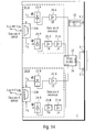
- FIG 14 shows a possible embodiment for the pluggable module 1 comprising an embedded communication channel ECC.
- the pluggable module 1 comprises a diagnostic unit 22 to receive local performance data of electronic components within the pluggable module 1. These electronic components comprise in the given example transmission diodes 23-A, 23-B, receiving diodes 24-A, 24-B, transimpedance amplifiers TIA 25-A, 25-B, laser drivers 26-A, 26-B and limiting or linear amplifiers 27-A, 27-B provided within the optical interface ports 34 A, 34 B.
- the electrical interface 8 comprises a data transmission interface 8-1, an electrical reporting interface 8-2 and for the reception data path an electrical data reception interface 8-3.
- the pluggable module 1 can comprise a mapping unit which controls the laser drivers 26 depending on local performance data received from the diagnostic unit 22 to transfer the performance data via an embedded communication channel ECC to a remote pluggable module 1.
- the pluggable module 1 can further comprise a demapping unit for storing performance data extracted from the embedded communication channel ECC in a memory of the diagnostic unit 22.
- the performance data can be extracted, for example at the transimpedance amplifiers 25 and the embedded communication channel ECC can be provided by side band modulation of a data signal of the transported data stream.
- the diagnostic unit 22 receives local performance data from the electronic components 23, 24, 25, 26, 27, such as temperature T or power consumption P.
- the diagnostic unit 22 reports the received local (near end) performance data and the received remote (far end) performance data transported via the embedded communication channel ECC via the electrical interface 8-2 to a controlling device of the host device 2 into which the pluggable module 1 is inserted.
- the electrical interface 8-2 can be formed in a possible embodiment by an I 2 C bus.
- the performance data extracted at the transimpedance amplifier TIA comprises SFF 8472-performance parameters.
- the diagnostic unit 22 comprises a memory for storing local performance data of the pluggable module 1 as well as the received and extracted performance data of remote pluggable modules.
- Figure 15 shows schematically a memory content of a memory 30 within the diagnostic unit 22 as shown in figure 13 .
- the memory 30 is a SSF 8472-memory having a page 30A and a page 30B.
- DMI digital monitoring interface
- This memory space can be used for transferring data from the diagnostic unit 22 to the respective host device 2.
- Figure 16 shows the memory space page 30B for storing real time diagnostic interface data in more detail.
- Data bytes 96-105 are used for local near end parameter data.
- data bytes 106-109 are unallocated data which can be used for transferring data via the embedded communication channel ECC to a far end pluggable module.
- the parameter data is refreshed in a fixed time period interval, such as every five seconds.
- the mapping and demapping units can be connected to a SFF 8472-diagnostic unit.
- the near end SSF 8472-data is read and written into the embedded communication channel ECC by such a mapping unit.
- the embedded communication channel ECC is read and the far end SFF 8472-parameter data is extracted and written to the near end SFF 8472-unit 22.
- the data is written to a diagnostic SSF 8472-unit 22 which supports SSF 8472 programming pages, so that address space extensions can be avoided to prevent adaptions of the hardware and software of the host device 2.
- a proprietary TDM-mapping scheme can be supported to map such data sets into the address space.
- the pluggable module 1 can perform near end and far end bidirectional performance monitoring.
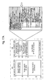
- Figures 17A , 17B show different possibilities to read out data using a memory 30 within the diagnostic unit 22.
- free memory space of the memory 30 as shown in figure 14 is used to read out data.
- an additional programming page 30C is provided to read out performance data.
- the memory 30 within the diagnostic unit 22 is a SFF 8472-memory comprising unallocated bytes used for an ES (error seconds), a SES (severe error seconds) a UAS (Unavailable Seconds) and a BER (Bit Error Rate) performance counter.
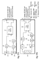
- Figure 18A illustrates a possibility of a line attenuation measurement which can be performed as performance monitoring by the pluggable module 1 according to the present invention.
- the communication is performed via a management channel inside of a frame.
- the controller 22B measures the laser output power in the given example.
- the FPGA 32B of the pluggable module 1 B sends the measured value of the controller 22B via a management frame channel to the other pluggable module 1A.
- the controller 22A of the pluggable module 1A measures an optical input power (OIP) and compares then the optical input power with the laser output power (LOP) from the other side.
- OIP optical input power
- LOP laser output power
- Figure 18B shows a further possible embodiment for measuring a line attenuation.
- a laser output power (LOP) is measured.
- the pluggable module 1 B sends the measured value of the laser output power (LOP) to the other pluggable module 1 A.
- the pluggable module 1A compares the received value with its optical input power so that the local FPGA 32A can analyze the attenuation of the link.
- the start value of attenuation (at the start-up of the line first time) can be compared with the current measurement value of attenuation.
- a communication is performed via a pilot tone.
- the communication is performed via a management channel inside a frame.
- FIGS 19 , 20 illustrate performance monitoring by a pluggable module 1 according to the present invention.
- the FPGA 32 is provided in the data path for monitoring the data path.
- the FPGA 32B detects with the help of SERDES various frame properties, such as running disparity, simple disparity, code error or a disparity error.
- Figure 21 illustrates a PRBS (Pseudo Random Bit Sequence) test.
- the line is analyzed by variation of a PRBS sequence, wherein two various operations can be provided.
- the FPGA 32B of pluggable module 1 B sends a PRBS-sequence to the FPGA 32A of the pluggable module 1A.
- the FPGA 32A of the pluggable module 1A loops the signal.
- the FPGA 32B of the pluggable module 1 B then receives its own PRBS-sequence and can analyze it and can calculate a line quality.
- Figure 22 illustrates a second operation variant for analyzing a line by variation of a PRBS-sequence.
- a separate PRBS-test is performed, i. e. a PRBS-test is performed for each separate line.
- the FPGA 32A of pluggable module 1A sends a PRBS-sequence to the FPGA 32B of the other pluggable module 1 B.
- the FPGA 32B of pluggable module 1 B analyzes the received PRBS-sequence.
- the same procedure is possible the other way around, i. e. the FPGA 32B of the pluggable module 1 B sends the PRBS-sequence to the FPGA 32A of the pluggable module 1A.
- FPGA 32B of pluggable module 1 B sends a special identifier to the FPGA 32A of the pluggable module 1 A.
- the FPGA 32A of the pluggable module 1A loops the received signal.
- the FPGA 32B of the second pluggable module 1 B receives the special identifier after a line delay time so that it can be analyzed and calculates the line length.
- the pluggable module 1 performs a latency measurement of a latency for transporting data from the pluggable module 1 to a far end pluggable module 1'.
- the measurement can be performed dynamically and without affecting data transmission.
- the near end pluggable module writes a byte x a time T1 into a signal overhead the far end pluggable module 1 extracts the byte X and writes it to an overhead byte Y at the far end transmitter.
- the near end pluggable module reads the received byte Y by extracting the T1-time stamp at the time T2.
- the latency T is written to the SFF 8472.
- the measurement procedure is performed symmetrically, i. e. latency T is available as a dynamical in-service measured parameter at the near end side and at the far end side.
- the measurement of the latency T is necessary to fulfil service level agreements (SLA).
- SLA service level agreements
- the latency T sometimes causes protocol buffering to manage protocol throughput, for example in a fibre channel protocol.
- the pluggable module 1 performs a link test.
- a link test is an initialization procedure that takes place before data transmission between host devices 2 is established.
- a received latency parameter at the far end pluggable module can be evaluated as a link test indication.
- the purpose of the link test is that it allows to set up and to verify an optical link between two pluggable modules 1 independently from the availability of host data.
- the pluggable module 1 performs a protocol mapping to transport protocols.
- the protocol mapping can comprise payload mapping or overhead mapping.
- the transport protocols comprise an OTH, Ethernet, SDH or Sonet data transport protocol.
- the protocol mapping performed by the pluggable module 1 is configurable.
- the transport protocols comprise OSI-layer 1, OSI-layer 2 and OSI-layer 3 protocols.
- the protocol mapping allows a bidirectional conversion between different types of protocols, such as Ethernet to SDH.
- the data traffic is mapped, i. e. payload mapping, OH-termination.
- a management mapping is performed, i. e. a data protocol conversion is performed.
- Figure 24 illustrates an example for protocol mapping as performed by the pluggable module 1.
- Figure 25 illustrates possible implementations of protocol mapping functions by the pluggable module 1 according to the present invention.
- the pluggable module 1 as shown in figure 13 , 14 provides an add/drop functionality between the optical network interface and an electrical host interface.
- the pluggable module 1 provides a single fibre working (SFW) on both interface ports 34 A, 34 B to provide bidirectional east/west communication with an optical network as illustrated by figures 13 , 14 .
- the add/drop multiplexing (ADM) functionality provided by the pluggable module 1 according to the present invention can be either proprietary or standard conform.
- the pluggable module 1 comprises an add/drop multiplexer ADM 32 which can be formed by a FPGA.
- the add drop multiplexer 32 is formed by an ASIC.
- ADM always needs east and west interfaces.
- Conventional pluggable modules offer only a bidirectional interface.
- the pluggable module 1 With the pluggable module 1 according to the present invention, single fibre working (SFW) is used inside the pluggable module 1 on the existing optical ports of the pluggable module 1.
- the pluggable module 1 comprises a multiplexer/demultiplexer 33A, 33B for the optical ports of the pluggable module 1.
- the couplers 33A, 33B are provided for bi-di selection, i. e. WWDM.
- the ADM-scheme can be configured either via the host devices 2 or independently from the host devices 2.
- the embedded communication channels ECC allows a host to host communication through the pluggable module 1.
- the host management interface allows to set up ADM-scheme parameters.
- the protocol of the embedded communication channel ECC allows to detect how many pluggable modules (M) share a common bandwidth (B). For fair bandwidth distribution, each pluggable module 1 effectively determines a fractional bandwidth B : M.
- the embedded communication channel ECC then automatically configures a set of M-pluggable modules 1 of a common network to a bandwidth B : M each.
- the ADM employed by the pluggable module 1 according to the present invention performs regeneration. When no bandwidth is terminated inside a node, only a passthrough is regenerated for transmission purposes.
- a further feature of the ADM as employed by the pluggable module 1 according to the present invention is protection, i. e. the ability to switch between a bandwidth termination from east and west side in case of a major event.
- the ADM-functionality of the pluggable module 1 according to the present invention allows to connect host devices 2 in a multiple node network to share a common optical fibre infrastructure.
- Figure 26A illustrates an add/drop from west or east as performed by the pluggable module 1 according to the present invention.
- Figure 26B illustrates a passthrough (regeneration) as performed by the pluggable module 1 according to the present invention.
- Figure 26C illustrates a drop and continue from west or east as employed by the pluggable module 1 according to the present invention.
- the east/west scenarios as shown in figures 27A and 27C can be provided with optional protection switching.
- the traffic switching granularity can be a complete data stream (1 GB/sec., 4 GB/sec., 10 GB/sec.) or fractions of the data stream, such as time slots or data packets.
- a connection in east/west direction based on MSA can be achieved by single fibre working (SFW), i. e. if the transmitting and receiving directions are on the same optical fibre with different wave lengths.
- SFW single fibre working
- FIGS 27A, 27B illustrate MSA-compatible optical transceiver with integrated asymmetric Time Division Multiplexing TDM (TDMA) as employed by the pluggable module 1 according to an embodiment of the present invention.
- the host interface can be formed by a standard IEEE 802.3 interface with reduced net bandwidth (GB Ethernet or fast Ethernet or Ethernet).
- the FPGA 32 can be provided within the data path.
- the transceiver network can be either GPON/EPON based or proprietary.
- the bandwidth/TDMA time slot configuration can be performed via an optional host.
- TDMA-schemes are well-known, the most important TDMA-schemes are EPON (Ethernet PON) and GPON (Gigabit PON). PON stands for Passive Optical Network.
- a passive optical network is a point-to-multipoint, fibre-to-the-premises network architecture used to enable a single optical fibre to serve multiple premises.
- a passive optical network consists of an optical line termination (OLT) at the service provider central office and a number of optical network units (ONU) at the near end user.
- OLT optical line termination
- ONU optical network units
- a PON configuration reduces the amount of fibre and central office equipment required compared to point-to-point architectures.
- the TDMA basically maps a continuous data stream into a sequence of transmission time intervals.
- a feature of the ADM-scheme as employed by the pluggable module 1 according to the present invention is the capability to configure the ADM-scheme.
- Fig. 28 shows an exemplary embodiment of a network according to the present invention.
- the shown embodiment of the network comprises N+1 host devices 2-0 to 2-N connected to each other via optical fibres 3 in a daisy chain.
- each host device 2-I comprises a cage for receiving a pluggable module 1-i according to the present invention.
- each host device 2 comprises a plurality of cages for receiving several pluggable modules 1 allowing a more complex wiring.
- the number of host devices N can be 16.
- the host device 2-0 forms a master device which performs a topology discovery of the network using a topology discovery protocol such as LDP or TAD and then allocating usable bandwidth to the other host devices 2-1 to 2-N of the network depending on the detected electrical topology of the network using a bandwidth allocation management protocol such as RSVP-TE.
- a topology discovery protocol such as LDP or TAD
- a bandwidth allocation management protocol such as RSVP-TE
- the master host device 2-0 can allocate time slots to the different host devices 2-1 - 2-N depended on the detecting topology and the usable bandwidth of the respective host devices 2-i.
- Each pluggable module 1 as used in the network as shown in figure 28 can comprise at least two active optical bidirectional interfaces or interface ports for an ost-west connection doubling the reception and transmitting capacity in each transceiver.
- An optical connection of the ost-west interfaces of the duplex connector based MSA is provided by using single fibre working SFW, i.e. data in transmitting and reception direction are transported by the same optical fibre on different wavelength 7.
- SFW single fibre working SFW
- An over-frame over the protocols is implemented and an add/drop functionality can be provided.
- An additional management protocol which allows an automatic network configuration and bandwidth allocation is provided.
- the pluggable module 1 with its at least two bidirectional optical interface ports 34A, 34B a scalable wiring of application ports is possible without the use of external transport devices.
- the employment of a pluggable module 1 according to the present invention allows a scalable adaptable bandwidth allocation without a modification of the host devices 2-i within the network.
- the configuration of the ADM-scheme is performed via host devices 2.
- An embedded communication channel ECC enables a host-to-host communication through the pluggable module 1.
- a host management interface allows to set up TDMA-scheme parameters.
- an embedded communication channel ECC protocol allows to detect how many pluggable modules (M) share a common upstream bandwidth (B). For fair bandwidth distribution each pluggable module 1 gets the allowance to send a fractional bandwidth of size B : M in an upstream direction. The ECC then automatically configures a set of M pluggable modules 1 in a common network to upstream bandwidth B : M each.
- the ADM-functionality of the pluggable module 1 according to the present invention allows to connect host devices 2 in a multiple node-star-network according to a so-called PON-structure that shares a common optical fibre infrastructure.
- the pluggable module 1 according to the present invention, with the TDMA-function allows to connect a plurality of devices over a PON-infrastructure for additional active data transport devices.
- the host device 2 can comprise a standard transceiver port.
- the host device 2 receives an Ethernet data stream with a data throughput which is a fraction of the complete Ethernet bandwidth.
- the configuration of the bandwidth is performed automatically within the TDMA.
- the configuration is performed by transferring configuration parameters.
- the pluggable module 1 performs in a possible embodiment an optical amplification or optical attenuation, optical test functions and an optical dispersion compensation. With this functionality it is possible to connect host devices 2 in an optical network comprising sophisticated optical functions like wavelength division multiplexing (WDM) over longer distances between termination nodes that require a power level and dispersion management.
- WDM wavelength division multiplexing
- the pluggable module 1 according to the present invention performs in an embodiment a monitoring and a manipulation of optical signals.
Landscapes
- Engineering & Computer Science (AREA)
- Computer Networks & Wireless Communication (AREA)
- Optical Communication System (AREA)
- Small-Scale Networks (AREA)
Abstract
Description
- The invention relates to a method and a network for bidirectional transport of data and in particular to a pluggable module for bidirectional transport of data via at least one optical fibre between host devices providing add-drop-functionality.
-
Figure 1 shows an architecture of an optical network according to the state of the art. The network architecture is hierarchical having the highest data rates in an optical core network, such as a back-bone network of a country. To each core network several optical metro networks can be connected, for instance in a ring structure. To each metro network in turn several access networks can be connected. The edge of the network as shown infigure 1 is formed by terminal devices T which can be connected via xDSL (version of Digital Subscriber Line) to a host device, for example to a switch in an DSLAM (Digital Subsciber Line Access Multiplexer). This switch is connected via an optical transport system (designated as FSP in all figures) and optical transport means to a transport system of a local exchange. The core, metro and access network can have a ring structure, for example formed by two optical fibres and by transport systems. The optical fibres can transport data by means of wave length division multiplexing WDM. In wave length division multiplexing WDM optical carrier signals are multiplexed on a single optical fibre by using different wave lengths λ (colours) to carry different data signals. This allows an increased bandwidth and makes it possible to perform bidirectional communication over one strand of fibre. WDM-systems allow to expand the capacity of a network without laying more fibre. The capacity of an optical fibre can be expanded by upgrading multiplexers and demultiplexers at each end. This is often done by using optical-to-electrical-to-optical conversion at the edge of the transport network to permit interoperation with existing equipment. WDM-systems can be divided in different wave length patterns, i. e. conventional or coarse and dense WDM (CWDM, DWDM). A recent development relating course WDM is the creation of GBIC (Gigabit Interface Converter) and Small Form Factor Pluggable (SFP) transceivers using standardized CWDM-wave lengths. - As can be seen from
figure 1 , an optical network can be formed by two main components, i. e. by a transport system and by host devices. Host devices include switching devices, such as routers, bridges, Ethernet switches, fibre channel switches or cross-connects. The network architecture as shown infigure 1 comprises optical interconnections, optical transport systems and host devices, such as switches or routers. The separation of functionality in two different device types of the conventional network as shown infigure 1 , i. e. on the one hand transport of data (by the transport system) and on the other hand aggregation/switching data (by the host devices) increases complexity and costs. - Accordingly, it has been proposed to shift functionality of the transport system, in particular the electrical-to-optical conversion, into the host device by using pluggable transceivers.
- A small form factor pluggable (SFP) is a compact optical transceiver using optical communication. A conventional small form factor pluggable module interfaces a network device mother board of a host device, such as a switch or router to an optical fibre or unshielded twisted pair networking cable. The SFP-transceivers are available in a variety of different transmitter and receiver types allowing users to select an appropriate transceiver for each link to provide a required optical reach over the available optical fibre type.
- A SFP-transceiver is specified by a multi-source agreement (MSA) between competing manufacturers. The SFP-module is designed after the GBIC-interface and allows greater data port density (i. e. number of transceivers per inch along the edge of a mother board) than GBIC. SFP-transceivers are commercially available and have a capability for data rates up to 4.25 Gbit/sec. A variant standard, XFP, is capable of 10 Gbit/sec.
- Some SFP-transceivers support digital optical monitoring functions according to the industry standards SSF 8472 (ftp://ftp.seagate.com/sff/SFF-8472.PDF) multi-source agreement (MSA). This makes it possible for an end user to monitor real time parameters of the SFP-module, such as optical output power, optical input power, temperature, laser bias current and transceiver supply voltage.
-
Figures 2 ,3 show a pluggable standard SFP-transceiver module according to the state of the art. The SFP pluggable module comprises an electrical interface connecting the pluggable module with a mother board of a host device by plugging the module into a cage of the host device board. On the front side of the pluggable module at least one optical fibre is attached to the module. -
Figure 4 shows a conventional system with pluggable SFP-transceivers according to the state of the art. A host device, such as a switch or router, comprises a controller which is connected via a backplane to interface cards each having several cages which allow to plug in SFP-modules as shown infigure 3 . A transceiver within the pluggable module performs a conversion of the applied electrical signals to an optical signal which is forwarded via an optical fibre to the transport system. The transport system comprises several cards which comprise several cages for plug-in SFP-transceiver modules. These interface cards allow a switching, i. e. multiplexing or demultiplexing of signals within the electrical domain in response to control signals generated by a controller of the transport system and received via an internal management connection. From the interface cards within the transport system the switched or controlled signals are applied to further modules for optical signals or optical fibres. These modules can, for example comprise variable optical attenuators (VOA), multiplexers/demultiplexers, amplifiers, switchers etc. From the transport system connected to the near end host device, the signals are forwarded via optical fibres to remote far end transport systems over a distance of many kilometers, wherein the remote transport systems are in turn connected to far end host devices. - One disadvantage of the conventional system as shown in
figure 4 is that the complexity of the system is quite high because three domain conversions on the near end side and on the far end side have to be performed. As can be seen fromfigure 4 , an electrical signal of the near end host device is converted within the pluggable SFP-transceivers plugged into the interface card of the host device to an optical signal and then retransformed from the optical domain to the electrical domain by a SFP-transceiver plugged into a cage of an interface card of the transport system. After an electrical switching is performed depending on the control signal supplied by the controller of the transport system, the electrical signal is again transformed from the electrical domain into an optical domain by another plugged in SFP-transceiver. Accordingly at the near end side, three domain conversions, i. e. an electrical-to-optical, an optical-to-electrical and an electrical-to-optical conversion are necessary. On the far end side, the three conversions are performed again resulting in a total of six domain conversions. Because of the necessary domain conversions, the technical complexity of the system is quite high. Since two different devices, i. e. a host device and a transport system have to be provided on each side management efforts, the occupied space and power consumption are increased. - Another disadvantage of a conventional system resides in that it does not allow a scalable connection of application ports of host devices. Furthermore, in a conventional system there is no flexibility with respect of different bandwidths of communication protocols used in the optical and electrical domain.
- Accordingly, it is an object of the present invention to provide a network and a method which offer flexibility with respect to communication protocol bandwidths.
- The invention provides a network comprising at least one host device having an interface card connected to a backplane of a host device, wherein the interface card comprises at least one cage for receiving a pluggable module which provides an add-drop-functionality between an optical network interface and an electrical host interface.
- In an embodiment of the network according to the present invention each pluggable module comprises an integrated bandwidth adaption unit.
- In an embodiment the bandwidth adaption unit provides an homogeneous distribution of an available protocol bandwidth to each host device of said network.
- In an embodiment of the network according to the present invention said optical network interface comprises at least two bidirectional optical interface ports each performing single fibre working to provide bidirectional east and west communication within said network.
- In the network according to the present invention, the pluggable module performs a traffic management of data transported via an optical fibre connected to the pluggable module.
- The invention provides a pluggable module for bidirectional transport of data via at least one optical fibre between host devices, wherein said module is adapted to be pluggable into a corresponding cage of one of said host devices to perform a traffic management of the transported data.
- In a possible embodiment, the traffic management is performed within the pluggable module in an electrical domain or an optical domain.
- In a possible embodiment, the pluggable module is formed by a SFP-module or a XFP module.
- In a possible embodiment of the pluggable module according to the present invention, the traffic management comprises near end and far end management of the transported data.
- In a possible embodiment of the pluggable module according to the present invention, the traffic management is based on a communication between the pluggable module and host devices.
- In a possible embodiment of the pluggable module according to the present invention, the traffic management is based on a communication between the pluggable module and host devices, wherein the communication is using a SFF 8742-programming page structure with no adaptions.
- In a possible embodiment of the pluggable module according to the present invention, the traffic management is based on a communication between the pluggable module and host devices, wherein the communication is using a SFF 8742-programming page structure with no adaptions and a time division multiplex update procedure to buffer additional near end or far end parameters within the provided SFF 8472-programming page structure.
- In a further embodiment of the pluggable module according to the present invention, the traffic management is based on a communication between the pluggable module and host devices, wherein the communication is using a SFF 8742-programming page structure with additional address space.
- In a possible embodiment of the pluggable module according to the present invention, the traffic management is based on a communication between the pluggable module and a far end pluggable module.
- In a possible embodiment of the pluggable module according to the present invention, the host devices comprise switching devices and optical transport devices.
- In a possible embodiment, the switching devices comprise routers, switches, Ethernet switches and fibre channel switches.
- In a possible embodiment, the optical transport devices comprise SDH, SONET, PDH, OTH, Ethernet, Fibre Channel, FICON and uncompressed video transport devices.
- In an embodiment of the pluggable module according to the present invention, the pluggable module comprises an embedded communication channel (ECC) for exchanging management data, administrative data and performance monitoring data between said pluggable module and a far end pluggable module.
- In a possible embodiment of the pluggable module according to the present invention, the embedded communication channel ECC is implemented at a physical layer.
- In a possible embodiment of the pluggable module according to the present invention, the embedded communication channel ECC is provided by a side band modulation of a data signal of said transported data.
- In a possible embodiment of the pluggable module according to the present invention, the data signal is pulse amplitude modulated.
- In an embodiment of the pluggable module according to the present invention, the embedded communication channel ECC is implemented at a protocol layer.
- In a possible embodiment of the pluggable module according to the present invention, the embedded communication channel ECC uses a bandwidth not occupied by a transport protocol for exchanging data between the pluggable module and the far end pluggable module.
- In a possible embodiment of the pluggable module according to the present invention, the embedded communication channel ECC is provided by amplitude shift keying ASK or frequency shift keying FSK or phase shift keying PSK.
- In a possible embodiment of the pluggable module according to the present invention, the embedded communication channel ECC is implemented on a proprietary overhead that is generated on top of a transport protocol.
- In a possible embodiment of the pluggable module according to the present invention, the embedded communication channel ECC is implemented based on an overhead of a transport protocol.
- In a possible embodiment of the pluggable module according to the present invention, the embedded communication channel ECC is implemented in a frame structure of a protocol.
- In a possible embodiment of the pluggable module according to the present invention, the embedded communication ECC is implemented within a protocol layer.
- In an embodiment of the pluggable module according to the present invention, the pluggable module comprises a diagnostic unit which receives local performance data from electronic components of the pluggable module.
- In an embodiment of the pluggable module according to the present invention, the electronic components comprise a transmission diode, a receiving diode, a laser driver LD, a transimpedance amplifier TIA and a limiting or linear amplifier.
- In an embodiment of the pluggable module according to the present invention, the diagnostic unit comprises an electrical interface with said host device for reporting performance data.
- In a possible embodiment of the pluggable module according to the present invention, the electrical interface comprises an I2C bus.
- In an embodiment of the pluggable module according to the present invention, the diagnostic unit comprises a memory for storing local performance data of the pluggable module.
- In an embodiment of the pluggable module according to the present invention, the pluggable module comprises a mapping unit which controls a laser driver depending on the local performance data received from the diagnostic unit to transfer the performance data via the embedded communication channel ECC to the remote pluggable module.
- In an embodiment of the pluggable module according to the present invention, the pluggable module comprises a demapping unit for storing performance data extracted from the embedded communication channel ECC in a memory of the diagnostic unit.
- In an embodiment of the pluggable module according to the present invention, the performance data is extracted at a transimpedance amplifier TIA.
- In an embodiment of the pluggable module according to the present invention, the performance data comprises SFF 8472-performance parameters.
- In an embodiment of the pluggable module according to the present invention, the memory is a SFF 8472-memory comprising unallocated bytes used for exchanging DMI (digital monitoring interface)-performance data with a far end pluggable module.
- In an embodiment of the pluggable module according to the present invention, a second set of said SFF 8472-performance data which indicates a performance at the far end is stored.
- In an embodiment of the pluggable module according to the present invention, near end or far end digital performance parameters are stored in said memory.
- In an embodiment of the pluggable module according to the present invention, the DMI (digital monitoring interface)-performance data comprises a voltage, temperature and laser bias.
- In a possible embodiment of the pluggable module according to the present invention, the pluggable module performs near end and far end bidirectional performance monitoring.
- In an embodiment of the pluggable module according to the present invention, the pluggable module comprises at least one data processing circuit such as a FPGA for performing performance monitoring.
- In an embodiment of the pluggable module according to the present invention, the data processing circuit is connected to a diagnostic unit of the pluggable module.
- In a possible embodiment of the pluggable module according to the present invention, the data processing circuit increments at least one performance counter provided in a memory of the diagnostic unit depending on a measured performance indicator.
- In an embodiment of the pluggable module according to the present invention, the performance indicator is formed by a BER (bit error rate), a CV (code violation) or by frame drops.
- In an embodiment of the pluggable module according to the present invention, the memory of the diagnostic unit is a SFF 8472-memory comprising unallocated bytes used for a ES (error seconds) and a SES (severe error seconds) performance counter.
- In an embodiment of the pluggable module according to the present invention, said pluggable module comprises a SERDES (serial deserializer) for supplying data from a transmit data path to said data processing circuit, and a SERDES for supplying data from the reception data path of the pluggable module to said data processing circuit.
- In an embodiment of the pluggable module according to the present invention, the pluggable module performs a latency measurement of a latency for transporting data from the pluggable module to a remote far end pluggable module.
- In an embodiment of the pluggable module according to the present invention, the pluggable module performs a link test.
- In an embodiment of the pluggable module according to the present invention, the pluggable module performs a protocol mapping between two transport protocols.
- In an embodiment of the pluggable module according to the present invention, the protocol mapping comprises payload mapping.
- In a further embodiment of the pluggable module according to the present invention, the protocol mapping comprises overhead mapping.
- In an embodiment of the pluggable module according to the present invention, the transport protocol comprises a OTH, Ethernet, SDH or Sonet data transport protocol.
- In an embodiment of the pluggable module according to the present invention, the protocol mapping is configurable.
- In an embodiment of the pluggable module according to the present invention, the transport protocols comprise
OSI layer 1,OSI layer 2 andOSI layer 3 protocols. - In an embodiment of the pluggable module according to the present invention, the pluggable module performs loop switching.
- In an embodiment of the pluggable module according to the present invention, the pluggable module provides time slots based or data packet based add-drop functionality between an optical network interface and an electrical host interface.
- In an embodiment of the pluggable module according to the present invention, the electrical host interface is a standard MSA-interface.
- In an embodiment of the pluggable module according to the present invention, a configuration of an add/drop protocol bandwidth within a standard protocol and an add/drop network element topology is configurable from the far end side.
- In an embodiment of the pluggable module according to the present invention, the pluggable module provides a management protocol between multiple pluggable modules that performs a network topology detection.
- In an embodiment of the pluggable module according to the present invention, the pluggable module provides a management protocol between multiple pluggable modules that perform automatic configuration of multiple pluggable modules that are connected to a common network based upon the topology information data and a set of default parameters.
- In an embodiment of the pluggable module according to the present invention, the management protocol and configuration capability provides an homogenous distribution of an available protocol bandwidth within the network of pluggable modules.
- In an embodiment of the pluggable module according to the present invention, the pluggable module comprises symmetric or asymmetric TDM (TDMA).
- In an embodiment of the pluggable module according to the present invention, the pluggable module performs monitoring and manipulation of optical signals.
- In an embodiment of the pluggable module according to the present invention, the pluggable module comprises an optical filter.
- In a further embodiment of the pluggable module according to the present invention, said pluggable module comprises a variable optical attenuator (VOA).
- In an embodiment of the pluggable module according to the present invention, the pluggable module comprises an optical amplifier.
- In an embodiment of the pluggable module according to the present invention, the pluggable module comprises an optical switching device.
- In an embodiment of the pluggable module according to the present invention, the pluggable comprises a dispersion compensation unit.
- In an embodiment of the pluggable module according to the present invention, the pluggable module comprises an optical power splitter device.
- In an embodiment of the pluggable module according to the present invention, the pluggable module comprises an optical loop device.
- In an embodiment of the pluggable module according to the present invention, the pluggable module comprises an optical connection device.
- The invention further provides an interface card for a host device comprising at least one cage for receiving a pluggable module which provides an add-drop-functionality between an optical network interface and an electrical host interface.
- The invention further provides a host device comprising at least one interface card connected to a backplane of the host device, wherein said interface card comprises at least one cage for receiving a pluggable module which provides an add-drop-functionality between an optical network interface and an electrical host interface.
- The invention further provides a network comprising at least one host device having an interface card connected to a backplane of the host device, wherein the interface card comprises at least one cage for receiving a pluggable module which provides an add-drop-functionality between an optical network interface and an electrical host interface.
- The invention further provides a data transport system for transporting bidirectional optical data via at least one optical fibre, wherein at both ends of said optical fibre a pluggable module is attached which provides an add-drop-functionality between an optical network interface and an electrical host interface.
- The invention further provides a method for bidirectional transport of data between host devices of said network via at least one optical fibre, wherein a module attached to said optical fibre is connected to a corresponding cage of one of said host devices and an add-drop-functionality is provided by said pluggable module.
- The invention further provides a computer program comprising instructions for performing a method for bidirectional transport of data between host devices of a network via at least one optical fibre, wherein a module attached to said optical fibre is connected to a corresponding host device, wherein an add-drop-functionality is provided by the module under control of the computer program.
- The invention further provides a data carrier for storing a computer program comprising instructions for performing transport for bidirectional transport of data between host devices of the network via at least one optical fibre, wherein a module attached to the optical fibre is connected to a corresponding cage of one of the host devices, wherein an add-drop-functionality is provided by the module under control of the computer program.
- In the following, preferred embodiments of the method and system according to the present invention are described with reference to the enclosed figures.
-
Figure 1 shows an architecture of a hierarchical network according to the state of the art; -
Figure 2 shows an arrangement of a host device and a transport system according to the state of the art; -
Figure 3 shows a conventional FSP-module with a transceiver according to the state of the art; -
Figure 4 shows an arrangement of a host device and a transport system according to the state of the art for illustrating the problem underlying the present invention; -
Figure 5 shows a block diagram of a host device with a plugged in pluggable module according to the present invention; -
Figure 6 shows a block diagram of a host device according to an embodiment of the present invention; -
Figure 7 shows an exemplary arrangement of host devices connected to each other by means of a data transport system according to a possible embodiment of the present invention; -
Figure 8 shows an embodiment of a transport data system according to an embodiment of the present invention; -
Figures 9A-9K show different embodiments of a pluggable module according to the present invention; -
Figure 10 shows an embodiment of an interface card as employed by a host device according to a possible embodiment of the present invention; -
Figure 11 shows an interface card of a host device with plugged in modules according to the present invention; -
Figure 12 shows a diagram for illustrating an embedded communication channel which is provided by a pluggable module according to an embodiment of the present invention; -
Figure 13 shows a block diagram of a possible embodiment of a pluggable module according to the present invention; -
Figure 14 shows a possible embodiment of a pluggable module according to the present invention in more detail; -
Figure 15 shows a data structure of a memory within a pluggable module according to a possible embodiment of the present invention; -
Figure 16 shows a section within the memory shown infigure 15 ; -
Figures 17A ,17B show examples of data structures of a memory within possible embodiments of the pluggable module according to the present invention; -
Figures 18A ,18B illustrate possibilities of line attenuation measurements performed by the pluggable module according to the present invention; -
Figures 19 ,20 illustrate a performance monitoring as performed by the pluggable module according to the present invention; -
Figure 21 illustrates a PRBS (Pseudo Random Bit Sequence) -test as performed by a pluggable module according to the present invention; -
Figure 22 shows a variant of a PRBS (Pseudo Random Bit Sequence) -test as performed by a pluggable module according to the present invention; -
Figure 23 shows a further embodiment of the pluggable module according to the present invention; -
Figure 24 illustrates an example for protocol mapping performed by the pluggable module according to the present invention; -
Figure 25 illustrates possible implementations of protocol mapping functions by a pluggable module according to the present invention; -
Figure 26 shows another embodiment of the pluggable module providing single fibre working according to the present invention; -
Figures 26A, 26B, 26C illustrate different functions by the pluggable module according to the present invention; -
Figures 27A, 27B illustrate further embodiments of a pluggable module according to the present invention; -
Figure 28 shows an exemplary embodiment of a network according to the present invention; -
Figure 5 shows apluggable module 1 according to the present invention plugged into a cage of ahost device 2. Thehost device 2 can be a switching device, such as a router, a bridge, an Ethernet bridge or a fibre channel switch. Themodule 1 as shown infigure 5 is adapted to be plugged into a corresponding cage of thehost device 2 and can perform a traffic management of data which is transported bidirectionally via at least oneoptical fibre 3 betweenhost devices 2 of a data network. Traffic management comprises the provision of an Embedded Communication Channel (ECC), reporting of DMI data via said Embedded Communication Channel, digital performance monitoring, Latency measurements, performing of link tests, protocol mapping time-slot based ADM, asymmetric TDM as well as optical signal processing. - The traffic management of the data is performed within the
pluggable module 1 and can be either performed in the electrical domain or in the optical domain. Thepluggable module 1 as shown infigure 5 comprises an SFP (small form factor) pluggable module and also supports digital monitoring functions according to SFF 8472. Thepluggable module 1 according to the present invention does not only perform transceiver functions, i. e. conversion between the optical and electrical domain, but also data traffic management functions. The data traffic management is performed by thepluggable module 1 as a near end and far end traffic management of the transported data. The data traffic management is formed by apluggable module 1 on the basis of the communication between thepluggable module 1 anddifferent host devices 2 of the optical network. In a possible embodiment, the communication is using a SFF 8742-programming page structure with no adaptions. In further embodiments, the traffic management can be based on a communication between thepluggable module 1 andhost devices 2, wherein the communication is using a SFF 8742-programming page structure with no adaptions and a time division multiplex update procedure to buffer additional near end or far end parameters within the provided SFF 8742-programming page structure. In an alternative embodiment, the traffic management can be based on a communication between thepluggable module 1 andhost devices 2, wherein the communication is using a SFF 8742-programming page structure with additional address spaces. The traffic management can be based on a communication between thepluggable module 1 as shown infigure 5 and a far end pluggable module which is attached to a remote end of theoptical fibre 3 as shown infigure 5 . Thepluggable module 1 as shown infigure 5 comprises several transport management functionalities, such as protection switching, performance monitoring, OAM, DCN (Data Communication Network) , mapping and framing, amplification, reconfigurable optical add/drop multiplexing (ROADM) and dispersion compensation DC. Further traffic management functionalities can comprise an optical transmission impairment mitigation, such as amplification and chromatic polarization mode compensation. - A traffic management functionality provided by a
pluggable module 1 according to the present invention is electrical transmission and impairment mitigation with forward error correction and electronic dispersion compensation. - A further traffic management functionality of the
pluggable module 1 according to the present invention can be in one embodiment OAM (operation administration and maintenance) functionalities, such as performance monitoring, default management, inter-device communication, configuration management and security management. - The
pluggable module 1 according to the present invention comprises optical and/or electrical add/drop multiplexing functionalities. Furthermore, in a possible embodiment, the traffic management functionality of thepluggable module 1 comprises optical conversion with mapping and framing functions. Thepluggable module 1 complies in a possible embodiment with existing MSA-agreements, such as SFP, SFP+, XFP, GBIC etc. -
Figure 6 shows a possible embodiment of ahost device 2 according to the present invention. Thehost device 2 comprises at least oneinterface card 4 connected to acommon backplane 5 of thehost device 2. Eachinterface card 4 comprisesseveral cages 6 for receivingpluggable modules 1 according to the present invention. In the given example offigure 6 , the interface card 4-1 comprises threecages SFP pluggable modules pluggable module 1 comprises on the front side an optical interface to at least oneoptical fibre 3. In the given example, each SFP plug-inmodule 1 as shown infigure 6 comprises an interface with two optical fibres for bidirectional optical transport of data. On the rear side, eachpluggable module 1 comprises at least an electrical interface for connecting thepluggable module 1 with the circuitry on theinterface card 4 of thehost device 2. -
Figure 7 shows an example for connectinghost devices 2 of a network viapluggable modules 1 according to the present invention. In the given example, a near end host device 2-1 can be connected via data transport systems to far end host devices 2-2, 2-3, 2-4. Each data transport system is provided for transporting bidirectional optical data via at least oneoptical fibre 3. At both ends of theoptical fibre 3, a pluggable SFP-module 1 is attached and performs a traffic management of the transported data. -
Figure 8 shows a possible embodiment of a data transport system for transporting bidirectional optical data according to the present invention. As shown infigure 8 , twopluggable modules optical fibre 3 connecting both modules. In a possible embodiment, at least one of thepluggable modules optical fibres 3. - As can be seen from
figure 7 , with the data transport system according to the present invention as shown infigure 8 , it is possible to connect a near end host device 2-1 to a far end host device. It is also possible to wire the near end host device 2-1, for example via an optical fibre 3-4 as shown infigure 7 . As can be seen fromfigure 7 , the network according to the present invention has the advantage when compared to the conventional system offigure 4 that a separate transport system device in a separate box is no longer necessary so thatwiring host devices 2 within the network is much easier and more flexible. Since the separate transport system device is no longer necessary, the optical network using thepluggable modules 1 according to the present invention needs less space and is more transparent to users performing the wiring between thehost devices 2. - A further major advantage of the optical network using the
pluggable modules 1 according to the present invention resides in that the number of domain conversions between the electrical and optical domain is minimized. For the transport of data from onehost device 2 to anotherhost device 2 only one conversion on the near end side and one conversion on the far end side has to be performed. In contrast, the conventional network as shown infigure 4 needs three domain conversions on each side. -
Figures 9A-9K show different embodiments of apluggable module 1 according to the present invention. Thepluggable module 1 comprises at least oneoptical interface 7 on the front side and anelectrical interface 8 on the rear side. Theelectrical interface 8 comprises several electrical contacts for connecting thepluggable module 1 with the circuitry of a motherboard by inserting thepluggable module 1 into acorresponding cage 6 mounted on the mother board. - In the embodiment as shown in
figure 9A , thepluggable module 1 comprises an unidirectionalsingle amplifier 9 within thepluggable module 1. - The
electrical interface 8 on the rear side of thepluggable module 1 can be formed by an I2C bus. On the front side of thepluggable module 1, there are attached two optical fibres 3-1, 3-2, one for receiving an optical signal and one for transmitting an optical signal. - In the embodiment as shown in
figure 9B thepluggable module 1 comprises abidirectional signal amplifier 10, wherein each optical fibre 3-1, 3-2 transports data in both directions. - In the embodiment as shown in
figure 9C thepluggable module 1 comprises a blockingfilter 11 which can be either unidirectional or bidirectional. The blockingfilter 11 can, for example block signals with different wavelength λ with the exception of a predetermined wave length.Figure 9C shows a unidirectional blocking filter. -
Figure 9D shows a further embodiment of thepluggable module 1 according to the present invention. In the embodiment offigure 9D thepluggable module 1 comprises an OADM (Optical Add Drop Multiplexer) -filter 12 which is either unidirectional or bidirectional.Figure 9D shows an unidirectional OADM-filter 12. As can be seen fromfigure 9D thepluggable module 1 has on the rear side not only anelectrical interface 8 but also additional optical backplane plugs 13. In the given example, themodule 1 comprises four optical backplane plugs 13. As can be seen fromfigure 9D thepluggable module 1 comprises six optical ports, i. e. four optical ports on the back side and two optical ports on the front side. -
Figure 9E shows a further embodiment of thepluggable module 1 according to the present invention. In the embodiment as shown infigure 9E thepluggable module 1 comprises aconnector plug 14, which can be either unidirectional or bidirectional.Figure 9E shows anunidirectional connector plug 14. Thepluggable module 1 as shown infigure 9E connects the signals to the backplane of thehost device 2 optically. To achieve this, thepluggable module 1 comprises optical backplane plugs 13-1, 13-2 as shown infigure 9E . -
Figure 9F shows a further embodiment of thepluggable module 1 according to the present invention. In this embodiment, thepluggable module 1 comprises aloop plug 15. The loop plug 15 can be either unidirectional or bidirectional.Figure 9F shows a unidirectional loop plug. In the given embodiment as shown infigure 9F thepluggable module 1 does not comprise connectors on the front side. The loop plug 15 uses unused slots or connectors on the backside of thepluggable module 1. The loop can be either an electrical loop or an optical loop. In the example offigure 9F two backplane optical plugs 13-1, 13-2 form an optical loop. -
Figure 9H shows a further embodiment of thepluggable module 1 according to the present invention. In the shown embodiment thepluggable module 1 comprises a double-loop plug 16 which loops unused slots on the back side of thepluggable module 1. In the embodiment as shown infigure 9F no front connectors are provided. The embodiments as shown infigure 9F ,9A can be used for providing loops within ahost device 2. -
Figure 9E shows a further embodiment of apluggable module 1 according to the present invention. In the shown embodiment, thepluggable module 1 comprises adispersion compensation plug 17. The dispersion compensation plug 17 can be either unidirectional or bidirectional.Figure 9E shows a bidirectional dispersion compensation plug 17 within thepluggable module 1. The dispersion compensation unit DC can be, for example formed by a fibre bragg grating. -
Figure 9J shows a further embodiment of thepluggable module 1 according to the present invention. In the embodiment as shown infigure 9J thepluggable module 1 is formed by a variableoptical attenuator VOA 18. The variableoptical attenuator 18 can be either unidirectional or bidirectional.Figure 9J shows a bidirectional variableoptical attenuator 18. -
Figure 9K shows in a further embodiment of thepluggable module 1 according to the present invention. In the shown embodiment thepluggable module 1 comprises a power splitter 19. The power splitter 19 can be either unidirectional or bidirectional.Figure 9K shows a unidirectional power splitter. In the given example offigure 9K thepluggable module 1 comprises six ports, forexample port 1 may have 100 %, port 5 x %,port 2 100 - x % of the power andport - The
host device 2 as shown infigure 6 may comprise in a possible embodiment anoptical interface card 20 for severalpluggable modules 1 according to the present invention as shown infigure 10 . In the given example offigure 10 , differentpluggable modules 1 are plugged into acorresponding cage 6 of theinterface card 20 of ahost device 2. Theinterface card 20 comprises in the given example nine cages 6-1 to 6-9 each provided for receiving a correspondingpluggable module 1. In the given example offigure 10 the pluggable modules 1-1, 1-2, 1-3, 1-5 and 1-6 are plugged into the correspondingcages 6 of theinterface card 20. In the given example the pluggable module 1-1 comprises anunidirectional amplifier 9, the second pluggable module 1-2 comprises a blockingfilter 11 and the third pluggable module 1-3 is formed by atransceiver 21. The pluggable module 1-5 is also formed by a transceiver and the pluggable module 1-6 shown infigure 10 is formed by a variableoptical attenuator VOA 18. The cages 6-4, 6-7, 6-8, 6-9 of thecartridge 20 are empty in the given example offigure 10 . -
Figure 11 shows a further example of ainterface card 20 showing two wave lengths OADM. In the given example the first six cages 6-1 to 6-6 of theinterface card 20 are occupied by plugged in pluggable modules 1-1 to 1-6. In the given example the first pluggable module 1-1 comprises aconnector plug 14, the second pluggable module 1-2 comprises a blockingfilter 11, the third pluggable module 1-3 comprises also a blockingfilter 11, the fourth pluggable module 1-4 comprises aconnector plug 14, the fifth pluggable module 1-5 is formed by atransceiver 21 and the sixth pluggable module 1-6 also comprises atransceiver 21. - In a preferred embodiment of the
pluggable module 1 according to the present invention, thepluggable module 1 comprises an embedded communication channel ECC as illustrated byfigure 12 . The embedded communication channel ECC is provided between twopluggable modules end pluggable module 1A and a far endpluggable module 1 B. In a possible embodiment the embedded communication channel ECC is implemented at a physical layer. The embedded communication channel ECC can be provided by amplitude shift keying (ASK), frequency shift keying (FSK) or phase shift keying (PSK). In a possible embodiment the embedded communication channel ECC is provided by side band modulation of a data signal of transported data. In a possible embodiment the data signal is pulse amplitude modulated. - In a further embodiment the embedded communication channel ECC between the
pluggable modules end pluggable module 1A and a far endpluggable module 1 B. - In a possible embodiment the embedded communication channel ECC is implemented on a proprietary overhead that is generated on top of a transport protocol.
- In a further embodiment the embedded communication channel ECC can be implemented based on the overhead of a transport protocol, such as idle data patterns in inter-frame gaps.
- In a further embodiment the embedded communication channel ECC can be implemented within a protocol layer, such as an Ethernet protocol. The embedded communication channel ECC can use existing protocol overheads or space in inter-frame gaps which can be implemented inside a protocol layer, such as EFM.
- The mapping/demapping of data within the embedded communication channel ECC is performed within the
pluggable module - The purpose of the provided embedded communication channel ECC is to read performance monitoring data from the far end side, write PM-data to the far end side and to perform topology detection within the network of
pluggable modules 1. The embedded communication channel ECC can be provided to read communication data from the far end side and to report to an internal controller of the near endpluggable module 1. With the embedded communication channel ECC it is further possible to write configuration data to the far end pluggable module controller and to allow communication between a nearend host device 2A and a farend host device 2B as shown infigure 11 . - The provision of an embedded communication channel ECC allows remote reporting of diagnostic parameters, such as DMI. Furthermore, it is possible to make remote diagnostics parameters permanently available at a remote side, for example power local, power remote. By using standard SFF 8472 digital diagnostics I/F, it is possible to latch remote data, i. e. store the data in a memory of the
pluggable module 1. - There are two main possibilities for implementation of the embedded communication channel ECC. In a physical layer implementation of the embedded communication channel ECC, for example a pilot tone can be used. By using, for example a slow AM modulation scheme (10 %, KHz range) available diagnostic I/F data can be imprinted on the embedded communication channel ECC.
- In an alternative embodiment, the embedded communication channel ECC can be implemented on a protocol layer. For example, the embedded communication channel ECC can be provided on top of a service protocol. In a possible embodiment, a high speed capable integrated circuit can be provided in a data path to imprint the embedded communication channel ECC. Imprinting of the embedded communication channel ECC can, for example use of inter-frame gaps for creation of an overhead OH. The available digital diagnostic I/F data can be imprinted or transferred on the embedded communication channel ECC.
-
Figure 13 shows apluggable module 1 as employed within the network according to the present invention. Thepluggable module 1 comprises anelectrical host interface 8 connecting thepluggable network 1 with ahost device 2. Thepluggable module 1 is inserted into acage 6 of thehost device 2 and connected to thehost device 2 via theelectrical host interface 8 as shown infigure 13 . Thecage 6 can be provided on aninterface card 4 connected to aback plane 5 of thehost device 2. On the front side thepluggable module 1 comprises anoptical network interface 34. Theoptical interface 34 comprises in a preferred embodiment at least two bidirectionaloptical interface ports figure 13 . Each bidirectionaloptical interface port figure 13 to each bidirectionaloptical interface port optical fibre optical fibre optical interface port 34A from a pluggable module of a remote host device via a first wavelength (λ1A) where as data from theinterface port 34A is transferred to the remote pluggable module on a second wavelength λ2A as indicated infigure 13 . The same applies to the secondbidirectional interface port 34B. In the shown example data is supplied from a second pluggable module of another far end host device to the bidirectionaloptical interface port 34B via a first wavelength λ1B and data is transferred in the other direction from the bidirectionaloptical interface port 34B to the second far and pluggable module by means of a second wavelength λ2B. - The
pluggable module 1 as shown infigure 13 comprises adiagnostic unit 22 to receive local performance data of electronic components within thepluggable module 1. These electronic components can form part of the bidirectionaloptical interface 34. Thepluggable module 1 as shown infigure 13 further comprises an integratedbandwidth adaption unit 32. In the embodiment shown infigure 13 thepluggable module 1 according to the present invention comprises adiagnostic unit 22 to receive local performance data of electronic components. Furthermore, thepluggable module 1 as shown infigure 13 comprises an integratedbandwidth adaption unit 32. The integratedbandwidth adaption unit 32 is formed by an add/drop multiplexor ADM. In a possible embodiment thebandwidth adaption unit 32 provided a homogenous distribution of an available protocol bandwidth to eachhost device 2 of the network. As shown infig. 13 thebandwidth adaption unit 32 is connected to theelectrical host interface 8 and to both bidirectionaloptical interface ports optical interface 34. Thebandwidth adaption unit 32 adapts the bandwidth of the data transport protocol as used by thehost device 2 connected to theelectrical host interface 8 to the bandwidth used in the optical domain by an optical data transport protocol. The physical bandwidth which can be used for transporting data withoptical fibres optical interface ports electrical host interface 8 as well as the usable bandwidth of thehost device 2 can be different. The usable bandwidth for transporting data via theelectrical host interface 8 depends on the data communication protocol provided by thehost device 2. The usable bandwidth for transferring data is always smaller than the physical bandwidth provided by the data communication medium because a data communication protocol needs at least a part of the physical bandwidth for a exchanging control data. - Different data traffic scenarios are possible. For example optical line data traffic may be 2x4 Gbit/sec (east and west) wherein the data traffic via the
electrical host interface 8 can have a data traffic rate of 1x1 Gbit/sec. - In another scenario the optical line data traffic may be 2x10 Gbit/sec (east and west) whereas the electrical host data traffic is 1x10 Gbit/sec.
- Is the pluggable module used for data regeneration, the optical line traffic might comprise 2x1 Gbit/sec (east and west) and the data rate via the
electrical host interface 8 is "Zero" i. e. no data is exchanged via theelectrical host interface 8. - In a further scenario the optical line data traffic may comprise 2x1 Gbit/sec (east and west) and the electrical host data traffic has a physical data rate of 1x1 Gbit/sec with a net data rate of less than 1 Gbit/sec.
- Accordingly, there are 5 different bandwidth to be considered providing different traffic scenarios, i.e. the physical bandwidth of the
optical fibre 3, the usable bandwidth of the firstoptical fibre 3A, usable bandwidth of the secondoptical fibre 3B, the physical bandwidth of theelectrical host interface 8 and the usable bandwidth of theelectrical host interface 8. The usable bandwidth depends on the employed data communication protocol and is always smaller than the corresponding physical bandwidth. Thebandwidth adaption unit 32 of thepluggable module 1 is in a preferred embodiment programmable. In an alternative embodiment thebandwidth adaption unit 32 is hard wired. Thebandwidth adaption unit 32 can be formed in a possible embodiment by a FPGA. In an alternative embodiment thebandwidth adaption unit 32 can be formed by an ASIC: - In a possible embodiment the
bandwidth adaption unit 32 can provide a symmetric or an asymmetric time slot based add/drop functionality between theoptical network interface 34 and theelectrical host interface 8. - In an alternative embodiment the
bandwidth adaption unit 32 provides a data packet based add/drop functionality between theoptical network interface 34 and theelectrical host interface 8. - In a possible embodiment a topology discovery is performed by a master host device 2-0 of the network using a topology discovery protocol for detecting a network topology of the network and in particular detecting the number of
host devices 2 within the network. This topology discovery management protocol can comprise a LDP protocol or a TAD protocol. After the topology of the network has been detected a master host device 2-0 can allocate the usable bandwidth to the remaininghost devices 2 within the network depending on the topology using a bandwidth allocation management protocol such as RSVP-TE protocol. After the allocation of the bandwidth thebandwidth adaption units 32 of the network provides in a possible embodiment a homogenous distribution of the available protocol bandwidth to eachhost device 2 of the network. For example if the physical bandwidth for transporting data in the optical domain is 1 Gbit/sec, the usable bandwidth is 999 Mbit/sec and the network comprises tenhost devices 2 as detected during the network topology discovery, eachhost device 2 of the network is allocated with a bandwidth of 99,9 MB/sec such providing a homogenous and fair distribution of the available protocol bandwidth to eachhost device 2 of the network. -
Figure 14 shows a possible embodiment for thepluggable module 1 comprising an embedded communication channel ECC. In the shown embodiment, thepluggable module 1 comprises adiagnostic unit 22 to receive local performance data of electronic components within thepluggable module 1. These electronic components comprise in the given example transmission diodes 23-A, 23-B, receiving diodes 24-A, 24-B, transimpedance amplifiers TIA 25-A, 25-B, laser drivers 26-A, 26-B and limiting or linear amplifiers 27-A, 27-B provided within theoptical interface ports pluggable module 1 theelectrical interface 8 comprises a data transmission interface 8-1, an electrical reporting interface 8-2 and for the reception data path an electrical data reception interface 8-3. Furthermore, thepluggable module 1 can comprise a mapping unit which controls thelaser drivers 26 depending on local performance data received from thediagnostic unit 22 to transfer the performance data via an embedded communication channel ECC to a remotepluggable module 1. Thepluggable module 1 can further comprise a demapping unit for storing performance data extracted from the embedded communication channel ECC in a memory of thediagnostic unit 22. The performance data can be extracted, for example at thetransimpedance amplifiers 25 and the embedded communication channel ECC can be provided by side band modulation of a data signal of the transported data stream. Thediagnostic unit 22 receives local performance data from theelectronic components diagnostic unit 22 reports the received local (near end) performance data and the received remote (far end) performance data transported via the embedded communication channel ECC via the electrical interface 8-2 to a controlling device of thehost device 2 into which thepluggable module 1 is inserted. The electrical interface 8-2 can be formed in a possible embodiment by an I2C bus. In a possible embodiment, the performance data extracted at the transimpedance amplifier TIA comprises SFF 8472-performance parameters. In a possible embodiment, thediagnostic unit 22 comprises a memory for storing local performance data of thepluggable module 1 as well as the received and extracted performance data of remote pluggable modules. -
Figure 15 shows schematically a memory content of amemory 30 within thediagnostic unit 22 as shown infigure 13 . In the shown embodiment, thememory 30 is a SSF 8472-memory having apage 30A and apage 30B. As can be seen fromfigure 14 , in the SSF 8472-memory unallocated bytes onpage 30B are used for exchanging DMI (digital monitoring interface) performance data with a far endpluggable module 1. This memory space can be used for transferring data from thediagnostic unit 22 to therespective host device 2. -
Figure 16 shows thememory space page 30B for storing real time diagnostic interface data in more detail. Data bytes 96-105 are used for local near end parameter data. As can be seen fromfigure 16 data bytes 106-109 are unallocated data which can be used for transferring data via the embedded communication channel ECC to a far end pluggable module. In a possible embodiment, the parameter data is refreshed in a fixed time period interval, such as every five seconds. - The mapping and demapping units can be connected to a SFF 8472-diagnostic unit. The near end SSF 8472-data is read and written into the embedded communication channel ECC by such a mapping unit. The embedded communication channel ECC is read and the far end SFF 8472-parameter data is extracted and written to the near end SFF 8472-
unit 22. The data is written to a diagnostic SSF 8472-unit 22 which supports SSF 8472 programming pages, so that address space extensions can be avoided to prevent adaptions of the hardware and software of thehost device 2. To meet space constraints within the SSF 8472-address space a proprietary TDM-mapping scheme can be supported to map such data sets into the address space. - In a possible embodiment of the
pluggable module 1 according to the present invention, thepluggable module 1 can perform near end and far end bidirectional performance monitoring. -
Figures 17A ,17B show different possibilities to read out data using amemory 30 within thediagnostic unit 22. In the embodiment as illustrated byfigure 17A , free memory space of thememory 30 as shown infigure 14 is used to read out data. - In the embodiment as illustrated in
figure 17B , anadditional programming page 30C is provided to read out performance data. - In a possible embodiment, the
memory 30 within thediagnostic unit 22 is a SFF 8472-memory comprising unallocated bytes used for an ES (error seconds), a SES (severe error seconds) a UAS (Unavailable Seconds) and a BER (Bit Error Rate) performance counter. -
Figure 18A illustrates a possibility of a line attenuation measurement which can be performed as performance monitoring by thepluggable module 1 according to the present invention. In the shown embodiment, the communication is performed via a management channel inside of a frame. First, thecontroller 22B measures the laser output power in the given example. Then theFPGA 32B of thepluggable module 1 B sends the measured value of thecontroller 22B via a management frame channel to the otherpluggable module 1A. In a further step, thecontroller 22A of thepluggable module 1A measures an optical input power (OIP) and compares then the optical input power with the laser output power (LOP) from the other side. -
Figure 18B shows a further possible embodiment for measuring a line attenuation. First, a laser output power (LOP) is measured. Then, thepluggable module 1 B sends the measured value of the laser output power (LOP) to the otherpluggable module 1 A. Thepluggable module 1A compares the received value with its optical input power so that thelocal FPGA 32A can analyze the attenuation of the link. For monitoring the line attenuation, the start value of attenuation (at the start-up of the line first time) can be compared with the current measurement value of attenuation. Now it is possible to calculate a line attenuation for a time and to monitor if sudden changes occur. In an embodiment, a communication is performed via a pilot tone. In an alternative embodiment, the communication is performed via a management channel inside a frame. -
Figures 19 ,20 illustrate performance monitoring by apluggable module 1 according to the present invention. TheFPGA 32 is provided in the data path for monitoring the data path. - The
FPGA 32B detects with the help of SERDES various frame properties, such as running disparity, simple disparity, code error or a disparity error. -
Figure 21 illustrates a PRBS (Pseudo Random Bit Sequence) test. In a possible embodiment, the line is analyzed by variation of a PRBS sequence, wherein two various operations can be provided. In a PRBS-loop test as illustrated byfigure 21 , theFPGA 32B ofpluggable module 1 B sends a PRBS-sequence to theFPGA 32A of thepluggable module 1A. TheFPGA 32A of thepluggable module 1A loops the signal. TheFPGA 32B of thepluggable module 1 B then receives its own PRBS-sequence and can analyze it and can calculate a line quality. -
Figure 22 illustrates a second operation variant for analyzing a line by variation of a PRBS-sequence. In this variant, a separate PRBS-test is performed, i. e. a PRBS-test is performed for each separate line. TheFPGA 32A ofpluggable module 1A sends a PRBS-sequence to theFPGA 32B of the otherpluggable module 1 B. Then, theFPGA 32B ofpluggable module 1 B analyzes the received PRBS-sequence. The same procedure is possible the other way around, i. e. theFPGA 32B of thepluggable module 1 B sends the PRBS-sequence to theFPGA 32A of thepluggable module 1A. This is provided for measurements of a line delay (line length). In a line delayloop test FPGA 32B ofpluggable module 1 B sends a special identifier to theFPGA 32A of thepluggable module 1 A. TheFPGA 32A of thepluggable module 1A loops the received signal. Then, theFPGA 32B of the secondpluggable module 1 B receives the special identifier after a line delay time so that it can be analyzed and calculates the line length. - In a possible embodiment, the
pluggable module 1 performs a latency measurement of a latency for transporting data from thepluggable module 1 to a far end pluggable module 1'. The measurement can be performed dynamically and without affecting data transmission. In a possible embodiment, the near end pluggable module writes a byte x a time T1 into a signal overhead the far endpluggable module 1 extracts the byte X and writes it to an overhead byte Y at the far end transmitter. The near end pluggable module reads the received byte Y by extracting the T1-time stamp at the time T2. The total delay time is T2 - T1. Accordingly, the measured one way latency is T = 0,5 * (T2 - T1). - In a possible embodiment, the latency T is written to the SFF 8472. In an embodiment, the measurement procedure is performed symmetrically, i. e. latency T is available as a dynamical in-service measured parameter at the near end side and at the far end side.
- The measurement of the latency T is necessary to fulfil service level agreements (SLA). The latency T sometimes causes protocol buffering to manage protocol throughput, for example in a fibre channel protocol.
- In a further embodiment of the
pluggable module 1 according to the present invention, thepluggable module 1 performs a link test. A link test is an initialization procedure that takes place before data transmission betweenhost devices 2 is established. A received latency parameter at the far end pluggable module can be evaluated as a link test indication. The purpose of the link test is that it allows to set up and to verify an optical link between twopluggable modules 1 independently from the availability of host data. - In an embodiment of the
pluggable module 1 according to the present invention, thepluggable module 1 performs a protocol mapping to transport protocols. - The protocol mapping can comprise payload mapping or overhead mapping. The transport protocols comprise an OTH, Ethernet, SDH or Sonet data transport protocol. In a possible embodiment, the protocol mapping performed by the
pluggable module 1 is configurable. In a possible embodiment, the transport protocols comprise OSI-layer 1, OSI-layer 2 and OSI-layer 3 protocols. The protocol mapping allows a bidirectional conversion between different types of protocols, such as Ethernet to SDH. - In a possible embodiment, the data traffic is mapped, i. e. payload mapping, OH-termination. In an alternative embodiment, a management mapping is performed, i. e. a data protocol conversion is performed.
-
Figure 24 illustrates an example for protocol mapping as performed by thepluggable module 1. -
Figure 25 illustrates possible implementations of protocol mapping functions by thepluggable module 1 according to the present invention. - In a possible embodiment of the
pluggable module 1 according to the present invention, thepluggable module 1 as shown infigure 13 ,14 provides an add/drop functionality between the optical network interface and an electrical host interface. - In a possible embodiment, the
pluggable module 1 provides a single fibre working (SFW) on bothinterface ports figures 13 ,14 . The add/drop multiplexing (ADM) functionality provided by thepluggable module 1 according to the present invention can be either proprietary or standard conform. In an embodiment thepluggable module 1 comprises an add/drop multiplexer ADM 32 which can be formed by a FPGA. In an alternative embodiment theadd drop multiplexer 32 is formed by an ASIC. ADM always needs east and west interfaces. Conventional pluggable modules offer only a bidirectional interface. With thepluggable module 1 according to the present invention, single fibre working (SFW) is used inside thepluggable module 1 on the existing optical ports of thepluggable module 1. As can be seen fromfigure 14 , thepluggable module 1 comprises a multiplexer/demultiplexer 33A, 33B for the optical ports of thepluggable module 1. Thecouplers - In a preferred embodiment with the ADM as employed by the
pluggable module 1 according to the present invention it is possible to configure the ADM-scheme. The configuration can be performed either via thehost devices 2 or independently from thehost devices 2. - The embedded communication channels ECC allows a host to host communication through the
pluggable module 1. The host management interface allows to set up ADM-scheme parameters. - If the configuration is performed independently from the
host devices 2, the protocol of the embedded communication channel ECC allows to detect how many pluggable modules (M) share a common bandwidth (B). For fair bandwidth distribution, eachpluggable module 1 effectively determines a fractional bandwidth B : M. The embedded communication channel ECC then automatically configures a set of M-pluggable modules 1 of a common network to a bandwidth B : M each. - In a possible embodiment, the ADM employed by the
pluggable module 1 according to the present invention performs regeneration. When no bandwidth is terminated inside a node, only a passthrough is regenerated for transmission purposes. A further feature of the ADM as employed by thepluggable module 1 according to the present invention, is protection, i. e. the ability to switch between a bandwidth termination from east and west side in case of a major event. The ADM-functionality of thepluggable module 1 according to the present invention allows to connecthost devices 2 in a multiple node network to share a common optical fibre infrastructure. -
Figure 26A illustrates an add/drop from west or east as performed by thepluggable module 1 according to the present invention. -
Figure 26B illustrates a passthrough (regeneration) as performed by thepluggable module 1 according to the present invention. -
Figure 26C illustrates a drop and continue from west or east as employed by thepluggable module 1 according to the present invention. - Those traffic switching functions can be realized within the
FPGA 32 of thepluggable module 1. The east/west scenarios as shown infigures 27A and 27C can be provided with optional protection switching. The traffic switching granularity can be a complete data stream (1 GB/sec., 4 GB/sec., 10 GB/sec.) or fractions of the data stream, such as time slots or data packets. A connection in east/west direction based on MSA can be achieved by single fibre working (SFW), i. e. if the transmitting and receiving directions are on the same optical fibre with different wave lengths. -
Figures 27A, 27B illustrate MSA-compatible optical transceiver with integrated asymmetric Time Division Multiplexing TDM (TDMA) as employed by thepluggable module 1 according to an embodiment of the present invention. The host interface can be formed by a standard IEEE 802.3 interface with reduced net bandwidth (GB Ethernet or fast Ethernet or Ethernet). TheFPGA 32 can be provided within the data path. The transceiver network can be either GPON/EPON based or proprietary. The bandwidth/TDMA time slot configuration can be performed via an optional host. TDMA-schemes are well-known, the most important TDMA-schemes are EPON (Ethernet PON) and GPON (Gigabit PON). PON stands for Passive Optical Network. A passive optical network is a point-to-multipoint, fibre-to-the-premises network architecture used to enable a single optical fibre to serve multiple premises. A passive optical network consists of an optical line termination (OLT) at the service provider central office and a number of optical network units (ONU) at the near end user. A PON configuration reduces the amount of fibre and central office equipment required compared to point-to-point architectures. - In order to keep MSA-compliance also on the
host interface side 8 of thepluggable module 1 and to avoid the need for host adaptions when supporting thepluggable module 1 according to the present invention, it is preferred to use a standard protocol. - Due to the nature of a TDM-scheme, upstream bandwidth compared to ONU is lower than the total bandwidth in the OLT-node. The TDMA basically maps a continuous data stream into a sequence of transmission time intervals.
- A feature of the ADM-scheme as employed by the
pluggable module 1 according to the present invention is the capability to configure the ADM-scheme. -
Fig. 28 shows an exemplary embodiment of a network according to the present invention. The shown embodiment of the network comprises N+1 host devices 2-0 to 2-N connected to each other viaoptical fibres 3 in a daisy chain. In the given example each host device 2-I comprises a cage for receiving a pluggable module 1-i according to the present invention. In other embodiments eachhost device 2 comprises a plurality of cages for receiving severalpluggable modules 1 allowing a more complex wiring. In a typical embodiment the number of host devices N can be 16. In the given example the host device 2-0 forms a master device which performs a topology discovery of the network using a topology discovery protocol such as LDP or TAD and then allocating usable bandwidth to the other host devices 2-1 to 2-N of the network depending on the detected electrical topology of the network using a bandwidth allocation management protocol such as RSVP-TE. For example the master host device 2-0 can allocate time slots to the different host devices 2-1 - 2-N depended on the detecting topology and the usable bandwidth of the respective host devices 2-i. - Each
pluggable module 1 as used in the network as shown infigure 28 , can comprise at least two active optical bidirectional interfaces or interface ports for an ost-west connection doubling the reception and transmitting capacity in each transceiver. An optical connection of the ost-west interfaces of the duplex connector based MSA is provided by using single fibre working SFW, i.e. data in transmitting and reception direction are transported by the same optical fibre ondifferent wavelength 7. By implementing a flexible FPGA an over-frame over the protocols is implemented and an add/drop functionality can be provided. An additional management protocol which allows an automatic network configuration and bandwidth allocation is provided. By using thepluggable module 1 with its at least two bidirectionaloptical interface ports pluggable module 1 according to the present invention allows a scalable adaptable bandwidth allocation without a modification of the host devices 2-i within the network. - In an embodiment of the
pluggable module 1, the configuration of the ADM-scheme is performed viahost devices 2. An embedded communication channel ECC enables a host-to-host communication through thepluggable module 1. A host management interface allows to set up TDMA-scheme parameters. - In an alternative embodiment, the configuration is performed independently from the
host devices 2. In a further embodiment, an embedded communication channel ECC protocol allows to detect how many pluggable modules (M) share a common upstream bandwidth (B). For fair bandwidth distribution eachpluggable module 1 gets the allowance to send a fractional bandwidth of size B : M in an upstream direction. The ECC then automatically configures a set of Mpluggable modules 1 in a common network to upstream bandwidth B : M each. - The ADM-functionality of the
pluggable module 1 according to the present invention allows to connecthost devices 2 in a multiple node-star-network according to a so-called PON-structure that shares a common optical fibre infrastructure. Thepluggable module 1 according to the present invention, with the TDMA-function allows to connect a plurality of devices over a PON-infrastructure for additional active data transport devices. Thehost device 2 can comprise a standard transceiver port. Thehost device 2 receives an Ethernet data stream with a data throughput which is a fraction of the complete Ethernet bandwidth. In a possible embodiment, the configuration of the bandwidth is performed automatically within the TDMA. In an alternative embodiment, the configuration is performed by transferring configuration parameters. - The
pluggable module 1 according to the present invention performs in a possible embodiment an optical amplification or optical attenuation, optical test functions and an optical dispersion compensation. With this functionality it is possible to connecthost devices 2 in an optical network comprising sophisticated optical functions like wavelength division multiplexing (WDM) over longer distances between termination nodes that require a power level and dispersion management. Thepluggable module 1 according to the present invention performs in an embodiment a monitoring and a manipulation of optical signals.
Claims (21)
- A network comprising at least one host device (2) having an interface card (4) connected to a backplane (5) of said host device (2),
wherein said interface card (4) comprises at least one cage (6) for receiving a pluggable module (1) which provides an add-drop-functionality between an optical network interface (34) and an electrical host interface (8). - The network according to claim 1,
wherein each pluggable module (1) comprises an integrated bandwidth adaption unit (32). - The network according to claim 2,
wherein said bandwidth adaption unit (32) provides a homogeneous distribution of an available protocol bandwidth to each host device (2) of said network. - The network according to claim 3,
wherein said optical network interface (34) comprises at least two bidirectional optical interface ports (34A, 34B) each performing a simple fibre working (SFW) to provide bidirectional east and west communication within said network. - The network according to claim 2,
wherein said bandwidth adaption unit (32) provides a symmetric or an asymmetric timeslot based add-drop-functionality between said optical network interface (34) and the electrical host interface (8). - The network according to claim 1,
wherein said bandwidth adaption unit (32) provides a data packet based add-drop-functionality between said optical network interface (34) and the electrical host interface (8). - The network according to claim 1,
wherein the electrical host interface (8) is a standard MSA interface. - The network according to claims 1-7,
wherein host devices (2) of said network are connected to each other by means of pluggable modules (1) in a daisy chain. - The network according to claims 1-8,
wherein a topology discovery performed by a master host device (2-0) of said network using a topology discovery protocol for detecting a network topology of said network. - The network according to claim 9,
wherein the number of host devices (2-i) of said network is detected by the topology discovery. - The network according to claims 9, 10,
wherein said master host device (2-0) allocates usable bandwidth to the other host devices (2-i) of said network depending on the electrical topology of the network using a bandwidth allocation management protocol. - The network according to claim 1,
wherein a configuration of an add/drop protocol bandwidth within a standard protocol and an add/drop network element topology is configurable from the far end side. - The network according to claim 1,
wherein said pluggable module (1) is adapted to configure an add/drop protocol bandwidth within a standard protocol and an add/drop network element topology from a far end pluggable module. - The network according to claim 9,
wherein said pluggable module (1) provides a management protocol between multiple pluggable modules that performs said network topology discovery. - The network according to claim 14,
wherein said pluggable module (1) further provides a management protocol between multiple pluggable modules that performs an automatic configuration of multiple pluggable modules(1) that are connected to said common network based upon topology information data and a set of default parameters. - A pluggable module (1) for bidirectional transport of data via at least one optical fibre (3) between host devices (2),
wherein said module (1) is adapted to be pluggable into a corresponding cage (6) of one of said host devices (2) and provides an add-drop-functionality between an optical network interface (34) and an electrical host interface (8). - The pluggable module (1) according to claim 16,
wherein said pluggable module (1) comprises:at least two bidirectional optical interface ports (34A, 34B) each performing single fibre working (SFW) to provide bidirectional East and West communication within a network and an integrated bandwidth adaption unit (32) provides an homogeneous distribution of available protocol bandwidth to each host device (2) of said network. - An interface card (4) for a host device (2) comprising at least one cage (6) for receiving a pluggable module (1) according to claims 16, 17.
- A host device (2) comprising at least one interface card (4) according to claim 18 connected to a backplane (5) of said host device (2).
- A data transport system for transporting bidirectional optical data via at least one optical fibre (3), wherein at both ends of said optical fibre (3) a pluggable module (1) according to claim 16 is attached which provides an add-drop-functionality between an optical network interface (34) and an electrical host interface (8).
- A method for bidirectional transport of data between host devices (2) of a network via at least one optical fibre (3),
wherein a pluggable module (1) attached to said optical fibre (3) is connected to a corresponding cage (6) of one of said host devices (2) and an add-drop functionality is provided by said pluggable module (1).
Priority Applications (1)
| Application Number | Priority Date | Filing Date | Title |
|---|---|---|---|
| EP08171052.7A EP2071861B1 (en) | 2007-12-12 | 2008-12-09 | A method and a network for bidirectional transport of data |
Applications Claiming Priority (3)
| Application Number | Priority Date | Filing Date | Title |
|---|---|---|---|
| EP07123047 | 2007-12-12 | ||
| EP20080156577 EP2124474B1 (en) | 2008-05-20 | 2008-05-20 | A data transport system with an embedded communication channel |
| EP08171052.7A EP2071861B1 (en) | 2007-12-12 | 2008-12-09 | A method and a network for bidirectional transport of data |
Publications (2)
| Publication Number | Publication Date |
|---|---|
| EP2071861A1 true EP2071861A1 (en) | 2009-06-17 |
| EP2071861B1 EP2071861B1 (en) | 2014-10-22 |
Family
ID=40405866
Family Applications (5)
| Application Number | Title | Priority Date | Filing Date |
|---|---|---|---|
| EP08171052.7A Active EP2071861B1 (en) | 2007-12-12 | 2008-12-09 | A method and a network for bidirectional transport of data |
| EP08171206.9A Active EP2071862B1 (en) | 2007-12-12 | 2008-12-10 | A method and a system for transporting of data with integrated protocol mapping function |
| EP08171352.1A Active EP2071863B1 (en) | 2007-12-12 | 2008-12-11 | A pluggable module with integrated data analysis function |
| EP08171376.0A Active EP2071864B1 (en) | 2007-12-12 | 2008-12-11 | A pluggable module with integrated time division multiplexing |
| EP08171513.8A Active EP2071865B1 (en) | 2007-12-12 | 2008-12-12 | A method and a network for processing of wavelength division multiplexed data |
Family Applications After (4)
| Application Number | Title | Priority Date | Filing Date |
|---|---|---|---|
| EP08171206.9A Active EP2071862B1 (en) | 2007-12-12 | 2008-12-10 | A method and a system for transporting of data with integrated protocol mapping function |
| EP08171352.1A Active EP2071863B1 (en) | 2007-12-12 | 2008-12-11 | A pluggable module with integrated data analysis function |
| EP08171376.0A Active EP2071864B1 (en) | 2007-12-12 | 2008-12-11 | A pluggable module with integrated time division multiplexing |
| EP08171513.8A Active EP2071865B1 (en) | 2007-12-12 | 2008-12-12 | A method and a network for processing of wavelength division multiplexed data |
Country Status (2)
| Country | Link |
|---|---|
| US (7) | US8358934B2 (en) |
| EP (5) | EP2071861B1 (en) |
Cited By (2)
| Publication number | Priority date | Publication date | Assignee | Title |
|---|---|---|---|---|
| CN109525563A (en) * | 2018-10-31 | 2019-03-26 | 哈尔滨电工仪表研究所有限公司 | The analytic method of reading object attribute in 698.45 agreement of DL/T |
| CN114500650A (en) * | 2022-01-25 | 2022-05-13 | 瀚云科技有限公司 | A traffic data processing method, device, server and system |
Families Citing this family (79)
| Publication number | Priority date | Publication date | Assignee | Title |
|---|---|---|---|---|
| EP2071861B1 (en) * | 2007-12-12 | 2014-10-22 | ADVA Optical Networking SE | A method and a network for bidirectional transport of data |
| JP5245895B2 (en) * | 2009-02-17 | 2013-07-24 | 富士通株式会社 | Transmission apparatus and line quality evaluation method |
| US8769654B2 (en) * | 2009-06-23 | 2014-07-01 | Cisco Technology, Inc. | Counterfeit prevention strategy for pluggable modules |
| US8615168B2 (en) * | 2009-07-02 | 2013-12-24 | At&T Intellectual Property I, L.P. | PON ONU configured in the form of a gigabit interface converter (GBIC) |
| US20110078346A1 (en) * | 2009-09-28 | 2011-03-31 | O'connor Michael | Computer Networking Device and Method Thereof |
| US9407426B2 (en) * | 2009-11-12 | 2016-08-02 | Oe Solutions America, Inc. | Optical network interface, module and engine |
| US8989590B2 (en) * | 2010-01-22 | 2015-03-24 | Broadcom Corporation | Pluggable OLT in Ethernet passive optical networks |
| WO2011100848A1 (en) * | 2010-02-22 | 2011-08-25 | Gennum Corporation | Backchannel communication between host and interface module |
| US8166183B2 (en) * | 2010-03-05 | 2012-04-24 | Ciena Corporation | Method and system for fast virtual concatenation setup in a communication network |
| US8761598B2 (en) * | 2010-04-08 | 2014-06-24 | Broadcom Corporation | Method and system for adaptively setting a transmitter filter for a high speed serial link transmitter |
| US20110268443A1 (en) * | 2010-04-29 | 2011-11-03 | Pmc Sierra Ltd. | Interface for pluggable pon ont |
| US8620156B2 (en) * | 2010-09-21 | 2013-12-31 | Adva Optical Networking Se | Method and apparatus for performing an automatic power adjustment for an optical signal |
| US8442401B2 (en) * | 2011-02-08 | 2013-05-14 | Telefonaktiebolaget L M Ericsson (Publ) | Method and device for fiber access physical layer unbundling using multiple uplink cards |
| US8292670B2 (en) | 2011-02-28 | 2012-10-23 | Honeywell International Inc. | Cable interface device |
| US20120275501A1 (en) * | 2011-04-27 | 2012-11-01 | Sergiu Rotenstein | Pluggable synchronization clocks, networks, systems and methods related thereto |
| WO2012154958A1 (en) | 2011-05-10 | 2012-11-15 | Invensys Systems, Inc. | Multi-drop optical communication |
| US8606112B2 (en) | 2011-07-21 | 2013-12-10 | Cisco Technology, Inc. | Pluggable module with bi-directional host-module optical interface |
| US9094128B2 (en) | 2011-08-11 | 2015-07-28 | Optoelectronics Solutions Co., Ltd. | Scheme for remote control of the output power of a transmitter in a smart SFP transceiver |
| US9485026B2 (en) * | 2011-09-16 | 2016-11-01 | OE Solutions Co., Ltd. | Scheme for remote control of the wavelength of a tunable transmitter in a smart transceiver |
| CA2855340A1 (en) * | 2011-11-09 | 2013-05-16 | Aurora Networks, Inc. | Adaptive equalization of impedance mismatched card-edge connections |
| EP2597801B1 (en) * | 2011-11-25 | 2014-01-08 | ADVA Optical Networking SE | Meshed protected passive optical access network structure and optical network unit structure therefore |
| US9438503B2 (en) * | 2012-03-05 | 2016-09-06 | Viavi Solutions Inc. | Network services testing with pluggable transceivers |
| US8989591B2 (en) | 2012-06-06 | 2015-03-24 | Techsys Insights | Remote optical demarcation point |
| US9014558B2 (en) * | 2012-06-06 | 2015-04-21 | Techsys Insights | Client grooming interface |
| US10012563B1 (en) * | 2012-07-18 | 2018-07-03 | Alliance Fiber Optic Products, Inc. | Polarity test of fiber arrays based on electronically switched optical signals |
| US9397754B2 (en) * | 2012-07-25 | 2016-07-19 | Finisar Corporation | Linecards with pluggable interfaces for pluggable optical amplifiers and other pluggable devices |
| WO2014047359A1 (en) * | 2012-09-19 | 2014-03-27 | Jds Uniphase Corporation | Network services testing with pluggable transceivers |
| US9482819B2 (en) * | 2013-03-04 | 2016-11-01 | Alliance Fiber Optic Products, Inc. | WDM Mux/DeMux on cable and methods of making the same |
| US20140270753A1 (en) * | 2013-03-13 | 2014-09-18 | Tellabs Operations, Inc. | Method and system for communicating with remote equipment |
| US9450854B2 (en) | 2013-03-14 | 2016-09-20 | Exfo Inc. | Pass-through test device |
| CN103326236B (en) * | 2013-06-19 | 2014-03-26 | 华中科技大学 | Semiconductor laser unit modulating and driving system |
| US9460049B2 (en) | 2013-07-18 | 2016-10-04 | Lenovo Enterprise Solutions (Singapore) Pte. Ltd. | Dynamic formation of symmetric multi-processor (SMP) domains |
| US9338528B2 (en) | 2013-07-18 | 2016-05-10 | Globalfoundries Inc. | Optimal positioning of reflecting optical devices |
| CN104969491B (en) * | 2013-12-20 | 2017-08-04 | 华为技术有限公司 | An optical module and system with adjustable bandwidth |
| GB2522469B (en) * | 2014-01-27 | 2017-10-11 | Nidec Control Techniques Ltd | Servo drive device |
| US9444827B2 (en) * | 2014-02-15 | 2016-09-13 | Micron Technology, Inc. | Multi-function, modular system for network security, secure communication, and malware protection |
| CA2942107C (en) | 2014-03-10 | 2021-01-05 | Aeponyx Inc. | Optical device with tunable optical wavelength selective circuit |
| US9497522B2 (en) * | 2014-08-19 | 2016-11-15 | Ciena Corporation | Flexible smart sleeve systems and methods for pluggable transceivers |
| US9769500B1 (en) * | 2014-12-11 | 2017-09-19 | Harmonic, Inc. | Smart small form-factor (SFP) pluggable transceiver |
| US20160261341A1 (en) * | 2015-02-26 | 2016-09-08 | Sifotonics Technologies Co., Ltd. | Monolithic Integrated Laser Driver And Limiting Amplifier With Micro-Programmed Controller And Flash Memory On SOC For Fiber Optical Transceiver |
| US9551831B1 (en) | 2015-05-18 | 2017-01-24 | Alliance Fiber Optic Products, Inc. | Pluggable LC adaptor having optical passive element |
| CN111061020B (en) * | 2015-06-15 | 2022-05-24 | 日本电气株式会社 | Pluggable Optical Modules and Optical Communication Systems |
| WO2016203683A1 (en) * | 2015-06-15 | 2016-12-22 | 日本電気株式会社 | Pluggable optical module and optical communication system |
| US10498451B2 (en) * | 2015-10-01 | 2019-12-03 | Hewlett Packard Enterprise Development Lp | Removable module |
| CN107438034A (en) * | 2016-05-25 | 2017-12-05 | 上海造瑞电子科技有限公司 | A kind of interchanger that can arbitrarily change transport media type |
| US9998213B2 (en) * | 2016-07-29 | 2018-06-12 | Keysight Technologies Singapore (Holdings) Pte. Ltd. | Network tap with battery-assisted and programmable failover |
| US10135538B2 (en) | 2016-08-02 | 2018-11-20 | Finisar Corporation | Signaling on a high-speed data connector |
| WO2018116516A1 (en) * | 2016-12-19 | 2018-06-28 | 日本電気株式会社 | Pluggable optical module and optical transmission system |
| US10419323B2 (en) * | 2017-04-24 | 2019-09-17 | Cisco Technology, Inc. | Modulation analyzer module |
| WO2019040438A1 (en) * | 2017-08-21 | 2019-02-28 | Menoher Jeffrey Charles | Hardware-enforced one-way information flow control device |
| US10998975B2 (en) * | 2017-08-21 | 2021-05-04 | Controlled Interfaces, LLC | Hardware-enforced one-way information flow control device |
| EP3462216B1 (en) * | 2017-09-27 | 2022-06-01 | Rockwell Automation Switzerland GmbH | Optoelectronic sensor having plug-in unit for providing extended functionality |
| US10277353B1 (en) | 2017-12-19 | 2019-04-30 | Juniper Networks, Inc. | Wavelength provisioning for customer premise equipment (CPE) in dense wavelength-division multiplex (DWDM) networks |
| JP7099088B2 (en) * | 2018-06-29 | 2022-07-12 | 日本電信電話株式会社 | Dispersion compensation system and dispersion compensation method |
| US10608774B2 (en) | 2018-07-27 | 2020-03-31 | At&T Intellectual Property I, L.P. | Network switch and optical transponder connectivity verification for wavelength division multiplexing network |
| US10491302B1 (en) | 2018-08-06 | 2019-11-26 | Hewlett Packard Enterprise Development Lp | Rack-level photonic solution |
| US10623101B1 (en) | 2018-08-07 | 2020-04-14 | Hewlett Packard Enterprise Development Lp | Hyperscale photonics connectivity solution |
| CN109537914B (en) * | 2018-11-30 | 2021-03-26 | 上海宝冶集团有限公司 | Synchronous operation control method for multi-group self-propelled module transport vehicle |
| US10757041B2 (en) | 2018-12-03 | 2020-08-25 | Hewlett Packard Enterprise Development Lp | Full server-level redundancy using a single network interface controller(NIC) and a single NIC card |
| WO2020195372A1 (en) * | 2019-03-26 | 2020-10-01 | 日本電気株式会社 | Light transmission device, and control method of same |
| CN110705232B (en) * | 2019-08-27 | 2023-04-07 | 国网山东省电力公司信息通信公司 | Method and system for generating service state analysis report of power communication network maintenance influence |
| CN111090526A (en) * | 2019-12-20 | 2020-05-01 | 北京浪潮数据技术有限公司 | Resource filtering method, device and related components |
| US11356754B2 (en) | 2020-03-08 | 2022-06-07 | Arista Networks, Inc. | Network device with integrated optical line system |
| US11144482B1 (en) | 2020-05-05 | 2021-10-12 | Micron Technology, Inc. | Bidirectional interface configuration for memory |
| CN111510800B (en) * | 2020-05-11 | 2021-12-10 | 安徽民生信息股份有限公司 | SDH transmission network safety monitoring system |
| US12029004B2 (en) | 2020-09-18 | 2024-07-02 | Nubis Communications, Inc. | Data processing systems including optical communication modules |
| EP4226195A4 (en) | 2020-10-07 | 2024-10-02 | Nubis Communications, Inc. | DATA PROCESSING SYSTEM WITH OPTICAL COMMUNICATION MODULES |
| WO2022109349A1 (en) | 2020-11-20 | 2022-05-27 | Nubis Communications, Inc. | Thermal design for rack mount systems including optical communication modules |
| CN112769474B (en) * | 2020-12-31 | 2022-02-11 | 中山大学 | A single-fiber bidirectional optical fiber transmission system based on asymmetric modulation spectrum |
| CN115118371A (en) * | 2021-03-18 | 2022-09-27 | 华为技术有限公司 | Method, device and system for processing Ethernet data in optical network |
| US12066653B2 (en) | 2021-04-22 | 2024-08-20 | Nubis Communications, Inc. | Communication systems having optical power supplies |
| US12461322B2 (en) | 2021-06-17 | 2025-11-04 | Nubis Communications, Inc. | Communication systems having pluggable modules |
| EP4356175A4 (en) | 2021-06-17 | 2025-07-16 | Nubis Communications Inc | COMMUNICATION SYSTEMS WITH PLUG-IN MODULES |
| EP4152065A1 (en) | 2021-09-16 | 2023-03-22 | Nubis Communications, Inc. | Communication systems having co-packaged optical modules |
| US12250024B2 (en) | 2021-09-16 | 2025-03-11 | Nubis Communications, Inc. | Data processing systems including optical communication modules |
| TW202345538A (en) * | 2022-01-11 | 2023-11-16 | 美商爾雅實驗室公司 | Systems and methods for remote optical power supply communication for uncooled wdm optical links |
| WO2023215315A1 (en) | 2022-05-02 | 2023-11-09 | Nubis Communications, Inc. | Communication systems having pluggable optical modules |
| US20240380489A1 (en) * | 2023-05-09 | 2024-11-14 | Apple Inc. | Configurable connector for optical bus |
| DE102024123785B4 (en) * | 2024-08-20 | 2026-03-05 | Deutsche Telekom Ag | Network transition facility |
Citations (1)
| Publication number | Priority date | Publication date | Assignee | Title |
|---|---|---|---|---|
| WO2003084281A1 (en) | 2002-03-28 | 2003-10-09 | Manifold Robert H | Optical communication management systems |
Family Cites Families (28)
| Publication number | Priority date | Publication date | Assignee | Title |
|---|---|---|---|---|
| US8412051B2 (en) * | 2006-10-13 | 2013-04-02 | Menara Networks, Inc. | 40G/100G optical transceivers with integrated framing and forward error correction |
| US7580637B2 (en) * | 2006-10-13 | 2009-08-25 | Menara Networks, Inc. | Systems and methods for the integration of framing, OAM and P, and forward error correction in pluggable optical transceiver devices |
| US8107820B2 (en) * | 2006-10-13 | 2012-01-31 | Menara Networks, Inc. | Systems and methods for the integration of framing, OAM&P, and forward error correction in SFP optical transceiver devices |
| US6665496B1 (en) * | 1998-04-27 | 2003-12-16 | Ciena Corporation | WDM ring transmission system |
| US20040252688A1 (en) * | 2001-08-28 | 2004-12-16 | May George Anthony | Routing packets in frame-based data communication networks |
| US7155133B2 (en) * | 2002-02-12 | 2006-12-26 | Finisar Corporation | Avalanche photodiode controller circuit for fiber optics transceiver |
| IL148994A (en) | 2002-04-04 | 2009-02-11 | Shai Amisar | Intravenous catheter assembly |
| US7941559B2 (en) * | 2002-04-23 | 2011-05-10 | Tellabs Bedford, Inc. | Media access control address translation for a fiber to the home system |
| US7304952B2 (en) | 2002-05-21 | 2007-12-04 | Applied Micro Circuits Corporation | Protocol-mapping network access device with user-provisionable wide area network flow control |
| US6893293B2 (en) | 2002-08-02 | 2005-05-17 | Finisar Corporation | Angled EMI shield for transceiver-PCB interface |
| US7447985B2 (en) * | 2002-08-15 | 2008-11-04 | Broadcom Corporation | Efficient design to implement min**/min**- or max**/max**- functions in LDPC (low density parity check) decoders |
| US7107414B2 (en) * | 2003-01-15 | 2006-09-12 | Avago Technologies Fiber Ip (Singapore) Ptd. Ltd. | EEPROM emulation in a transceiver |
| GB2405231B (en) * | 2003-08-20 | 2006-05-24 | Agilent Technologies Inc | Master slave arrangement |
| US7564798B2 (en) * | 2003-08-27 | 2009-07-21 | Finisar Corporation | Methods and devices for testing and monitoring high speed communication networks |
| US7518883B1 (en) * | 2003-10-09 | 2009-04-14 | Nortel Networks Limited | Backplane architecture for enabling configuration of multi-service network elements for use in a global variety of communications networks |
| US7433359B2 (en) | 2004-05-28 | 2008-10-07 | Fujitsu Limited | Application of an Ethernet/MPLS half bridge to provide Ethernet multiplexing functions (EMF) in SONET network elements (NEs) |
| US20050282413A1 (en) * | 2004-06-21 | 2005-12-22 | Israel Frederick S | Small form factor pluggable module providing passive optical signal processing of wavelength division multiplexed signals |
| US20060002710A1 (en) * | 2004-06-30 | 2006-01-05 | Finisar Corporation | Application-specific microcode for controlling an optical transceiver |
| US7672323B2 (en) * | 2005-01-14 | 2010-03-02 | Cisco Technology, Inc. | Dynamic and intelligent buffer management for SAN extension |
| US20060209886A1 (en) * | 2005-03-04 | 2006-09-21 | Rad Data Communications, Ltd. | Small form-factor device implementing protocol conversion |
| US20070086479A1 (en) * | 2005-09-30 | 2007-04-19 | Jing Ling | Techniques to buffer traffic in a communications system |
| US20070092257A1 (en) * | 2005-10-21 | 2007-04-26 | Smith Dale T | Optical interface for communicating optical transceiver status information |
| US8239919B2 (en) * | 2006-07-06 | 2012-08-07 | Mindspeed Technologies, Inc. | Flexible hardware password protection and access control |
| US8107821B2 (en) * | 2006-10-13 | 2012-01-31 | Menara Networks, Inc. | Systems and methods for Ethernet extension and demarcation |
| US7757936B2 (en) * | 2007-07-31 | 2010-07-20 | Hewlett-Packard Development Company, L.P. | System and method for cable monitoring |
| US20090116845A1 (en) * | 2007-11-02 | 2009-05-07 | Wen Li | Tetintelligent optical transceiver capable of optical-layer management |
| US20090240945A1 (en) * | 2007-11-02 | 2009-09-24 | Finisar Corporation | Anticounterfeiting means for optical communication components |
| EP2071861B1 (en) * | 2007-12-12 | 2014-10-22 | ADVA Optical Networking SE | A method and a network for bidirectional transport of data |
-
2008
- 2008-12-09 EP EP08171052.7A patent/EP2071861B1/en active Active
- 2008-12-10 EP EP08171206.9A patent/EP2071862B1/en active Active
- 2008-12-11 EP EP08171352.1A patent/EP2071863B1/en active Active
- 2008-12-11 US US12/332,919 patent/US8358934B2/en active Active
- 2008-12-11 EP EP08171376.0A patent/EP2071864B1/en active Active
- 2008-12-12 US US12/334,057 patent/US8644172B2/en active Active
- 2008-12-12 US US12/334,045 patent/US8300659B2/en active Active
- 2008-12-12 EP EP08171513.8A patent/EP2071865B1/en active Active
- 2008-12-12 US US12/334,026 patent/US8494362B2/en active Active
- 2008-12-12 US US12/334,076 patent/US8606103B2/en active Active
- 2008-12-12 US US12/333,928 patent/US8467679B2/en active Active
- 2008-12-12 US US12/334,053 patent/US8280249B2/en active Active
Patent Citations (1)
| Publication number | Priority date | Publication date | Assignee | Title |
|---|---|---|---|---|
| WO2003084281A1 (en) | 2002-03-28 | 2003-10-09 | Manifold Robert H | Optical communication management systems |
Non-Patent Citations (1)
| Title |
|---|
| OKAMOTO S ET AL: "IP BACKBONE NETWORK UTILIZING PHOTONIC TRANSPORT NETWORK TECHNOLOGIES", OPTICAL NETWORKS MAGAZINE, SPIE, BELLINGHAM, WA, US, vol. 1, no. 1, 1 January 2000 (2000-01-01), pages 19 - 28, XP000964318, ISSN: 1388-6916 * |
Cited By (2)
| Publication number | Priority date | Publication date | Assignee | Title |
|---|---|---|---|---|
| CN109525563A (en) * | 2018-10-31 | 2019-03-26 | 哈尔滨电工仪表研究所有限公司 | The analytic method of reading object attribute in 698.45 agreement of DL/T |
| CN114500650A (en) * | 2022-01-25 | 2022-05-13 | 瀚云科技有限公司 | A traffic data processing method, device, server and system |
Also Published As
| Publication number | Publication date |
|---|---|
| US20090154932A1 (en) | 2009-06-18 |
| US20090154918A1 (en) | 2009-06-18 |
| US8644172B2 (en) | 2014-02-04 |
| US8280249B2 (en) | 2012-10-02 |
| EP2071864B1 (en) | 2014-10-08 |
| EP2071865B1 (en) | 2014-04-16 |
| US8467679B2 (en) | 2013-06-18 |
| US20090162057A1 (en) | 2009-06-25 |
| US8606103B2 (en) | 2013-12-10 |
| US20090154930A1 (en) | 2009-06-18 |
| US8300659B2 (en) | 2012-10-30 |
| US20090169206A1 (en) | 2009-07-02 |
| EP2071861B1 (en) | 2014-10-22 |
| US20090161689A1 (en) | 2009-06-25 |
| EP2071864A1 (en) | 2009-06-17 |
| EP2071862B1 (en) | 2014-04-16 |
| EP2071863B1 (en) | 2014-04-16 |
| US8494362B2 (en) | 2013-07-23 |
| EP2071865A1 (en) | 2009-06-17 |
| US8358934B2 (en) | 2013-01-22 |
| EP2071863A1 (en) | 2009-06-17 |
| EP2071862A1 (en) | 2009-06-17 |
| US20090154493A1 (en) | 2009-06-18 |
Similar Documents
| Publication | Publication Date | Title |
|---|---|---|
| EP2071861B1 (en) | A method and a network for bidirectional transport of data | |
| JP4240602B2 (en) | Wavelength division multiplexed optical communication network with passive pass-through at each node | |
| US7747165B2 (en) | Network operating system with topology autodiscovery | |
| CN102413386A (en) | Passive optical network system, optical line terminator and communication method for passive optical network system | |
| EP2124474B1 (en) | A data transport system with an embedded communication channel | |
| CN112602273B (en) | Optical processing module and optical processing apparatus | |
| EP2071860B1 (en) | A method and a system for bidirectional transport of data | |
| US20090074412A1 (en) | Method, system, and computer program product for simulating an uplink through a network element | |
| Richter et al. | Field trial of an ASON in the metropolitan area | |
| KR100824146B1 (en) | WDM-POON transmission convergence device operating in multi-mode | |
| Jones et al. | Attributes of the Next Generation Sprint Optical Transport Network | |
| Yan et al. | Deliverable D3. 3 Evaluation of OPS, OCS and TOR switches' prototypes and programmable optical NICs including electronics control and interfaces | |
| Harney et al. | Optical Transport Network Management | |
| Kato et al. | Mitsubishi Electric | |
| CA2390586A1 (en) | Network operating system with topology autodiscovery |
Legal Events
| Date | Code | Title | Description |
|---|---|---|---|
| PUAI | Public reference made under article 153(3) epc to a published international application that has entered the european phase |
Free format text: ORIGINAL CODE: 0009012 |
|
| AK | Designated contracting states |
Kind code of ref document: A1 Designated state(s): AT BE BG CH CY CZ DE DK EE ES FI FR GB GR HR HU IE IS IT LI LT LU LV MC MT NL NO PL PT RO SE SI SK TR |
|
| AX | Request for extension of the european patent |
Extension state: AL BA MK RS |
|
| 17P | Request for examination filed |
Effective date: 20091217 |
|
| AKX | Designation fees paid |
Designated state(s): AT BE BG CH CY LI |
|
| RBV | Designated contracting states (corrected) |
Designated state(s): AT BE BG CH CY CZ DE DK EE ES FI FR GB GR HR HU IE IS IT LI LT LU LV MC MT NL NO PL PT RO SE SI SK TR |
|
| REG | Reference to a national code |
Ref country code: DE Ref legal event code: 8566 |
|
| 17Q | First examination report despatched |
Effective date: 20120220 |
|
| RAP1 | Party data changed (applicant data changed or rights of an application transferred) |
Owner name: ADVA OPTICAL NETWORKING SE |
|
| GRAP | Despatch of communication of intention to grant a patent |
Free format text: ORIGINAL CODE: EPIDOSNIGR1 |
|
| INTG | Intention to grant announced |
Effective date: 20140605 |
|
| GRAS | Grant fee paid |
Free format text: ORIGINAL CODE: EPIDOSNIGR3 |
|
| GRAA | (expected) grant |
Free format text: ORIGINAL CODE: 0009210 |
|
| AK | Designated contracting states |
Kind code of ref document: B1 Designated state(s): AT BE BG CH CY CZ DE DK EE ES FI FR GB GR HR HU IE IS IT LI LT LU LV MC MT NL NO PL PT RO SE SI SK TR |
|
| REG | Reference to a national code |
Ref country code: GB Ref legal event code: FG4D |
|
| REG | Reference to a national code |
Ref country code: CH Ref legal event code: EP |
|
| REG | Reference to a national code |
Ref country code: AT Ref legal event code: REF Ref document number: 693074 Country of ref document: AT Kind code of ref document: T Effective date: 20141115 |
|
| REG | Reference to a national code |
Ref country code: IE Ref legal event code: FG4D |
|
| REG | Reference to a national code |
Ref country code: DE Ref legal event code: R096 Ref document number: 602008034978 Country of ref document: DE Effective date: 20141218 |
|
| REG | Reference to a national code |
Ref country code: NL Ref legal event code: VDEP Effective date: 20141022 |
|
| REG | Reference to a national code |
Ref country code: AT Ref legal event code: MK05 Ref document number: 693074 Country of ref document: AT Kind code of ref document: T Effective date: 20141022 |
|
| REG | Reference to a national code |
Ref country code: LT Ref legal event code: MG4D |
|
| PG25 | Lapsed in a contracting state [announced via postgrant information from national office to epo] |
Ref country code: LT Free format text: LAPSE BECAUSE OF FAILURE TO SUBMIT A TRANSLATION OF THE DESCRIPTION OR TO PAY THE FEE WITHIN THE PRESCRIBED TIME-LIMIT Effective date: 20141022 Ref country code: NL Free format text: LAPSE BECAUSE OF FAILURE TO SUBMIT A TRANSLATION OF THE DESCRIPTION OR TO PAY THE FEE WITHIN THE PRESCRIBED TIME-LIMIT Effective date: 20141022 Ref country code: PT Free format text: LAPSE BECAUSE OF FAILURE TO SUBMIT A TRANSLATION OF THE DESCRIPTION OR TO PAY THE FEE WITHIN THE PRESCRIBED TIME-LIMIT Effective date: 20150223 Ref country code: NO Free format text: LAPSE BECAUSE OF FAILURE TO SUBMIT A TRANSLATION OF THE DESCRIPTION OR TO PAY THE FEE WITHIN THE PRESCRIBED TIME-LIMIT Effective date: 20150122 Ref country code: IS Free format text: LAPSE BECAUSE OF FAILURE TO SUBMIT A TRANSLATION OF THE DESCRIPTION OR TO PAY THE FEE WITHIN THE PRESCRIBED TIME-LIMIT Effective date: 20150222 Ref country code: FI Free format text: LAPSE BECAUSE OF FAILURE TO SUBMIT A TRANSLATION OF THE DESCRIPTION OR TO PAY THE FEE WITHIN THE PRESCRIBED TIME-LIMIT Effective date: 20141022 Ref country code: ES Free format text: LAPSE BECAUSE OF FAILURE TO SUBMIT A TRANSLATION OF THE DESCRIPTION OR TO PAY THE FEE WITHIN THE PRESCRIBED TIME-LIMIT Effective date: 20141022 |
|
| PG25 | Lapsed in a contracting state [announced via postgrant information from national office to epo] |
Ref country code: PL Free format text: LAPSE BECAUSE OF FAILURE TO SUBMIT A TRANSLATION OF THE DESCRIPTION OR TO PAY THE FEE WITHIN THE PRESCRIBED TIME-LIMIT Effective date: 20141022 Ref country code: LV Free format text: LAPSE BECAUSE OF FAILURE TO SUBMIT A TRANSLATION OF THE DESCRIPTION OR TO PAY THE FEE WITHIN THE PRESCRIBED TIME-LIMIT Effective date: 20141022 Ref country code: AT Free format text: LAPSE BECAUSE OF FAILURE TO SUBMIT A TRANSLATION OF THE DESCRIPTION OR TO PAY THE FEE WITHIN THE PRESCRIBED TIME-LIMIT Effective date: 20141022 Ref country code: HR Free format text: LAPSE BECAUSE OF FAILURE TO SUBMIT A TRANSLATION OF THE DESCRIPTION OR TO PAY THE FEE WITHIN THE PRESCRIBED TIME-LIMIT Effective date: 20141022 Ref country code: SE Free format text: LAPSE BECAUSE OF FAILURE TO SUBMIT A TRANSLATION OF THE DESCRIPTION OR TO PAY THE FEE WITHIN THE PRESCRIBED TIME-LIMIT Effective date: 20141022 Ref country code: GR Free format text: LAPSE BECAUSE OF FAILURE TO SUBMIT A TRANSLATION OF THE DESCRIPTION OR TO PAY THE FEE WITHIN THE PRESCRIBED TIME-LIMIT Effective date: 20150123 Ref country code: CY Free format text: LAPSE BECAUSE OF FAILURE TO SUBMIT A TRANSLATION OF THE DESCRIPTION OR TO PAY THE FEE WITHIN THE PRESCRIBED TIME-LIMIT Effective date: 20141022 |
|
| PG25 | Lapsed in a contracting state [announced via postgrant information from national office to epo] |
Ref country code: BE Free format text: LAPSE BECAUSE OF NON-PAYMENT OF DUE FEES Effective date: 20141231 |
|
| REG | Reference to a national code |
Ref country code: DE Ref legal event code: R097 Ref document number: 602008034978 Country of ref document: DE |
|
| PG25 | Lapsed in a contracting state [announced via postgrant information from national office to epo] |
Ref country code: EE Free format text: LAPSE BECAUSE OF FAILURE TO SUBMIT A TRANSLATION OF THE DESCRIPTION OR TO PAY THE FEE WITHIN THE PRESCRIBED TIME-LIMIT Effective date: 20141022 Ref country code: SK Free format text: LAPSE BECAUSE OF FAILURE TO SUBMIT A TRANSLATION OF THE DESCRIPTION OR TO PAY THE FEE WITHIN THE PRESCRIBED TIME-LIMIT Effective date: 20141022 Ref country code: DK Free format text: LAPSE BECAUSE OF FAILURE TO SUBMIT A TRANSLATION OF THE DESCRIPTION OR TO PAY THE FEE WITHIN THE PRESCRIBED TIME-LIMIT Effective date: 20141022 Ref country code: RO Free format text: LAPSE BECAUSE OF FAILURE TO SUBMIT A TRANSLATION OF THE DESCRIPTION OR TO PAY THE FEE WITHIN THE PRESCRIBED TIME-LIMIT Effective date: 20141022 Ref country code: LU Free format text: LAPSE BECAUSE OF FAILURE TO SUBMIT A TRANSLATION OF THE DESCRIPTION OR TO PAY THE FEE WITHIN THE PRESCRIBED TIME-LIMIT Effective date: 20141209 Ref country code: CZ Free format text: LAPSE BECAUSE OF FAILURE TO SUBMIT A TRANSLATION OF THE DESCRIPTION OR TO PAY THE FEE WITHIN THE PRESCRIBED TIME-LIMIT Effective date: 20141022 |
|
| REG | Reference to a national code |
Ref country code: CH Ref legal event code: PL |
|
| PLBE | No opposition filed within time limit |
Free format text: ORIGINAL CODE: 0009261 |
|
| STAA | Information on the status of an ep patent application or granted ep patent |
Free format text: STATUS: NO OPPOSITION FILED WITHIN TIME LIMIT |
|
| PG25 | Lapsed in a contracting state [announced via postgrant information from national office to epo] |
Ref country code: IT Free format text: LAPSE BECAUSE OF FAILURE TO SUBMIT A TRANSLATION OF THE DESCRIPTION OR TO PAY THE FEE WITHIN THE PRESCRIBED TIME-LIMIT Effective date: 20141022 |
|
| REG | Reference to a national code |
Ref country code: IE Ref legal event code: MM4A |
|
| REG | Reference to a national code |
Ref country code: FR Ref legal event code: ST Effective date: 20150831 |
|
| 26N | No opposition filed |
Effective date: 20150723 |
|
| PG25 | Lapsed in a contracting state [announced via postgrant information from national office to epo] |
Ref country code: LI Free format text: LAPSE BECAUSE OF NON-PAYMENT OF DUE FEES Effective date: 20141231 Ref country code: IE Free format text: LAPSE BECAUSE OF NON-PAYMENT OF DUE FEES Effective date: 20141209 Ref country code: CH Free format text: LAPSE BECAUSE OF NON-PAYMENT OF DUE FEES Effective date: 20141231 |
|
| PG25 | Lapsed in a contracting state [announced via postgrant information from national office to epo] |
Ref country code: FR Free format text: LAPSE BECAUSE OF NON-PAYMENT OF DUE FEES Effective date: 20141231 |
|
| PG25 | Lapsed in a contracting state [announced via postgrant information from national office to epo] |
Ref country code: SI Free format text: LAPSE BECAUSE OF FAILURE TO SUBMIT A TRANSLATION OF THE DESCRIPTION OR TO PAY THE FEE WITHIN THE PRESCRIBED TIME-LIMIT Effective date: 20141022 |
|
| PG25 | Lapsed in a contracting state [announced via postgrant information from national office to epo] |
Ref country code: MC Free format text: LAPSE BECAUSE OF FAILURE TO SUBMIT A TRANSLATION OF THE DESCRIPTION OR TO PAY THE FEE WITHIN THE PRESCRIBED TIME-LIMIT Effective date: 20141022 Ref country code: BG Free format text: LAPSE BECAUSE OF FAILURE TO SUBMIT A TRANSLATION OF THE DESCRIPTION OR TO PAY THE FEE WITHIN THE PRESCRIBED TIME-LIMIT Effective date: 20141022 |
|
| PG25 | Lapsed in a contracting state [announced via postgrant information from national office to epo] |
Ref country code: MT Free format text: LAPSE BECAUSE OF FAILURE TO SUBMIT A TRANSLATION OF THE DESCRIPTION OR TO PAY THE FEE WITHIN THE PRESCRIBED TIME-LIMIT Effective date: 20141022 Ref country code: TR Free format text: LAPSE BECAUSE OF FAILURE TO SUBMIT A TRANSLATION OF THE DESCRIPTION OR TO PAY THE FEE WITHIN THE PRESCRIBED TIME-LIMIT Effective date: 20141022 Ref country code: HU Free format text: LAPSE BECAUSE OF FAILURE TO SUBMIT A TRANSLATION OF THE DESCRIPTION OR TO PAY THE FEE WITHIN THE PRESCRIBED TIME-LIMIT; INVALID AB INITIO Effective date: 20081209 |
|
| P01 | Opt-out of the competence of the unified patent court (upc) registered |
Effective date: 20230630 |
|
| REG | Reference to a national code |
Ref country code: DE Ref legal event code: R081 Ref document number: 602008034978 Country of ref document: DE Owner name: ADTRAN NETWORKS SE, DE Free format text: FORMER OWNER: ADVA OPTICAL NETWORKING SE, 82152 PLANEGG, DE |
|
| PGFP | Annual fee paid to national office [announced via postgrant information from national office to epo] |
Ref country code: GB Payment date: 20251216 Year of fee payment: 18 |
|
| PGFP | Annual fee paid to national office [announced via postgrant information from national office to epo] |
Ref country code: DE Payment date: 20251222 Year of fee payment: 18 |