EP2071416A1 - Imaging unit and image forming apparatus using same - Google Patents
Imaging unit and image forming apparatus using same Download PDFInfo
- Publication number
- EP2071416A1 EP2071416A1 EP08171330A EP08171330A EP2071416A1 EP 2071416 A1 EP2071416 A1 EP 2071416A1 EP 08171330 A EP08171330 A EP 08171330A EP 08171330 A EP08171330 A EP 08171330A EP 2071416 A1 EP2071416 A1 EP 2071416A1
- Authority
- EP
- European Patent Office
- Prior art keywords
- housing
- imaging unit
- developer
- photoconductor
- support
- Prior art date
- Legal status (The legal status is an assumption and is not a legal conclusion. Google has not performed a legal analysis and makes no representation as to the accuracy of the status listed.)
- Granted
Links
- 238000003384 imaging method Methods 0.000 title claims abstract description 89
- 230000007246 mechanism Effects 0.000 claims description 30
- 125000006850 spacer group Chemical group 0.000 claims description 15
- 238000000034 method Methods 0.000 description 4
- 238000012423 maintenance Methods 0.000 description 3
- 230000013011 mating Effects 0.000 description 3
- 230000004048 modification Effects 0.000 description 3
- 238000012986 modification Methods 0.000 description 3
- 238000013461 design Methods 0.000 description 2
- 238000004519 manufacturing process Methods 0.000 description 2
- 239000000463 material Substances 0.000 description 2
- 230000008569 process Effects 0.000 description 2
- 230000002159 abnormal effect Effects 0.000 description 1
- 238000004873 anchoring Methods 0.000 description 1
- 230000008859 change Effects 0.000 description 1
- 239000004020 conductor Substances 0.000 description 1
- 230000007547 defect Effects 0.000 description 1
- 238000011161 development Methods 0.000 description 1
- 230000000694 effects Effects 0.000 description 1
- 230000002708 enhancing effect Effects 0.000 description 1
- 238000000465 moulding Methods 0.000 description 1
- 238000002360 preparation method Methods 0.000 description 1
- 230000000284 resting effect Effects 0.000 description 1
Images




Classifications
-
- G—PHYSICS
- G03—PHOTOGRAPHY; CINEMATOGRAPHY; ANALOGOUS TECHNIQUES USING WAVES OTHER THAN OPTICAL WAVES; ELECTROGRAPHY; HOLOGRAPHY
- G03G—ELECTROGRAPHY; ELECTROPHOTOGRAPHY; MAGNETOGRAPHY
- G03G21/00—Arrangements not provided for by groups G03G13/00 - G03G19/00, e.g. cleaning, elimination of residual charge
- G03G21/16—Mechanical means for facilitating the maintenance of the apparatus, e.g. modular arrangements
- G03G21/18—Mechanical means for facilitating the maintenance of the apparatus, e.g. modular arrangements using a processing cartridge, whereby the process cartridge comprises at least two image processing means in a single unit
- G03G21/1803—Arrangements or disposition of the complete process cartridge or parts thereof
- G03G21/1817—Arrangements or disposition of the complete process cartridge or parts thereof having a submodular arrangement
- G03G21/1821—Arrangements or disposition of the complete process cartridge or parts thereof having a submodular arrangement means for connecting the different parts of the process cartridge, e.g. attachment, positioning of parts with each other, pressure/distance regulation
-
- G—PHYSICS
- G03—PHOTOGRAPHY; CINEMATOGRAPHY; ANALOGOUS TECHNIQUES USING WAVES OTHER THAN OPTICAL WAVES; ELECTROGRAPHY; HOLOGRAPHY
- G03G—ELECTROGRAPHY; ELECTROPHOTOGRAPHY; MAGNETOGRAPHY
- G03G21/00—Arrangements not provided for by groups G03G13/00 - G03G19/00, e.g. cleaning, elimination of residual charge
- G03G21/16—Mechanical means for facilitating the maintenance of the apparatus, e.g. modular arrangements
- G03G21/18—Mechanical means for facilitating the maintenance of the apparatus, e.g. modular arrangements using a processing cartridge, whereby the process cartridge comprises at least two image processing means in a single unit
- G03G21/1803—Arrangements or disposition of the complete process cartridge or parts thereof
- G03G21/1817—Arrangements or disposition of the complete process cartridge or parts thereof having a submodular arrangement
- G03G21/1825—Pivotable subunit connection
Definitions
- the present invention relates to an imaging unit and an image forming apparatus using the same, and more particularly, to an electrophotographic imaging unit for use in an image forming apparatus, such as a photocopier, facsimile, and printer, and an image forming apparatus using the same imaging unit.
- Electrophotographic image forming systems such as photocopiers, facsimiles, printers, etc., employ an imaging unit in which various imaging components are assembled into a single unit.
- a typical architecture for electrophotographic imaging includes a photoconductor section accommodating a drum-shaped photoconductor and a developer section accommodating developer and a developer applicator or roller. When assembled, the photoconductor and the developer roller have a spacing or gap therebetween, where the developer passes from one surface to another to develop an electrostatic latent image on the photoconductor into visible form during operation.
- a hinged dual-housing imaging unit wherein a photoconductor housing and a developer housing are connected along a common axis around which both housings are pivotable.
- the photoconductor housing and the developer housing rotatably hold a photoconductor drum and a developer roller, respectively, with a spacing therebetween adjustable by pivoting the housings on the common axis.
- Both housings have surfaces to contact or mate with each other when the imaging unit is assembled, which restrict movement or pivoting of the housings to maintain the adjusted spacing between the photoconductor drum and the developer roller.
- the hinged housings can be opened away from each other to facilitate assembly and disassembly of imaging components for maintenance, and the imaging unit can be restored to its proper operational position merely by contacting or mating the corresponding surfaces of the hinged housings, without any precision positioning equipment required.
- the above-described method based on hinged housings has a drawback in that consistency of the spacing between the photoconductor drum and the developer roller cannot be ensured because it is affected by various factors such as vertical and/or horizontal misalignment between the photoconductor and the developer roller, distortion of the accommodating housings, mismatching between the contacting or mating surfaces, etc., and is therefore hard to control. Addressing this drawback by requiring tight dimensional and positional tolerances is impractical due to high costs required to manufacture various such imaging components with high precision.
- the above method has another drawback in that the drum-to-roller spacing, once determined, is hard to modify, since it requires modification on the contacting surface that is integral with the photoconductor or developer housing.
- Exemplary aspects of the present invention are put forward in view of the above-described circumstances, and provide a novel electrophotographic imaging unit and an image forming apparatus using the imaging unit.
- the novel electrophotographic imaging unit includes a photoconductor housing, a developer housing, and a support.
- the photoconductor housing is configured to rotatably support a photoconductor drum.
- the developer housing is configured to accommodate developer and a developer roller.
- the support is configured to rotatably support the developer roller at opposite ends thereof.
- the photoconductor housing and the developer housing are hinged together at one side, and movable relative to each other at another side to open and close the imaging unit. The support is sandwiched between the photoconductor housing and the developer housing when the imaging unit is closed.
- the image forming apparatus includes a electrophotographic imaging unit.
- the imaging unit is configured to develop an electrostatic latent image into visible form, and includes a photoconductor housing, a developer housing, and a support.
- the photoconductor housing is configured to rotatably support a photoconductor drum.
- the developer housing is configured to accommodate developer and a developer roller.
- the support is configured to rotatably support the developer roller at opposite ends thereof.
- the photoconductor housing and the developer housing are hinged together at one end, and movable relative to each other at another end to open and close the imaging unit. The support is sandwiched between the photoconductor housing and the developer housing when the imaging unit is closed.
- FIGs. 1A and 1B are perspective views schematically illustrating an electrophotographic imaging unit 100 according to this patent specification.
- the imaging unit 100 includes a photoconductor unit or housing 3 and a developer unit or housing 6, fastened together by a pair of pivot pins 10 on opposite lateral sides at one end, and movable relative to each other at another, free end.
- the photoconductor housing 3 has a pair of protrusions or feet 11, one on each side, and accommodates a drum-shaped photoconductor 1 rotatable about a flanged shaft rotatably supported by a pair of bearings 2, one on each side.
- the developer housing 6 holds electrophotographic developer, not shown, and has a developer applicator or roller 4 rotatable about a flanged shaft engaging a pair of supports 5, one on each side.
- the pins 10 connecting the photoconductor housing 3 and the developer housing 6 define a hinge or common pivot axis parallel to the shaft of the photoconductor drum 1, on which both housings 3 and 6 are pivotable to open and close the imaging unit 100 while maintaining parallel alignment between the photoconductor shaft and the developer roller shaft.
- the photoconductor housing 3 is retracted away from the developer housing 6 to open the imaging unit 100.
- the imaging unit 100 thus opened exposes the developer roller 4 and other accommodated components for user access, allowing for ready assembly and disassembly of the internal components during maintenance.
- the photoconductor housing 3 rotates on the pivot pins 10 toward the developer housing 6, and stops where the feet 11 meet the corresponding supports 5 on opposite sides of the imaging unit 100.
- the photoconductor housing 3 and the developer housing 6 sandwich the supports 5 therebetween on both sides, with the feet 11 resting on upper surfaces of the supports 5 to hold a given spacing or gap G between the phono conductor drum 1 and the developer roller 4.
- the gap G thus determined by positioning the pivotable housings 3 and 6 via the pins 10 and the supports 5 is relatively independent of dimensional or positional variations, and is therefore more stable than that obtained by directly contacting or mating a photoconductor housing and a developer housing.
- the imaging unit 100 described above is used in an electrophotographic imaging system in its closed, operational position, where an electrostatic latent image is developed into visible form on the photoconductor drum 1 using developer. While not depicted in the drawing, it is to be noted that the imaging unit 100 also includes a charging device, an exposure slit, and a drum cleaner, disposed around the photoconductor 1, and a developer agitator held within the developer unit 6, as well as other components involved in the electrophotographic imaging process.
- FIG. 2 is a side view schematically illustrating the imaging unit 100 in the closed position.
- L A + B / 2 where "A” is a distance or difference in level between the center of the photoconductor 1 and the bottom edge of the foot 11, and "B” is a diameter or height of the support 5.
- the gap G is adjustable by modifying the dimensional factors A and/or B. For example, rearranging or replacing the support 5 to change the diameter B effectively adjusts the gap G, which is relatively easy with the openable imaging unit 100 where the hinged housings 3 and 6 can retract away from each other to provide space for maintenance operations.
- the imaging unit 100 has a fastening mechanism F at both ends in a long direction thereof, disposed on a side opposite the hinged side, used to lock the photoconductor housing 3 and the developer unit 6 in the closed position.
- the fastening mechanism F may be hooks 12 retaining a pair of elastic rubber bands 13, where each band 13 is tensioned with one end hooked to the photoconductor housing 3 and the other end hooked to the developer housing 6 on each side of the closed unit 100.
- the imaging unit 100 When closed and locked, the imaging unit 100 has the feet 11 on both sides of the photoconductor housing 3 pressed against the corresponding supports 5. Such pressure stabilizes the developer roller 4 in position, which is supported in the developer housing 6 without any holding mechanism except for the supports 5.
- the fastening mechanism F serves to securely maintain the constant gap G between the photoconductor drum 1 and the developer roller 4 in the imaging unit 100.
- FIG. 3 is a side view schematically illustrating the imaging unit 100 with one embodiment of the fastening mechanism F. Although in FIG. 3 and in other side views the imaging unit 100 will be described with reference to one side thereof, it would be understood that the imaging unit 100 may have an identical mechanism on an opposite end thereof, and that the fastening mechanism F is provided substantially symmetrically and equidistant from a center of the photoconductor drum 1.
- the fastening mechanism F includes a clamp 20 integrally formed with the photoconductor housing 3, and a clamp seat 21 integrally formed with the developer housing 6.
- the clamp 20 has a tip 20a on its distal end, and a recessed portion 22 near its base or proximal end, or approximately where it begins to project from the photoconductor housing 3.
- the fastening mechanism F fastens the photoconductor housing 3 to the developer housing 6 by hooking the clamp tip 20a onto the clamp seat 21, leaving a given narrow spacing S1 between the photoconductor housing 3 and the developer housing 6.
- Such clamping presses the foot 11 against the support 5 on each side of the imaging unit 100, thereby securely maintaining the constant gap G between the photoconductor 1 and the developer roller 4.
- the recessed portion 22 allows the clamp 20 to elastically deform to accommodate the applied forces, which would otherwise deform the photoconductor housing 3. It is to be noted that a similar effect may be obtained by forming an elastic or deformable clamp integrally with the developer housing 6 to engage a clamp seat integrally formed with the photoconductor housing 3.
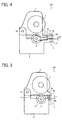
- FIG. 4 is a side view schematically illustrating the imaging unit 100 with another embodiment of the fastening mechanism F.
- the support 5 has an extension 5a held between the photoconductor housing 3 and the developer housing 6, with the foot 11 correspondingly positioned to meet the extension 5a in the closed position.
- the fastening mechanism F includes a portion 26 projecting from the photoconductor housing 3 and a portion 27 projecting from the developer housing 6, each extending beyond the extension 5a and having a screw hole to insert a screw 25 therethrough.
- the projecting portion 26 has a recessed portion 22 approximately where it extends beyond the extension 5a.
- the fastening mechanism F fastens the photoconductor housing 3 to the developer housing 6 by screwing together the portions 26 and 27, leaving a given narrow spacing S2 between the photoconductor housing 3 and the developer housing 6.
- Such screwing presses the foot 11 against the support extension 5a on each side of the imaging unit 100, thereby securely maintaining the constant gap G between the photoconductor 1 and the developer roller 4.
- the recessed portion 22 allows the portion 26 to elastically deform to accommodate the applied forces, which would otherwise deform the photoconductor housing 3.
- the clamp fastener and the screw fastener described above are superior to the elastic band fastener in terms of durability, considering that rubber loses its elasticity over time and is hard to maintain. Further, the fastening mechanism F constructed with elastic deformability prevents deformation of the housings 3 and 6 due to a mismatch between the closed position and the fastening member, which would result in concomitant defects, such as distortion of printed images, or photoconductor rotation causing abnormal sounds.
- FIG. 5 is a side view schematically illustrating the imaging unit 100 with the fastening mechanism F according to a further embodiment of this patent specification.
- the fastening mechanism F is similar to that depicted in FIG. 3 , except that the clamp 20 has no recessed portion 22 near its base, and a compressible, elastic member 40 formed of rubber or sponge rubber with a dimension greater than the spacing S1 is inserted between the photoconductor housing 3 and the developer housing 6.
- the fastening mechanism F fastens the photoconductor housing 3 to the developer housing 6 by clamping in a manner described above.
- the elastic member 40 remains compressed in the spacing S1 when the imaging unit 100 is closed and fastened, thereby preventing the clamp 20 from accidentally disengaging.
- the pressure exerted on the support 5 is adjustable by changing the dimensions and/or material of the elastic member 40. Also, the inserted elastic member 40 reduces stress on the clamp 20, which makes the fastening mechanism F less prone to breakage than the configuration of FIG. 3 where the clamp 20 integral with the photoconductor housing 3 deforms to accommodate applied forces.
- FIG. 6 is a side view schematically illustrating the imaging unit 100 with the fastening mechanism F according to a further embodiment of this patent specification.
- the fastening mechanism F is similar to that depicted in FIG. 4 , except that the projecting portion 26 has no recessed portion 22, and a compressible, elastic member 40 formed of rubber or sponge rubber with a dimension greater than the spacing S2 is inserted between the projecting portions 26 and 27.
- the fastening mechanism F fastens the photoconductor housing 3 to the developer housing 6 in a manner described above.
- the elastic member 40 remains compressed in the spacing S2 when the imaging unit 100 is closed and fastened.
- the pressure exerted on the support 5 is adjustable by changing the dimensions and/or material of the elastic member 40. Also, the inserted elastic member 40 reduces stress on the projecting portion 26, which makes the fastening mechanism F less prone to breakage than the configuration of FIG. 4 where the portion 26 integral with the photoconductor housing 3 deforms to accommodate applied forces.
- the imaging unit 100 provides the gap G between the photoconductor drum 1 and the developer roller 4 adjustable and modifiable by changing the height of the support 5. Such adjustment or modification may be done by replacing the existing support 5 with a new one, which could require costly preparation of a new mold in case the replacement is shaped by molding.
- the imaging unit 100 facilitates adjustment of the gap G through use of a plate or spacer 31 inserted between the support 5 and the photoconductor housing 3.
- FIG. 7 is a side view illustrating the imaging unit 100 of FIG. 3 provided with the spacer 31.
- the imaging unit 100 has the spacer 31 inserted between the foot 11 and the support 5, with the support 5 having a flat or moderately curved upper surface 30 to accommodate the spacer plate 31 set thereon.
- the gap G is adjustable by changing the spacer thickness C, which is less expensive than replacing the support 5.
- the spacers 31 on both sides may be independently modified to ensure that the gap G is uniform along the length of the imaging unit 100.
- FIG. 8 is a side view schematically illustrating the imaging unit 100 of FIG. 4 provided with the spacer 31.
- the imaging unit 100 has the spacer 31 inserted between the foot 11 and the support extension 5a, which has a flat upper surface to accommodate the spacer plate 31 set thereon.
- the gap G is adjustable by changing the spacer thickness C, which is less expensive than replacing the support 5 or the support extension 5a.
- the spacers 31 on both sides may be independently modified to ensure that the gap G is uniform along the length of the imaging unit 100.
- the imaging unit 100 described above is applicable to an electrophotographic image forming apparatus.
- Such application facilitates assembly and disassembly of imaging components while maintaining a consistent spacing between the photoconductor and the developer roller, thereby enhancing imaging quality and productivity of the image forming apparatus.
Landscapes
- Engineering & Computer Science (AREA)
- Computer Vision & Pattern Recognition (AREA)
- Physics & Mathematics (AREA)
- General Physics & Mathematics (AREA)
- Electrophotography Configuration And Component (AREA)
- Dry Development In Electrophotography (AREA)
Abstract
Description
- The present patent application claims priority from Japanese Patent Application No.
2007-320786 filed on December 12, 2007 - The present invention relates to an imaging unit and an image forming apparatus using the same, and more particularly, to an electrophotographic imaging unit for use in an image forming apparatus, such as a photocopier, facsimile, and printer, and an image forming apparatus using the same imaging unit.
- Electrophotographic image forming systems, such as photocopiers, facsimiles, printers, etc., employ an imaging unit in which various imaging components are assembled into a single unit. A typical architecture for electrophotographic imaging includes a photoconductor section accommodating a drum-shaped photoconductor and a developer section accommodating developer and a developer applicator or roller. When assembled, the photoconductor and the developer roller have a spacing or gap therebetween, where the developer passes from one surface to another to develop an electrostatic latent image on the photoconductor into visible form during operation.
- As variations in the development process greatly affect print quality of the image forming system, maintaining a consistent gap between the photoconductor surface and the developer roller surface is important.
- It has been a common practice to form a photoconductor drum axis or a developer roller axis movable within the accommodating section, and to adjust the movable axis relative to the other axis to obtain a desired gap between the photoconductor and the developer roller in the assembled unit. Such gap adjustment is awkward and inefficient in terms of productivity, requiring a special tool to bring the movable axis into proper position. Further, the conventional design involves complicated assembly and disassembly of imaging components, making it difficult to manufacture and maintain the imaging unit.
- To overcome such drawbacks, a hinged dual-housing imaging unit has been proposed wherein a photoconductor housing and a developer housing are connected along a common axis around which both housings are pivotable. The photoconductor housing and the developer housing rotatably hold a photoconductor drum and a developer roller, respectively, with a spacing therebetween adjustable by pivoting the housings on the common axis. Both housings have surfaces to contact or mate with each other when the imaging unit is assembled, which restrict movement or pivoting of the housings to maintain the adjusted spacing between the photoconductor drum and the developer roller. The hinged housings can be opened away from each other to facilitate assembly and disassembly of imaging components for maintenance, and the imaging unit can be restored to its proper operational position merely by contacting or mating the corresponding surfaces of the hinged housings, without any precision positioning equipment required.
- Despite its advantages over the conventional design, the above-described method based on hinged housings has a drawback in that consistency of the spacing between the photoconductor drum and the developer roller cannot be ensured because it is affected by various factors such as vertical and/or horizontal misalignment between the photoconductor and the developer roller, distortion of the accommodating housings, mismatching between the contacting or mating surfaces, etc., and is therefore hard to control. Addressing this drawback by requiring tight dimensional and positional tolerances is impractical due to high costs required to manufacture various such imaging components with high precision.
- Moreover, the above method has another drawback in that the drum-to-roller spacing, once determined, is hard to modify, since it requires modification on the contacting surface that is integral with the photoconductor or developer housing.
- Exemplary aspects of the present invention are put forward in view of the above-described circumstances, and provide a novel electrophotographic imaging unit and an image forming apparatus using the imaging unit.
- In one exemplary embodiment, the novel electrophotographic imaging unit includes a photoconductor housing, a developer housing, and a support. The photoconductor housing is configured to rotatably support a photoconductor drum. The developer housing is configured to accommodate developer and a developer roller. The support is configured to rotatably support the developer roller at opposite ends thereof. The photoconductor housing and the developer housing are hinged together at one side, and movable relative to each other at another side to open and close the imaging unit. The support is sandwiched between the photoconductor housing and the developer housing when the imaging unit is closed.
- In one exemplary embodiment, the image forming apparatus includes a electrophotographic imaging unit. The imaging unit is configured to develop an electrostatic latent image into visible form, and includes a photoconductor housing, a developer housing, and a support. The photoconductor housing is configured to rotatably support a photoconductor drum. The developer housing is configured to accommodate developer and a developer roller. The support is configured to rotatably support the developer roller at opposite ends thereof. The photoconductor housing and the developer housing are hinged together at one end, and movable relative to each other at another end to open and close the imaging unit. The support is sandwiched between the photoconductor housing and the developer housing when the imaging unit is closed.
- A more complete appreciation of the disclosure and many of the attendant advantages thereof will be readily obtained as the same becomes better understood by reference to the following detailed description when considered in connection with the accompanying drawings, wherein:
-
FIGs. 1A and 1B are perspective views schematically illustrating an electrophotographic imaging unit according to this patent specification; -
FIG. 2 is a side view schematically illustrating the imaging unit of the imaging unit ofFIGs. 1A and 1B ; -
FIG. 3 is a side view schematically illustrating the imaging unit with one embodiment of a fastening mechanism according to this patent specification; -
FIG. 4 is a side view schematically illustrating the imaging unit with another embodiment of the fastening mechanism; -
FIG. 5 is a side view schematically illustrating the imaging unit with the fastening mechanism ofFIG. 3 according to further embodiment of this patent specification; -
FIG. 6 is a side view schematically illustrating the imaging unit with the fastening mechanism ofFIG. 4 according to further embodiment of this patent specification; -
FIG. 7 is a side view illustrating the imaging unit ofFIG. 3 provided with a spacer according to this patent specification; and -
FIG. 8 is a side view schematically illustrating the imaging unit ofFIG. 4 provided with the spacer. - In describing exemplary embodiments illustrated in the drawings, specific terminology is employed for the sake of clarity. However, the disclosure of this patent specification is not intended to be limited to the specific terminology so selected, and it is to be understood that each specific element includes all technical equivalents that operate in a similar manner and achieve a similar result.
- Referring now to the drawings, wherein like reference numerals designate identical or corresponding parts throughout the several views, exemplary embodiments of the present patent application are described.
-
FIGs. 1A and 1B are perspective views schematically illustrating anelectrophotographic imaging unit 100 according to this patent specification. - As shown in
FIGs. 1A and 1B , theimaging unit 100 includes a photoconductor unit or housing 3 and a developer unit orhousing 6, fastened together by a pair ofpivot pins 10 on opposite lateral sides at one end, and movable relative to each other at another, free end. The photoconductor housing 3 has a pair of protrusions orfeet 11, one on each side, and accommodates a drum-shaped photoconductor 1 rotatable about a flanged shaft rotatably supported by a pair ofbearings 2, one on each side. Thedeveloper housing 6 holds electrophotographic developer, not shown, and has a developer applicator orroller 4 rotatable about a flanged shaft engaging a pair ofsupports 5, one on each side. - In the
imaging unit 100, thepins 10 connecting the photoconductor housing 3 and thedeveloper housing 6 define a hinge or common pivot axis parallel to the shaft of thephotoconductor drum 1, on which bothhousings 3 and 6 are pivotable to open and close theimaging unit 100 while maintaining parallel alignment between the photoconductor shaft and the developer roller shaft. - With reference to
FIG. 1B , the photoconductor housing 3 is retracted away from thedeveloper housing 6 to open theimaging unit 100. Theimaging unit 100 thus opened exposes thedeveloper roller 4 and other accommodated components for user access, allowing for ready assembly and disassembly of the internal components during maintenance. To close theimaging unit 100, the photoconductor housing 3 rotates on thepivot pins 10 toward thedeveloper housing 6, and stops where thefeet 11 meet thecorresponding supports 5 on opposite sides of theimaging unit 100. - With reference to
FIG. 1A , when theimaging unit 100 is closed, the photoconductor housing 3 and the developer housing 6 sandwich the supports 5 therebetween on both sides, with thefeet 11 resting on upper surfaces of thesupports 5 to hold a given spacing or gap G between thephono conductor drum 1 and thedeveloper roller 4. The gap G thus determined by positioning thepivotable housings 3 and 6 via thepins 10 and thesupports 5 is relatively independent of dimensional or positional variations, and is therefore more stable than that obtained by directly contacting or mating a photoconductor housing and a developer housing. - The
imaging unit 100 described above is used in an electrophotographic imaging system in its closed, operational position, where an electrostatic latent image is developed into visible form on thephotoconductor drum 1 using developer. While not depicted in the drawing, it is to be noted that theimaging unit 100 also includes a charging device, an exposure slit, and a drum cleaner, disposed around thephotoconductor 1, and a developer agitator held within thedeveloper unit 6, as well as other components involved in the electrophotographic imaging process. -
FIG. 2 is a side view schematically illustrating theimaging unit 100 in the closed position. - As shown in
FIG. 2 , the gap G between thephotoconductor drum 1 and thedeveloper roller 4 is determined as follows:
where "L" is a distance between center axes of thephotoconductor 1 and thedeveloper roller 4, "D" is a diameter of thephotoconductor drum 1, and "d" is a diameter of thedeveloper roller 4. - Assuming that the
support 5 is circular in cross-section, the distance L is given as follows:
where "A" is a distance or difference in level between the center of thephotoconductor 1 and the bottom edge of thefoot 11, and "B" is a diameter or height of thesupport 5. - According to Equations (1) and (2), the gap G is adjustable by modifying the dimensional factors A and/or B. For example, rearranging or replacing the
support 5 to change the diameter B effectively adjusts the gap G, which is relatively easy with theopenable imaging unit 100 where the hingedhousings 3 and 6 can retract away from each other to provide space for maintenance operations. - With continued reference to
FIGs. 1A, 1B , and2 , theimaging unit 100 has a fastening mechanism F at both ends in a long direction thereof, disposed on a side opposite the hinged side, used to lock the photoconductor housing 3 and thedeveloper unit 6 in the closed position. - For example, the fastening mechanism F may be
hooks 12 retaining a pair ofelastic rubber bands 13, where eachband 13 is tensioned with one end hooked to the photoconductor housing 3 and the other end hooked to thedeveloper housing 6 on each side of theclosed unit 100. - When closed and locked, the
imaging unit 100 has thefeet 11 on both sides of the photoconductor housing 3 pressed against the corresponding supports 5. Such pressure stabilizes thedeveloper roller 4 in position, which is supported in thedeveloper housing 6 without any holding mechanism except for thesupports 5. Thus, the fastening mechanism F serves to securely maintain the constant gap G between thephotoconductor drum 1 and thedeveloper roller 4 in theimaging unit 100. -
FIG. 3 is a side view schematically illustrating theimaging unit 100 with one embodiment of the fastening mechanism F. Although inFIG. 3 and in other side views theimaging unit 100 will be described with reference to one side thereof, it would be understood that theimaging unit 100 may have an identical mechanism on an opposite end thereof, and that the fastening mechanism F is provided substantially symmetrically and equidistant from a center of thephotoconductor drum 1. - As shown in
FIG. 3 , the fastening mechanism F includes aclamp 20 integrally formed with the photoconductor housing 3, and aclamp seat 21 integrally formed with thedeveloper housing 6. Theclamp 20 has atip 20a on its distal end, and a recessedportion 22 near its base or proximal end, or approximately where it begins to project from the photoconductor housing 3. - In use, the fastening mechanism F fastens the photoconductor housing 3 to the
developer housing 6 by hooking theclamp tip 20a onto theclamp seat 21, leaving a given narrow spacing S1 between the photoconductor housing 3 and thedeveloper housing 6. Such clamping presses thefoot 11 against thesupport 5 on each side of theimaging unit 100, thereby securely maintaining the constant gap G between thephotoconductor 1 and thedeveloper roller 4. - In addition, while anchoring the
tip 20a to theseat 21 applies certain forces to the fastening mechanism F, the recessedportion 22 allows theclamp 20 to elastically deform to accommodate the applied forces, which would otherwise deform the photoconductor housing 3. It is to be noted that a similar effect may be obtained by forming an elastic or deformable clamp integrally with thedeveloper housing 6 to engage a clamp seat integrally formed with the photoconductor housing 3. -
FIG. 4 is a side view schematically illustrating theimaging unit 100 with another embodiment of the fastening mechanism F. - As shown in
FIG. 4 , thesupport 5 has anextension 5a held between the photoconductor housing 3 and thedeveloper housing 6, with thefoot 11 correspondingly positioned to meet theextension 5a in the closed position. The fastening mechanism F includes aportion 26 projecting from the photoconductor housing 3 and aportion 27 projecting from thedeveloper housing 6, each extending beyond theextension 5a and having a screw hole to insert ascrew 25 therethrough. The projectingportion 26 has a recessedportion 22 approximately where it extends beyond theextension 5a. - In use, the fastening mechanism F fastens the photoconductor housing 3 to the
developer housing 6 by screwing together theportions developer housing 6. Such screwing presses thefoot 11 against thesupport extension 5a on each side of theimaging unit 100, thereby securely maintaining the constant gap G between thephotoconductor 1 and thedeveloper roller 4. - In addition, while tightening the
screw 25 in place applies certain forces to the fastening mechanism F, the recessedportion 22 allows theportion 26 to elastically deform to accommodate the applied forces, which would otherwise deform the photoconductor housing 3. - The clamp fastener and the screw fastener described above are superior to the elastic band fastener in terms of durability, considering that rubber loses its elasticity over time and is hard to maintain. Further, the fastening mechanism F constructed with elastic deformability prevents deformation of the
housings 3 and 6 due to a mismatch between the closed position and the fastening member, which would result in concomitant defects, such as distortion of printed images, or photoconductor rotation causing abnormal sounds. -
FIG. 5 is a side view schematically illustrating theimaging unit 100 with the fastening mechanism F according to a further embodiment of this patent specification. - As shown in
FIG. 5 , the fastening mechanism F is similar to that depicted inFIG. 3 , except that theclamp 20 has no recessedportion 22 near its base, and a compressible,elastic member 40 formed of rubber or sponge rubber with a dimension greater than the spacing S1 is inserted between the photoconductor housing 3 and thedeveloper housing 6. - In use, the fastening mechanism F fastens the photoconductor housing 3 to the
developer housing 6 by clamping in a manner described above. Theelastic member 40 remains compressed in the spacing S1 when theimaging unit 100 is closed and fastened, thereby preventing theclamp 20 from accidentally disengaging. - In such a configuration, the pressure exerted on the
support 5 is adjustable by changing the dimensions and/or material of theelastic member 40. Also, the insertedelastic member 40 reduces stress on theclamp 20, which makes the fastening mechanism F less prone to breakage than the configuration ofFIG. 3 where theclamp 20 integral with the photoconductor housing 3 deforms to accommodate applied forces. -
FIG. 6 is a side view schematically illustrating theimaging unit 100 with the fastening mechanism F according to a further embodiment of this patent specification. - As shown in
FIG. 6 , the fastening mechanism F is similar to that depicted inFIG. 4 , except that the projectingportion 26 has no recessedportion 22, and a compressible,elastic member 40 formed of rubber or sponge rubber with a dimension greater than the spacing S2 is inserted between the projectingportions - In use, the fastening mechanism F fastens the photoconductor housing 3 to the
developer housing 6 in a manner described above. Theelastic member 40 remains compressed in the spacing S2 when theimaging unit 100 is closed and fastened. - In such a configuration, the pressure exerted on the
support 5 is adjustable by changing the dimensions and/or material of theelastic member 40. Also, the insertedelastic member 40 reduces stress on the projectingportion 26, which makes the fastening mechanism F less prone to breakage than the configuration ofFIG. 4 where theportion 26 integral with the photoconductor housing 3 deforms to accommodate applied forces. - As mentioned, the
imaging unit 100 provides the gap G between thephotoconductor drum 1 and thedeveloper roller 4 adjustable and modifiable by changing the height of thesupport 5. Such adjustment or modification may be done by replacing the existingsupport 5 with a new one, which could require costly preparation of a new mold in case the replacement is shaped by molding. In further embodiments, theimaging unit 100 facilitates adjustment of the gap G through use of a plate orspacer 31 inserted between thesupport 5 and the photoconductor housing 3. -
FIG. 7 is a side view illustrating theimaging unit 100 ofFIG. 3 provided with thespacer 31. - As shown in
FIG. 7 , theimaging unit 100 has thespacer 31 inserted between thefoot 11 and thesupport 5, with thesupport 5 having a flat or moderately curvedupper surface 30 to accommodate thespacer plate 31 set thereon. - In such a configuration, the distance L between the center axes of the
photoconductor 1 and thedeveloper roller 4 is determined as follows:
where "A" is a distance or difference in level between the center of thephotoconductor 1 and the bottom edge of thefoot 11, "B" is a distance or difference in level between the center of thedeveloper roller 4 and the upper surface of thesupport 5, and "C" is a thickness of thespacer 31. - According to
Equations 1 and 3, the gap G is adjustable by changing the spacer thickness C, which is less expensive than replacing thesupport 5. In addition, thespacers 31 on both sides may be independently modified to ensure that the gap G is uniform along the length of theimaging unit 100. -
FIG. 8 is a side view schematically illustrating theimaging unit 100 ofFIG. 4 provided with thespacer 31. - As shown in
FIG. 8 , theimaging unit 100 has thespacer 31 inserted between thefoot 11 and thesupport extension 5a, which has a flat upper surface to accommodate thespacer plate 31 set thereon. - As in the case of
FIG. 7 , the gap G is adjustable by changing the spacer thickness C, which is less expensive than replacing thesupport 5 or thesupport extension 5a. In addition, thespacers 31 on both sides may be independently modified to ensure that the gap G is uniform along the length of theimaging unit 100. - According to this patent specification, the
imaging unit 100 described above is applicable to an electrophotographic image forming apparatus. Such application facilitates assembly and disassembly of imaging components while maintaining a consistent spacing between the photoconductor and the developer roller, thereby enhancing imaging quality and productivity of the image forming apparatus. - Numerous additional modifications and variations are possible in light of the above teachings. It is therefore to be understood that, within the scope of the appended claims, the disclosure of this patent specification may be practiced otherwise than as specifically described herein.
Claims (6)
- An electrophotographic imaging unit (100), characterized by comprising:a photoconductor housing (3) configured to rotatably support a photoconductor drum (1);a developer housing (6) configured to accommodate developer and a developer roller (4); anda support (5) configured to rotatably support the developer roller (4) at opposite ends thereof,the photoconductor housing (3) and the developer housing (6) being hinged together at one side, and movable relative to each other at another side to open and close the imaging unit (100),the support (5) being sandwiched between the photoconductor housing (3) and the developer housing (6) when the imaging unit (100) is closed.
- The imaging unit (100) according to Claim 1, characterized by further comprising a fastening mechanism (F) configured to fasten together the photoconductor housing (3) and the developer housing (6) to hold the support (5) in place when the imaging unit (100) is closed.
- The imaging unit (100) according to Claim 2, characterized in that at least one of the photoconductor housing (3) and the developer housing (6) includes an elastically deformable portion (20, 26) as part of the fastening mechanism (F) to fasten together the photoconductor housing (3) and the developer housing (6) when the imaging unit (100) is closed.
- The imaging unit (100) according to Claim 2, characterized in that the fastening mechanism (F) includes an elastically compressible member (40) inserted between the photoconductor housing (3) and the developer housing (6) when the imaging unit (100) is closed.
- The imaging unit (100) according to Claim 1, characterized by further comprising a spacer (31) inserted between the photoconductor housing (3) and the developer housing (6) to adjust spacing between the photoconductor drum (3) and the developer roller (6) when the imaging unit (100) is closed.
- An image forming apparatus, comprising:an electrophotographic imaging unit (100) configured to develop an electrostatic latent image into visible form, the imaging unit (100) including:a photoconductor housing (3) configured to rotatably support a photoconductor drum (1);a developer housing (6) configured to accommodate developer and a developer roller (4); anda support (5) configured to rotatably support the developer roller (4) at opposite ends thereof;the photoconductor housing (3) and the developer housing (6) being hinged together at one side, and movable relative to each other at another side to open and close the imaging unit (100),the support (5) being sandwiched between the photoconductor housing (3) and the developer housing (6) when the imaging unit (100) is closed.
Applications Claiming Priority (1)
| Application Number | Priority Date | Filing Date | Title |
|---|---|---|---|
| JP2007320786A JP5095376B2 (en) | 2007-12-12 | 2007-12-12 | Image forming unit and image forming apparatus |
Publications (2)
| Publication Number | Publication Date |
|---|---|
| EP2071416A1 true EP2071416A1 (en) | 2009-06-17 |
| EP2071416B1 EP2071416B1 (en) | 2019-03-06 |
Family
ID=40510394
Family Applications (1)
| Application Number | Title | Priority Date | Filing Date |
|---|---|---|---|
| EP08171330.7A Active EP2071416B1 (en) | 2007-12-12 | 2008-12-11 | Imaging unit and image forming apparatus using same |
Country Status (4)
| Country | Link |
|---|---|
| US (1) | US8351820B2 (en) |
| EP (1) | EP2071416B1 (en) |
| JP (1) | JP5095376B2 (en) |
| CN (1) | CN101458492A (en) |
Cited By (1)
| Publication number | Priority date | Publication date | Assignee | Title |
|---|---|---|---|---|
| WO2012051907A1 (en) * | 2010-10-22 | 2012-04-26 | 珠海天威飞马打印耗材有限公司 | Process cartridge |
Families Citing this family (1)
| Publication number | Priority date | Publication date | Assignee | Title |
|---|---|---|---|---|
| JP6414502B2 (en) * | 2015-03-31 | 2018-10-31 | ブラザー工業株式会社 | Process cartridge |
Citations (4)
| Publication number | Priority date | Publication date | Assignee | Title |
|---|---|---|---|---|
| US5089849A (en) | 1988-09-30 | 1992-02-18 | Kabushiki Kaisha Toshiba | Image forming apparatus, and method of positioning the units incorporated in an image forming apparatus |
| US6029031A (en) | 1995-08-25 | 2000-02-22 | Canon Kabushiki Kaisha | Process cartridge and remanufacturing method |
| US6240268B1 (en) | 1999-01-14 | 2001-05-29 | Canon Kabushiki Kaisha | Gap retaining member and developing device employing the same |
| US20020071693A1 (en) | 2000-09-11 | 2002-06-13 | Toshiba Tec Kabushiki Kaisha | Process unit, image formation device with the same and color image formation device with the same |
Family Cites Families (16)
| Publication number | Priority date | Publication date | Assignee | Title |
|---|---|---|---|---|
| JPS58113064U (en) * | 1982-01-27 | 1983-08-02 | 京セラミタ株式会社 | Electrostatic copying machine photosensitive drum support device |
| JPS58181058A (en) * | 1982-04-19 | 1983-10-22 | Mita Ind Co Ltd | Electrostatic copying machine |
| JPS63208883A (en) * | 1987-02-25 | 1988-08-30 | Canon Inc | Image carrier unit |
| JPH01217481A (en) * | 1988-02-26 | 1989-08-31 | Canon Inc | Image forming device |
| JP2628726B2 (en) * | 1988-11-15 | 1997-07-09 | 三田工業株式会社 | Image forming device |
| JP2844087B2 (en) * | 1989-08-28 | 1999-01-06 | オリンパス光学工業株式会社 | Printhead support and power supply mechanism |
| US5294960A (en) * | 1990-11-06 | 1994-03-15 | Canon Kabushiki Kaisha | Detachable two-frame process cartridge for an image forming apparatus |
| JPH05232752A (en) * | 1992-02-20 | 1993-09-10 | Ricoh Co Ltd | Image forming apparatus process cartridge |
| JPH06130799A (en) * | 1992-10-20 | 1994-05-13 | Ricoh Co Ltd | Development device |
| JPH06148969A (en) * | 1992-11-12 | 1994-05-27 | Canon Inc | Process cartridge and image forming apparatus |
| KR0122443B1 (en) | 1993-09-28 | 1997-11-17 | 김광호 | Facsimile device for general paper |
| JP3267465B2 (en) * | 1994-06-24 | 2002-03-18 | キヤノン株式会社 | Process cartridge and image forming apparatus |
| JPH09244516A (en) * | 1996-03-13 | 1997-09-19 | Mita Ind Co Ltd | Image forming device |
| JP2002108171A (en) | 2000-09-29 | 2002-04-10 | Ricoh Co Ltd | Image forming device |
| JP2006030505A (en) * | 2004-07-15 | 2006-02-02 | Fuji Xerox Co Ltd | Image forming apparatus |
| JP4927451B2 (en) * | 2006-06-16 | 2012-05-09 | 株式会社リコー | Process cartridge and image forming apparatus |
-
2007
- 2007-12-12 JP JP2007320786A patent/JP5095376B2/en active Active
-
2008
- 2008-12-11 EP EP08171330.7A patent/EP2071416B1/en active Active
- 2008-12-11 US US12/332,721 patent/US8351820B2/en not_active Expired - Fee Related
- 2008-12-12 CN CNA2008101867278A patent/CN101458492A/en active Pending
Patent Citations (4)
| Publication number | Priority date | Publication date | Assignee | Title |
|---|---|---|---|---|
| US5089849A (en) | 1988-09-30 | 1992-02-18 | Kabushiki Kaisha Toshiba | Image forming apparatus, and method of positioning the units incorporated in an image forming apparatus |
| US6029031A (en) | 1995-08-25 | 2000-02-22 | Canon Kabushiki Kaisha | Process cartridge and remanufacturing method |
| US6240268B1 (en) | 1999-01-14 | 2001-05-29 | Canon Kabushiki Kaisha | Gap retaining member and developing device employing the same |
| US20020071693A1 (en) | 2000-09-11 | 2002-06-13 | Toshiba Tec Kabushiki Kaisha | Process unit, image formation device with the same and color image formation device with the same |
Cited By (1)
| Publication number | Priority date | Publication date | Assignee | Title |
|---|---|---|---|---|
| WO2012051907A1 (en) * | 2010-10-22 | 2012-04-26 | 珠海天威飞马打印耗材有限公司 | Process cartridge |
Also Published As
| Publication number | Publication date |
|---|---|
| JP2009145467A (en) | 2009-07-02 |
| JP5095376B2 (en) | 2012-12-12 |
| US8351820B2 (en) | 2013-01-08 |
| EP2071416B1 (en) | 2019-03-06 |
| US20090154955A1 (en) | 2009-06-18 |
| CN101458492A (en) | 2009-06-17 |
Similar Documents
| Publication | Publication Date | Title |
|---|---|---|
| TWI734479B (en) | Process cartridge and image forming apparatus | |
| US6970665B2 (en) | Image forming apparatus with detachable power-requiring unit | |
| CN100449412C (en) | Image forming apparatus | |
| CN104583879A (en) | Imaging device and process cartridge | |
| US9360825B2 (en) | Cleaning device, process cartridge, and electrophotographic image forming apparatus | |
| CN111115310A (en) | Paper conveying device and image forming apparatus having the same | |
| US10037000B2 (en) | Cartridge | |
| US7957682B2 (en) | Image forming unit and image forming apparatus | |
| US8351820B2 (en) | Imaging unit and image forming apparatus that adjust and modify a gap between a photoconductor drum and a developer roller | |
| US6999709B2 (en) | Transfer unit of electrophotographic image forming appraratus | |
| RU2667311C1 (en) | Drum cylinder unit, the method of attaching the binding element and the drum unit | |
| CN101482716B (en) | Developing device and blade assembly | |
| KR200150173Y1 (en) | Doctor gap adjustment device of developer | |
| US8886109B2 (en) | Cleaning unit, process cartridge, and electrophotographic image forming apparatus | |
| JP2004144878A (en) | Image forming device | |
| JP4091740B2 (en) | Image forming apparatus | |
| JPH04147274A (en) | Process cartridge for image forming device | |
| US9304485B1 (en) | Devices and methods for remanufacturing printer cartridges | |
| US20070212138A1 (en) | Component mounting structure | |
| JP2004133077A (en) | Developing device | |
| JP2006267865A (en) | Fixing device of image forming apparatus and assembly structure of unit | |
| JPH08123292A (en) | Printer | |
| JP2020177179A (en) | Cleaning equipment, manufacturing method of cleaning equipment | |
| KR20050005175A (en) | Paper guide unit and image forming apparatus with the same | |
| JPH10173881A (en) | Image forming apparatus and writing head |
Legal Events
| Date | Code | Title | Description |
|---|---|---|---|
| PUAI | Public reference made under article 153(3) epc to a published international application that has entered the european phase |
Free format text: ORIGINAL CODE: 0009012 |
|
| AK | Designated contracting states |
Kind code of ref document: A1 Designated state(s): AT BE BG CH CY CZ DE DK EE ES FI FR GB GR HR HU IE IS IT LI LT LU LV MC MT NL NO PL PT RO SE SI SK TR |
|
| AX | Request for extension of the european patent |
Extension state: AL BA MK RS |
|
| 17P | Request for examination filed |
Effective date: 20091030 |
|
| AKX | Designation fees paid |
Designated state(s): DE FR GB |
|
| 17Q | First examination report despatched |
Effective date: 20130705 |
|
| GRAP | Despatch of communication of intention to grant a patent |
Free format text: ORIGINAL CODE: EPIDOSNIGR1 |
|
| INTG | Intention to grant announced |
Effective date: 20181012 |
|
| GRAS | Grant fee paid |
Free format text: ORIGINAL CODE: EPIDOSNIGR3 |
|
| GRAA | (expected) grant |
Free format text: ORIGINAL CODE: 0009210 |
|
| AK | Designated contracting states |
Kind code of ref document: B1 Designated state(s): DE FR GB |
|
| REG | Reference to a national code |
Ref country code: GB Ref legal event code: FG4D |
|
| REG | Reference to a national code |
Ref country code: DE Ref legal event code: R096 Ref document number: 602008059218 Country of ref document: DE |
|
| REG | Reference to a national code |
Ref country code: DE Ref legal event code: R097 Ref document number: 602008059218 Country of ref document: DE |
|
| PLBE | No opposition filed within time limit |
Free format text: ORIGINAL CODE: 0009261 |
|
| STAA | Information on the status of an ep patent application or granted ep patent |
Free format text: STATUS: NO OPPOSITION FILED WITHIN TIME LIMIT |
|
| 26N | No opposition filed |
Effective date: 20191209 |
|
| P01 | Opt-out of the competence of the unified patent court (upc) registered |
Effective date: 20230522 |
|
| PGFP | Annual fee paid to national office [announced via postgrant information from national office to epo] |
Ref country code: DE Payment date: 20241210 Year of fee payment: 17 |
|
| PGFP | Annual fee paid to national office [announced via postgrant information from national office to epo] |
Ref country code: GB Payment date: 20241224 Year of fee payment: 17 |
|
| PGFP | Annual fee paid to national office [announced via postgrant information from national office to epo] |
Ref country code: FR Payment date: 20241223 Year of fee payment: 17 |