EP2068365A2 - Semiconductor device - Google Patents
Semiconductor device Download PDFInfo
- Publication number
- EP2068365A2 EP2068365A2 EP08020442A EP08020442A EP2068365A2 EP 2068365 A2 EP2068365 A2 EP 2068365A2 EP 08020442 A EP08020442 A EP 08020442A EP 08020442 A EP08020442 A EP 08020442A EP 2068365 A2 EP2068365 A2 EP 2068365A2
- Authority
- EP
- European Patent Office
- Prior art keywords
- region
- current
- semiconductor
- semiconductor device
- hetero semiconductor
- Prior art date
- Legal status (The legal status is an assumption and is not a legal conclusion. Google has not performed a legal analysis and makes no representation as to the accuracy of the status listed.)
- Ceased
Links
Images







Classifications
-
- H—ELECTRICITY
- H10—SEMICONDUCTOR DEVICES; ELECTRIC SOLID-STATE DEVICES NOT OTHERWISE PROVIDED FOR
- H10D—INORGANIC ELECTRIC SEMICONDUCTOR DEVICES
- H10D62/00—Semiconductor bodies, or regions thereof, of devices having potential barriers
- H10D62/10—Shapes, relative sizes or dispositions of the regions of the semiconductor bodies; Shapes of the semiconductor bodies
- H10D62/13—Semiconductor regions connected to electrodes carrying current to be rectified, amplified or switched, e.g. source or drain regions
- H10D62/149—Source or drain regions of field-effect devices
- H10D62/151—Source or drain regions of field-effect devices of IGFETs
-
- H—ELECTRICITY
- H10—SEMICONDUCTOR DEVICES; ELECTRIC SOLID-STATE DEVICES NOT OTHERWISE PROVIDED FOR
- H10D—INORGANIC ELECTRIC SEMICONDUCTOR DEVICES
- H10D30/00—Field-effect transistors [FET]
- H10D30/60—Insulated-gate field-effect transistors [IGFET]
- H10D30/63—Vertical IGFETs
- H10D30/635—Vertical IGFETs having no inversion channels, e.g. vertical accumulation channel FETs [ACCUFET] or normally-on vertical IGFETs
-
- H—ELECTRICITY
- H10—SEMICONDUCTOR DEVICES; ELECTRIC SOLID-STATE DEVICES NOT OTHERWISE PROVIDED FOR
- H10D—INORGANIC ELECTRIC SEMICONDUCTOR DEVICES
- H10D62/00—Semiconductor bodies, or regions thereof, of devices having potential barriers
- H10D62/10—Shapes, relative sizes or dispositions of the regions of the semiconductor bodies; Shapes of the semiconductor bodies
- H10D62/102—Constructional design considerations for preventing surface leakage or controlling electric field concentration
- H10D62/103—Constructional design considerations for preventing surface leakage or controlling electric field concentration for increasing or controlling the breakdown voltage of reverse-biased devices
- H10D62/105—Constructional design considerations for preventing surface leakage or controlling electric field concentration for increasing or controlling the breakdown voltage of reverse-biased devices by having particular doping profiles, shapes or arrangements of PN junctions; by having supplementary regions, e.g. junction termination extension [JTE]
- H10D62/106—Constructional design considerations for preventing surface leakage or controlling electric field concentration for increasing or controlling the breakdown voltage of reverse-biased devices by having particular doping profiles, shapes or arrangements of PN junctions; by having supplementary regions, e.g. junction termination extension [JTE] having supplementary regions doped oppositely to or in rectifying contact with regions of the semiconductor bodies, e.g. guard rings with PN or Schottky junctions
- H10D62/107—Buried supplementary regions, e.g. buried guard rings
-
- H—ELECTRICITY
- H10—SEMICONDUCTOR DEVICES; ELECTRIC SOLID-STATE DEVICES NOT OTHERWISE PROVIDED FOR
- H10D—INORGANIC ELECTRIC SEMICONDUCTOR DEVICES
- H10D62/00—Semiconductor bodies, or regions thereof, of devices having potential barriers
- H10D62/10—Shapes, relative sizes or dispositions of the regions of the semiconductor bodies; Shapes of the semiconductor bodies
- H10D62/113—Isolations within a component, i.e. internal isolations
-
- H—ELECTRICITY
- H10—SEMICONDUCTOR DEVICES; ELECTRIC SOLID-STATE DEVICES NOT OTHERWISE PROVIDED FOR
- H10D—INORGANIC ELECTRIC SEMICONDUCTOR DEVICES
- H10D62/00—Semiconductor bodies, or regions thereof, of devices having potential barriers
- H10D62/10—Shapes, relative sizes or dispositions of the regions of the semiconductor bodies; Shapes of the semiconductor bodies
- H10D62/113—Isolations within a component, i.e. internal isolations
- H10D62/114—PN junction isolations
-
- H—ELECTRICITY
- H10—SEMICONDUCTOR DEVICES; ELECTRIC SOLID-STATE DEVICES NOT OTHERWISE PROVIDED FOR
- H10D—INORGANIC ELECTRIC SEMICONDUCTOR DEVICES
- H10D62/00—Semiconductor bodies, or regions thereof, of devices having potential barriers
- H10D62/10—Shapes, relative sizes or dispositions of the regions of the semiconductor bodies; Shapes of the semiconductor bodies
- H10D62/113—Isolations within a component, i.e. internal isolations
- H10D62/115—Dielectric isolations, e.g. air gaps
-
- H—ELECTRICITY
- H10—SEMICONDUCTOR DEVICES; ELECTRIC SOLID-STATE DEVICES NOT OTHERWISE PROVIDED FOR
- H10D—INORGANIC ELECTRIC SEMICONDUCTOR DEVICES
- H10D62/00—Semiconductor bodies, or regions thereof, of devices having potential barriers
- H10D62/80—Semiconductor bodies, or regions thereof, of devices having potential barriers characterised by the materials
- H10D62/82—Heterojunctions
-
- H—ELECTRICITY
- H10—SEMICONDUCTOR DEVICES; ELECTRIC SOLID-STATE DEVICES NOT OTHERWISE PROVIDED FOR
- H10D—INORGANIC ELECTRIC SEMICONDUCTOR DEVICES
- H10D62/00—Semiconductor bodies, or regions thereof, of devices having potential barriers
- H10D62/10—Shapes, relative sizes or dispositions of the regions of the semiconductor bodies; Shapes of the semiconductor bodies
- H10D62/124—Shapes, relative sizes or dispositions of the regions of semiconductor bodies or of junctions between the regions
- H10D62/126—Top-view geometrical layouts of the regions or the junctions
- H10D62/127—Top-view geometrical layouts of the regions or the junctions of cellular field-effect devices, e.g. multicellular DMOS transistors or IGBTs
-
- H—ELECTRICITY
- H10—SEMICONDUCTOR DEVICES; ELECTRIC SOLID-STATE DEVICES NOT OTHERWISE PROVIDED FOR
- H10D—INORGANIC ELECTRIC SEMICONDUCTOR DEVICES
- H10D62/00—Semiconductor bodies, or regions thereof, of devices having potential barriers
- H10D62/80—Semiconductor bodies, or regions thereof, of devices having potential barriers characterised by the materials
- H10D62/83—Semiconductor bodies, or regions thereof, of devices having potential barriers characterised by the materials being Group IV materials, e.g. B-doped Si or undoped Ge
- H10D62/832—Semiconductor bodies, or regions thereof, of devices having potential barriers characterised by the materials being Group IV materials, e.g. B-doped Si or undoped Ge being Group IV materials comprising two or more elements, e.g. SiGe
- H10D62/8325—Silicon carbide
Definitions
- the present invention relates to a semiconductor device having a heterojunction interface.
- an N - -type polycrystalline silicon region is formed to contact one main surface of a semiconductor body including an N - -type silicon carbide epitaxial region on an N + -type silicon carbide substrate.
- a heterojunction interface is formed between the epitaxial region and the polycrystalline silicon region.
- a gate electrode is formed via a gate insulating film.
- the polycrystalline silicon region is connected to a source electrode, and a bottom surface of the silicon carbide substrate is formed thereon with a drain electrode.
- the present invention has been achieved to solve the problem of the related art, and an object of the present invention is to provide a semiconductor device having a high interruption characteristic.
- a heterojunction interface that contacts a gate insulating film comprises a corner.
- a current-concentration relief region is formed. The current-concentration relief region decreases current generated at the corner than current generated at the other heterojunction interface position contacting the gate insulating film.
- a semiconductor device according to a first embodiment of the present invention is described with reference to Fig. 1 to Fig. 3 .
- Fig. 1 shows a cross-sectional structure in which semiconductor devices according to a first embodiment of the present invention are repeatedly formed, and as one example, shows a case that three semiconductor devices are aligned.
- a case that silicon carbide is a substrate material is described.
- an N + -type substrate region 1 of which the polytype of the silicon carbide is 4H type is formed thereon with an N - -type drift region 2.
- a hetero semiconductor region 3 formed of N-type polycrystalline silicon, for example, is formed to contact a main surface facing a junction surface with the substrate region 1 in the drift region 2.
- the N-type hetero semiconductor region 3 is formed to contact the N-type (first conductivity type) semiconductor body formed of the substrate region 1 and the drift region 2.
- a junction portion between the drift region 2 and the hetero semiconductor region 3 is formed by heterojunction by materials of which the band gap between the silicon carbide and the polycrystalline silicon differs, and at a heterojunction interface, an energy barrier exists.
- a source electrode 6 is formed through a contact hole b to provide an ohmic connection.
- a drain electrode 7 is formed to provide an ohmic connection.
- An interlayer insulating film 8 is formed to insulate between the gate electrode 5 and the source electrode 6.
- a plurality of base cell structures of the semiconductor device configured by each of the regions 1 to 8 are arranged as in a surface shape shown in Fig. 2 , for example, to form a semiconductor chip 100.
- Fig. 2 to easily understand the surface arrangement of the heterojunction driving end a1 shown in Fig. 1 , illustrations of the gate insulating film 4, the gate electrode 5, the source electrode 6, and the interlayer insulating film 8 are omitted.
- a cross-sectional structure taken along A-A in Fig. 2 is the cross-sectional structure shown in Fig. 1 . As shown in Fig.
- a groove (hole) for forming the gate insulating film 4 placed in the hetero semiconductor region 3 is a linear shape extending in right and left directions and up and down directions in the plan of the paper, and the surface shape of the hetero semiconductor region 3 is in a square cell shape.
- the heterojunction driving end a1 has a convex corner.
- the hetero semiconductor corner regions 10 formed of P - -type polycrystalline silicon of which the conductivity type is opposite to and the impurity density is smaller than those of the hetero semiconductor region 3, for example.
- the hetero semiconductor corner regions 10 contacting the convex corners are formed in the hetero semiconductor region 3, and configures a heterojunction driving end a2 so that the hetero semiconductor corner regions 10 contacts the gate insulating film 4 and the drift region 2, respectively, as shown in a cross-sectional structure of the four corners of the hetero semiconductor region 3 in Fig. 3 , which shows a cross-sectional shape taken along B-B in Fig. 2 .
- the semiconductor device is so used that the source electrode 6 is grounded and the drain electrode 7 is applied a positive potential, for example.
- the gate electrode 5 is grounded or a negative potential, for example, an interrupted state is held. That is, this is due to the fact that at the heterojunction interface between the hetero semiconductor region 3 and the hetero semiconductor connecting region 10, and the drift region 2, the energy barrier for a conduction electron is formed.
- the hetero semiconductor corner regions 10 formed of P-type polycrystalline silicon are arranged. Thus, even when the convex corners are provided, a large leakage current is not generated. As a result, the interruption characteristic provided in the base cell structure shown in Fig. 1 can also be obtained in the semiconductor chip 100.
- the hetero semiconductor corner regions 10 formed of P - -type polycrystalline silicon are arranged to form the heterojunction driving end a2 at the four corners of the hetero semiconductor region 3, two leakage-current decreasing effects can be obtained.
- the hetero semiconductor corner region 10 is opposite in conductivity type to the hetero semiconductor region 3, and thus, the energy barrier for the conduction electron, formed at the heterojunction interface between the hetero semiconductor corner region 10 and the drift region 2, is formed to be higher than the energy barrier formed at the heterojunction interface between the hetero semiconductor region 3 and the drift region 2.
- the energy barrier formed at the heterojunction interface becomes higher in order of conductivity type of: P + -type, P - -type, intrinsic, N - -type, and N + -type.
- Second reason for this is that since the impurity density of the hetero semiconductor corner region 10 is smaller than that of the hetero semiconductor region 3, a resistance of the hetero semiconductor corner region 10 is larger than that of the hetero semiconductor region 3, and as a result, a resistance at the convex corner is large. Due to these reasons, according to the first embodiment, the interrupting performance can be further improved than that of the conventional technique.
- the heterojunction driving end a1 of the hetero semiconductor region 3 and a surface layer portion of the drift region 2 where the gate electric field applies via the gate insulating film 4 are formed thereon with an accumulation layer of electrons.
- a potential becomes to be the one that a free electron can be present, which makes the energy barrier extending to a side of the drift region 2 steep. Thereby, a thickness of the energy barrier is decreased. As a result, an electron current is conducted.
- the hetero semiconductor corner regions 10 are arranged in the convex corners, the energy barrier for the conduction electron, formed at the heterojunction interface, is formed to be higher than the other portions, and a resistance in a conductive path is formed to be large.
- the current does not concentrate on the convex corners, and most of the current that passes at the time of conduction is passed nearly uniformly in the base cell formed of the regions 1 to 8 arranged in plural and in parallel.
- a semiconductor chip 100 in which the hot spot where a specific location generates heat is not easily generated can be obtained.
- a reverse conduction (back-flow operation) in which the source electrode 6 is grounded and a negative potential is applied to the drain electrode 7 can also be possible.
- the source electrode 6 and the gate electrode 5 are grounded and a predetermined positive potential is applied to the drain electrode 7, the energy barrier for the conduction electron vanishes and the conduction electron passes from the side of the drift region 2 to the side of the hetero semiconductor region 3, resulting in a reverse conducting state.
- the conduction is achieved only by the conduction electron without hole injection, and thus, a loss caused by a reverse recovery current at the time of transferring from the reverse conducting state to the interrupted state is also small.
- the gate electrode 5 can be used as a control electrode without being grounded.
- the current does not concentrate on the convex corners. Most of the current that passes at the time of reverse conduction is passed nearly uniformly in the base cell structure formed of the regions 1 to 8 arranged in plural and in parallel, and thus, the current is not concentrated on a specific portion.
- the hetero semiconductor corner region 10 which is the current-concentration relief region that keeps a reverse bias current from concentrating on the convex corner, is arranged in the hetero semiconductor region 3, and thereby, a current concentration on the convex corner can be prevented.
- an interrupting performance can be improved at the time of interruption, and at the same time, the generation of the hot spot where in a specific portion is prevented at the time of conduction to suppress deterioration in a specific portion, thereby ensuring a long-term reliability.
- the semiconductor chip 100 when used in an L load circuit or the like, for example, at the time of conduction or during a transient response time to the interrupted state, in an index such as a short resistant load amount and an avalanche resistant amount, which are indexes of a breakdown tolerance when overcurrent or overvoltage occurs, the current concentration on a specific portion can be prevented, and thus, these breakdown tolerances can also be improved.
- an index such as a short resistant load amount and an avalanche resistant amount, which are indexes of a breakdown tolerance when overcurrent or overvoltage occurs
- the first embodiment is so described that the hetero semiconductor corner region 10 is P - -type.
- the effect of the present invention can be obtained.
- the hetero semiconductor region 3 described in the first embodiment is N-type, if a condition other than N + -type, in which the impurity density is higher than that of the hetero semiconductor region 3, is satisfied, the effect can be exhibited at least.
- the surface shape of the hetero semiconductor corner region 10 is in a triangle shape.
- the surface shape of the hetero semiconductor corner region can take any shape such as a square shape and a sector shape.
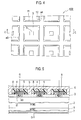
- a semiconductor device according to a second embodiment of the present invention is described with reference to Figs. 4,5 .
- the hetero semiconductor corner region 10 contacting the convex corner is formed in the hetero semiconductor region 3.
- a hetero semiconductor driving region 11 contacting a heterojunction driving end a3 other than the convex corner can be formed in the hetero semiconductor region 3 in the semiconductor chip 102. That is, in a portion contacting the heterojunction driving end a3 other than the convex corner in the hetero semiconductor region 3, a hetero semiconductor driving region 11 of which at least one of the conductivity type and the impurity density is different from those of the hetero semiconductor region 3 is formed.
- a hetero semiconductor corner region 12 of which the conductivity type and the impurity density are the same as those of the hetero semiconductor region 3 is formed.
- the hetero semiconductor driving region 11 is N + -type of which the impurity density is higher than that of the hetero semiconductor region 3
- the hetero semiconductor corner region 12 is higher in energy barrier than the hetero semiconductor driving region 11 and larger in resistance due to its small impurity density.
- the current concentration at the convex corner can be decreased.
- the hetero semiconductor driving region 11 which is the current-concentration relief region that keeps the reverse bias current from concentrating on the convex corner, in a portion other than at the convex corner. Even in this case, the effect of the present invention can be obtained.
- the hetero semiconductor driving region 11 contacting the heterojunction driving end a3 other than the convex corner is formed in the hetero semiconductor region 3.
- the energy barrier for the conduction electron, formed at the heterojunction interface between the hetero semiconductor driving region 11 and the drift region 2 is lowered than the energy barrier formed at the heterojunction interface between the hetero semiconductor corner region 12 (hetero semiconductor region 3) and the drift region 2.
- the hetero semiconductor driving region 11 can be a conductivity type opposite to that of the hetero semiconductor corner region 12 (hetero semiconductor region 3).
- the resistance of the hetero semiconductor driving region 11 is decreased than that of the hetero semiconductor corner region 12 (hetero semiconductor region 3).
- the impurity density of the hetero semiconductor driving region 11 can be decreased than that of the hetero semiconductor corner region 12 (hetero semiconductor region 3).
- a semiconductor device according to a third embodiment of the present invention is described with reference to Figs. 6,7 .
- the surface shape of the hetero semiconductor region 3 is in a square cell shape, and the convex corner of the heterojunction driving end a1 is provided.
- a well region 13 made of silicon carbide of which the conductivity type, i.e., P-type (second conductivity type), is opposite to and the impurity density is larger than those of the drift region 2 is formed in the drift region 2 to contact the convex corner of the heterojunction driving end a1, for example. That is, as shown in Fig. 7 showing a cross-sectional structure taken along D-D in Fig.
- the well region 13 is formed in the drift region 2 to contact the hetero semiconductor region 3 and the gate insulating film 4, thereby configuring the heterojunction driving end a1. That is, in a portion at which a groove for the gate insulating film 4 in right and left directions in the plane of the paper of Fig. 6 in the drift region 2 and a groove for the gate insulating film 4 in up and down directions in the plane of the paper thereof intersect, the well region 13 is formed, and the corner of the hetero semiconductor region 3 and the corner of the well region 13 are superposed on the plane of the paper in Fig. 6 .
- the semiconductor device is so used that the source electrode 6 is grounded and the drain electrode 7 is applied a positive potential, for example.
- the heterojunction driving end a1 of the hetero semiconductor region 3 and the surface layer portion of the drift region 2 where the gate electric field applies via the gate insulating film 4 is formed thereon with an accumulation layer of electrons.
- a potential becomes to be the one that a free electron can be present, which makes the energy barrier extending to a side of the drift region 2 steep.
- a thickness of the energy barrier is decreased.
- an electron current is conducted.
- a PN junction is formed in a path passing through the convex corner.
- the semiconductor chip 103 when the semiconductor chip 103 is used in an L load circuit or the like, for example, at the time of conduction or during a transient response time to the interrupted state, in an index such as a short resistant load amount and an avalanche resistant amount, which are indexes of a breakdown tolerance when overcurrent or overvoltage occurs, the current concentration on a specific portion can be prevented. Thus, these breakdown tolerances can also be improved.
- the shape of the well region 13 shown in Fig. 6 is square. However, the well region in an X-letter shape can be formed. A hole can be provided in a predetermined portion of the well region. Other shapes can be selected. In any shape, as long as the well region 13 contacts at least the convex corner (the four corners of the hetero semiconductor region 3) of the heterojunction driving end a1, the effect of the present invention can be obtained.
- a semiconductor device according to a fourth embodiment of the present invention is described with reference to Figs. 8,9 .
- a high-resistance region 14 which is formed as an inactive region by implantation of a predetermined ion in the drift region 2 and of which the conductivity is smaller than that of the drift region 2, is formed to contact the convex corner of the heterojunction driving end a1, a similar effect can be obtained.
- a high-resistance region 14 having a resistance extremely higher than those of other portions is formed in the drift region 2.
- the high-resistance region 14 which is the current-concentration relief region that keeps the reverse bias current from concentrating on the convex corner is arranged in the drift region 2 to contact the convex corner (four corners of the hetero semiconductor region 3) of the heterojunction driving end a1
- the current concentration on the convex corner can be prevented.
- an interrupting performance can be improved at the time of interruption, and at the same time, the generation of the hot spot in a specific portion is prevented at the time of conduction to suppress deterioration in the specific portion, thereby ensuring a long-term reliability.
- a semiconductor device according to a fifth embodiment of the present invention is described with reference to Figs. 10,11 .
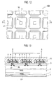
- an insulating region 15a is formed in the drift region 2 to contact the convex corner of the heterojunction driving end a1. That is, in a semiconductor chip 105, between the four corners of the hetero semiconductor region 3 and the drift region 2, an insulating region 15a formed of silicon oxide film, for example, is formed. As a result of the insulating region 15a which is the current-concentration relief region that keeps a reverse bias current from concentrating on the convex corner, no current is passed between the four corners of the hetero semiconductor region 3 and the drift region 2. Thereby, the current concentration on the convex corner can be avoided, and thus, the effect of the present invention can be obtained.
- a semiconductor device according to a sixth embodiment of the present invention is described with reference to Figs. 12,13 .
- a case that the current-concentration relief region is formed in the drift region 2 in a manner to contact the convex corner of the heterojunction driving end a1 (four corners of the hetero semiconductor region 3) has been exemplified for description.
- a sixth embodiment of the present invention for example, as shown in Fig. 12 and Fig. 13 showing a cross-sectional structure taken along G-G in Fig. 12 , even when a conductive region 16, of which the conductivity type is the same as and the impurity density is larger than that of the drift region 2, is formed to contact the heterojunction driving end a1 other than the convex corner, the effect of the present invention can be obtained.
- the conductive region 16 which is the current-concentration relief region that keeps a reverse bias current from concentrating on the convex corner is formed in a manner to contact the heterojunction driving end a1 other than the convex corner.
- a semiconductor device according to a seventh embodiment of the present invention is described with reference to Fig. 14 .
- the insulating region 15a is formed within the drift region 2.
- the insulating region 15b can be formed on the drift region 2 in a manner to contact the convex corner of the heterojunction driving end a1. That is, between the four corners of the hetero semiconductor region 3, and the drift region 2, an insulating region 15b formed of a silicon oxide film, for example, is formed.
- a surface structure of the seventh embodiment is similar to that in Fig. 10 .
- the insulating region 15b which is the current-concentration relief region that keeps a reverse bias current from concentrating on the convex corner, no current is passed between the four corners of the hetero semiconductor region 3, and the drift region 2. Thereby, the current concentration on the convex corner can be avoided, and thus, the effect of the present invention can be obtained.
- a minimum configuration is used to describe the base cell structure.
- the current concentration caused in at least one portion of the heterojunction driving end a1 can be relieved at the time of interruption and conduction, even when any structure is added as the semiconductor device or even when the semiconductor device is modified in any shape, the similar effect can be obtained.
- the cross-sectional structures of the hetero semiconductor region 3 shown in the first to seventh embodiments a case that side surfaces, i.e., up-and-down-direction surfaces in the plane of paper of Fig. 14 , of the hetero semiconductor region 3 forms a right angle relative to a surface of the drift region 2 is described.
- the side surfaces of the hetero semiconductor region 3 can form an acute angle or an obtuse angle relative to the surface of the drift region 2.
- a case of a so-called planar type in which the gate electrode 5 is formed without drilling the drift region 2 is described.
- a so-called trench type in which the drift region 2 is drilled can be selected.
- Fig. 1 which exemplifies as the base cell
- a case that the hetero semiconductor region 3 is configured by a single impurity region is shown.
- the hetero semiconductor region 3 can be configured by a plurality of impurity regions. That is, as shown in Fig.
- a P + -type second hetero semiconductor region 18, of which the conductivity type is opposite to and the impurity density is higher than those of the hetero semiconductor region 3, is formed in the hetero semiconductor region 3 apart from the gate insulating film 4, the interrupting performance of the base cell is improved, and at the same time, as the semiconductor chip, a leakage current can be further decreased.
- the current-concentration relief region can be formed in the drift region 2 of the base cell structure. That is, as shown in Fig. 18 , a well region 19 can be formed in the drift region 2 in a manner to contact the hetero semiconductor region 3, for example. At this time, for example, similarly to the third embodiment, the well region 13 is formed in the drift region 2, as shown in Fig. 19 . In this case, in respective predetermined portions of the hetero semiconductor 3, well regions 13 and 19 can be formed by the same process.
- a cross-sectional structure taken along H-H in Fig. 19 is a cross-sectional shape shown in Fig. 18 .
- a cross-sectional structure taken along D-D in Fig. 19 is similar to the cross-sectional structure shown in Fig.
- the well region 19 is formed to contact the hetero semiconductor region 3.
- the well region 20 can be formed to contact the gate insulating film 4. In any structure or in any combined shape, in addition to exhibiting the effect of the present invention, the interrupting performance can be further improved.
- the well region 13 is formed to contact the concave corner of the outermost heterojunction driving end a1 in a stripe shape, shown in a region R2 in Fig. 23 , for example.
- the surface shape of the hetero semiconductor region 3 it is possible not to allow the current to pass to a portion having a curvature or a corner different from that in other portions.
- the cell shape as one example of the cell shape, a case of the square cell shape is shown for description.
- a convex corner of the heterojunction driving end a1 such as a hexagonal cell shape and a circle cell shape, or a surface arrangement having a concave corner is adopted, any shape can provide the effect of the present invention.
- the convex corner a case of the right-angle shape is exemplified.
- the effect of the present invention can be obtained.
- measures for relieving the current concentration in a predetermined portion of the hetero semiconductor region 3 are individually shown, these measures can be used in combination.
- the present invention is not limited to the descriptions and the drawings, which form a part of the disclosure of the present invention according to these embodiments.
- the substrate material can be other semiconductor materials such as gallium nitride and diamond.
- the first to seventh embodiments are described by using 4H type as the polytype of silicon carbide. However, other polytypes such as 6H and 3C can be selected.
- the first to seventh embodiments are described by using a so-called vertically structured transistor in which the drain electrode 7 and the source electrode 6 are arranged to be opposite to each other in a manner to sandwich the drift region 2 therebetween and the current is passed vertically.
- a so-called horizontally structured transistor in which for example, the drain electrode 7 and the source electrode 6 are arranged on the same main surface and the current is passed in a horizontal direction can also be selected.
- the material used for the hetero semiconductor region 3 an example using the polycrystalline silicon is described.
- any material including other silicon materials such as single crystal silicon and amorphous silicon, other semiconductor materials such as germanium and silicon germane, and other polytypes of silicon carbide such as 6H and 3C can be selected.
- the present invention is described by using, as one example, the N-type silicon carbide as the drift region 2 and the N-type polycrystalline silicon as the hetero semiconductor region 3.
- any combination of N-type silicon carbide and P-type polycrystalline silicon, that of P-type silicon carbide and P-type polycrystalline silicon, and that of P-type silicon carbide and N-type polycrystalline silicon can be selected.
Landscapes
- Junction Field-Effect Transistors (AREA)
- Semiconductor Integrated Circuits (AREA)
- Electrodes Of Semiconductors (AREA)
Abstract
Description
- The present invention relates to a semiconductor device having a heterojunction interface.
- Conventionally, a semiconductor device disclosed in Japanese Patent Application Laid-open No.
2003-318398 - When a circuit is configured by arranging the semiconductor device in plural and in parallel, polycrystalline silicon regions of adjacent semiconductor devices are arranged separate with each other. Therefore, a level difference of the heterojunction interface is generated at the end of the heterojunction interface. As a result, when a reverse bias voltage is applied such as at the time of interruption, a leakage current concentration occurs in a region where the level difference is generated as compared to the other heterojunction interface region. Thus, there is a problem that an interruption characteristic is decreased as a semiconductor device.
- The present invention has been achieved to solve the problem of the related art, and an object of the present invention is to provide a semiconductor device having a high interruption characteristic.
- According to the present invention, a heterojunction interface that contacts a gate insulating film comprises a corner. A current-concentration relief region is formed. The current-concentration relief region decreases current generated at the corner than current generated at the other heterojunction interface position contacting the gate insulating film.
- Exemplary embodiments of the invention will become more fully apparent from the following description and appended claims, taken in conjunction with the accompanying drawings. Understanding that these drawings depict only exemplary embodiments and are, therefore, not to be considered limiting of the invention's scope, the exemplary embodiments of the invention will be described with additional specificity and detail through use of the accompanying drawings in which:
-
Fig. 1 is a cross-sectional view of a semiconductor device according to a first embodiment of the present invention; -
Fig. 2 is a surface view of a semiconductor device according to a first embodiment of the present invention; -
Fig. 3 is a cross-sectional view of a semiconductor device according to a first embodiment of the present invention; -
Fig. 4 is a surface view of a semiconductor device according to a second embodiment of the present invention; -
Fig. 5 is a cross-sectional view of a semiconductor device according to a second embodiment of the present invention; -
Fig. 6 is a surface view of a semiconductor device according to a third embodiment of the present invention; -
Fig. 7 is a cross-sectional view of a semiconductor device according to a third embodiment of the present invention; -
Fig. 8 is a surface view of a semiconductor device according to a fourth embodiment of the present invention; -
Fig. 9 is a cross-sectional view of a semiconductor device according to a fourth embodiment of the present invention; -
Fig. 10 is a surface view of a semiconductor device according to a fifth embodiment of the present invention; -
Fig. 11 is a cross-sectional view of a semiconductor device according to a fifth embodiment of the present invention; -
Fig. 12 is a surface view of a semiconductor device according to a sixth embodiment of the present invention; -
Fig. 13 is a cross-sectional view of a semiconductor device according to a sixth embodiment of the present invention; -
Fig. 14 is a cross-sectional view of a semiconductor device according to a seventh embodiment of the present invention; -
Fig. 15 is a cross-sectional view of a semiconductor device according to other embodiment of the present invention; -
Fig. 16 is a cross-sectional view of a semiconductor device according to other embodiment of the present invention; -
Fig. 17 is a cross-sectional view of a semiconductor device according to other embodiment of the present invention; -
Fig. 18 is a cross-sectional view of a semiconductor device according to other embodiment of the present invention; -
Fig. 19 is a surface view of a semiconductor device according to other embodiment of the present invention; -
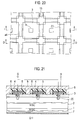
Fig. 20 is a surface view of a semiconductor device according to other embodiment of the present invention; -
Fig. 21 is a cross-sectional view of a semiconductor device according to other embodiment of the present invention; -
Fig. 22 is a surface view of a semiconductor device according to other embodiment of the present invention; and -
Fig. 23 is a surface view of a semiconductor device according to other embodiment of the present invention. - Preferred embodiments of the present invention will be explained below with reference to the accompanying drawings.
- A semiconductor device according to a first embodiment of the present invention is described with reference to
Fig. 1 to Fig. 3 . -
Fig. 1 shows a cross-sectional structure in which semiconductor devices according to a first embodiment of the present invention are repeatedly formed, and as one example, shows a case that three semiconductor devices are aligned. In the first embodiment, as one example, a case that silicon carbide is a substrate material is described. According to the first embodiment, as shown inFig. 1 , an N+-type substrate region 1 of which the polytype of the silicon carbide is 4H type is formed thereon with an N--type drift region 2. Ahetero semiconductor region 3 formed of N-type polycrystalline silicon, for example, is formed to contact a main surface facing a junction surface with thesubstrate region 1 in thedrift region 2. That is, the N-typehetero semiconductor region 3 is formed to contact the N-type (first conductivity type) semiconductor body formed of thesubstrate region 1 and thedrift region 2. A junction portion between thedrift region 2 and thehetero semiconductor region 3 is formed by heterojunction by materials of which the band gap between the silicon carbide and the polycrystalline silicon differs, and at a heterojunction interface, an energy barrier exists. - A
gate insulating film 4 formed of a silicon oxide film, for example, is formed to contact the heterojunction interface between thehetero semiconductor region 3 and thedrift region 2. That is, a hole that reaches thedrift region 2 is placed in thehetero semiconductor region 3, and thegate insulating film 4 is formed on a top surface of thehetero semiconductor region 3, side surfaces of the hole, and a surface of the hole of thedrift region 2. Out of the heterojunction surface between thehetero semiconductor region 3 and thedrift region 2, a portion contacting thegate insulating film 4 is called a "heterojunction driving end a1". On thegate insulating film 4, agate electrode 5 is formed. On an opposite surface facing the heterojunction surface between thehetero semiconductor region 3 and thedrift region 2, asource electrode 6 is formed through a contact hole b to provide an ohmic connection. In thesubstrate region 1, adrain electrode 7 is formed to provide an ohmic connection. An interlayer insulatingfilm 8 is formed to insulate between thegate electrode 5 and thesource electrode 6. - A plurality of base cell structures of the semiconductor device configured by each of the
regions 1 to 8 are arranged as in a surface shape shown inFig. 2 , for example, to form asemiconductor chip 100. InFig. 2 , to easily understand the surface arrangement of the heterojunction driving end a1 shown inFig. 1 , illustrations of thegate insulating film 4, thegate electrode 5, thesource electrode 6, and theinterlayer insulating film 8 are omitted. A cross-sectional structure taken along A-A inFig. 2 is the cross-sectional structure shown inFig. 1 . As shown inFig. 2 , in the first embodiment, a groove (hole) for forming thegate insulating film 4 placed in thehetero semiconductor region 3 is a linear shape extending in right and left directions and up and down directions in the plan of the paper, and the surface shape of thehetero semiconductor region 3 is in a square cell shape. Thus, the heterojunction driving end a1 has a convex corner. However, at the four corners of thehetero semiconductor region 3, i.e., portions contacting the convex corner of the heterojunction driving end a1, there are formed heterosemiconductor corner regions 10 formed of P--type polycrystalline silicon of which the conductivity type is opposite to and the impurity density is smaller than those of thehetero semiconductor region 3, for example. That is, the heterosemiconductor corner regions 10 contacting the convex corners are formed in thehetero semiconductor region 3, and configures a heterojunction driving end a2 so that the heterosemiconductor corner regions 10 contacts thegate insulating film 4 and thedrift region 2, respectively, as shown in a cross-sectional structure of the four corners of thehetero semiconductor region 3 inFig. 3 , which shows a cross-sectional shape taken along B-B inFig. 2 . - The operation is described next. In the first embodiment, the semiconductor device is so used that the
source electrode 6 is grounded and thedrain electrode 7 is applied a positive potential, for example. - First, when the
gate electrode 5 is grounded or a negative potential, for example, an interrupted state is held. That is, this is due to the fact that at the heterojunction interface between thehetero semiconductor region 3 and the heterosemiconductor connecting region 10, and thedrift region 2, the energy barrier for a conduction electron is formed. At this time, in the first embodiment, at the four corners of thehetero semiconductor region 3 in a square cell shape, the heterosemiconductor corner regions 10 formed of P-type polycrystalline silicon are arranged. Thus, even when the convex corners are provided, a large leakage current is not generated. As a result, the interruption characteristic provided in the base cell structure shown inFig. 1 can also be obtained in thesemiconductor chip 100. The reason for this is that when the heterosemiconductor corner regions 10 formed of P--type polycrystalline silicon are arranged to form the heterojunction driving end a2 at the four corners of thehetero semiconductor region 3, two leakage-current decreasing effects can be obtained. First reason for this is that the heterosemiconductor corner region 10 is opposite in conductivity type to thehetero semiconductor region 3, and thus, the energy barrier for the conduction electron, formed at the heterojunction interface between the heterosemiconductor corner region 10 and thedrift region 2, is formed to be higher than the energy barrier formed at the heterojunction interface between thehetero semiconductor region 3 and thedrift region 2. For example, when the conductivity type of thedrift region 2 is N-type, the energy barrier formed at the heterojunction interface becomes higher in order of conductivity type of: P+-type, P--type, intrinsic, N--type, and N+-type. Second reason for this is that since the impurity density of the heterosemiconductor corner region 10 is smaller than that of thehetero semiconductor region 3, a resistance of the heterosemiconductor corner region 10 is larger than that of thehetero semiconductor region 3, and as a result, a resistance at the convex corner is large. Due to these reasons, according to the first embodiment, the interrupting performance can be further improved than that of the conventional technique. - Next, when a positive potential is applied to the
gate electrode 5 to shift from the interrupted state to the conducting state, the heterojunction driving end a1 of thehetero semiconductor region 3 and a surface layer portion of thedrift region 2 where the gate electric field applies via thegate insulating film 4 are formed thereon with an accumulation layer of electrons. As a result, in thehetero semiconductor region 3 and the surface layer portion of thedrift region 2, a potential becomes to be the one that a free electron can be present, which makes the energy barrier extending to a side of thedrift region 2 steep. Thereby, a thickness of the energy barrier is decreased. As a result, an electron current is conducted. At this time, in the first embodiment, the heterosemiconductor corner regions 10 are arranged in the convex corners, the energy barrier for the conduction electron, formed at the heterojunction interface, is formed to be higher than the other portions, and a resistance in a conductive path is formed to be large. Thus, the current does not concentrate on the convex corners, and most of the current that passes at the time of conduction is passed nearly uniformly in the base cell formed of theregions 1 to 8 arranged in plural and in parallel. As a result, asemiconductor chip 100 in which the hot spot where a specific location generates heat is not easily generated can be obtained. That is, in contrast to a case that the heterosemiconductor corner region 10 is not arranged, even when the conduction and the interruption are repeated, a specific location is not easily deteriorated. Thus, it is possible to improve a breakdown tolerance such as a short resistant load amount, and a performance about a long-term reliability as well. - Next, in the first embodiment, to shift from the conducting state to the interrupted state, when the
gate electrode 5 is again grounded, an accumulated state of the conduction electron formed at the heterojunction interface between thehetero semiconductor region 3 and thedrift region 2 is released, and thus, tunneling in the energy barrier is stopped. Thereafter, when passing of the conduction electron from thehetero semiconductor region 3 to thedrift region 2 is stopped, and the conduction electron remaining in thedrift region 2 is depleted as a result of being passed to thesubstrate region 1, a depletion layer expands from the heterojunction portion to a side of thedrift region 2, resulting in an interrupted state. - In the first embodiment, for example, a reverse conduction (back-flow operation) in which the
source electrode 6 is grounded and a negative potential is applied to thedrain electrode 7 can also be possible. For example, when thesource electrode 6 and thegate electrode 5 are grounded and a predetermined positive potential is applied to thedrain electrode 7, the energy barrier for the conduction electron vanishes and the conduction electron passes from the side of thedrift region 2 to the side of thehetero semiconductor region 3, resulting in a reverse conducting state. At this time, the conduction is achieved only by the conduction electron without hole injection, and thus, a loss caused by a reverse recovery current at the time of transferring from the reverse conducting state to the interrupted state is also small. Alternatively, thegate electrode 5 can be used as a control electrode without being grounded. At the time of a reverse conduction (flow-back operation), in the first embodiment, the current does not concentrate on the convex corners. Most of the current that passes at the time of reverse conduction is passed nearly uniformly in the base cell structure formed of theregions 1 to 8 arranged in plural and in parallel, and thus, the current is not concentrated on a specific portion. - Thus, the hetero
semiconductor corner region 10, which is the current-concentration relief region that keeps a reverse bias current from concentrating on the convex corner, is arranged in thehetero semiconductor region 3, and thereby, a current concentration on the convex corner can be prevented. As a result, an interrupting performance can be improved at the time of interruption, and at the same time, the generation of the hot spot where in a specific portion is prevented at the time of conduction to suppress deterioration in a specific portion, thereby ensuring a long-term reliability. Further, when thesemiconductor chip 100 is used in an L load circuit or the like, for example, at the time of conduction or during a transient response time to the interrupted state, in an index such as a short resistant load amount and an avalanche resistant amount, which are indexes of a breakdown tolerance when overcurrent or overvoltage occurs, the current concentration on a specific portion can be prevented, and thus, these breakdown tolerances can also be improved. - The first embodiment is so described that the hetero
semiconductor corner region 10 is P--type. However, when one of the conditions, i.e., that the energy barrier is high and that the resistance is large, is satisfied so that the current generated in the heterojunction driving end a2 formed by the heterosemiconductor connecting region 10 is smaller than that generated in the heterojunction driving end a1 formed by thehetero semiconductor region 3 of the base cell, the effect of the present invention can be obtained. For example, when thehetero semiconductor region 3 described in the first embodiment is N-type, if a condition other than N+-type, in which the impurity density is higher than that of thehetero semiconductor region 3, is satisfied, the effect can be exhibited at least.Fig. 2 exemplifies a case that the surface shape of the heterosemiconductor corner region 10 is in a triangle shape. However, as long as the convex corner can be contacted, the surface shape of the hetero semiconductor corner region can take any shape such as a square shape and a sector shape. - A semiconductor device according to a second embodiment of the present invention is described with reference to
Figs. 4,5 . - In the first embodiment, the hetero
semiconductor corner region 10 contacting the convex corner is formed in thehetero semiconductor region 3. However, for example, as a second embodiment of the present invention, as shown inFig. 4 and Fig. 5 showing a cross-sectional structure taken along C-C inFig. 4 , a heterosemiconductor driving region 11 contacting a heterojunction driving end a3 other than the convex corner can be formed in thehetero semiconductor region 3 in thesemiconductor chip 102. That is, in a portion contacting the heterojunction driving end a3 other than the convex corner in thehetero semiconductor region 3, a heterosemiconductor driving region 11 of which at least one of the conductivity type and the impurity density is different from those of thehetero semiconductor region 3 is formed. In a portion contacting the heterojunction driving end a4 at the convex corner, a heterosemiconductor corner region 12 of which the conductivity type and the impurity density are the same as those of thehetero semiconductor region 3 is formed. For example, when the heterosemiconductor driving region 11 is N+-type of which the impurity density is higher than that of thehetero semiconductor region 3, even if the conductivity type of the heterosemiconductor corner region 12 is N-type, the same as that of thehetero semiconductor region 3, the heterosemiconductor corner region 12 is higher in energy barrier than the heterosemiconductor driving region 11 and larger in resistance due to its small impurity density. The current concentration at the convex corner can be decreased. That is, it can be possible to use a method for creating the heterosemiconductor driving region 11, which is the current-concentration relief region that keeps the reverse bias current from concentrating on the convex corner, in a portion other than at the convex corner. Even in this case, the effect of the present invention can be obtained. - Thus, according to the second embodiment, as the current-concentration relief region, the hetero
semiconductor driving region 11 contacting the heterojunction driving end a3 other than the convex corner is formed in thehetero semiconductor region 3. The energy barrier for the conduction electron, formed at the heterojunction interface between the heterosemiconductor driving region 11 and thedrift region 2 is lowered than the energy barrier formed at the heterojunction interface between the hetero semiconductor corner region 12 (hetero semiconductor region 3) and thedrift region 2. To this end, the heterosemiconductor driving region 11 can be a conductivity type opposite to that of the hetero semiconductor corner region 12 (hetero semiconductor region 3). The resistance of the heterosemiconductor driving region 11 is decreased than that of the hetero semiconductor corner region 12 (hetero semiconductor region 3). To this end, the impurity density of the heterosemiconductor driving region 11 can be decreased than that of the hetero semiconductor corner region 12 (hetero semiconductor region 3). - A semiconductor device according to a third embodiment of the present invention is described with reference to
Figs. 6,7 . - As shown in
Fig. 6 , in the third embodiment, the surface shape of thehetero semiconductor region 3 is in a square cell shape, and the convex corner of the heterojunction driving end a1 is provided. However, awell region 13 made of silicon carbide of which the conductivity type, i.e., P-type (second conductivity type), is opposite to and the impurity density is larger than those of thedrift region 2 is formed in thedrift region 2 to contact the convex corner of the heterojunction driving end a1, for example. That is, as shown inFig. 7 showing a cross-sectional structure taken along D-D inFig. 6 , in the cross-sectional structure of the four corners of thehetero semiconductor region 3, thewell region 13 is formed in thedrift region 2 to contact thehetero semiconductor region 3 and thegate insulating film 4, thereby configuring the heterojunction driving end a1. That is, in a portion at which a groove for thegate insulating film 4 in right and left directions in the plane of the paper ofFig. 6 in thedrift region 2 and a groove for thegate insulating film 4 in up and down directions in the plane of the paper thereof intersect, thewell region 13 is formed, and the corner of thehetero semiconductor region 3 and the corner of thewell region 13 are superposed on the plane of the paper inFig. 6 . - The operation is described next. In the third embodiment, the semiconductor device is so used that the
source electrode 6 is grounded and thedrain electrode 7 is applied a positive potential, for example. - First, when the
gate electrode 5 is grounded or a negative potential, for example, an interrupted state is held. This is due to the fact that at the heterojunction interface between thehetero semiconductor region 3 and thedrift region 2, the energy barrier for a conduction electron is formed. At this time, in the third embodiment, the convex corners (the four corners of the hetero semiconductor region 3) of the heterojunction driving end a1 are covered with thewell region 13. Thus, the applied electric field is generated at the junction surface between thewell region 13 and thedrift region 2, and the electric field is not applied to the convex corner. Thus, a large leakage current is not generated. That is, even when asemiconductor chip 103 structure is adopted, the interruption characteristic provided in the base cell shown inFig. 7 can be obtained. As a result, when the structure of the third embodiment is adopted, the interrupting performance can be further improved, in contrast to a case that thewell region 13 is not formed. - Subsequently, when a positive potential is applied to the
gate electrode 5 to shift from the interrupted state to the conducting state, the heterojunction driving end a1 of thehetero semiconductor region 3 and the surface layer portion of thedrift region 2 where the gate electric field applies via thegate insulating film 4 is formed thereon with an accumulation layer of electrons. As a result, in thehetero semiconductor region 3 and the surface layer portion of thedrift region 2, a potential becomes to be the one that a free electron can be present, which makes the energy barrier extending to a side of thedrift region 2 steep. Thereby, a thickness of the energy barrier is decreased. As a result, an electron current is conducted. At this time, in the third embodiment, a PN junction is formed in a path passing through the convex corner. Thus, no current is passed to the convex corner, and most of the current that passes at the time of conduction passes nearly uniformly in the base cell formed of theregions 1 to 8 arranged in plural and in parallel. As a result, in thesemiconductor chip 103, the hot spot where a specific location generates heat is not easily generated. That is, in contrast to a case that thewell region 13 is not formed, even when the conduction and the interruption are repeated, a specific location is not easily deteriorated. Thus, it is possible to improve a breakdown tolerance such as a short resistant load amount, and a performance about a long-term reliability as well. At the time of a reverse conduction (back-flow operation), in the third embodiment, the current does not pass to the convex corners. Most of the current that passes at the time of reverse conduction is passed nearly uniformly in the base cell structure formed of theregions 1 to 8 arranged in plural and in parallel, and thus, the current does not concentrate on a specific portion. - As described above, when the
well region 13 which is the current-concentration relief region that keeps a reverse bias current from concentrating on the convex corner is arranged in thedrift region 2 in a manner to contact the convex corner, it becomes possible to prevent the current concentration on the convex corner. As a result, an interrupting performance can be improved at the time of interruption, and at the same time, the generation of the hot spot in a specific portion is prevented at the time of conduction to suppress deterioration in a specific portion, thereby ensuring a long-term reliability. Further, when thesemiconductor chip 103 is used in an L load circuit or the like, for example, at the time of conduction or during a transient response time to the interrupted state, in an index such as a short resistant load amount and an avalanche resistant amount, which are indexes of a breakdown tolerance when overcurrent or overvoltage occurs, the current concentration on a specific portion can be prevented. Thus, these breakdown tolerances can also be improved. The shape of thewell region 13 shown inFig. 6 is square. However, the well region in an X-letter shape can be formed. A hole can be provided in a predetermined portion of the well region. Other shapes can be selected. In any shape, as long as thewell region 13 contacts at least the convex corner (the four corners of the hetero semiconductor region 3) of the heterojunction driving end a1, the effect of the present invention can be obtained. - A semiconductor device according to a fourth embodiment of the present invention is described with reference to
Figs. 8,9 . - As shown in
Fig. 8 and Fig. 9 showing a cross-sectional structure taken along E-E inFig. 8 , even when a high-resistance region 14, which is formed as an inactive region by implantation of a predetermined ion in thedrift region 2 and of which the conductivity is smaller than that of thedrift region 2, is formed to contact the convex corner of the heterojunction driving end a1, a similar effect can be obtained. In a fourth embodiment of the present invention, for example, when ion such as boron, vanadium, and aluminum is implanted to thedrift region 2 formed of silicon carbide, the high-resistance region 14 having a resistance extremely higher than those of other portions is formed in thedrift region 2. That is, when the high-resistance region 14 which is the current-concentration relief region that keeps the reverse bias current from concentrating on the convex corner is arranged in thedrift region 2 to contact the convex corner (four corners of the hetero semiconductor region 3) of the heterojunction driving end a1, the current concentration on the convex corner can be prevented. As a result, in asemiconductor chip 104, an interrupting performance can be improved at the time of interruption, and at the same time, the generation of the hot spot in a specific portion is prevented at the time of conduction to suppress deterioration in the specific portion, thereby ensuring a long-term reliability. - A semiconductor device according to a fifth embodiment of the present invention is described with reference to
Figs. 10,11 . - As a fifth embodiment of the present invention, as shown in
Fig. 10 and Fig. 11 showing a cross-sectional structure taken along F-F inFig. 10 , aninsulating region 15a is formed in thedrift region 2 to contact the convex corner of the heterojunction driving end a1. That is, in asemiconductor chip 105, between the four corners of thehetero semiconductor region 3 and thedrift region 2, aninsulating region 15a formed of silicon oxide film, for example, is formed. As a result of theinsulating region 15a which is the current-concentration relief region that keeps a reverse bias current from concentrating on the convex corner, no current is passed between the four corners of thehetero semiconductor region 3 and thedrift region 2. Thereby, the current concentration on the convex corner can be avoided, and thus, the effect of the present invention can be obtained. - A semiconductor device according to a sixth embodiment of the present invention is described with reference to
Figs. 12,13 . - In the third to fifth embodiments, a case that the current-concentration relief region is formed in the
drift region 2 in a manner to contact the convex corner of the heterojunction driving end a1 (four corners of the hetero semiconductor region 3) has been exemplified for description. Meanwhile, as a sixth embodiment of the present invention, for example, as shown inFig. 12 and Fig. 13 showing a cross-sectional structure taken along G-G inFig. 12 , even when aconductive region 16, of which the conductivity type is the same as and the impurity density is larger than that of thedrift region 2, is formed to contact the heterojunction driving end a1 other than the convex corner, the effect of the present invention can be obtained. That is, in asemiconductor chip 106, theconductive region 16 which is the current-concentration relief region that keeps a reverse bias current from concentrating on the convex corner is formed in a manner to contact the heterojunction driving end a1 other than the convex corner. Thereby, passing of the current in the heterojunction driving end a1 other than the convex corner is increased to relatively decrease the current in the convex corner in the heterojunction driving end a1. As a result, the current concentration in the convex corner can be decreased. - A semiconductor device according to a seventh embodiment of the present invention is described with reference to
Fig. 14 . - In the fifth embodiment, the
insulating region 15a is formed within thedrift region 2. Meanwhile, as a seventh embodiment of the present invention, as shown inFig. 14 showing a cross-sectional structure similar to that inFig. 11 , theinsulating region 15b can be formed on thedrift region 2 in a manner to contact the convex corner of the heterojunction driving end a1. That is, between the four corners of thehetero semiconductor region 3, and thedrift region 2, aninsulating region 15b formed of a silicon oxide film, for example, is formed. A surface structure of the seventh embodiment is similar to that inFig. 10 . As a result of theinsulating region 15b which is the current-concentration relief region that keeps a reverse bias current from concentrating on the convex corner, no current is passed between the four corners of thehetero semiconductor region 3, and thedrift region 2. Thereby, the current concentration on the convex corner can be avoided, and thus, the effect of the present invention can be obtained. - Thus, in the first to seventh embodiments, to describe the characteristics of the present invention in an understandable manner, a minimum configuration is used to describe the base cell structure. However, in the present invention, as long as the current concentration caused in at least one portion of the heterojunction driving end a1 can be relieved at the time of interruption and conduction, even when any structure is added as the semiconductor device or even when the semiconductor device is modified in any shape, the similar effect can be obtained. For example, in the cross-sectional structures of the
hetero semiconductor region 3 shown in the first to seventh embodiments, a case that side surfaces, i.e., up-and-down-direction surfaces in the plane of paper ofFig. 14 , of thehetero semiconductor region 3 forms a right angle relative to a surface of thedrift region 2 is described. However, the side surfaces of thehetero semiconductor region 3 can form an acute angle or an obtuse angle relative to the surface of thedrift region 2. In the first to seventh embodiments, a case of a so-called planar type in which thegate electrode 5 is formed without drilling thedrift region 2 is described. However, for example, as shown inFig. 15 , a so-called trench type in which thedrift region 2 is drilled can be selected. - In
Fig. 1 , which exemplifies as the base cell, a case that thehetero semiconductor region 3 is configured by a single impurity region is shown. However, as shown inFig. 16 and Fig. 17 , thehetero semiconductor region 3 can be configured by a plurality of impurity regions. That is, as shown inFig. 16 , when an N+-type contact region 17 of which the conductivity type is the same as and the impurity density is higher than that of thehetero semiconductor region 3 is formed on the surface of thehetero semiconductor region 3, the conduction performance of the base cell is improved, and at the same time, a resistance difference between a central portion of the surface shape of thehetero semiconductor region 3 and the four corners thereof can be increased, and thus, the current-concentration relief effect in the convex corner can be further enhanced. Furthermore, as shown inFig. 17 , a P+-type secondhetero semiconductor region 18, of which the conductivity type is opposite to and the impurity density is higher than those of thehetero semiconductor region 3, is formed in thehetero semiconductor region 3 apart from thegate insulating film 4, the interrupting performance of the base cell is improved, and at the same time, as the semiconductor chip, a leakage current can be further decreased. - Further, in the
drift region 2 of the base cell structure, the current-concentration relief region can be formed. That is, as shown inFig. 18 , awell region 19 can be formed in thedrift region 2 in a manner to contact thehetero semiconductor region 3, for example. At this time, for example, similarly to the third embodiment, thewell region 13 is formed in thedrift region 2, as shown inFig. 19 . In this case, in respective predetermined portions of thehetero semiconductor 3, wellregions Fig. 19 is a cross-sectional shape shown inFig. 18 . A cross-sectional structure taken along D-D inFig. 19 is similar to the cross-sectional structure shown inFig. 7 described in the third embodiment (the same applies to those inFig. 19 andFig. 21 ). Thereby, the current concentration in the convex corner of the heterojunction driving end a1 (four corners of the hetero semiconductor region 3) can be suppressed, and at the same time, the interruption characteristic of the current in the base cell can be further improved. Thus, a performance as the semiconductor chip can be further improved. InFig. 18 and Fig. 19 , thewell region 19 is formed to contact thehetero semiconductor region 3. However, as shown inFig. 20 and Fig. 21 showing a cross-sectional structure taken along I-I inFig. 20 , thewell region 20 can be formed to contact thegate insulating film 4. In any structure or in any combined shape, in addition to exhibiting the effect of the present invention, the interrupting performance can be further improved. - Thus, a measure for relieving the current concentration occurring concurrently with the surface shape of the
hetero semiconductor region 3 and the effect obtained thereby are described using the examples inFig. 1 to Fig. 21 . When the configurations shown in the first to seventh embodiments are used, the current concentration not only in the convex corner of the heterojunction driving end a1 but also in a concave corner of thehetero semiconductor region 3 as shown inFig. 22 and Fig. 23 , for example, can be relieved. That is, thewell region 13 is formed to contact the concave corner of the outermosthetero semiconductor region 3 in which the square cell shapes are repeatedly arranged, shown in a region R1 inFig. 22 , for example, and thewell region 13 is formed to contact the concave corner of the outermost heterojunction driving end a1 in a stripe shape, shown in a region R2 inFig. 23 , for example. Thereby, as the surface shape of thehetero semiconductor region 3, it is possible not to allow the current to pass to a portion having a curvature or a corner different from that in other portions. - In the first to seventh embodiments, as one example of the cell shape, a case of the square cell shape is shown for description. However, as long as a convex corner of the heterojunction driving end a1 such as a hexagonal cell shape and a circle cell shape, or a surface arrangement having a concave corner is adopted, any shape can provide the effect of the present invention. In the first to seventh embodiments, as the convex corner, a case of the right-angle shape is exemplified. However, even in a case of an acute-angle shape and obtuse-angle shape, and further a curved shape having a predetermined curvature, the effect of the present invention can be obtained. In each of the first to seventh embodiments, while measures for relieving the current concentration in a predetermined portion of the
hetero semiconductor region 3 are individually shown, these measures can be used in combination. - Description has been made of the embodiments to which the invention created by the inventors of the present invention is applied. However, the present invention is not limited to the descriptions and the drawings, which form a part of the disclosure of the present invention according to these embodiments. For example, in the first to seventh embodiments, while the semiconductor device of which the substrate material is silicon carbide is described as one example, the substrate material can be other semiconductor materials such as gallium nitride and diamond. The first to seventh embodiments are described by using 4H type as the polytype of silicon carbide. However, other polytypes such as 6H and 3C can be selected. The first to seventh embodiments are described by using a so-called vertically structured transistor in which the
drain electrode 7 and thesource electrode 6 are arranged to be opposite to each other in a manner to sandwich thedrift region 2 therebetween and the current is passed vertically. However, a so-called horizontally structured transistor in which for example, thedrain electrode 7 and thesource electrode 6 are arranged on the same main surface and the current is passed in a horizontal direction can also be selected. - For the material used for the
hetero semiconductor region 3, an example using the polycrystalline silicon is described. However, as long as a material forming hetero junction with silicon carbide is used, any material including other silicon materials such as single crystal silicon and amorphous silicon, other semiconductor materials such as germanium and silicon germane, and other polytypes of silicon carbide such as 6H and 3C can be selected. The present invention is described by using, as one example, the N-type silicon carbide as thedrift region 2 and the N-type polycrystalline silicon as thehetero semiconductor region 3. However, for these regions, any combination of N-type silicon carbide and P-type polycrystalline silicon, that of P-type silicon carbide and P-type polycrystalline silicon, and that of P-type silicon carbide and N-type polycrystalline silicon can be selected. Thus, all of other embodiments, examples, operational techniques and the like, which are made by those skilled in the art based on these embodiments, are naturally incorporated in the scope of the present invention. - The entire content of Japanese Patent Application No.
TOKUGAN 2007-313110 TOKUGAN 2008-255061
Claims (15)
- A semiconductor device comprising:a semiconductor body (1,2) of a first conductivity type;a hetero semiconductor region (3) having a band gap width different from that of the semiconductor body (1,2) and contacting with the semiconductor body (1,2) to form a heterojunction interface;a gate electrode (5) contacting with the heterojunction interface via a gate insulating film (4);a source electrode (6) connected to the hetero semiconductor region (3); anda drain electrode (7) connected to the semiconductor body (1,2);a corner provided at the heterojunction interface contacting the gate insulating film (4); anda current-concentration relief region (10) decreasing current flowing at the corner than current flowing at the other heterojunction interface position contacting the gate insulating film (4).
- The semiconductor device according to claim 1, wherein the current-concentration relief region (10) is formed in the hetero semiconductor region (3).
- The semiconductor device according to claim 2, wherein the current-concentration relief region (10) is a corner region of the hetero semiconductor region (3) contacting the corner.
- The semiconductor device according to claim 3, wherein an energy barrier for an electron, formed at a heterojunction interface between the corner and the semiconductor body (1,2) is higher than an energy barrier formed at the other heterojunction interface position.
- The semiconductor device according to claim 3, wherein a resistance of the hetero semiconductor corner region is larger than a resistance of the other hetero semiconductor region.
- The semiconductor device according to claim 2, wherein the current-concentration relief region (10) is formed in a hetero semiconductor region (3) that contacts the other heterojunction interface position.
- The semiconductor device according to claim 6, wherein an energy barrier for a conduction electron, formed at a heterojunction interface between the hetero semiconductor region (3) that contacts the other heterojunction interface position and the semiconductor body (1,2) is lower than an energy barrier formed at the other heterojunction interface region.
- The semiconductor device according to claim 6, wherein a resistance of the hetero semiconductor region (3) contacting the other heterojunction interface position is smaller than a resistance of the other hetero semiconductor region.
- The semiconductor device according to claim 1, wherein the current-concentration relief region (10) is formed in the semiconductor body (1,2).
- The semiconductor device according to claim 9, wherein the current-concentration relief region (10) is formed in the semiconductor body (1,2) in a manner to contact the corner.
- The semiconductor device according to claim 10, wherein the current-concentration relief region (10) is a well region (13) of a second conductivity type.
- The semiconductor device according to claim 10, wherein the current-concentration relief region (10) is a high-resistance region having a small conductivity than that of the semiconductor body (1,2).
- The semiconductor device according to claim 10, wherein the current-concentration relief region (10) is an insulating region (15a).
- The semiconductor device according to claim 9, wherein the current-concentration relief region (10) is formed in the semiconductor body (1,2) in a manner to contact the other heterojunction interface position.
- The semiconductor device according to claim 1, wherein the current-concentration relief region (10) is formed on the semiconductor body (1,2).
Applications Claiming Priority (2)
| Application Number | Priority Date | Filing Date | Title |
|---|---|---|---|
| JP2007313110 | 2007-12-04 | ||
| JP2008255061A JP5417790B2 (en) | 2007-12-04 | 2008-09-30 | Semiconductor device |
Publications (2)
| Publication Number | Publication Date |
|---|---|
| EP2068365A2 true EP2068365A2 (en) | 2009-06-10 |
| EP2068365A3 EP2068365A3 (en) | 2009-08-19 |
Family
ID=40308546
Family Applications (1)
| Application Number | Title | Priority Date | Filing Date |
|---|---|---|---|
| EP08020442A Ceased EP2068365A3 (en) | 2007-12-04 | 2008-11-25 | Semiconductor device |
Country Status (2)
| Country | Link |
|---|---|
| US (1) | US7902555B2 (en) |
| EP (1) | EP2068365A3 (en) |
Families Citing this family (2)
| Publication number | Priority date | Publication date | Assignee | Title |
|---|---|---|---|---|
| CN118472042B (en) * | 2024-07-10 | 2024-09-06 | 南京第三代半导体技术创新中心有限公司 | Improved field effect transistor and method for manufacturing the same |
| CN120813116B (en) * | 2025-09-09 | 2026-01-23 | 浙江晶科能源有限公司 | Solar cell, method for manufacturing same, laminated cell, and photovoltaic module |
Citations (3)
| Publication number | Priority date | Publication date | Assignee | Title |
|---|---|---|---|---|
| JP2003318398A (en) | 2002-04-26 | 2003-11-07 | Nissan Motor Co Ltd | Silicon carbide semiconductor device |
| JP2007313110A (en) | 2006-05-26 | 2007-12-06 | Bridgestone Corp | Water leakage detecting structure |
| JP2008255061A (en) | 2007-04-06 | 2008-10-23 | Shiseido Co Ltd | Soluble cross-linked hyaluronic acid-containing ophthalmic composition |
Family Cites Families (4)
| Publication number | Priority date | Publication date | Assignee | Title |
|---|---|---|---|---|
| JPH07106558A (en) * | 1993-10-04 | 1995-04-21 | Toshiba Corp | Semiconductor device |
| EP2560210B1 (en) * | 2003-09-24 | 2018-11-28 | Nissan Motor Co., Ltd. | Semiconductor device and manufacturing method thereof |
| JP2007299861A (en) * | 2006-04-28 | 2007-11-15 | Nissan Motor Co Ltd | Semiconductor device |
| JP5194380B2 (en) * | 2006-04-28 | 2013-05-08 | 日産自動車株式会社 | Semiconductor device |
-
2008
- 2008-11-25 EP EP08020442A patent/EP2068365A3/en not_active Ceased
- 2008-12-01 US US12/325,377 patent/US7902555B2/en active Active
Patent Citations (3)
| Publication number | Priority date | Publication date | Assignee | Title |
|---|---|---|---|---|
| JP2003318398A (en) | 2002-04-26 | 2003-11-07 | Nissan Motor Co Ltd | Silicon carbide semiconductor device |
| JP2007313110A (en) | 2006-05-26 | 2007-12-06 | Bridgestone Corp | Water leakage detecting structure |
| JP2008255061A (en) | 2007-04-06 | 2008-10-23 | Shiseido Co Ltd | Soluble cross-linked hyaluronic acid-containing ophthalmic composition |
Also Published As
| Publication number | Publication date |
|---|---|
| US20090140264A1 (en) | 2009-06-04 |
| EP2068365A3 (en) | 2009-08-19 |
| US7902555B2 (en) | 2011-03-08 |
Similar Documents
| Publication | Publication Date | Title |
|---|---|---|
| JP7658394B2 (en) | Semiconductor Device | |
| US9786778B1 (en) | Semiconductor device | |
| JP4066946B2 (en) | Semiconductor device | |
| JP5340961B2 (en) | Semiconductor device | |
| JP5298488B2 (en) | Semiconductor device | |
| US10872974B2 (en) | Semiconductor device | |
| JP2008187125A (en) | Semiconductor device | |
| JP7353925B2 (en) | semiconductor equipment | |
| US11955543B2 (en) | Semiconductor device | |
| KR101416361B1 (en) | Shottky barrier diode and method for manufacturing the same | |
| JP2025138694A (en) | Silicon carbide devices with trench gates - Patents.com | |
| JP7196265B2 (en) | semiconductor equipment | |
| CN111295763B (en) | wide bandgap semiconductor device | |
| US20230369484A1 (en) | Field effect transistor | |
| CN102468298A (en) | Accumulator Field Effect Transistor with Integrated Clamp Circuit | |
| US20230253448A1 (en) | Power semiconductor device | |
| CN111742412A (en) | wide bandgap semiconductor device | |
| US10297685B2 (en) | Semiconductor device | |
| US7902555B2 (en) | Semiconductor device | |
| KR101014985B1 (en) | Semiconductor devices | |
| US20240162297A1 (en) | Silicon carbide semiconductor device | |
| JP7167881B2 (en) | semiconductor equipment | |
| CN114464668B (en) | Power semiconductor devices | |
| JP7730305B2 (en) | Semiconductor Devices | |
| JP5114865B2 (en) | Semiconductor device |
Legal Events
| Date | Code | Title | Description |
|---|---|---|---|
| PUAI | Public reference made under article 153(3) epc to a published international application that has entered the european phase |
Free format text: ORIGINAL CODE: 0009012 |
|
| 17P | Request for examination filed |
Effective date: 20081125 |
|
| AK | Designated contracting states |
Kind code of ref document: A2 Designated state(s): AT BE BG CH CY CZ DE DK EE ES FI FR GB GR HR HU IE IS IT LI LT LU LV MC MT NL NO PL PT RO SE SI SK TR |
|
| AX | Request for extension of the european patent |
Extension state: AL BA MK RS |
|
| PUAL | Search report despatched |
Free format text: ORIGINAL CODE: 0009013 |
|
| AK | Designated contracting states |
Kind code of ref document: A3 Designated state(s): AT BE BG CH CY CZ DE DK EE ES FI FR GB GR HR HU IE IS IT LI LT LU LV MC MT NL NO PL PT RO SE SI SK TR |
|
| AX | Request for extension of the european patent |
Extension state: AL BA MK RS |
|
| AKX | Designation fees paid |
Designated state(s): DE FR GB |
|
| 17Q | First examination report despatched |
Effective date: 20120327 |
|
| APBK | Appeal reference recorded |
Free format text: ORIGINAL CODE: EPIDOSNREFNE |
|
| APBN | Date of receipt of notice of appeal recorded |
Free format text: ORIGINAL CODE: EPIDOSNNOA2E |
|
| APBR | Date of receipt of statement of grounds of appeal recorded |
Free format text: ORIGINAL CODE: EPIDOSNNOA3E |
|
| APAF | Appeal reference modified |
Free format text: ORIGINAL CODE: EPIDOSCREFNE |
|
| APBT | Appeal procedure closed |
Free format text: ORIGINAL CODE: EPIDOSNNOA9E |
|
| STAA | Information on the status of an ep patent application or granted ep patent |
Free format text: STATUS: THE APPLICATION HAS BEEN REFUSED |
|
| 18R | Application refused |
Effective date: 20210520 |