EP2066030A1 - Charge domain filter circuit - Google Patents
Charge domain filter circuit Download PDFInfo
- Publication number
- EP2066030A1 EP2066030A1 EP08253632A EP08253632A EP2066030A1 EP 2066030 A1 EP2066030 A1 EP 2066030A1 EP 08253632 A EP08253632 A EP 08253632A EP 08253632 A EP08253632 A EP 08253632A EP 2066030 A1 EP2066030 A1 EP 2066030A1
- Authority
- EP
- European Patent Office
- Prior art keywords
- signal
- filter circuit
- domain filter
- capacitors
- charge domain
- Prior art date
- Legal status (The legal status is an assumption and is not a legal conclusion. Google has not performed a legal analysis and makes no representation as to the accuracy of the status listed.)
- Granted
Links
Images








Classifications
-
- H—ELECTRICITY
- H03—ELECTRONIC CIRCUITRY
- H03L—AUTOMATIC CONTROL, STARTING, SYNCHRONISATION OR STABILISATION OF GENERATORS OF ELECTRONIC OSCILLATIONS OR PULSES
- H03L7/00—Automatic control of frequency or phase; Synchronisation
- H03L7/06—Automatic control of frequency or phase; Synchronisation using a reference signal applied to a frequency- or phase-locked loop
- H03L7/08—Details of the phase-locked loop
- H03L7/085—Details of the phase-locked loop concerning mainly the frequency- or phase-detection arrangement including the filtering or amplification of its output signal
- H03L7/091—Details of the phase-locked loop concerning mainly the frequency- or phase-detection arrangement including the filtering or amplification of its output signal the phase or frequency detector using a sampling device
-
- H—ELECTRICITY
- H03—ELECTRONIC CIRCUITRY
- H03H—IMPEDANCE NETWORKS, e.g. RESONANT CIRCUITS; RESONATORS
- H03H15/00—Transversal filters
-
- H—ELECTRICITY
- H03—ELECTRONIC CIRCUITRY
- H03H—IMPEDANCE NETWORKS, e.g. RESONANT CIRCUITS; RESONATORS
- H03H19/00—Networks using time-varying elements, e.g. N-path filters
- H03H19/004—Switched capacitor networks
-
- H—ELECTRICITY
- H03—ELECTRONIC CIRCUITRY
- H03L—AUTOMATIC CONTROL, STARTING, SYNCHRONISATION OR STABILISATION OF GENERATORS OF ELECTRONIC OSCILLATIONS OR PULSES
- H03L7/00—Automatic control of frequency or phase; Synchronisation
- H03L7/06—Automatic control of frequency or phase; Synchronisation using a reference signal applied to a frequency- or phase-locked loop
- H03L7/08—Details of the phase-locked loop
- H03L7/085—Details of the phase-locked loop concerning mainly the frequency- or phase-detection arrangement including the filtering or amplification of its output signal
Definitions
- the present invention contains subjected matter related to Japanese Patent Application JP 2007-304984 filed in the Japan Patent Office on November 26, 2007, the entire contents of which being incorporated herein by reference.
- the present invention relates to a charge domain filter circuit.
- CMOS complementary metal oxide semiconductor
- the miniaturization of the complementary metal oxide semiconductor (CMOS) process has the disadvantage that using known circuit technology to implement the RF circuit to reduce the power supply voltage reduces the dynamic range of the signal amplitude, because there is little voltage allowance.
- miniaturization raises the cutoff frequency of the transistor, it is suitable for operations such as high-speed switching that must be performed with precise timing.
- Another advantage is that, because the lithography is performed with high precision, the capacitance ratios of capacitors can be specified accurately.
- Digital RF technology is a technology that resolves the disadvantages that the miniaturization of the CMOS process engenders for the RF circuit and converts them to advantages.
- the main circuit in a discrete time receiver (DTR), in which digital RF technology is used for the receiver, is a charge domain filter.
- the charge domain filter includes a capacitor that accumulates and discharges a charge on a specified cycle.
- the filter is configured from only a transconductor and a switch, so it is capable of directly sampling and filtering RF signals in the gigahertz band.
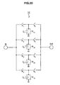
- FIG. 20 is an explanatory figure that shows a known charge domain filter circuit, proposed by Bagheri et al., that has reconfigurable filter characteristics.
- FIGS. 21A, 21B and 21C are explanatory figures that show waveforms of clock signals that are input to a charge domain filter circuit 10 in FIG. 20 .
- the clock signals shown in FIGS. 21A, 21B and 21C are respectively input to the various switches shown in the charge domain filter circuit 10 in FIG. 20 . Each switch is on when the corresponding clock signal (indicated by the characters next to the switch) is high.
- the charge domain filter circuit 10 shown in FIG. 20 is a sinc filter that is capable of switching its decimation ratio to 2 and 3.
- the charge domain filter circuit 10 shown in FIG. 20 operates such that the decimation ratio becomes 2 when the clock signals shown in FIG. 21B are input, and the decimation ratio becomes 3 when the clock signals shown in FIG. 21C are input.
- the charge domain filter circuit 10 thus has reconfigurable filter characteristics.
- the operation of the charges domain filter circuit 10 will be explained.
- Four capacitors in the charge domain filter circuit 10 accumulate and discharge charges in temporal order. Taking a capacitor C 1 as an example, when a clock signal ⁇ 1,r becomes high, the two terminals of the capacitor C 1 are short-circuited and the charge is reset. When a clock signal ⁇ 1 becomes high, a charge is accumulated from the input terminal. When a clock signal K 1 becomes high, the charge is discharged from the capacitor C 1 to the output terminal.
- the clock signals shown in FIGS. 21A to 21C that are input to the charge domain filter circuit 10 have a completely different waveform from the signals in FIGS. 21B and 21C .
- the clock signal in FIG. 21C has a longer cycle.
- a read only memory (ROM) or a logic circuit such as a multi-stage shift register or the like is therefore necessary in order to generate this sort of clock signal.
- ROM read only memory
- a logic circuit such as a multi-stage shift register or the like is therefore necessary in order to generate this sort of clock signal.
- an increase in the amount of electric current consumed in the logic circuit leads to an increase in the amount of electric power consumed.
- the cycle of the clock signal is long, the low-frequency spectrum is included in the signal, which tends to cause a problem in which the clock signal spectrum is mixed into the passband of the charge domain filter, impeding reception when the charge domain filter circuit is used in a receiver.
- the present invention addresses these issues and provides a charge domain filter circuit that is new and improved, has reconfigurable filter characteristics, and is capable of operating with low power consumption.
- a charge domain filter circuit that includes a first signal output portion, a second signal output portion, and an adder portion.
- the first signal output portion outputs a first signal that is sampled at a specified time interval.
- the second signal output portion outputs a second signal that is sampled at the same time interval as the first signal and at a different time.
- the adder portion adds the first signal and the second signal together and outputs the result.
- the second signal output portion is capable of selecting the time to sample the second signal from among a plurality of times.
- the first signal output portion outputs the first signal that is sampled at the specified time interval
- the second signal output portion outputs the second signal that is sampled at the same time interval as the first signal and at the different time
- the adder portion adds together the first signal that is output by the first signal output portion and the second signal that is output by the second signal output portion and outputs the result.
- the second signal output portion is capable of selecting the time to sample the second signal from among a plurality of times. This makes it possible to provide a charge domain filter circuit that is capable of operating with low power consumption and in which the frequency characteristics can be reconfigured by selecting the time to sample the second signal from among the plurality of times.
- the charge domain circuit may also include a clock signal generation portion that generates a plurality of clock signals that are input to the second signal output portion.
- the second signal output portion may be capable of selecting the time to sample the second signal by selecting and inputting one of the clock signals that is generated by the clock signal generation portion. This makes it possible to provide a charge domain filter circuit that is capable of selecting the time to sample the second signal by switching the clock signal that is input to the second signal output portion, and thus is capable of changing the frequency characteristics by switching the clock signal.
- the specified time interval may also be variable. Varying the time interval at which the sampling is performed makes it possible to vary the frequency characteristics.
- a charge domain filter circuit can be provided that is new and improved, that is capable of operating with low power consumption, and in which the frequency characteristics can be reconfigured.
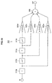
- FIG. 1 is an explanatory figure that uses a block diagram to explain a configuration of a charge domain filter circuit 100 according to the first embodiment of the present invention.
- the charge domain filter circuit 100 according to the first embodiment of the present invention will be explained below using FIG. 1 .
- the charge domain filter circuit 100 is an example of a finite impulse response (FIR) filter and is configured such that it includes delay registers 110a, 110b, 110c, 110d, 110e, 110f, switches S1, S2, S3, S4, S5, multipliers 120a, 120b, and an adder 130.
- FIR finite impulse response
- a discrete-time signal that is sampled from a continuous-time signal at a sampling interval T is input from an input terminal IN to the charge domain filter circuit 100.
- the sampling frequency is expressed as f s (1/T).
- the delay registers 110a, 110b, 110c, 110d, 110e, 110f each output the sampled input signal after delaying for the time T from the time when the input signal was sampled.
- the output from the delay register 110a is input to the multiplier 120a. Only one of the outputs from the delay registers 110b to 110f is selected, as described later, and is input to the multiplier 120b.
- the sampling interval T is a variable value that can be set as desired.
- the sampling interval T may also be varied in order to obtain the desired frequency characteristics.
- Only one of the switches S1, S2, S3, S4, S5 is selected to change to an on state. Selecting only one of the switches S1, S2, S3, S4, S5 to change to the on state makes it possible to select only one of the outputs from the delay registers 110b to 110f to be output to the multiplier 120b.
- the multiplier 120a halves the output from the delay register 110a and outputs it.
- the multiplier 120b halves the output from the selected one of the delay registers 110b to 110f and outputs it.
- the outputs from the multipliers 120a, 120b are input to the adder 130.
- the adder 130 inputs the outputs from the multipliers 120a, 120b, adds the two inputs together, and outputs the sum.
- Equation 1 A transfer function of the charge domain filter circuit 100 configured as shown in FIG. 1 is expressed by Equation 1 below.
- the charge domain filter circuit 100 enters a state in which only the switch S3 is closed.
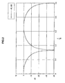
- the normalized frequency characteristics in this case are shown in FIG. 2 .
- the line indicated by dB_H(f) expresses the normalized frequency characteristics in the state in which only the switch S3 is closed.
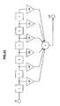
- FIG. 22 A block diagram of a sinc filter for implementing the transfer function shown by Equation 2 is shown in FIG. 22 .
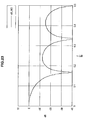
- the normalized frequency characteristics of the sinc filter shown in FIG. 22 are shown in FIG. 23 . Comparing the normalized frequency characteristics in FIG. 2 and the normalized frequency characteristics in FIG. 23 , it can be seen that both show the same frequency characteristics in the low frequency range up to the normalized frequency 0.167. However, a comparison of Equation 1 and Equation 2 shows that unlike the sinc filter transfer function shown by Equation 2, which requires that six samples with six different delay times be added together, the transfer function of the charge domain filter circuit 100 shown by Equation 1 requires only two samples to be added together. Further, in the low frequency range up to the normalized frequency 0.167, the charge domain filter circuit 100 shown in FIG. 1 has the advantage that it can achieve the same frequency characteristics as the sinc filter shown in FIG. 22 with a configuration that has fewer elements than the sinc filter shown in FIG. 22 .
- FIG. 1 the positions of the notches in the normalized frequency characteristics for the charge domain filter circuit 100 shown in FIG. 1 correspond to the zero point of the transfer function, giving the charge domain filter circuit 100 the advantage of being able to vary the positions of the notches in the normalized frequency characteristics by changing the value of n in Equation 1, that is, by turning on only one of the switches S1 to S5.
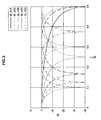
- FIG. 3 is an explanatory figure that shows how the positions of the notches in the normalized frequency characteristics in the charge domain filter circuit 100 are varied by changing the value of n.
- FIG. 3 is an explanatory figure that shows how the positions of the notches in the normalized frequency characteristics in the charge domain filter circuit 100 are varied by changing the value of n.
- the positions of the notches in the normalized frequency characteristics can be varied by changing the value of n in Equation 1, that is, by turning on only one of the switches S1 to S5.
- the charge domain filter circuit 100 according to the first embodiment of the present invention has been explained above. Next, an example of an implementation of the charge domain filter circuit 100 according to the first embodiment of the present invention will be explained.
- FIG. 4 is an explanatory figure that shows an example of a circuit in a case where the charge domain filter circuit 100 according to the first embodiment of the present invention, shown in FIG. 1 , is implemented as an actual circuit that is configured from switches and capacitors.
- the configuration of the charge domain filter circuit 100 according to the first embodiment of the present invention will be explained below with reference to FIG. 4 .
- the charge domain filter circuit 100 has an eight-tier configuration in which each tier includes six switches and two capacitors. A charge is repeatedly input to the capacitors from an input terminal IN, and a charge is repeatedly discharged from the capacitors to an output terminal OUT, by switching the switches shown in FIG. 4 as necessary.
- FIG. 5 is an explanatory figure that shows waveforms of clock signals that are input to the charge domain filter circuit 100 according to the first embodiment of the present invention that is shown in FIG. 4 .
- the intervals between the rising edges of adjacent clock signals corresponds to the sampling interval T described above.
- the clock signals ⁇ 1 to ⁇ 8 in FIG. 5 respectively correspond to the symbols ( ⁇ 1 , ⁇ 2 , ⁇ 3 , ⁇ 4 , ⁇ 5 , ⁇ 6 , ⁇ 7 , ⁇ 8 ) for various switches in FIG. 4 .
- the switches shown in FIG. 4 that correspond to the clock signal become on.
- ⁇ is used in FIG. 4 to indicate a switch that is turned on by one clock signal.
- ⁇ 1a ( ⁇ 4 , ⁇ 5 , ⁇ 6 , ⁇ 7 , ⁇ 8 ) indicates that the switch 151f becomes on when any one of the clock signals ⁇ 4 to ⁇ 8 becomes high
- ⁇ 1b ( ⁇ 3 ) indicates that the switch 151g becomes on when the clock signal ⁇ 3 becomes high.
- ⁇ 1a to ⁇ 8a indicate switches that become on when the clock signals that are shown in the corresponding positions become high.
- the switch 151f becomes on when the clock signal ⁇ 6 becomes high
- the switch 152f becomes on when the clock signal ⁇ 7 becomes high
- the switch 153f becomes on when the clock signal ⁇ 8 becomes high.
- FIG. 6 is an explanatory figure that shows a circuit that selects the clock signal that is input to the charge domain filter circuit 100 according to the first embodiment of the present invention that is shown in FIG. 4 .
- each of the switches for inputting the clock signal to the charge domain filter circuit 100 may be configured from a complementary metal oxide semiconductor (CMOS) transfer gate. Configuring each switch from a CMOS transfer gate makes it possible to align all the switches to the same delay time.
- the circuit in FIG. 6 is configured such that one of the clock signals for ⁇ 1a becomes high and the switch 151f becomes on when any one of switches S1 to S5 is turned on.
- FIG. 6 illustrates a case where the switch S3 is turned on and the clock signal ⁇ 6 becomes high.
- each of the sixteen capacitors shown in FIG. 4 it is preferable for each of the sixteen capacitors shown in FIG. 4 to have the same capacitance.
- One of a metal oxide field effect transistor (MOSFET) and a CMOSFET may also be used for each switch in the charge domain filter circuit 100 according to the first embodiment of the present invention that is shown in FIG. 4 .
- MOSFET metal oxide field effect transistor
- CMOSFET CMOSFET
- the charge domain filter circuit 100 that is shown in FIG. 4 is a filter with the same sampling rate for both input and output, making it possible to switch the notch positions of the normalized frequency characteristics in five different ways by switching the clock signals that are input.
- the configuration of the charge domain filter circuit 100 according to the first embodiment of the present invention has been explained above. Next, the operation of the charge domain filter circuit 100 according to the first embodiment of the present invention will be explained.
- the switches 151c, 151d both become off, and the switch 151e becomes on, causing the charge that is accumulated in the capacitor C 1b to be output to the output terminal OUT.
- the switch 151f becomes on, causing the charge that is accumulated in the capacitor C 1a to be output to the output terminal OUT.
- the switch 151f is turned on when the clock signal ⁇ 6 becomes high, and the charge that is accumulated in the capacitor C 1a is output to the output terminal OUT.
- the switch that becomes on only when the clock signal ⁇ 6 becomes high is the switch 154e.
- the switch 154e becomes on, the charge in the capacitor C 4b is output to the output terminal OUT.
- the charge is accumulated in the capacitor C 4b when the clock signal ⁇ 5 becomes high at a time that is equivalent to one sampling cycle prior to the time when the clock signal ⁇ 6 becomes high.
- the transfer function thus becomes the sum of the transfer function for the capacitor C 4b and the transfer function for the capacitor C 1a , as shown in Equation 3 below.
- H z z - 1 + z - 4 2
- the accumulating and discharging of the charges is repeatedly performed in the same manner in each sampling cycle, even for the capacitors C 2a , C 2b and the like, so the sampling rate is the same for both input and output.
- the circuit that is shown in FIG. 4 as the entire circuit, is equivalent to the state in which only the switch S3 is on in the charge domain filter circuit 100 shown in FIG. 1 . Therefore, in the case where only the switch S3 is on, the normalized frequency characteristics for the charge domain filter circuit 100 shown in FIG. 4 have the same properties as the normalized frequency characteristics shown in FIG. 2 .
- the operation of the charge domain filter circuit 100 according to the first embodiment of the present invention has been explained above.
- the timing of the discharging of the charges can be controlled by controlling the output of the clock signals, which makes it easy to change the frequency characteristics.
- the clock signals that are input to the charge domain filter circuit 100 are short-cycle clock signals with identical waveforms and differ only in their phases, so the clock signals are easy to generate, and the amount of electric power that is consumed can be kept low even when the circuit is operated at high speed.
- the waveforms of the clock signals that are input to the charge domain filter circuit 100 are simple, rectangular waves with short cycles, and low-frequency components are not included in the clock signal spectrum. Therefore, even if the clock signal spectrum temporarily becomes mixed into the passband of the filter, it can be easily eliminated.
- the charge domain filter circuit 100 that was explained in the first embodiment of the present invention can change the frequency characteristics by integrating two signals that are sampled at different times and switching the sampling timing of one of the signals.
- a charge domain filter circuit will be explained that can change the frequency characteristics by integrating three signals that are sampled at different times.
- FIG. 7 is an explanatory figure that uses a block diagram to explain a configuration of a charge domain filter circuit 200 according to the second embodiment of the present invention.
- the charge domain filter circuit 200 according to the second embodiment of the present invention will be explained below using FIG. 7 .
- the charge domain filter circuit 200 is an example of a FIR filter and is configured such that it includes delay registers 210a, 210b, 210c, multipliers 220a, 220b, 220c, and an adder 230.
- a discrete-time signal that is sampled from a continuous-time signal at a sampling interval T is input to the charge domain filter circuit 200 from an input terminal IN.
- the sampling frequency is expressed as f s (1/T).
- the delay register 210a outputs the sampled input signal after delaying for the time T from the time when the input signal was sampled.
- the signal that is output from the delay register 210a is input to the delay register 210b and the multiplier 220a.
- the sampling interval T is a variable value that can be set as desired.
- the sampling interval T may also be varied in order to obtain the desired frequency characteristics.
- the delay register 210b After delaying for a time n x T (n times T, where n is an integer of 1 or greater), the delay register 210b outputs the signal that was output from the delay register 210a. That is, the output signal from the delay register 210b is a signal that is delayed for T (n + 1) from the time when the signal was sampled. The output signal from the delay register 210b is input to the delay register 210c and the multiplier 220b. After delaying for an additional time n x T, the delay register 210c outputs the signal that was output from the delay register 210b. That is, the output signal from the delay register 210c is a signal that is delayed for T (2n + 1) from the time when the signal was sampled. The output signal from the delay register 210c is input to the multiplier 220c.
- the multiplier 220a multiplies the signal that was output from the delay register 210a by 1/(2 +
- the multiplier 220b multiplies the signal that was output from the delay register 210b by a/(2 +
- the multiplier 220c multiplies the signal that was output from the delay register 210c by 1/(2 +
- the adder 230 adds together the output signals from the multipliers 220a, 220b, 220c and outputs the result.
- the reason for treating the value of a as an absolute value is that a negative value can be obtained for a.
- the value of a can be made a negative value by differentiating the charge domain filter circuit 200 shown in FIG. 7 and inputting a reverse phase signal to the delay register 210b.
- ⁇ 2 ⁇ ⁇ ⁇ frel 4 ⁇ n
- frel is the relative frequency when the lowest frequency at which a notch is formed is 1.0 in a case where a is zero.
- H z z - 1 + ⁇ ⁇ z - n + 1 + z - 2 ⁇ n + 1 2 + ⁇
- Equation 5 Equation 5 above becomes Equation 6 below.
- H z z - 1 + z - 3 2
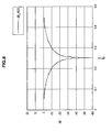
- the line indicated by dB_H3(f) in FIG. 8 indicates the frequency characteristics in this case.
- a notch forms where the normalized frequency f/f s is 0.25 (1/4).
- the output from the multiplier 220b is also zero, which makes the charge domain filter circuit 200 a charge domain filter that integrates and outputs two signals.
- the frequency at which the notch position forms is limited to a frequency at which the integer portion of the sampling frequency is 1.
- Equation 7 The transfer function for the charge domain filter circuit 200 when the value of a is 0.618 is shown in Equation 7 below.
- H z z - 1 + 0.618 ⁇ z - n + 1 + z - 2 ⁇ n + 1 2.618
- FIG. 9 The line indicated by dB_H3(f) in FIG. 9 indicates the frequency characteristics in this case. It can be seen that the position of the notch frequency (0.3) is twenty percent higher than in FIG. 8 .
- Equation 4 the value that can be obtained for a is in the range from -2 to 2. Changing the value of a within this range makes it possible to vary the notch frequency without being limited by the sampling frequency f s .
- the charge domain filter circuit 200 according to the second embodiment of the present invention has been explained above. Next, an example of a configuration of the charge domain filter circuit 200 according to the second embodiment of the present invention will be explained.
- FIG. 10 is an explanatory figure that shows an example of a circuit in a case where the charge domain filter circuit 200 according to the second embodiment of the present invention shown in FIG. 7 is implemented as an actual circuit that is configured from switches and capacitors.
- the configuration of the charge domain filter circuit 200 according to the second embodiment of the present invention will be explained below with reference to FIG. 10 .
- the charge domain filter circuit 200 that is shown in FIG. 10 is an example of a configuration in the form of an actual circuit that is configured from switches and capacitors, with the value of n in the configuration shown in FIG. 7 set to 1.
- the charge domain filter circuit 200 according to the second embodiment of the present invention has a six-tier configuration in which each tier includes twelve switches and four capacitors. A charge is repeatedly input to the capacitors from an input terminal IN, and a charge is repeatedly discharged from the capacitors to an output terminal OUT, by switching the individual switches as necessary.
- FIG. 11 is an explanatory figure that shows waveforms of clock signals that are input to the charge domain filter circuit 200 according to the second embodiment of the present invention that is shown in FIG. 10 .
- the intervals between the rising edges of adjacent clock signals corresponds to the sampling interval T described above.
- the clock signals ⁇ 1 to ⁇ 6 in FIG. 11 respectively correspond to the symbols ( ⁇ 1 , ⁇ 2 , ⁇ 3 , ⁇ 4 , ⁇ 5 , ⁇ 6 ) for various switches in FIG. 10 .
- the switches shown in FIG. 10 that correspond to the clock signal become on. Therefore, repeatedly turning the clock signals ⁇ 1 to ⁇ 6 in FIG. 11 to high and low causes charges to be accumulated in the various capacitors shown in FIG. 10 and causes the signal sampling to be performed.
- the letters A and B are also placed next to some of the switches in addition to the symbols that are used for the switches and that correspond to the clock signals.
- the label A• ⁇ 1 for the switch 251e indicates that clock gating is performed for the clock signal ⁇ 1 by a control logic A. Specifically, if the control logic A is 1, the switch 251e turns on and off according to whether the clock signal ⁇ 1 is in a high or a low state, and if the control logic A is zero, the switch 251e is off, regardless of whether the clock signal ⁇ 1 is in a high or a low state.
- the vertically aligned capacitors it is preferable for all of the vertically aligned capacitors to have the same capacitance.
- the capacitors C 1a , C 2a , C 3a , C 4a , C 5a , C 6a it is preferable for all of the capacitors C 1a , C 2a , C 3a , C 4a , C 5a , C 6a to have the same capacitance.
- the c and d capacitors within each tier the capacitors C 1c , and C 1d , the capacitors C 2c and C 2d , the capacitors C 3c and C 3d , the capacitors C 4c and C 4d , the capacitors C 5c and C 5d , and the capacitors C 6c and C 6d , to have the same capacitance.
- the value of a in Equation 5 above can be determined by normalizing the capacitances of the capacitors C 1a and C 1b by the capacitance of the capacitor C 1c .
- one of a MOSFET and a CMOSFET may be used for each switch in the charge domain filter circuit 200 according to the second embodiment of the present invention that is shown in FIG. 10 .
- the charge domain filter circuit 200 that is shown in FIG. 10 is a filter with the same sampling rate for both input and output.
- the charge domain filter circuit 200 is also capable of switching the notch positions of the normalized frequency characteristics according to the capacitances of the capacitors and the states of the control logics A, B.
- the configuration of the charge domain filter circuit 200 according to the second embodiment of the present invention has been explained above. Next, the operation of the charge domain filter circuit 200 according to the second embodiment of the present invention will be explained.
- the accumulating and discharging of the charges is repeatedly performed in the same manner in each sampling cycle, even for the capacitors in the other tiers, so the sampling rate is the same for both input and output.
- the capacitance ratios of the capacitors in each of the tiers will be explained using a.
- the ratio of the sum of the capacitances of the capacitors C 1a and C 1b to the capacitance of the capacitor C 1c may be a:1.
- the ratio of the sum of the capacitances of the capacitors C 1a and C 1b to the capacitance of the capacitor C 1c to the capacitance of the capacitor C 1d is a:1:1. Therefore, if the capacitance of the capacitor C 1c is 1, the total of the capacitances of the capacitors in all of the tiers is 2 + a, so it can be used for the denominator in Equation 5 shown above.
- the first term in the numerator of Equation 5 represents a delay of one cycle from the sampling time
- the second term in the numerator represents a delay of two cycles
- the third term in the numerator represents a delay of three cycles. Therefore, the first term in the numerator of Equation 5 corresponds to the output of the charge that was stored in the capacitor C 2c
- the second term in the numerator corresponds to the charges that were stored in the capacitors C 1a and C 1b
- the third term in the numerator corresponds to the output of the charge that was stored in the capacitor C 6d .
- Equation 5 the charge domain filter circuit 200 that is shown in FIG. 10 satisfies Equation 5 and that the charge domain filter circuit 200 that is shown in FIG. 7 can be implemented by the circuit configuration that is shown in FIG. 10 .
- Equation 5 the value of a in Equation 5 is determined by the ratio of the sum of the capacitances of the capacitors C 1a and C 1b to the capacitance of the capacitor C 1c .
- the capacitances of the capacitors C 1a , C 1b are binary-weighted such that the capacitance ratio of the capacitor C 1a to capacitors C 1c is 0.5:1 and the capacitance ratio of the capacitor C 1b to capacitor C 1c is 1:1.
- the capacitance of the capacitor C 1c is 1
- the sum of the capacitances of the capacitors C 1a and C 1b (that is, the value of a in Equation 5) can be set to any one of the four values of 0, 0.5, 1, and 1.5 by changing the states of the control logics A, B.
- the value of a in Equation 5 can also be varied continuously by using variable capacitors whose capacitances can be continuously varied, instead of the capacitors C 1a and C 1b . Using the variable capacitors makes it possible to continuously vary the normalized frequency characteristics.
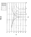
- FIG. 12 is an explanatory figure that shows the normalized frequency characteristics of the charge domain filter circuit 200 according to the second embodiment of the present invention in a case where the value of a is varied among the four values of 0, 0.5, 1, and 1.5.
- dB_HO(f) shows the normalized frequency characteristics when the value of a is 0
- dB_H1(f) shows the normalized frequency characteristics when the value of a is 0.5
- dB_H2(f) shows the normalized frequency characteristics when the value of a is 1
- dB_H3(f) shows the normalized frequency characteristics when the value of a is 1.5.
- a reverse phase signal may be input to the series of capacitors from the capacitors C 1a and C 1b to the capacitors C 6a and C 6b by differentiating the charge domain filter circuit 200.
- Inputting the reverse phase signal to the series of capacitors from the capacitors C 1a and C 1b to the capacitors C 6a and C 6b causes the value of a to become negative, making it possible to configure the charge domain filter circuit 200 such that it satisfies the transfer function shown in Equation 5.
- the clock signals that are input to the charge domain filter circuit 200 are short-cycle clock signals with identical waveforms and differ only in their phases, so the clock signals are easy to generate, and the amount of electric power that is consumed can be kept low even when the circuit is operated at high speed.
- the waveforms of the clock signals that are input to the charge domain filter circuit 200 are simple, rectangular waves with short cycles, and low-frequency components are not included in the clock signal spectrum. Therefore, even if the clock signal spectrum temporarily becomes mixed into the passband of the filter, it can be easily eliminated.
- the charge domain filter circuit 200 that was explained in the second embodiment of the present invention can change the frequency characteristics by integrating three signals that are sampled at different times.
- a charge domain filter circuit will be explained that can change the frequency characteristics by integrating four signals that are sampled at different times.
- FIG. 13 is an explanatory figure that uses a block diagram to explain a configuration of a charge domain filter circuit 300 according to the third embodiment of the present invention.
- the charge domain filter circuit 300 according to the third embodiment of the present invention will be explained below using FIG. 13 .
- the charge domain filter circuit 300 is an example of a FIR filter and is configured such that it includes delay registers 310a, 310b, 310c, 310d, multipliers 320a, 320b, 320c, 320d, and an adder 330.
- a discrete-time signal that is sampled from a continuous-time signal at a sampling interval T is input to the charge domain filter circuit 300 from an input terminal IN.
- the sampling frequency is expressed as f s (1/T).
- the delay register 310a outputs the sampled input signal after delaying for the time T from the time when the input signal was sampled.
- the signal that is output from the delay register 310a is input to the delay register 310b and the multiplier 320a.
- the sampling interval T is a variable value that can be set as desired.
- the sampling interval T may also be varied in order to obtain the desired frequency characteristics.
- the delay register 310b After delaying for a time n x T (n times T, where n is an integer of 1 or greater), the delay register 310b outputs the signal that was output from the delay register 310a. That is, the output signal from the delay register 310b is a signal that is delayed for T (n + 1) from the time when the signal was sampled. The output signal from the delay register 310b is input to the delay register 310c and the multiplier 320b.
- the delay register 310c After delaying for an additional time T, the delay register 310c outputs the signal that was output from the delay register 310b. That is, the output signal from the delay register 310c is a signal that is delayed for T (n + 2) from the time when the signal was sampled. The output signal from the delay register 310c is input to the delay register 310d and the multiplier 320c. After delaying for a time n x T, the delay register 310d outputs the signal that was output from the delay register 310c. That is, the output signal from the delay register 310d is a signal that is delayed for T (2n + 2) from the time when the signal was sampled. The output signal from the delay register 310d is input to the multiplier 320d.
- the multiplier 320a multiplies the signal that was output from the delay register 310a by 1/(2 +
- the multiplier 320b multiplies the signal that was output from the delay register 310b by a/(2 +
- the multiplier 320c also multiplies the signal that was output from the delay register 310c by a/(2 +
- the multiplier 320d multiplies the signal that was output from the delay register 310d by 1/(2 +
- the adder 330 adds together the output signals from the multipliers 320a, 320b, 320c, 320d and outputs the result.
- the reason for treating the value of a as an absolute value is that a negative value can be obtained for a, in the same manner as in the second embodiment. Specifically, the value of a can be made a negative value by differentiating the circuit and inputting a reverse phase signal to the delay registers 310b, 310d.
- Equation 9 Equation 9 above becomes Equation 10 below.
- H z z - 1 + z - 4 2
- the frequency characteristics as normalized by the sampling frequency f s in this case are shown in FIG. 14 .
- a notch forms where the normalized frequency f/f s is 0.167 (1/6).
- the outputs from the multiplier 320b, 320c are also zero, which makes the charge domain filter circuit 300 a charge domain filter that integrates and outputs two signals.
- the frequency at which the notch position forms is limited to a frequency at which the integer portion of the sampling frequency is 1.
- Equation 11 The transfer function for the charge domain filter circuit 300 when the value of a is 0.382 is shown in Equation 11 below.
- H z z - 1 + 0.382 ⁇ z - n + 1 + 0.382 ⁇ z - n + 2 + z - 2 ⁇ n + 2 2.764
- the frequency characteristics as normalized by the sampling frequency f s are shown in FIG. 15 .
- the line indicated by dB_H4(f) in the graph shown in FIG. 15 indicates the normalized frequency characteristics in this case. It can be seen that the position of the notch frequency (0.2) is twenty percent higher than in FIG. 14 .
- the charge domain filter circuit 300 according to the third embodiment of the present invention has been explained above.
- the frequency characteristics of the charge domain filter circuit 300 can be changed by integrating the four signals that are sampled at different times and varying the sampling timing such that the value of a is varied.
- a charge domain filter circuit according to a fourth embodiment of the present invention will be explained.
- the fourth embodiment of the present invention that is explained below varies the frequency characteristics by combining two of the charge domain filter circuits shown in the second embodiment of the present invention.
- FIG. 16 is an explanatory figure that shows a charge domain filter circuit 400 according to the fourth embodiment of the present invention.
- FIG. 17 is an explanatory figure that shows an example of a circuit in a case where the charge domain filter circuit 400 according to the fourth embodiment of the present invention shown in FIG. 16 is implemented as an actual circuit. The configuration of the charge domain filter circuit 400 will be explained below with reference to FIGS. 16 and 17 .
- the charge domain filter circuit 400 which is an example of the fourth embodiment of the present invention, is configured such that it includes delay registers 410a, 410b, 410c, 410d, 410e, multipliers 420a, 420b, 440a, 440b, and adders 430a, 430b.
- a discrete-time signal that is sampled from a continuous-time signal at a sampling interval T is input from an input terminal IN to the charge domain filter circuit 400 shown in FIG. 16 .
- the sampling frequency is expressed as f s (1/T).
- the delay registers 410a, 410b, 410c, 410d, 410e each output the input signal after delaying for the time T.
- the sampling interval T is a variable value that can be set as desired.
- the sampling interval T may also be varied in order to obtain the desired frequency characteristics.
- the multipliers 420a, 420b each multiply the signal that is output from the delay register 410c by the coefficient a and output the results.
- the adder 430a adds together the outputs from the delay register 410a, the multiplier 420a, and the delay register 410e and outputs the result.
- the adder 430b adds together the outputs from the delay registers 410b, the multiplier 420b, and the delay register 410d and outputs the result.
- the multipliers 440a, 440b respectively multiply the signals that are output from the adders 430a, 430b by 1/(2 +
- the charge domain filter circuit 400 that is shown in FIG. 16 can be made to correspond to the charge domain filter circuit 200 according to the second embodiment of the present invention that is shown in FIG. 7 in the cases where the value of n is set to 1 and to 2.
- FIG. 17 is an explanatory figure that shows an example of a circuit in the case where the charge domain filter circuit 400 according to the fourth embodiment of the present invention shown in FIG. 16 is implemented as an actual circuit that is configured from switches and capacitors.
- the charge domain filter circuit 400 according to the fourth embodiment of the present invention has an eight-tier configuration in which each tier is configured from a grouping of twelve switches and four capacitors. A charge is repeatedly input to the capacitors from an input terminal IN, and a charge is repeatedly discharged from the capacitors to an output terminal OUT, by switching the individual switches as necessary.
- FIG. 18 is an explanatory figure that shows waveforms of clock signals that are input to the charge domain filter circuit 400 according to the fourth embodiment of the present invention that is shown in FIG. 17 .
- the intervals between the rising edges of adjacent clock signals corresponds to the sampling interval T described above.
- the clock signals ⁇ 1 to ⁇ 8 in FIG. 18 respectively correspond to the symbols ( ⁇ 1 , ⁇ 2 , ⁇ 3 , ⁇ 4 , ⁇ 5 , ⁇ 6 , ⁇ 7 , ⁇ 8 ) for various switches in FIG. 17 .
- the switches shown in FIG. 17 that correspond to the clock signal become on. Therefore, repeatedly turning the clock signals ⁇ 1 to ⁇ 8 in FIG. 18 to high and low causes charges to be accumulated in the various capacitors shown in FIG. 17 and causes the signal sampling to be performed.
- the letters A and B are also placed next to some of the switches in addition to the symbols that are used for the switches and that correspond to the clock signals.
- the label A• ⁇ 1 for the switch 451e indicates that clock gating is performed for the clock signal ⁇ 1 by a control logic A. Specifically, if the control logic A is 1, the switch 451e turns on and off according to whether the clock signal ⁇ 1 is in a high or a low state, and if the control logic A is zero, the switch 451e is off, regardless of whether the clock signal ⁇ 1 is in a high or a low state.
- the symbol ⁇ is used in FIG. 17 to indicate a switch that is turned on by one clock signal.
- ⁇ 1c ( ⁇ 3 , ⁇ 2 ) indicates that the switch 451k becomes on when either one of the clock signals ⁇ 2 , ⁇ 3 becomes high.
- ⁇ 1c to ⁇ 8c and ⁇ 1d to ⁇ 8d indicate switches that become on when the clock signals that are shown in the corresponding positions become high.
- the switch 451k becomes on when the clock signal ⁇ 3 becomes high
- the switch 4511 becomes on when the clock signal ⁇ 5 becomes high
- the switch 452k becomes on when the clock signal ⁇ 4 becomes high
- the switch 4521 becomes on when the clock signal ⁇ 6 becomes high.
- the vertically aligned capacitors it is preferable for all of the vertically aligned capacitors to have the same capacitance, in the same manner as in the charge domain filter circuit 200 according to the second embodiment of the present invention shown in FIG. 10 .
- the capacitors C 1c and C 1d , the capacitors C 2c and C 2d , the capacitors C 3c and C 3d , the capacitors C 4c and C 4d , the capacitors C 5c and C 5d , and the capacitors C 6c and C 6d to have the same capacitance, in the same manner as in the charge domain filter circuit 200 according to the second embodiment of the present invention shown in FIG. 10 .
- the value of a in Equation 5 above can be determined by normalizing the capacitances of the capacitors C 1a and C 1b by the capacitance of the capacitor C 1c .
- One of a MOSFET and a CMOSFET may be used for each switch in the charge domain filter circuit 400 according to the fourth embodiment of the present invention that is shown in FIG. 17 .
- the charge domain filter circuit 400 that is shown in FIG. 17 is a filter with the same sampling rate for both input and output, making it possible to switch the notch positions of the normalized frequency characteristics in eight different ways.
- the configuration of the charge domain filter circuit 400 according to the fourth embodiment of the present invention has been explained above. Next, the operation of the charge domain filter circuit 400 according to the fourth embodiment of the present invention will be explained.
- the accumulating and discharging of the charges is repeatedly performed in the same manner in each sampling cycle, even for the capacitors in the other tiers, so the sampling rate is the same for both input and output.
- the capacitance ratios of the capacitors in each of the tiers will be explained using a.
- the ratio of the sum of the capacitances of the capacitors C 1a and C 1b to the capacitance of the capacitor C 1c may be a:1.
- the ratio of the sum of the capacitances of the capacitors C 1a and C 1b to the capacitance of the capacitor C 1c to the capacitance of the capacitor C 1d is a:1:1. Therefore, if the capacitance of the capacitor C 1c is 1, the total of the capacitances of the capacitors in all of the tiers is 2 + a, so it can be used for the denominator in Equation 5 shown above.
- the first term in the numerator of Equation 5 represents a delay of one cycle from the sampling time
- the second term in the numerator represents a delay of two cycles
- the third term in the numerator represents a delay of three cycles. Therefore, the first term in the numerator of Equation 5 corresponds to the output of the charge that was stored in the capacitor C 2c
- the second term in the numerator corresponds to the charges that were stored in the capacitors C 1a and C 1b
- the third term in the numerator corresponds to the output of the charge that was stored in the capacitor C 8d .
- Equation 12 all of the sampling times are delayed by one cycle more than when 1 is substituted for n in Equation 5, but because the delay is one cycle for all of the sampling times, there is absolutely no effect on the frequency characteristics.
- switches 458i, 458j, 4561 Other switches that also become on when the clock signal ⁇ 3 becomes high are the switches 458i, 458j, 4561. Accordingly, when the clock signal ⁇ 3 becomes high, the charges that are stored in the capacitors C 8a , C 8b , C 6d are also output to the output terminal OUT. The charges that are stored in the capacitors C 8a , C 8b were accumulated when the clock signal ⁇ 8 became high, three sampling cycles before the clock signal ⁇ 3 . The charge that is stored in the capacitor C 6d was accumulated when the clock signal ⁇ 6 became high, five sampling cycles before the clock signal ⁇ 3 .
- the capacitance ratios of the capacitors in each of the tiers will be explained using a.
- the ratio of the sum of the capacitances of the capacitors C 1a and C 1b to the capacitance of the capacitor C 1c may be a:1.
- the ratio of the sum of the capacitances of the capacitors C 1a and C 1b to the capacitance of the capacitor C 1c to the capacitance of the capacitor C 1d is a:1:1.
- the first term in the numerator of Equation 5 represents a delay of one cycle from the sampling time
- the second term in the numerator represents a delay of three cycles
- the third term in the numerator represents a delay of five cycles. Therefore, the first term in the numerator of Equation 5 corresponds to the output of the charge that was stored in the capacitor C 2c
- the second term in the numerator corresponds to the charges that were stored in the capacitors C 8a and C 8b
- the third term in the numerator corresponds to the output of the charge that was stored in the capacitor C 6d .
- Equation 12 and Equation 13 the value of a in Equation 12 and Equation 13 is determined by the ratio of the sum of the capacitances of the capacitors C 1a and C 1b to the capacitance of the capacitor C 1c , in the same manner as the value of a in Equation 5.
- the capacitances of the capacitors C 1a , C 1b are binary-weighted such that the capacitance ratio of the capacitor C 1a to capacitor C 1c is 0.5:1 and the capacitance ratio of the capacitor C 1b to capacitor C 1c is 1:1.
- the sum of the capacitances of the capacitors C 1a and C 1b (that is, the value of a in Equation 12 and Equation 13) can be set to any one of the four values of 0, 0.5, 1, and 1.5 by changing the states of the control logics A, B.
- the value of a in Equation 12 and Equation 13 can also be varied continuously by using variable capacitors whose capacitances can be continuously varied, instead of the capacitors C 1a and C 1b . Using the variable capacitors makes it possible to continuously vary the normalized frequency characteristics.
- FIG. 19 is an explanatory figure that shows the normalized frequency characteristics of the charge domain filter circuit 400 according to the fourth embodiment of the present invention in a case where the value of a is varied among the four values of 0, 0.5, 1, and 1.5.
- FIG. 19 is an explanatory figure that shows the normalized frequency characteristics of the charge domain filter circuit 400 according to the fourth embodiment of the present invention in a case where the value of a is varied among the four values of 0, 0.5, 1, and 1.5.
- dB_H4(f) shows the normalized frequency characteristics when the value of a is 0
- dB_H5(f) shows the normalized frequency characteristics when the value of a is 0.5
- dB_H6(f) shows the normalized frequency characteristics when the value of a is 1
- dB_H7(f) shows the normalized frequency characteristics when the value of a is 1.5.
- FIG. 19 it is possible to achieve normalized frequency characteristics with different positions for the notch frequencies by varying the value of a.
- changing the value of n changes the order of the filter and changes the notch frequency significantly.
- a reverse phase signal may be input to the series of capacitors from the capacitors C 1a and C 1b to the capacitors C 8a and C 8b by differentiating the charge domain filter circuit 400.
- Inputting the reverse phase signal to the series of capacitors from the capacitors C 1a and C 1b to the capacitors C 8a and C 8b causes the value of a to become negative, making it possible to configure the charge domain filter circuit 400 such that it satisfies the transfer functions shown in Equation 12 and Equation 13.
- the charge domain filter circuit 400 according to the fourth embodiment of the present invention, varying the value of a in Equation 12 and Equation 13 by switching the capacitances of the capacitors makes it possible to set the positions of the notch frequencies without being limited to frequencies at which the integer portion of the sampling frequency is 1, as is the case in the first embodiment of the present invention.
- the clock signals that are input to the charge domain filter circuit 400 are short-cycle clock signals with identical waveforms and differ only in their phases, so the clock signals are easy to generate, and the amount of electric power that is consumed can be kept low even when the circuit is operated at high speed.
- the waveforms of the clock signals that are input to the charge domain filter circuit 400 are simple, rectangular waves with short cycles, and low-frequency components are not included in the clock signal spectrum. Therefore, even if the clock signal spectrum temporarily becomes mixed into the passband of the filter, it can be easily eliminated.
Landscapes
- Engineering & Computer Science (AREA)
- Power Engineering (AREA)
- Filters That Use Time-Delay Elements (AREA)
Abstract
Description
- The present invention contains subjected matter related to Japanese Patent Application
JP 2007-304984 - The present invention relates to a charge domain filter circuit.
- The miniaturization of the complementary metal oxide semiconductor (CMOS) process has the disadvantage that using known circuit technology to implement the RF circuit to reduce the power supply voltage reduces the dynamic range of the signal amplitude, because there is little voltage allowance. On the other hand, because miniaturization raises the cutoff frequency of the transistor, it is suitable for operations such as high-speed switching that must be performed with precise timing. Another advantage is that, because the lithography is performed with high precision, the capacitance ratios of capacitors can be specified accurately.
- Digital RF technology is a technology that resolves the disadvantages that the miniaturization of the CMOS process engenders for the RF circuit and converts them to advantages. The main circuit in a discrete time receiver (DTR), in which digital RF technology is used for the receiver, is a charge domain filter. The charge domain filter includes a capacitor that accumulates and discharges a charge on a specified cycle. In the charge domain filter circuit, the filter is configured from only a transconductor and a switch, so it is capable of directly sampling and filtering RF signals in the gigahertz band.
- It has been proposed that the filter characteristics of the charge domain filter can be made reconfigurable by varying the frequencies and waveforms of the filter's clock signals (refer to R. Bagheri et al., "An 800 MHz to 5 GHz Software-Defined Radio Receiver in 90 nm CMOS," in IEEE Int. Solid State Circuits Conf. Dig. Tech. Papers, Feb. 2006, pp.480-481).
FIG. 20 is an explanatory figure that shows a known charge domain filter circuit, proposed by Bagheri et al., that has reconfigurable filter characteristics.FIGS. 21A, 21B and 21C are explanatory figures that show waveforms of clock signals that are input to a chargedomain filter circuit 10 inFIG. 20 . The clock signals shown inFIGS. 21A, 21B and 21C are respectively input to the various switches shown in the chargedomain filter circuit 10 inFIG. 20 . Each switch is on when the corresponding clock signal (indicated by the characters next to the switch) is high. - The charge
domain filter circuit 10 shown inFIG. 20 is a sinc filter that is capable of switching its decimation ratio to 2 and 3. The chargedomain filter circuit 10 shown inFIG. 20 operates such that the decimation ratio becomes 2 when the clock signals shown inFIG. 21B are input, and the decimation ratio becomes 3 when the clock signals shown inFIG. 21C are input. The chargedomain filter circuit 10 thus has reconfigurable filter characteristics. - The operation of the charges
domain filter circuit 10 will be explained. Four capacitors in the chargedomain filter circuit 10 accumulate and discharge charges in temporal order. Taking a capacitor C1as an example, when a clock signal Ψ1,r becomes high, the two terminals of the capacitor C1are short-circuited and the charge is reset. When a clock signal Ψ1 becomes high, a charge is accumulated from the input terminal. When a clock signal K1 becomes high, the charge is discharged from the capacitor C1 to the output terminal. - In a case where the decimation ratio is 2, an operation is repeated in which the charges of capacitors C1 and C2 are discharged simultaneously by clock signals K1 and K2, and the charges of capacitors C3 and C4 are discharged simultaneously by clock signals K3 and K4. The clock signals K1 to K4 therefore become repetitions of simple rectangular waves, as shown in
FIG. 21B . - In contrast, in a case where the decimation ratio is 3, when the clock signal Ψ1 becomes high, the charges of the capacitors C2, C3, and C4 are discharged simultaneously by clock signals K2, K3, and K4. When a clock signal W4 becomes high, the charges of the capacitors C1, C2, and C3 are discharged simultaneously by clock signals K1, K2, and K3. When a clock signal W3 becomes high, the charges of the capacitors C1, C2, and C4 are discharged simultaneously by clock signals K1, K2, and K4. When a clock signal Ψ2 becomes high, the charges of the capacitors C1, C3, and C4 are discharged simultaneously by clock signals K1, K3, and K4. The clock signals K1 to K4 therefore become repetitions of irregular rectangular waves with long cycles, as shown in
FIG. 21C . - The clock signals shown in
FIGS. 21A to 21C that are input to the chargedomain filter circuit 10 have a completely different waveform from the signals inFIGS. 21B and 21C . In particular, the clock signal inFIG. 21C has a longer cycle. A read only memory (ROM) or a logic circuit such as a multi-stage shift register or the like is therefore necessary in order to generate this sort of clock signal. For example, in a case where the clock signal is operated at a high speed on the order of gigahertz, an increase in the amount of electric current consumed in the logic circuit leads to an increase in the amount of electric power consumed. Further, if the cycle of the clock signal is long, the low-frequency spectrum is included in the signal, which tends to cause a problem in which the clock signal spectrum is mixed into the passband of the charge domain filter, impeding reception when the charge domain filter circuit is used in a receiver. - The present invention addresses these issues and provides a charge domain filter circuit that is new and improved, has reconfigurable filter characteristics, and is capable of operating with low power consumption.
- In order to address the issues described above, according to an embodiment of the present invention, there is provided a charge domain filter circuit that includes a first signal output portion, a second signal output portion, and an adder portion. The first signal output portion outputs a first signal that is sampled at a specified time interval. The second signal output portion outputs a second signal that is sampled at the same time interval as the first signal and at a different time. The adder portion adds the first signal and the second signal together and outputs the result. The second signal output portion is capable of selecting the time to sample the second signal from among a plurality of times.
- According to this configuration, the first signal output portion outputs the first signal that is sampled at the specified time interval, the second signal output portion outputs the second signal that is sampled at the same time interval as the first signal and at the different time, and the adder portion adds together the first signal that is output by the first signal output portion and the second signal that is output by the second signal output portion and outputs the result. In addition, the second signal output portion is capable of selecting the time to sample the second signal from among a plurality of times. This makes it possible to provide a charge domain filter circuit that is capable of operating with low power consumption and in which the frequency characteristics can be reconfigured by selecting the time to sample the second signal from among the plurality of times.
- The charge domain circuit may also include a clock signal generation portion that generates a plurality of clock signals that are input to the second signal output portion. The second signal output portion may be capable of selecting the time to sample the second signal by selecting and inputting one of the clock signals that is generated by the clock signal generation portion. This makes it possible to provide a charge domain filter circuit that is capable of selecting the time to sample the second signal by switching the clock signal that is input to the second signal output portion, and thus is capable of changing the frequency characteristics by switching the clock signal.
- The specified time interval may also be variable. Varying the time interval at which the sampling is performed makes it possible to vary the frequency characteristics.
- According to the embodiments of the present invention described above, a charge domain filter circuit can be provided that is new and improved, that is capable of operating with low power consumption, and in which the frequency characteristics can be reconfigured.
-
-
FIG. 1 is an explanatory figure that shows a configuration of a chargedomain filter circuit 100 according to a first embodiment of the present invention; -
FIG. 2 is an explanatory figure that shows normalized frequency characteristics in a case where only a switch S3 is closed in the chargedomain filter circuit 100 shown inFIG. 1 ; -
FIG. 3 is an explanatory figure that shows changes of positions of notches in the normalized frequency characteristics in the chargedomain filter circuit 100; -
FIG. 4 is an explanatory figure that shows an example of a circuit in a case where the chargedomain filter circuit 100 according to the first embodiment of the present invention is implemented as an actual circuit; -
FIG. 5 is an explanatory figure that shows waveforms of clock signals that are input to the chargedomain filter circuit 100 according to the first embodiment of the present invention that is shown inFIG. 4 ; -
FIG. 6 is an explanatory figure that shows a circuit that selects the clock signal that is input to the chargedomain filter circuit 100 according to the first embodiment of the present invention that is shown inFIG. 4 ; -
FIG. 7 is an explanatory figure that shows a configuration of a chargedomain filter circuit 200 according to a second embodiment of the present invention; -
FIG. 8 is an explanatory figure that shows an example of normalized frequency characteristics of the chargedomain filter circuit 200 shown inFIG. 7 ; -
FIG. 9 is an explanatory figure that shows another example of the normalized frequency characteristics of the chargedomain filter circuit 200 shown inFIG. 7 ; -
FIG. 10 is an explanatory figure that shows an example of a circuit in a case where the chargedomain filter circuit 200 according to the second embodiment of the present invention is implemented as an actual circuit; -
FIG. 1 is an explanatory figure that shows waveforms of clock signals that are input to the chargedomain filter circuit 200 according to the second embodiment of the present invention, shown inFIG. 10 ; -
FIG. 12 is an explanatory figure that shows the normalized frequency characteristics of the chargedomain filter circuit 200 according to the second embodiment of the present invention; -
FIG. 13 is an explanatory figure that shows a configuration of a chargedomain filter circuit 300 according to a third embodiment of the present invention; -
FIG. 14 is an explanatory figure that shows an example of normalized frequency characteristics of the chargedomain filter circuit 300 shown inFIG. 13 ; -
FIG. 15 is an explanatory figure that shows another example of the normalized frequency characteristics of the chargedomain filter circuit 300 shown inFIG. 13 ; -
FIG. 16 is an explanatory figure that shows a configuration of a chargedomain filter circuit 400 according to a fourth embodiment of the present invention; -
FIG. 17 is an explanatory figure that shows an example of a circuit in a case where the chargedomain filter circuit 400 according to the fourth embodiment of the present invention is implemented as an actual circuit; -
FIG. 18 is an explanatory figure that shows waveforms of clock signals that are input to the chargedomain filter circuit 400 according to the fourth embodiment of the present invention, shown inFIG. 17 ; -
FIG. 19 is an explanatory figure that shows normalized frequency characteristics of the chargedomain filter circuit 400 according to the fourth embodiment of the present invention; -
FIG. 20 is an explanatory figure that shows a known charge domain filter circuit that has reconfigurable filter characteristics; -
FIG. 21A is an explanatory figure that shows waveforms of clock signals that are input to a chargedomain filter circuit 10 inFIG. 20 ; -
FIG. 21B is an explanatory figure that shows waveforms of clock signals that are input to a chargedomain filter circuit 10 inFIG. 20 ; -
FIG. 21C is an explanatory figure that shows waveforms of clock signals that are input to a chargedomain filter circuit 10 inFIG. 20 ; -
FIG. 22 is an explanatory figure that shows a block diagram of a sinc filter for implementing a transfer function shown byEquation 2; and -
FIG. 23 is an explanatory figure that shows normalized frequency characteristics of the sinc filter shown inFIG. 22 . - Hereinafter, preferred embodiments of the present invention will be described in detail with reference to the appended drawings. Note that, in this specification and the appended drawings, structural elements that have substantially the same function and structure are denoted with the same reference numerals, and repeated explanation of these structural elements is omitted.
- First Embodiment
First, a charge domain filter circuit according to a first embodiment of the present invention will be explained.FIG. 1 is an explanatory figure that uses a block diagram to explain a configuration of a chargedomain filter circuit 100 according to the first embodiment of the present invention. The chargedomain filter circuit 100 according to the first embodiment of the present invention will be explained below usingFIG. 1 . - As shown in
FIG. 1 , the chargedomain filter circuit 100 according to the first embodiment of the present invention is an example of a finite impulse response (FIR) filter and is configured such that it includesdelay registers multipliers adder 130. - A discrete-time signal that is sampled from a continuous-time signal at a sampling interval T is input from an input terminal IN to the charge
domain filter circuit 100. The sampling frequency is expressed as fs (1/T). The delay registers 110a, 110b, 110c, 110d, 110e, 110f each output the sampled input signal after delaying for the time T from the time when the input signal was sampled. The output from thedelay register 110a is input to themultiplier 120a. Only one of the outputs from the delay registers 110b to 110f is selected, as described later, and is input to themultiplier 120b. Note that the sampling interval T is a variable value that can be set as desired. The sampling interval T may also be varied in order to obtain the desired frequency characteristics. - Only one of the switches S1, S2, S3, S4, S5 is selected to change to an on state. Selecting only one of the switches S1, S2, S3, S4, S5 to change to the on state makes it possible to select only one of the outputs from the delay registers 110b to 110f to be output to the
multiplier 120b. - The
multiplier 120a halves the output from thedelay register 110a and outputs it. Themultiplier 120b halves the output from the selected one of the delay registers 110b to 110f and outputs it. The outputs from themultipliers adder 130. Theadder 130 inputs the outputs from themultipliers - A transfer function of the charge
domain filter circuit 100 configured as shown inFIG. 1 is expressed byEquation 1 below.
(Note that n = 2, 3, 4, 5, 6.) - For example, in a case where n = 4, the charge
domain filter circuit 100 enters a state in which only the switch S3 is closed. The normalized frequency characteristics in this case are shown inFIG. 2 . In the graph shown inFIG. 2 , the line indicated by dB_H(f) expresses the normalized frequency characteristics in the state in which only the switch S3 is closed. As shown inFIG. 2 , in the case where n = 4, it can be seen that notches form at the positions where the normalized frequency f/fs, which is the signal frequency f divided by the sampling frequency fs, is 0.167 (1/6) and 0.5. - In a case where a sinc filter is used and a notch forms at the position where the normalized frequency is 1/6, a transfer function such as that in
Equation 2 is required.
- A block diagram of a sinc filter for implementing the transfer function shown by
Equation 2 is shown inFIG. 22 . The normalized frequency characteristics of the sinc filter shown inFIG. 22 are shown inFIG. 23 . Comparing the normalized frequency characteristics inFIG. 2 and the normalized frequency characteristics inFIG. 23 , it can be seen that both show the same frequency characteristics in the low frequency range up to the normalized frequency 0.167. However, a comparison ofEquation 1 andEquation 2 shows that unlike the sinc filter transfer function shown byEquation 2, which requires that six samples with six different delay times be added together, the transfer function of the chargedomain filter circuit 100 shown byEquation 1 requires only two samples to be added together. Further, in the low frequency range up to the normalized frequency 0.167, the chargedomain filter circuit 100 shown inFIG. 1 has the advantage that it can achieve the same frequency characteristics as the sinc filter shown inFIG. 22 with a configuration that has fewer elements than the sinc filter shown inFIG. 22 . - In addition, the positions of the notches in the normalized frequency characteristics for the charge
domain filter circuit 100 shown inFIG. 1 correspond to the zero point of the transfer function, giving the chargedomain filter circuit 100 the advantage of being able to vary the positions of the notches in the normalized frequency characteristics by changing the value of n inEquation 1, that is, by turning on only one of the switches S1 to S5.FIG. 3 is an explanatory figure that shows how the positions of the notches in the normalized frequency characteristics in the chargedomain filter circuit 100 are varied by changing the value of n. InFIG. 3 , dB_H1(f) shows the characteristics when n = 2, dB_H2(f) shows the characteristics when n = 3, dB_H3(f) shows the characteristics when n = 4, dB_H4(f) shows the characteristics when n = 5, and dB_H5(f) shows the characteristics when n = 6. As shown inFIG. 3 , the positions of the notches in the normalized frequency characteristics can be varied by changing the value of n inEquation 1, that is, by turning on only one of the switches S1 to S5. - The charge
domain filter circuit 100 according to the first embodiment of the present invention has been explained above. Next, an example of an implementation of the chargedomain filter circuit 100 according to the first embodiment of the present invention will be explained. -
FIG. 4 is an explanatory figure that shows an example of a circuit in a case where the chargedomain filter circuit 100 according to the first embodiment of the present invention, shown inFIG. 1 , is implemented as an actual circuit that is configured from switches and capacitors. The configuration of the chargedomain filter circuit 100 according to the first embodiment of the present invention will be explained below with reference toFIG. 4 . - As shown in
FIG. 4 , the chargedomain filter circuit 100 according to the first embodiment of the present invention has an eight-tier configuration in which each tier includes six switches and two capacitors. A charge is repeatedly input to the capacitors from an input terminal IN, and a charge is repeatedly discharged from the capacitors to an output terminal OUT, by switching the switches shown inFIG. 4 as necessary. -
FIG. 5 is an explanatory figure that shows waveforms of clock signals that are input to the chargedomain filter circuit 100 according to the first embodiment of the present invention that is shown inFIG. 4 . In the clock signals shown inFIG. 5 , the intervals between the rising edges of adjacent clock signals corresponds to the sampling interval T described above. The clock signals φ1 to φ8 inFIG. 5 respectively correspond to the symbols (φ1, φ2, φ3, φ4, φ5, φ6, φ7, φ8) for various switches inFIG. 4 . When any one of the clock signals φ1 to φ8 inFIG. 5 becomes high, the switches shown inFIG. 4 that correspond to the clock signal become on. For example, when the clock signal φ1 becomes high, theswitches FIG. 4 become on. Therefore, repeatedly turning the clock signals φ1 to φ8 inFIG. 5 to high and low causes charges to be accumulated in the various capacitors shown inFIG. 4 and causes the signal sampling to be performed. - The symbol ψ is used in
FIG. 4 to indicate a switch that is turned on by one clock signal. For example, ψ1a (φ4, φ5, φ6, φ7, φ8) indicates that theswitch 151f becomes on when any one of the clock signals φ4 to φ8 becomes high, and ψ1b(φ3) indicates that the switch 151g becomes on when the clock signal φ3 becomes high. Further, ψ1a to ψ8a indicate switches that become on when the clock signals that are shown in the corresponding positions become high. For example, in a case where theswitch 151f becomes on when the clock signal φ6 becomes high, theswitch 152f becomes on when the clock signal φ7 becomes high, and theswitch 153f becomes on when the clock signal φ8 becomes high. Hereinafter, the same applies to all of the switches that are marked with the symbol ψ. -
FIG. 6 is an explanatory figure that shows a circuit that selects the clock signal that is input to the chargedomain filter circuit 100 according to the first embodiment of the present invention that is shown inFIG. 4 . As shown inFIG. 6 , each of the switches for inputting the clock signal to the chargedomain filter circuit 100 may be configured from a complementary metal oxide semiconductor (CMOS) transfer gate. Configuring each switch from a CMOS transfer gate makes it possible to align all the switches to the same delay time. The circuit inFIG. 6 is configured such that one of the clock signals for ψ1a becomes high and theswitch 151f becomes on when any one of switches S1 to S5 is turned on.FIG. 6 illustrates a case where the switch S3 is turned on and the clock signal φ6 becomes high. - Note that it is preferable for each of the sixteen capacitors shown in
FIG. 4 to have the same capacitance. One of a metal oxide field effect transistor (MOSFET) and a CMOSFET may also be used for each switch in the chargedomain filter circuit 100 according to the first embodiment of the present invention that is shown inFIG. 4 . - The charge
domain filter circuit 100 that is shown inFIG. 4 is a filter with the same sampling rate for both input and output, making it possible to switch the notch positions of the normalized frequency characteristics in five different ways by switching the clock signals that are input. The configuration of the chargedomain filter circuit 100 according to the first embodiment of the present invention has been explained above. Next, the operation of the chargedomain filter circuit 100 according to the first embodiment of the present invention will be explained. - Focusing first on capacitors C1a, C1b, when the clock signal φ1 becomes high, the
switches switches - When the clock signal φ3 becomes high, the switches 151c, 151d both become off, and the
switch 151e becomes on, causing the charge that is accumulated in the capacitor C1b to be output to the output terminal OUT. Further, when any one of the clock signals φ4 to φ8 becomes high, theswitch 151f becomes on, causing the charge that is accumulated in the capacitor C1a to be output to the output terminal OUT. In this example, theswitch 151f is turned on when the clock signal φ6 becomes high, and the charge that is accumulated in the capacitor C1a is output to the output terminal OUT. - The switch that becomes on only when the clock signal φ6 becomes high is the
switch 154e. When theswitch 154e becomes on, the charge in the capacitor C4b is output to the output terminal OUT. The charge is accumulated in the capacitor C4b when the clock signal φ5 becomes high at a time that is equivalent to one sampling cycle prior to the time when the clock signal φ6 becomes high. - In one sampling operation, the charges are accumulated in two capacitors that have the same capacitance, such that the transfer function for the capacitor C4b is z-1/2, the transfer function for the capacitor C1a is z-4/2. Therefore, when the clock signal φ6 becomes high, the charge that is accumulated in the capacitor C1a and the charge that is accumulated in the capacitor C4b are output to the output terminal OUT simultaneously, so this case is equivalent to the case where n = 4 in
Equation 1 above. The transfer function thus becomes the sum of the transfer function for the capacitor C4b and the transfer function for the capacitor C1a, as shown inEquation 3 below.
- Saying that this case is equivalent to the case where n = 4 in
Equation 1 above is equivalent to saying that the chargedomain filter circuit 100 shown inFIG. 1 is in a state in which only the switch S3 is on. It can therefore be seen that the chargedomain filter circuit 100 shown inFIG. 1 can be implemented by the circuit configuration of switches and capacitors that is shown inFIG. 4 . - The accumulating and discharging of the charges is repeatedly performed in the same manner in each sampling cycle, even for the capacitors C2a, C2b and the like, so the sampling rate is the same for both input and output. The circuit that is shown in
FIG. 4 , as the entire circuit, is equivalent to the state in which only the switch S3 is on in the chargedomain filter circuit 100 shown inFIG. 1 . Therefore, in the case where only the switch S3 is on, the normalized frequency characteristics for the chargedomain filter circuit 100 shown inFIG. 4 have the same properties as the normalized frequency characteristics shown inFIG. 2 . - The operation of the charge
domain filter circuit 100 according to the first embodiment of the present invention has been explained above. As explained above, according to the first embodiment of the present invention, it is possible, by adding together only two charges, to achieve normalized frequency characteristics that are equivalent to those of a sinc filter that must add together a large number of charges. Further, the timing of the discharging of the charges can be controlled by controlling the output of the clock signals, which makes it easy to change the frequency characteristics. In addition, the clock signals that are input to the chargedomain filter circuit 100 are short-cycle clock signals with identical waveforms and differ only in their phases, so the clock signals are easy to generate, and the amount of electric power that is consumed can be kept low even when the circuit is operated at high speed. Finally, the waveforms of the clock signals that are input to the chargedomain filter circuit 100 are simple, rectangular waves with short cycles, and low-frequency components are not included in the clock signal spectrum. Therefore, even if the clock signal spectrum temporarily becomes mixed into the passband of the filter, it can be easily eliminated. - Second Embodiment
The chargedomain filter circuit 100 that was explained in the first embodiment of the present invention can change the frequency characteristics by integrating two signals that are sampled at different times and switching the sampling timing of one of the signals. In a second embodiment of the present invention, a charge domain filter circuit will be explained that can change the frequency characteristics by integrating three signals that are sampled at different times. -
FIG. 7 is an explanatory figure that uses a block diagram to explain a configuration of a chargedomain filter circuit 200 according to the second embodiment of the present invention. The chargedomain filter circuit 200 according to the second embodiment of the present invention will be explained below usingFIG. 7 . - As shown in
FIG. 7 , the chargedomain filter circuit 200 according to the second embodiment of the present invention is an example of a FIR filter and is configured such that it includesdelay registers multipliers adder 230. - In the same manner as in the charge
domain filter circuit 100 according to the first embodiment of the present invention, a discrete-time signal that is sampled from a continuous-time signal at a sampling interval T is input to the chargedomain filter circuit 200 from an input terminal IN. In the same way, the sampling frequency is expressed as fs (1/T). Thedelay register 210a outputs the sampled input signal after delaying for the time T from the time when the input signal was sampled. The signal that is output from thedelay register 210a is input to thedelay register 210b and themultiplier 220a. Note that the sampling interval T is a variable value that can be set as desired. The sampling interval T may also be varied in order to obtain the desired frequency characteristics. - After delaying for a time n x T (n times T, where n is an integer of 1 or greater), the
delay register 210b outputs the signal that was output from thedelay register 210a. That is, the output signal from thedelay register 210b is a signal that is delayed for T (n + 1) from the time when the signal was sampled. The output signal from thedelay register 210b is input to thedelay register 210c and themultiplier 220b. After delaying for an additional time n x T, thedelay register 210c outputs the signal that was output from thedelay register 210b. That is, the output signal from thedelay register 210c is a signal that is delayed for T (2n + 1) from the time when the signal was sampled. The output signal from thedelay register 210c is input to themultiplier 220c. - The
multiplier 220a multiplies the signal that was output from thedelay register 210a by 1/(2 + |a|) and outputs the result. In the same manner, themultiplier 220b multiplies the signal that was output from thedelay register 210b by a/(2 + |a|) and outputs the result, and themultiplier 220c multiplies the signal that was output from thedelay register 210c by 1/(2 + |a|) and outputs the result. Theadder 230 adds together the output signals from themultipliers - Note that the reason for treating the value of a as an absolute value is that a negative value can be obtained for a. Specifically, the value of a can be made a negative value by differentiating the charge
domain filter circuit 200 shown inFIG. 7 and inputting a reverse phase signal to thedelay register 210b. - In this case, a satisfies
Equation 4 below.
Here, frel is the relative frequency when the lowest frequency at which a notch is formed is 1.0 in a case where a is zero. This means that the transfer function of the chargedomain filter circuit 200 shown inFIG. 7 is as shown inEquation 5 below.
- For example, in a case where the coefficient a is set to zero when n = 1,
Equation 5 above becomesEquation 6 below.
The frequency characteristics as normalized by the sampling frequency fs are shown inFIG. 8 for the case where the coefficient a is set to zero inEquation 5 when n = 1. The line indicated by dB_H3(f) inFIG. 8 indicates the frequency characteristics in this case. As shown inFIG. 8 , in the case where the coefficient a is set to zero when n = 1, it can be seen that a notch forms where the normalized frequency f/fs is 0.25 (1/4). When the coefficient a is zero, the output from themultiplier 220b is also zero, which makes the charge domain filter circuit 200 a charge domain filter that integrates and outputs two signals. When two signals are integrated and output, the frequency at which the notch position forms (the notch frequency) is limited to a frequency at which the integer portion of the sampling frequency is 1. - Next, a case will be considered in which the notch frequency is raised by twenty percent. In order to raise the notch frequency by twenty percent, a is derived with the value of frel set to 1.2 in
Equation 4. (The value of n is unchanged at 1.) This yields a value for a of 0.618. The transfer function for the chargedomain filter circuit 200 when the value of a is 0.618 is shown inEquation 7 below.
In this case, the frequency characteristics as normalized by the sampling frequency fs are shown inFIG. 9 . The line indicated by dB_H3(f) inFIG. 9 indicates the frequency characteristics in this case. It can be seen that the position of the notch frequency (0.3) is twenty percent higher than inFIG. 8 . - Note that it can be understood from
Equation 4 above that the value that can be obtained for a is in the range from -2 to 2. Changing the value of a within this range makes it possible to vary the notch frequency without being limited by the sampling frequency fs. - The charge
domain filter circuit 200 according to the second embodiment of the present invention has been explained above. Next, an example of a configuration of the chargedomain filter circuit 200 according to the second embodiment of the present invention will be explained. -
FIG. 10 is an explanatory figure that shows an example of a circuit in a case where the chargedomain filter circuit 200 according to the second embodiment of the present invention shown inFIG. 7 is implemented as an actual circuit that is configured from switches and capacitors. The configuration of the chargedomain filter circuit 200 according to the second embodiment of the present invention will be explained below with reference toFIG. 10 . - The charge
domain filter circuit 200 that is shown inFIG. 10 is an example of a configuration in the form of an actual circuit that is configured from switches and capacitors, with the value of n in the configuration shown inFIG. 7 set to 1. As shown inFIG. 10 , the chargedomain filter circuit 200 according to the second embodiment of the present invention has a six-tier configuration in which each tier includes twelve switches and four capacitors. A charge is repeatedly input to the capacitors from an input terminal IN, and a charge is repeatedly discharged from the capacitors to an output terminal OUT, by switching the individual switches as necessary. -
FIG. 11 is an explanatory figure that shows waveforms of clock signals that are input to the chargedomain filter circuit 200 according to the second embodiment of the present invention that is shown inFIG. 10 . In the clock signals shown inFIG. 11 , the intervals between the rising edges of adjacent clock signals corresponds to the sampling interval T described above. The clock signals φ1 to φ6 inFIG. 11 respectively correspond to the symbols (φ1, φ2, φ3, φ4, φ5, φ6) for various switches inFIG. 10 . In the same manner as in the first embodiment of the present invention, when any one of the clock signals φ1 to φ6 inFIG. 11 becomes high, the switches shown inFIG. 10 that correspond to the clock signal become on. Therefore, repeatedly turning the clock signals φ1 to φ6 inFIG. 11 to high and low causes charges to be accumulated in the various capacitors shown inFIG. 10 and causes the signal sampling to be performed. - The letters A and B are also placed next to some of the switches in addition to the symbols that are used for the switches and that correspond to the clock signals. For example, the label A•φ1 for the
switch 251e indicates that clock gating is performed for the clock signal φ1 by a control logic A. Specifically, if the control logic A is 1, theswitch 251e turns on and off according to whether the clock signal φ1 is in a high or a low state, and if the control logic A is zero, theswitch 251e is off, regardless of whether the clock signal φ1 is in a high or a low state. - Note that for the twenty-four capacitors shown in
FIG. 10 , it is preferable for all of the vertically aligned capacitors to have the same capacitance. For example, it is preferable for all of the capacitors C1a, C2a, C3a, C4a, C5a, C6a to have the same capacitance. It is also preferable for the c and d capacitors within each tier, the capacitors C1c, and C1d, the capacitors C2c and C2d, the capacitors C3c and C3d, the capacitors C4c and C4d, the capacitors C5c and C5d, and the capacitors C6c and C6d, to have the same capacitance. Taking the first tier as an example, the value of a inEquation 5 above can be determined by normalizing the capacitances of the capacitors C1a and C1b by the capacitance of the capacitor C1c. - In the same manner as in the first embodiment of the present invention, one of a MOSFET and a CMOSFET may be used for each switch in the charge
domain filter circuit 200 according to the second embodiment of the present invention that is shown inFIG. 10 . - In the same manner as the charge
domain filter circuit 100 according to the first embodiment of the present invention that is shown inFIG. 4 , the chargedomain filter circuit 200 that is shown inFIG. 10 is a filter with the same sampling rate for both input and output. The chargedomain filter circuit 200 is also capable of switching the notch positions of the normalized frequency characteristics according to the capacitances of the capacitors and the states of the control logics A, B. The configuration of the chargedomain filter circuit 200 according to the second embodiment of the present invention has been explained above. Next, the operation of the chargedomain filter circuit 200 according to the second embodiment of the present invention will be explained. - Focusing first on capacitors C2a, C2b, C2c, C2d, when the clock signal φ1 becomes high, the
switches - When the clock signal φ2 becomes high, the
switches switches switches switches - When the clock signal φ3 becomes high, the
switches switches 251i, 251j and 2561. Accordingly, when the clock signal φ3 becomes high, the charges that are stored in the capacitors C1a, C1b, C6d are also output to the output terminal OUT. The charges that are stored in the capacitors C1a, C1b were accumulated when the clock signal φ1 became high, two sampling cycles before the clock signal φ3. The charge that is stored in the capacitor C6d was accumulated when the clock signal φ6 became high, three sampling cycles before the clock signal φ3. - The accumulating and discharging of the charges is repeatedly performed in the same manner in each sampling cycle, even for the capacitors in the other tiers, so the sampling rate is the same for both input and output.
- Next, the capacitance ratios of the capacitors in each of the tiers will be explained using a. For example, the ratio of the sum of the capacitances of the capacitors C1a and C1b to the capacitance of the capacitor C1c may be a:1. In that case, because it is preferable for the capacitance of the capacitor C1c and the capacitance of the capacitor C1d to be the same, the ratio of the sum of the capacitances of the capacitors C1a and C1b to the capacitance of the capacitor C1c to the capacitance of the capacitor C1d is a:1:1. Therefore, if the capacitance of the capacitor C1c is 1, the total of the capacitances of the capacitors in all of the tiers is 2 + a, so it can be used for the denominator in
Equation 5 shown above. - In the case that has been explained, where n = 1, the first term in the numerator of
Equation 5 represents a delay of one cycle from the sampling time, the second term in the numerator represents a delay of two cycles, and the third term in the numerator represents a delay of three cycles. Therefore, the first term in the numerator ofEquation 5 corresponds to the output of the charge that was stored in the capacitor C2c, the second term in the numerator corresponds to the charges that were stored in the capacitors C1a and C1b, and the third term in the numerator corresponds to the output of the charge that was stored in the capacitor C6d. Because the ratio of the sum of the capacitances of the capacitors C1a and C1b to the capacitance of the capacitor C2c (and the capacitor C6d) is a:1, the respective charges can be used in the numerator inEquation 5 shown above. - It can therefore be seen that the charge
domain filter circuit 200 that is shown inFIG. 10 satisfiesEquation 5 and that the chargedomain filter circuit 200 that is shown inFIG. 7 can be implemented by the circuit configuration that is shown inFIG. 10 . - Note that the value of a in
Equation 5 is determined by the ratio of the sum of the capacitances of the capacitors C1a and C1b to the capacitance of the capacitor C1c. To illustrate with a simple example, assume that the capacitances of the capacitors C1a, C1b are binary-weighted such that the capacitance ratio of the capacitor C1a to capacitors C1c is 0.5:1 and the capacitance ratio of the capacitor C1b to capacitor C1c is 1:1. Assuming that the capacitance of the capacitor C1c is 1, the sum of the capacitances of the capacitors C1a and C1b (that is, the value of a in Equation 5) can be set to any one of the four values of 0, 0.5, 1, and 1.5 by changing the states of the control logics A, B. Note that the value of a inEquation 5 can also be varied continuously by using variable capacitors whose capacitances can be continuously varied, instead of the capacitors C1a and C1b. Using the variable capacitors makes it possible to continuously vary the normalized frequency characteristics. -
FIG. 12 is an explanatory figure that shows the normalized frequency characteristics of the chargedomain filter circuit 200 according to the second embodiment of the present invention in a case where the value of a is varied among the four values of 0, 0.5, 1, and 1.5. InFIG. 12 , dB_HO(f) shows the normalized frequency characteristics when the value of a is 0, dB_H1(f) shows the normalized frequency characteristics when the value of a is 0.5, dB_H2(f) shows the normalized frequency characteristics when the value of a is 1, and dB_H3(f) shows the normalized frequency characteristics when the value of a is 1.5. As shown inFIG. 12 , it is possible to achieve normalized frequency characteristics with different positions for the notch frequencies by varying the value of a. - The operation of the charge
domain filter circuit 200 according to the second embodiment of the present invention has been explained above. Note that in the present invention, a reverse phase signal may be input to the series of capacitors from the capacitors C1a and C1b to the capacitors C6a and C6b by differentiating the chargedomain filter circuit 200. Inputting the reverse phase signal to the series of capacitors from the capacitors C1a and C1b to the capacitors C6a and C6b causes the value of a to become negative, making it possible to configure the chargedomain filter circuit 200 such that it satisfies the transfer function shown inEquation 5. - As explained above, according to the second embodiment of the present invention, varying the value of a in
Equation 5 by switching the capacitances of the capacitors makes it possible to set the positions of the notch frequencies without being limited to frequencies at which the integer portion of the sampling frequency is 1, as is the case in the first embodiment. Furthermore, in the same manner as in the first embodiment, the clock signals that are input to the chargedomain filter circuit 200 are short-cycle clock signals with identical waveforms and differ only in their phases, so the clock signals are easy to generate, and the amount of electric power that is consumed can be kept low even when the circuit is operated at high speed. Finally, the waveforms of the clock signals that are input to the chargedomain filter circuit 200 are simple, rectangular waves with short cycles, and low-frequency components are not included in the clock signal spectrum. Therefore, even if the clock signal spectrum temporarily becomes mixed into the passband of the filter, it can be easily eliminated. - Third Embodiment
The chargedomain filter circuit 200 that was explained in the second embodiment of the present invention can change the frequency characteristics by integrating three signals that are sampled at different times. In a third embodiment of the present invention, a charge domain filter circuit will be explained that can change the frequency characteristics by integrating four signals that are sampled at different times. -
FIG. 13 is an explanatory figure that uses a block diagram to explain a configuration of a chargedomain filter circuit 300 according to the third embodiment of the present invention. The chargedomain filter circuit 300 according to the third embodiment of the present invention will be explained below usingFIG. 13 . - As shown in
FIG. 13 , the chargedomain filter circuit 300 according to the third embodiment of the present invention is an example of a FIR filter and is configured such that it includesdelay registers multipliers adder 330. - In the same manner as in the charge
domain filter circuit 100 according to the first embodiment of the present invention the chargedomain filter circuit 200 according to the second embodiment of the present invention, a discrete-time signal that is sampled from a continuous-time signal at a sampling interval T is input to the chargedomain filter circuit 300 from an input terminal IN. In the same way, the sampling frequency is expressed as fs (1/T). Thedelay register 310a outputs the sampled input signal after delaying for the time T from the time when the input signal was sampled. The signal that is output from thedelay register 310a is input to thedelay register 310b and themultiplier 320a. Note that the sampling interval T is a variable value that can be set as desired. The sampling interval T may also be varied in order to obtain the desired frequency characteristics. - After delaying for a time n x T (n times T, where n is an integer of 1 or greater), the
delay register 310b outputs the signal that was output from thedelay register 310a. That is, the output signal from thedelay register 310b is a signal that is delayed for T (n + 1) from the time when the signal was sampled. The output signal from thedelay register 310b is input to thedelay register 310c and themultiplier 320b. - After delaying for an additional time T, the
delay register 310c outputs the signal that was output from thedelay register 310b. That is, the output signal from thedelay register 310c is a signal that is delayed for T (n + 2) from the time when the signal was sampled. The output signal from thedelay register 310c is input to thedelay register 310d and themultiplier 320c. After delaying for a time n x T, thedelay register 310d outputs the signal that was output from thedelay register 310c. That is, the output signal from thedelay register 310d is a signal that is delayed for T (2n + 2) from the time when the signal was sampled. The output signal from thedelay register 310d is input to themultiplier 320d. - The
multiplier 320a multiplies the signal that was output from thedelay register 310a by 1/(2 + |2a|) and outputs the result. In the same manner, themultiplier 320b multiplies the signal that was output from thedelay register 310b by a/(2 + |2a|) and outputs the result, and themultiplier 320c also multiplies the signal that was output from thedelay register 310c by a/(2 + |2a|) and outputs the result. Themultiplier 320d multiplies the signal that was output from thedelay register 310d by 1/(2 + |2a|) and outputs the result. Theadder 330 adds together the output signals from themultipliers - Note that the reason for treating the value of a as an absolute value is that a negative value can be obtained for a, in the same manner as in the second embodiment. Specifically, the value of a can be made a negative value by differentiating the circuit and inputting a reverse phase signal to the delay registers 310b, 310d.
- In this case, a satisfies
Equation 8 below.
- Here, frel is the relative frequency when the lowest frequency at which a notch is formed is 1.0 in a case where a is zero. This means that the transfer function of the charge
domain filter circuit 300 shown inFIG. 13 is as shown in Equation 9 below.
- For example, in a case where the coefficient a is set to zero when n = 1, Equation 9 above becomes
Equation 10 below.
- The frequency characteristics as normalized by the sampling frequency fs in this case are shown in
FIG. 14 . The line indicated by dB_H4(f) in the graph shown inFIG. 14 indicates the frequency characteristics as normalized by the sampling frequency fs in the case where the coefficient a is set to zero when n = 1. As shown inFIG. 14 , in the case where the coefficient a is set to zero when n = 1, it can be seen that a notch forms where the normalized frequency f/fs is 0.167 (1/6). When the coefficient a is zero, the outputs from themultiplier - Next, a case will be considered in which the notch frequency is raised by twenty percent. In order to raise the notch frequency by twenty percent, a is derived with the value of frel set to 1.2 in
Equation 8. (The value of n is unchanged at 1.) This yields a value for a of 0.382. The transfer function for the chargedomain filter circuit 300 when the value of a is 0.382 is shown in Equation 11 below.
In this case, the frequency characteristics as normalized by the sampling frequency fs are shown inFIG. 15 . The line indicated by dB_H4(f) in the graph shown inFIG. 15 indicates the normalized frequency characteristics in this case. It can be seen that the position of the notch frequency (0.2) is twenty percent higher than inFIG. 14 . - The charge
domain filter circuit 300 according to the third embodiment of the present invention has been explained above. - As explained above, according to the charge
domain filter circuit 300 according to the third embodiment of the present invention, the frequency characteristics of the chargedomain filter circuit 300 can be changed by integrating the four signals that are sampled at different times and varying the sampling timing such that the value of a is varied. - Fourth Embodiment
Next, a charge domain filter circuit according to a fourth embodiment of the present invention will be explained. The fourth embodiment of the present invention that is explained below varies the frequency characteristics by combining two of the charge domain filter circuits shown in the second embodiment of the present invention. -
FIG. 16 is an explanatory figure that shows a chargedomain filter circuit 400 according to the fourth embodiment of the present invention.FIG. 17 is an explanatory figure that shows an example of a circuit in a case where the chargedomain filter circuit 400 according to the fourth embodiment of the present invention shown inFIG. 16 is implemented as an actual circuit. The configuration of the chargedomain filter circuit 400 will be explained below with reference toFIGS. 16 and17 . - As shown in
FIG. 16 , the chargedomain filter circuit 400, which is an example of the fourth embodiment of the present invention, is configured such that it includesdelay registers multipliers adders - In the same manner as in the first to the third embodiments described above, a discrete-time signal that is sampled from a continuous-time signal at a sampling interval T is input from an input terminal IN to the charge
domain filter circuit 400 shown inFIG. 16 . The sampling frequency is expressed as fs (1/T). The delay registers 410a, 410b, 410c, 410d, 410e each output the input signal after delaying for the time T. Note that the sampling interval T is a variable value that can be set as desired. The sampling interval T may also be varied in order to obtain the desired frequency characteristics. - The
multipliers delay register 410c by the coefficient a and output the results. Theadder 430a adds together the outputs from thedelay register 410a, themultiplier 420a, and thedelay register 410e and outputs the result. In the same manner, theadder 430b adds together the outputs from the delay registers 410b, themultiplier 420b, and thedelay register 410d and outputs the result. Themultipliers adders - By switching the switches S1, S2 on and off, the charge
domain filter circuit 400 that is shown inFIG. 16 can be made to correspond to the chargedomain filter circuit 200 according to the second embodiment of the present invention that is shown inFIG. 7 in the cases where the value of n is set to 1 and to 2. -
FIG. 17 is an explanatory figure that shows an example of a circuit in the case where the chargedomain filter circuit 400 according to the fourth embodiment of the present invention shown inFIG. 16 is implemented as an actual circuit that is configured from switches and capacitors. As shown inFIG. 17 , the chargedomain filter circuit 400 according to the fourth embodiment of the present invention has an eight-tier configuration in which each tier is configured from a grouping of twelve switches and four capacitors. A charge is repeatedly input to the capacitors from an input terminal IN, and a charge is repeatedly discharged from the capacitors to an output terminal OUT, by switching the individual switches as necessary. -
FIG. 18 is an explanatory figure that shows waveforms of clock signals that are input to the chargedomain filter circuit 400 according to the fourth embodiment of the present invention that is shown inFIG. 17 . In the clock signals shown inFIG. 18 , the intervals between the rising edges of adjacent clock signals corresponds to the sampling interval T described above. The clock signals φ1 to φ8 inFIG. 18 respectively correspond to the symbols (φ1, φ2, φ3, φ4, φ5, φ6, φ7, φ8) for various switches inFIG. 17 . When any one of the clock signals φ1 to φ8 inFIG. 18 becomes high, the switches shown inFIG. 17 that correspond to the clock signal become on. Therefore, repeatedly turning the clock signals φ1 to φ8 inFIG. 18 to high and low causes charges to be accumulated in the various capacitors shown inFIG. 17 and causes the signal sampling to be performed. - The letters A and B are also placed next to some of the switches in addition to the symbols that are used for the switches and that correspond to the clock signals. For example, the label A•φ1 for the
switch 451e indicates that clock gating is performed for the clock signal φ1 by a control logic A. Specifically, if the control logic A is 1, theswitch 451e turns on and off according to whether the clock signal φ1 is in a high or a low state, and if the control logic A is zero, theswitch 451e is off, regardless of whether the clock signal φ1 is in a high or a low state. - The symbol ψ is used in
FIG. 17 to indicate a switch that is turned on by one clock signal. For example, ψ1c (φ3, φ2) indicates that theswitch 451k becomes on when either one of the clock signals φ2, φ3 becomes high. Further, ψ1c to ψ8c and ψ1d to ψ8d indicate switches that become on when the clock signals that are shown in the corresponding positions become high. For example, in a case where theswitch 451k becomes on when the clock signal φ3 becomes high, theswitch 4511 becomes on when the clock signal φ5 becomes high, theswitch 452k becomes on when the clock signal φ4 becomes high, and the switch 4521 becomes on when the clock signal φ6 becomes high. Hereinafter, the same applies to all of the switches that are marked with the symbol ψ. - Note that for the switches that are marked with the symbol ψ, the turning on and off in response to the respective clock signals corresponds to the turning on and off of the switches S1, S2 that are shown in
FIG. 16 . Therefore, the cases where the value of n is set to 1 and to 2 can each be selected by selecting the clock signals to which the switches respond. - For the twenty-four capacitors shown in
FIG. 17 , it is preferable for all of the vertically aligned capacitors to have the same capacitance, in the same manner as in the chargedomain filter circuit 200 according to the second embodiment of the present invention shown inFIG. 10 . For example, it is preferable for all of the capacitors C1a, C2a, C3a, C4a, C5a, C6a to have the same capacitance. It is also preferable for the c and d capacitors within each tier, the capacitors C1c and C1d, the capacitors C2c and C2d, the capacitors C3c and C3d, the capacitors C4c and C4d, the capacitors C5c and C5d, and the capacitors C6c and C6d, to have the same capacitance, in the same manner as in the chargedomain filter circuit 200 according to the second embodiment of the present invention shown inFIG. 10 . Taking the first tier as an example, the value of a inEquation 5 above can be determined by normalizing the capacitances of the capacitors C1a and C1b by the capacitance of the capacitor C1c. - One of a MOSFET and a CMOSFET may be used for each switch in the charge
domain filter circuit 400 according to the fourth embodiment of the present invention that is shown inFIG. 17 . - The charge
domain filter circuit 400 that is shown inFIG. 17 is a filter with the same sampling rate for both input and output, making it possible to switch the notch positions of the normalized frequency characteristics in eight different ways. The configuration of the chargedomain filter circuit 400 according to the fourth embodiment of the present invention has been explained above. Next, the operation of the chargedomain filter circuit 400 according to the fourth embodiment of the present invention will be explained. - Focusing first on capacitors C2a, C2b, C2c, C2d, when the clock signal φ1 becomes high, the
switches - When the clock signal φ2 becomes high, the
switches switches switches 452e, 452f become on or not is determined by the states of the control logics A, B. The states of the control logics A, B also determine whether or not charges are accumulated in the capacitors C2a, C2b. To make the explanation easier to understand, the present example will be explained with the control logics A, B both set to 1. In a case where the control logics A, B are both 1, when the clock signal φ2 becomes high, theswitches 452e, 452f become on, such that the capacitors C2a, C2b are connected to the input terminal IN and charges are accumulated in the capacitors C2a, C2b. - When one of the clock signal φ3 and φ4becomes high, the
switches switch 452k becomes on, causing the charge that is stored in the capacitor C2c to be output to the output terminal OUT. For the purpose of this explanation, it will be assumed that theswitch 452k becomes on, and the charge that is stored in the capacitor C2c is output to the output terminal OUT, when the clock signal φ4 becomes high. That is, a case will be explained that corresponds to the case where n = 1 in the chargedomain filter circuit 200 inFIG. 7 . - In this case, other switches that also become on when the clock signal φ4 becomes high are the
switches - The accumulating and discharging of the charges is repeatedly performed in the same manner in each sampling cycle, even for the capacitors in the other tiers, so the sampling rate is the same for both input and output.
- Next, the capacitance ratios of the capacitors in each of the tiers will be explained using a. For example, the ratio of the sum of the capacitances of the capacitors C1a and C1b to the capacitance of the capacitor C1c may be a:1. In that case, because it is preferable for the capacitance of the capacitor C1c and the capacitance of the capacitor C1d to be the same, the ratio of the sum of the capacitances of the capacitors C1a and C1b to the capacitance of the capacitor C1c to the capacitance of the capacitor C1d is a:1:1. Therefore, if the capacitance of the capacitor C1c is 1, the total of the capacitances of the capacitors in all of the tiers is 2 + a, so it can be used for the denominator in
Equation 5 shown above. - In the case that has been explained, where n = 1, the first term in the numerator of
Equation 5 represents a delay of one cycle from the sampling time, the second term in the numerator represents a delay of two cycles, and the third term in the numerator represents a delay of three cycles. Therefore, the first term in the numerator ofEquation 5 corresponds to the output of the charge that was stored in the capacitor C2c, the second term in the numerator corresponds to the charges that were stored in the capacitors C1a and C1b, and the third term in the numerator corresponds to the output of the charge that was stored in the capacitor C8d. Because the ratio of the sum of the capacitances of the capacitors C1a and C1b to the capacitance of the capacitor C2c (and the capacitor C8d) is a:1, the respective charges can be used in the numerator inEquation 5 shown above. The transfer function is shown in Equation 12.
- Note that in Equation 12, all of the sampling times are delayed by one cycle more than when 1 is substituted for n in
Equation 5, but because the delay is one cycle for all of the sampling times, there is absolutely no effect on the frequency characteristics. - The case where n = 1 has been explained above. Next, the same sort of operation will be explained in a case where the
switch 452k becomes on and the charge that is stored in the capacitor C2c is output to the output terminal OUT when the other clock signal φ3 becomes high, that is, a case that corresponds to the case where n = 2 in the chargedomain filter circuit 200 inFIG. 7 . - Other switches that also become on when the clock signal φ3 becomes high are the switches 458i, 458j, 4561. Accordingly, when the clock signal φ3 becomes high, the charges that are stored in the capacitors C8a, C8b, C6d are also output to the output terminal OUT. The charges that are stored in the capacitors C8a, C8b were accumulated when the clock signal φ8 became high, three sampling cycles before the clock signal φ3. The charge that is stored in the capacitor C6d was accumulated when the clock signal φ6 became high, five sampling cycles before the clock signal φ3.
- Next, the capacitance ratios of the capacitors in each of the tiers will be explained using a. For example, the ratio of the sum of the capacitances of the capacitors C1a and C1b to the capacitance of the capacitor C1c may be a:1. In that case, because it is preferable for the capacitance of the capacitor C1c and the capacitance of the capacitor C1d to be the same, the ratio of the sum of the capacitances of the capacitors C1a and C1b to the capacitance of the capacitor C1c to the capacitance of the capacitor C1d is a:1:1. Therefore, if the capacitance of the capacitor C1c is 1, the total of the capacitances of the capacitors in all of the tiers is 2 + a, so it can be used for the denominator in
Equation 5 shown above, in the same manner as in the case where n = 1. - In the case that has been explained, where n = 2, the first term in the numerator of
Equation 5 represents a delay of one cycle from the sampling time, the second term in the numerator represents a delay of three cycles, and the third term in the numerator represents a delay of five cycles. Therefore, the first term in the numerator ofEquation 5 corresponds to the output of the charge that was stored in the capacitor C2c, the second term in the numerator corresponds to the charges that were stored in the capacitors C8a and C8b, and the third term in the numerator corresponds to the output of the charge that was stored in the capacitor C6d. Because the ratio of the sum of the capacitances of the capacitors C8a and C8b to the capacitance of the capacitor C2c (and the capacitor C6d) is a:1, the respective charges can be used in the numerator inEquation 5 shown above. The transfer function is shown in Equation 13.
- The case where n = 2 has been explained above. It can thus be seen that the charge
domain filter circuit 400 according to the fourth embodiment of the present invention that is shown inFIG. 17 can be used to configure the chargedomain filter circuit 400 that is shown inFIG. 16 . - Note that the value of a in Equation 12 and Equation 13 is determined by the ratio of the sum of the capacitances of the capacitors C1a and C1b to the capacitance of the capacitor C1c, in the same manner as the value of a in
Equation 5. To illustrate with a simple example, assume that the capacitances of the capacitors C1a, C1b are binary-weighted such that the capacitance ratio of the capacitor C1a to capacitor C1c is 0.5:1 and the capacitance ratio of the capacitor C1b to capacitor C1c is 1:1. Assuming that the capacitance of the capacitor C1c is 1, the sum of the capacitances of the capacitors C1a and C1b (that is, the value of a in Equation 12 and Equation 13) can be set to any one of the four values of 0, 0.5, 1, and 1.5 by changing the states of the control logics A, B. Note that the value of a in Equation 12 and Equation 13 can also be varied continuously by using variable capacitors whose capacitances can be continuously varied, instead of the capacitors C1a and C1b. Using the variable capacitors makes it possible to continuously vary the normalized frequency characteristics. - The normalized frequency characteristics in the cases where the value of a is set to 0, 0.5, 1, and 1.5 when n = 1 have the same characteristics as the normalized frequency characteristics in the cases where the value of a is set to the four values of 0, 0.5, 1, and 1.5 in the charge
domain filter circuit 200 according to the second embodiment of the present invention shown inFIG. 12 .FIG. 19 is an explanatory figure that shows the normalized frequency characteristics of the chargedomain filter circuit 400 according to the fourth embodiment of the present invention in a case where the value of a is varied among the four values of 0, 0.5, 1, and 1.5. InFIG. 19 , dB_H4(f) shows the normalized frequency characteristics when the value of a is 0, dB_H5(f) shows the normalized frequency characteristics when the value of a is 0.5, dB_H6(f) shows the normalized frequency characteristics when the value of a is 1, and dB_H7(f) shows the normalized frequency characteristics when the value of a is 1.5. As shown inFIG. 19 , it is possible to achieve normalized frequency characteristics with different positions for the notch frequencies by varying the value of a. In addition, changing the value of n changes the order of the filter and changes the notch frequency significantly. - The operation of the charge
domain filter circuit 400 according to the fourth embodiment of the present invention has been explained above. Note that in the present invention, a reverse phase signal may be input to the series of capacitors from the capacitors C1a and C1b to the capacitors C8a and C8b by differentiating the chargedomain filter circuit 400. Inputting the reverse phase signal to the series of capacitors from the capacitors C1a and C1b to the capacitors C8a and C8b causes the value of a to become negative, making it possible to configure the chargedomain filter circuit 400 such that it satisfies the transfer functions shown in Equation 12 and Equation 13. - As explained above, according to the charge
domain filter circuit 400 according to the fourth embodiment of the present invention, varying the value of a in Equation 12 and Equation 13 by switching the capacitances of the capacitors makes it possible to set the positions of the notch frequencies without being limited to frequencies at which the integer portion of the sampling frequency is 1, as is the case in the first embodiment of the present invention. Furthermore, in the same manner as in the first embodiment of the present invention, the clock signals that are input to the chargedomain filter circuit 400 are short-cycle clock signals with identical waveforms and differ only in their phases, so the clock signals are easy to generate, and the amount of electric power that is consumed can be kept low even when the circuit is operated at high speed. Finally, the waveforms of the clock signals that are input to the chargedomain filter circuit 400 are simple, rectangular waves with short cycles, and low-frequency components are not included in the clock signal spectrum. Therefore, even if the clock signal spectrum temporarily becomes mixed into the passband of the filter, it can be easily eliminated. - It should be understood by those skilled in the art that various modifications, combinations, sub-combinations and alterations may occur depending on design requirements and other factors insofar as they are within the scope of the appended claims or the equivalents thereof.
Claims (3)
- A charge domain circuit, comprising:a first signal output portion that is configured to output a first signal that is sampled at a specified time interval;a second signal output portion that is configured to output a second signal that is sampled at the same time interval as the first signal and at a different time; andan adder portion that is configured to add the first signal and the second signal together and output the result,wherein the second signal output portion is capable of selecting the time to sample the second signal from among a plurality of times.
- The charge domain circuit according to claim 1, further comprising:a clock signal generation portion that is configured to generate a plurality of clock signals that are input to the second signal output portion,wherein the second signal output portion is capable of selecting the time to sample the second signal by selecting and inputting one of the clock signals that is generated by the clock signal generation portion.
- The charge domain circuit according to claim 1,
wherein the specified time interval is variable.
Applications Claiming Priority (1)
| Application Number | Priority Date | Filing Date | Title |
|---|---|---|---|
| JP2007304984A JP4683037B2 (en) | 2007-11-26 | 2007-11-26 | Charge domain filter circuit |
Publications (2)
| Publication Number | Publication Date |
|---|---|
| EP2066030A1 true EP2066030A1 (en) | 2009-06-03 |
| EP2066030B1 EP2066030B1 (en) | 2011-01-12 |
Family
ID=40445490
Family Applications (1)
| Application Number | Title | Priority Date | Filing Date |
|---|---|---|---|
| EP08253632A Not-in-force EP2066030B1 (en) | 2007-11-26 | 2008-11-06 | Charge domain filter circuit |
Country Status (6)
| Country | Link |
|---|---|
| US (1) | US8089310B2 (en) |
| EP (1) | EP2066030B1 (en) |
| JP (1) | JP4683037B2 (en) |
| KR (1) | KR20090054388A (en) |
| CN (1) | CN101447773B (en) |
| DE (1) | DE602008004413D1 (en) |
Cited By (1)
| Publication number | Priority date | Publication date | Assignee | Title |
|---|---|---|---|---|
| WO2012083464A1 (en) * | 2010-12-23 | 2012-06-28 | Kaben Wireless Silicon Inc. | N-path filter with coupling between paths |
Families Citing this family (11)
| Publication number | Priority date | Publication date | Assignee | Title |
|---|---|---|---|---|
| JP2010258528A (en) * | 2009-04-21 | 2010-11-11 | Sony Corp | Filter circuit and communication device |
| US8324961B2 (en) | 2010-05-31 | 2012-12-04 | Industrial Technology Research Institute | Charge domain filter and bandwidth compensation circuit thereof |
| CN102315832B (en) * | 2010-07-01 | 2014-04-23 | 财团法人工业技术研究院 | Charge Domain Filter Device and Its Bandwidth Compensation Circuit |
| US8849886B2 (en) | 2010-07-21 | 2014-09-30 | Apple Inc. | Passive discrete time analog filter |
| WO2012083460A1 (en) * | 2010-12-23 | 2012-06-28 | Kaben Wireless Silicon Inc. | Multiple filters with low voltage and charge domain sampling |
| TWI437817B (en) | 2011-11-16 | 2014-05-11 | Ind Tech Res Inst | Charge domain filter and method thereof |
| TWI478490B (en) | 2011-12-14 | 2015-03-21 | Ind Tech Res Inst | Charge domain filter and method therof |
| CN102681815B (en) * | 2012-05-11 | 2016-03-16 | 深圳市清友能源技术有限公司 | By the method having symbol multiply accumulating algorithm of totalizer tree structure |
| TW201415794A (en) | 2012-10-09 | 2014-04-16 | Issc Technologies Corp | A switchable filtering circuit and the operation method using the same |
| TWI548210B (en) | 2014-01-13 | 2016-09-01 | 財團法人工業技術研究院 | Charge domain filter apparatus and operation method thereof |
| EP3193448A1 (en) * | 2016-01-13 | 2017-07-19 | Universität Zürich | Band-pass filter |
Citations (1)
| Publication number | Priority date | Publication date | Assignee | Title |
|---|---|---|---|---|
| US4475170A (en) * | 1981-10-29 | 1984-10-02 | American Microsystems, Inc. | Programmable transversal filter |
Family Cites Families (6)
| Publication number | Priority date | Publication date | Assignee | Title |
|---|---|---|---|---|
| US4689762A (en) * | 1984-09-10 | 1987-08-25 | Sanders Associates, Inc. | Dynamically configurable fast Fourier transform butterfly circuit |
| JPH07123216B2 (en) * | 1990-09-20 | 1995-12-25 | 川崎製鉄株式会社 | Digital filter |
| JPH05335888A (en) * | 1991-04-17 | 1993-12-17 | Lsi Logic Kk | Digital filter, sampling frequency converter using the filter and muse decoder |
| US5945862A (en) * | 1997-07-31 | 1999-08-31 | Rambus Incorporated | Circuitry for the delay adjustment of a clock signal |
| GB0001517D0 (en) * | 2000-01-25 | 2000-03-15 | Jaber Marwan | Computational method and structure for fast fourier transform analizers |
| JP4434707B2 (en) * | 2003-11-28 | 2010-03-17 | ソニー株式会社 | Digital signal processing device, digital signal processing method, and headphone device |
-
2007
- 2007-11-26 JP JP2007304984A patent/JP4683037B2/en not_active Expired - Fee Related
-
2008
- 2008-11-06 DE DE602008004413T patent/DE602008004413D1/en active Active
- 2008-11-06 EP EP08253632A patent/EP2066030B1/en not_active Not-in-force
- 2008-11-18 US US12/273,158 patent/US8089310B2/en not_active Expired - Fee Related
- 2008-11-24 CN CN2008101776993A patent/CN101447773B/en not_active Expired - Fee Related
- 2008-11-25 KR KR1020080117351A patent/KR20090054388A/en not_active Withdrawn
Patent Citations (1)
| Publication number | Priority date | Publication date | Assignee | Title |
|---|---|---|---|---|
| US4475170A (en) * | 1981-10-29 | 1984-10-02 | American Microsystems, Inc. | Programmable transversal filter |
Non-Patent Citations (4)
| Title |
|---|
| GUILAR N J ET AL: "A 200 MS/s passive switched-capacitor FIR equalizer using a time-interleaved topology", CUSTOM INTEGRATED CIRCUITS CONFERENCE, 2005. PROCEEDINGS OF THE IEEE 2005, IEEE, PISCATAWAY, NJ, USA, 18 September 2005 (2005-09-18), pages 628 - 631, XP010873608, ISBN: 978-0-7803-9023-2 * |
| IEEE TRANSACTIONS ON CIRCUITS AND SYSTEMS II: ANALOG AND DIGITAL SIGNAL PROCESSING IEEE USA, vol. 53, no. 8, 28 August 2006 (2006-08-28), pages 617 - 621, XP009114655, ISSN: 1057-7130 * |
| REPO H ET AL: "Programmable switched capacitor 4-tap fir filter", EUROPEAN SOLID-STATE CIRCUITS, 2003. ESSCIRC '03. CONFERENCE ON 16-18 SEPT. 2003, PISCATAWAY, NJ, USA,IEEE, 16 September 2003 (2003-09-16), pages 445 - 448, XP010677425, ISBN: 978-0-7803-7995-4 * |
| REPO, H. ET AL.: "Programmable switched capacitor 4- tap fir filter", EUROPEAN SOLID-STATE CIRCUITS, 2003. ESSCIRC '03. CONFERENCE ON 16-18 SEPT. 2003, 16 September 2003 (2003-09-16), pages 445 - 448, XP032156426, DOI: doi:10.1109/ESSCIRC.2003.1257168 |
Cited By (1)
| Publication number | Priority date | Publication date | Assignee | Title |
|---|---|---|---|---|
| WO2012083464A1 (en) * | 2010-12-23 | 2012-06-28 | Kaben Wireless Silicon Inc. | N-path filter with coupling between paths |
Also Published As
| Publication number | Publication date |
|---|---|
| DE602008004413D1 (en) | 2011-02-24 |
| EP2066030B1 (en) | 2011-01-12 |
| US8089310B2 (en) | 2012-01-03 |
| CN101447773A (en) | 2009-06-03 |
| KR20090054388A (en) | 2009-05-29 |
| JP4683037B2 (en) | 2011-05-11 |
| US20090134916A1 (en) | 2009-05-28 |
| JP2009130735A (en) | 2009-06-11 |
| CN101447773B (en) | 2012-11-14 |
Similar Documents
| Publication | Publication Date | Title |
|---|---|---|
| EP2068446B1 (en) | Charge domain filter circuit | |
| EP2066030B1 (en) | Charge domain filter circuit | |
| EP2066028B1 (en) | Charge sampling filter circuit and charge sampling method | |
| US8710920B2 (en) | Charge domain filter and method thereof | |
| EP1876707B1 (en) | Charge domain filter device | |
| CN101888222B (en) | Filter circuit and communication device | |
| US20090015306A1 (en) | Signal generating appartus, filter apparatus, signal generating method and filtering method | |
| EP2719075B1 (en) | Charge sharing time domain filter | |
| US10200014B2 (en) | Receiver, communication unit, and method for down-converting a radio frequency signal | |
| US8390370B2 (en) | Filter circuit and communication device | |
| US7982534B2 (en) | Charge domain filter | |
| CN101926091B (en) | Voltage current converter, differentiation circuit, integration circuit, and filter circuit using converter, and voltage current conversion method | |
| Zhou et al. | A quadrature charge-domain sampling mixer with embedded FIR, IIR, and N-path filters | |
| Karvonen et al. | Charge-domain FIR sampler with programmable filtering coefficients | |
| CN101873058B (en) | Filter circuit and communication apparatus | |
| Latiri et al. | A reconfigurable RF sampling receiver for multistandard applications | |
| US8018272B2 (en) | Filter circuit and communication device | |
| KR20130134128A (en) | Moving average filter based on charge sampling and moving average filtering method using the same | |
| US8369817B2 (en) | Analog FIR filter | |
| US20100048145A1 (en) | Analog fir filter | |
| Latiri et al. | Passive second-order anti-aliasing filter for RF sampling based receivers | |
| Hemati et al. | Harmonic fold back improvement in the 4-path filter using band-pass charge domain sampler | |
| Elshurafa et al. | Design criteria for tunable matching networks: a MEMS perspective in the FM band |
Legal Events
| Date | Code | Title | Description |
|---|---|---|---|
| PUAI | Public reference made under article 153(3) epc to a published international application that has entered the european phase |
Free format text: ORIGINAL CODE: 0009012 |
|
| 17P | Request for examination filed |
Effective date: 20081125 |
|
| AK | Designated contracting states |
Kind code of ref document: A1 Designated state(s): AT BE BG CH CY CZ DE DK EE ES FI FR GB GR HR HU IE IS IT LI LT LU LV MC MT NL NO PL PT RO SE SI SK TR |
|
| AX | Request for extension of the european patent |
Extension state: AL BA MK RS |
|
| 17Q | First examination report despatched |
Effective date: 20090708 |
|
| AKX | Designation fees paid |
Designated state(s): DE FR GB |
|
| GRAP | Despatch of communication of intention to grant a patent |
Free format text: ORIGINAL CODE: EPIDOSNIGR1 |
|
| GRAS | Grant fee paid |
Free format text: ORIGINAL CODE: EPIDOSNIGR3 |
|
| GRAA | (expected) grant |
Free format text: ORIGINAL CODE: 0009210 |
|
| AK | Designated contracting states |
Kind code of ref document: B1 Designated state(s): DE FR GB |
|
| REG | Reference to a national code |
Ref country code: GB Ref legal event code: FG4D |
|
| REF | Corresponds to: |
Ref document number: 602008004413 Country of ref document: DE Date of ref document: 20110224 Kind code of ref document: P |
|
| REG | Reference to a national code |
Ref country code: DE Ref legal event code: R096 Ref document number: 602008004413 Country of ref document: DE Effective date: 20110224 |
|
| PLBE | No opposition filed within time limit |
Free format text: ORIGINAL CODE: 0009261 |
|
| STAA | Information on the status of an ep patent application or granted ep patent |
Free format text: STATUS: NO OPPOSITION FILED WITHIN TIME LIMIT |
|
| 26N | No opposition filed |
Effective date: 20111013 |
|
| REG | Reference to a national code |
Ref country code: DE Ref legal event code: R097 Ref document number: 602008004413 Country of ref document: DE Effective date: 20111013 |
|
| PGFP | Annual fee paid to national office [announced via postgrant information from national office to epo] |
Ref country code: DE Payment date: 20141119 Year of fee payment: 7 Ref country code: GB Payment date: 20141119 Year of fee payment: 7 Ref country code: FR Payment date: 20141119 Year of fee payment: 7 |
|
| REG | Reference to a national code |
Ref country code: DE Ref legal event code: R119 Ref document number: 602008004413 Country of ref document: DE |
|
| GBPC | Gb: european patent ceased through non-payment of renewal fee |
Effective date: 20151106 |
|
| REG | Reference to a national code |
Ref country code: FR Ref legal event code: ST Effective date: 20160729 |
|
| PG25 | Lapsed in a contracting state [announced via postgrant information from national office to epo] |
Ref country code: GB Free format text: LAPSE BECAUSE OF NON-PAYMENT OF DUE FEES Effective date: 20151106 Ref country code: DE Free format text: LAPSE BECAUSE OF NON-PAYMENT OF DUE FEES Effective date: 20160601 |
|
| PG25 | Lapsed in a contracting state [announced via postgrant information from national office to epo] |
Ref country code: FR Free format text: LAPSE BECAUSE OF NON-PAYMENT OF DUE FEES Effective date: 20151130 |