EP2063562A1 - Photonic cross-connect - Google Patents
Photonic cross-connect Download PDFInfo
- Publication number
- EP2063562A1 EP2063562A1 EP07022625A EP07022625A EP2063562A1 EP 2063562 A1 EP2063562 A1 EP 2063562A1 EP 07022625 A EP07022625 A EP 07022625A EP 07022625 A EP07022625 A EP 07022625A EP 2063562 A1 EP2063562 A1 EP 2063562A1
- Authority
- EP
- European Patent Office
- Prior art keywords
- drop
- add
- signals
- wdm
- arrangement
- Prior art date
- Legal status (The legal status is an assumption and is not a legal conclusion. Google has not performed a legal analysis and makes no representation as to the accuracy of the status listed.)
- Granted
Links
Images


Classifications
-
- H—ELECTRICITY
- H04—ELECTRIC COMMUNICATION TECHNIQUE
- H04J—MULTIPLEX COMMUNICATION
- H04J14/00—Optical multiplex systems
- H04J14/02—Wavelength-division multiplex systems
- H04J14/0201—Add-and-drop multiplexing
- H04J14/0202—Arrangements therefor
- H04J14/0204—Broadcast and select arrangements, e.g. with an optical splitter at the input before adding or dropping
-
- H—ELECTRICITY
- H04—ELECTRIC COMMUNICATION TECHNIQUE
- H04J—MULTIPLEX COMMUNICATION
- H04J14/00—Optical multiplex systems
- H04J14/02—Wavelength-division multiplex systems
- H04J14/0201—Add-and-drop multiplexing
- H04J14/0202—Arrangements therefor
- H04J14/0206—Express channels arrangements
-
- H—ELECTRICITY
- H04—ELECTRIC COMMUNICATION TECHNIQUE
- H04J—MULTIPLEX COMMUNICATION
- H04J14/00—Optical multiplex systems
- H04J14/02—Wavelength-division multiplex systems
- H04J14/0201—Add-and-drop multiplexing
- H04J14/0202—Arrangements therefor
- H04J14/0208—Interleaved arrangements
-
- H—ELECTRICITY
- H04—ELECTRIC COMMUNICATION TECHNIQUE
- H04J—MULTIPLEX COMMUNICATION
- H04J14/00—Optical multiplex systems
- H04J14/02—Wavelength-division multiplex systems
- H04J14/0201—Add-and-drop multiplexing
- H04J14/0202—Arrangements therefor
- H04J14/0209—Multi-stage arrangements, e.g. by cascading multiplexers or demultiplexers
-
- H—ELECTRICITY
- H04—ELECTRIC COMMUNICATION TECHNIQUE
- H04J—MULTIPLEX COMMUNICATION
- H04J14/00—Optical multiplex systems
- H04J14/02—Wavelength-division multiplex systems
- H04J14/0201—Add-and-drop multiplexing
- H04J14/0202—Arrangements therefor
- H04J14/021—Reconfigurable arrangements, e.g. reconfigurable optical add/drop multiplexers [ROADM] or tunable optical add/drop multiplexers [TOADM]
- H04J14/0212—Reconfigurable arrangements, e.g. reconfigurable optical add/drop multiplexers [ROADM] or tunable optical add/drop multiplexers [TOADM] using optical switches or wavelength selective switches [WSS]
-
- H—ELECTRICITY
- H04—ELECTRIC COMMUNICATION TECHNIQUE
- H04J—MULTIPLEX COMMUNICATION
- H04J14/00—Optical multiplex systems
- H04J14/02—Wavelength-division multiplex systems
- H04J14/0201—Add-and-drop multiplexing
- H04J14/0202—Arrangements therefor
- H04J14/0213—Groups of channels or wave bands arrangements
-
- H—ELECTRICITY
- H04—ELECTRIC COMMUNICATION TECHNIQUE
- H04J—MULTIPLEX COMMUNICATION
- H04J14/00—Optical multiplex systems
- H04J14/02—Wavelength-division multiplex systems
- H04J14/0201—Add-and-drop multiplexing
- H04J14/0215—Architecture aspects
- H04J14/0217—Multi-degree architectures, e.g. having a connection degree greater than two
Definitions
- the invention is directed to a photonic cross-connect with add-drop functions.
- Photonic (also called optical) cross-connects are based on the idea that a channel (more exactly a single signal) from a plurality of received WDM signals (wavelength division multiplex signals) can be redirected into any one of transmitted WDM signals.
- Most of the cross-connects avoid wavelength conversion, because it is cost effective and, if optical-electrical conversion and 3R-regeneration is not used, reduces the signal quality.
- Another restriction for the signal quality comes from the wavelength selective elements.
- wavelength selecting elements are also necessary, but neither the quality of the dropped channels nor the quality of the added channels should be reduced. Beside this, a certain switching flexibility is also necessary for outputting drop signals and for inserting add signals.
- Modern photonic cross-connects comprise optical multiplexers, demultiplexers, tuneable filters and wavelength selective switches.
- a photonic cross-connect is disclosed in the patent application US 2006/0098981 A1 .
- Each through or express channel has to pass through a WSS (wavelength selective switch) and a multiplexer. This can be accepted in most cases.
- WSS wavelength selective switch
- each add and each drop signal has to pass through three narrow filter elements, this means that each signal (referred to as channels) has to pass three narrow filter elements in an add path and at least three narrow filter elements in an drop path even in a short point to point connection. The result is a significant reduction of signal quality.
- WS-switches are used for realizing cross-connect and add-drop functions.
- a WSS functionality can be realized by different technologies.
- MEMS micro-electro-mechanical-systems
- an optical WDM signal received by an input port can be switched frequency selective to a plurality of output ports and vice versa.
- the realisation of a frequency-selective switching matrix with a plurality of inputs and outputs is possible by applying these elements.
- a way to overcome the signal quality problem is achieved by a photonic cross-connect according to claim 1.
- the improvement in signal quality is obtained by separate processing of odd and even drop channels and odd and even add channel.
- the drop and the add signals have to pass only wide filters in the whole drop path, e.g. a deinterleaver, a drop arrangement and a demultiplexer, respectively in the add path, e.g. a multiplexer and an add arrangement.
- the impairment of signal quality of the through/express signals is reduced by substituting the ingress WS-switches by power splitters according to claim 2.
- the switching flexibility on the client side is improved if add and drop arrangements with switching capability are used.
- the drop and the add arrangement can be upgraded to cross-connect-arrangements.
- the power splitters are substituted by additional WS-switches to improve crosstalk properties.
- cost-effective drop and add arrangements can be even used, if only a few odd and even channels are dropped and inserted.
- the demultiplexers it is advantageously to use at least two different demultiplexers, whose inputs are connected to outputs of the drop arrangements and at least two different multiplexers, whose outputs are connected to inputs of the add arrangement.
- a plurality of switching possibilities of the drop and add arrangement and of the demultiplexers and multiplexers enables the dropping and adding of channels (signals) carrying signals of the same frequency.
- At least two different demultiplexers and multiplexers are always necessary because odd and even channels have to be processed separately.
- claim 11 which refers to drop and add arrangements for odd and even channels, it is advantageously to use at least two demultiplexers, whose inputs are connected to outputs of the first drop arrangements and at least two further demultiplexers, whose inputs are connected to outputs of the second drop arrangements and at least two multiplexers and two further multiplexers, whose outputs are connected to inputs of the at least two add arrangement. Odd and even channels are processed in different demultiplexers and multiplexers with standard and offset grid separately to avoid an impairment of signal quality.
- the switching capability for client drop signals and client add can be improved by using optical or electrical switch matrices according to the claims 12 - 14.
- Fig. 1 shows a schematic drawing of a first embodiment of a photonic cross-connect comprising ingress and egress wavelength selective switches
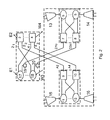
- Fig. 2 shows a schematic drawing of a second embodiment with ingress power splitters instead of ingress WS-switches
- Fig. 3 shows a schematic drawing of a third embodiment with improved cross-connect possibilities
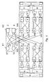
- Fig. 4 shows a schematic drawing of a fourth embodiment with ingress power splitters instead of ingress WS-switches with improved cross-connect possibilities
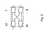
- Fig. 5 shows a schematic drawing of a further embodiment of an add or drop arrangement
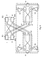
- Fig. 6 shows a schematic drawing of a simplified third embodiment with less switching capabilities of the drop and add arrangements.
- Fig. 1 shows a schematic drawing of a first embodiment of the invention. Elements for amplifying or attenuating signals are not shown for clarity reasons and also not mentioned in the description.
- the basic cross-connect shown in this figure has a plurality of ingress wavelength selective switches and egress wavelength selective switches, which are further down referred to as WSS or WS-switches. Only two ingress WS-switches 1 and 3 and only two egress WS-switches 2 and 4 are shown.
- the first WS-switch 1 receives at an ingress port 1 1 a first DWDM signal E1 (dense wavelength division signal; dense is here not restricted to a certain channel spacing) from a first direction, e.g.
- E1 dense wavelength division signal
- the first egress WSS 2 transmits a second DWDM signal E2 in this direction at an egress port 2 3 .
- Both ports represent a bidirectional port for exchanging DWDM signals in the first direction "east”.
- the other couples of ingress and egress WS-switches e.g. ingress WSS 3 and egress WSS 4, exchange DWDM signals W3, W4 via an ingress port 3 1 and an egress port 3 3 in a second direction "west”.
- An ingress WS-switch 1, 3 has a plurality of outputs.
- the through or express channels of the received DWDM signals are output at "through outputs".
- Each through output 1 2 and 3 2 is connected to a "through input" 2 1 or 4 1 respectively of an egress WSS 2 or 4, which transmits a DWDM signal W4, E2 in another direction as in the direction from which the DWDM signal is received.
- a through channel (or more exact through/express signal) received at the ingress WSS 1 from the direction east is e.g. transferred to the egress node 4 and send in the direction west.
- Cross-connects are usually designed for more than two directions, but only the connections for two directions are shown for clarity reasons.
- Each ingress WSS 1 or WSS3 has beside the through outputs at least one additional output 1 3 , 3 3 , which is called a "drop output” used to output a WDM drop signal.
- a "drop output” used to output a WDM drop signal.
- odd channels channel 1, 3, 5, ...) are dropped at a WSS drop output, this is every second channel of the DWDM signal or, in other words:
- These are the channels of the standard grid for WDM signals with a frequency spacing of 100 GHz or only the "offset" channels (channel 2, 4, 6, ...) shifted by 50 GHz.
- this cross-connect is designed for dropping and adding only odd channels the next cross-connect in a transmission line can be designed for dropping the even channels (of course, also e.g. every fourth or sixth channel can also be output).
- All drop outputs 1 3 , 3 3 of the ingress WS-switches 1 and 3 are connected with drop inputs of a drop arrangement 5,6,7,8.
- a common drop arrangement for a two directions cross-connect comprises two drop power splitters 5 and 6, each receiving a WDM drop signal D1 or D3 respectively, and two drop WS-switches 7 and 8. Outputs of the power splitters 5 and 6 are connected with an input of each drop WS-switch 7 or 8 respectively. Therefore each drop WSS 7 or drop WSS 8 receives a combination of a first and a second WDM drop signal D1 and D3.
- the drop arrangement has a possibility to select certain channels and to feed the selected channels, referred to as "WDM client drop signals", to a certain demultiplexer 13 or 14, which outputs singularized client drop signals CD13, CD14.
- a basic cross-connect as shown in Fig. 1 can be upgraded easily if power splitters with a plurality outputs and WS-switches with a plurality of inputs are used. Each drop signal passes only once a narrow filter of an ingress WSS.
- a common add arrangement 9,10,11,12 is designed similar to the drop arrangement and comprises WS-switches 9, 10 and power splitters 11, 12 used as power combiners.
- Two add WS-switches 9 and 10 receive multiplexed client add signals CA15, CA16 of the same frequency grid, referred to as "WDM client add signals", from multiplexers 15 and 16 respectively.
- Outputs of each WSS 9, 10 are connected with an input off all power combiners 11, 12, an add output of the combiner 11 is connected to an add input 2 2 of the first egress WSS 3 and an add output of the combiner 12 is connected to an add input 4 2 of the second egress WSS 4.
- the received client add signals CA15, CA16 meet also the requirements of the WDM standard grid and therefore correspond to the odd channels. These channels are combined by multiplexers 15 and 16, pre-selected by the add WS-switches 9, 10 - both have the frequency spacing of the standard grid (100 GHz) and the broad pass-band of the standard grid channels, which is about the double bandwidth of the DWDM channels - and fed to the power combiners 11 and 12 to be combined to WDM add signals A2, A4, which are fed to the add inputs 2 2 and 4 2 of the egress WS-switches.
- the add arrangement has also a switching flexibility and can feed the clients signals to a selected egress WSS.
- the WDM add signals A2, A4 are inserted into the transmitted DWDM signals E2, W4 by the egress WS-switches 2 and 4.
- Each client add signal CA15, CA16 passes only once a narrow filter of an egress WSS.
- all through channels are selected by the ingress WS-switches 1 and 3 and fed to another egress WSS 4 or 2
- another egress WSS 4 or 2 (“another" egress WSS, e.g. 2, is defined as an WSS, which transmits a DWDM signal, e.g. W4, in another user-defined direction, e.g. west", and not in the direction, e.g. "east", from which the selected channel is received by the ingress WSS, e.g. WSS1, as part of the DWDM signal E1.
- all WDM drop signals D1, D3 are also selected by the ingress WS-switches 1 and 3 and fed to the drop arrangement.
- the received client add channels are combined to WDM add signals in the add arrangement and fed to the egress WS-switches.
- the cross-connect is designed for more than two directions more WS-switches with additional outputs and inputs are necessary and the drop and add arrangements are also upgraded. If, in addition, the cross-connect is designed for more traffic directions and therefore comprising additional ingress WS-switches and additional egress WS-switches (but still only odd or even) WDM signals, then it is necessary to upgrade the drop and the add arrangement. Additional power splitters with a further outputs and an additional WS-switches with further inputs must be inserted in the drop arrangement and additional demultiplexers and power combiners in the add arrangement. For every additional ingress WSS (or for each further direction) an additional power splitter and an additional WSS and also an additional demultiplexer is necessary. The add arrangement is upgraded in an appropriate way. Of course there are also some less complex solutions but less flexibly solutions possible.
- Fig. 1 shows a drop arrangement comprising a first monitoring device 41 and a second monitoring device 42.
- the quality of the WDM drop signals is monitored. Protection switching of important channels is initiated if a received DWDM signal, e.g. E1, has a very bad quality or if the transmission line of WSS 1 is interrupted. Protection switching is of course also possible in the other embodiments of the invention.
- Fig. 2 shows a second embodiment of the invention.
- the ingress WS-switches 1, 3 are substituted by ingress power splitters 17 and 18.
- An interleaver 19, respectively 20 is inserted downstream of the drop output of each power splitter (the received DWDM signal E1, respectively W2 is output at all through and outputs of the power splitters) to output an odd WDM drop signal D1o, D3o comprising only odd drop channels (or only even drop channels), which are fed to the drop inputs of the drop arrangement 7,8,5,6.
- the power splitters 5, 6 and the WS-switches 7, 8 have interchanged their positions (also the arrangement described before can be used).
- the drop channels are now elected by the WS-switches 7, 8 and the selected drop channels are combined by the power splitters 5, 6, and fed to the demultiplexers 13 and at least 14.
- the positions of the power splitters 11, 12 and the WS-switches 9, 10 are interchanged (but the arrangement described before can also be used).
- the combined client signals are fed to both add WS-switches 9, 10, which output the first WDM add signal A2 and the second WDM add signal A4 respectively. These signals are fed to the add inputs 2 2 and 4 2 of the egress WS-switches 2 and 4 respectively.
- Fig. 3 shows a third embodiment with full drop and full add capability. At least two outputs of each ingress WSS1 and at least WSS3 are used as drop outputs, the first "odd drop output” 1 3 , 3 3 outputs a first "odd WDM drop signal" D1 representing only odd channels according to the 100 GHz ITU standard grid and a second drop output, the "even drop output” 1 4 , 3 4 drops a shifted first "even WDM drop signal" D2 representing only even channels according to a 50 GHz shifted "offset grid". The ingress WSS2 outputs a second "odd WDM drop signal" D3 and a second "even WDM drop signal” D4.
- All odd WDM drop signals D1, D3 with odd channels are fed to the first drop arrangement 5,6,7,8, and all shifted even WDM drop signals D2, D4 with even channels are fed to a second drop arrangement 21,22,23,24. Odd and even channels are separately combined with odd and respectively even channels received from other directions (not shown) as described before. Additional demultiplexers 29 and 30 are used to singularize the even drop channels.
- An appropriate second add arrangement 25,26,27,28 and additional multiplexers 34, 35 are used to combine the even client add signals and to select two shifted WDM add signals A3 and A5. These signals are fed to the two second add inputs 2 4 , 4 4 off the egress WS-switches 2, 4 and inserted into the transmitted DWDM signals E2, W4.
- the third embodiment shows in addition optical switch matrices (arrays) 31, 32, which are connected to output terminals of the demultiplexers 13, 14, 29, 30.
- An additional M(NxK) switch matrices 33 are inserted downstream the switch matrices 31, 32.
- MxN is the number of drop channels.
- each drop channel could be output at each output terminal of the NxN switch matrix.
- the same switch arrangement with a M(NxN) switch matrix 38 and switching matrices 36, 37 can be used at the add site.
- Each add channel can be inserted in each of the WDM add signals.
- switch matrices 33 with more outputs could be used and at the add side switch matrices 38 with more inputs could be used.
- the switching matrices can be substituted by electrical switch matrices and transponders if optical-electrical and electrical-optical conversion is used.
- Fig. 4 shows a fourth embodiment, where, according to Fig. 2 , the ingress WS-switches 1, 3 are replaced by optical splitters 17, 18, but in addition to the embodiment shown in Fig. 2 both outputs of the deinterleavers 19, 20 are used to drop the odd channels outputted at a first interleaver output as well as the even channels outputted at a second interleaver output.
- the odd WDM drop signals D1o and D3o comprising only odd channels are fed to the power splitters 5 and 6 respectively, split and fed to the inputs of the WS-switches 7 and 8. All even WDM drop signals comprising only even channels are fed via the power splitters 21 and 22 to the inputs of the WS-switches 23 and 24.
- the selection of odd and even channels is executed in the drop arrangements by the drop WS-switches 7, 8 and 23, 24.
- a drop arrangement according to Fig. 3 with the same functionality could be also applied in this embodiment.
- Fig. 5 illustrates a further embodiment of a drop arrangement.
- the power splitters 17 and 18 are replaced by WS-switches 51 and 61. Because always two WS-switches with filter characteristics are connected in series, the influence of neighbour channels is reduced.
- Fig. 6 illustrates an embodiment of the cross-connect as shown in Fig. 3 with simplified drop and add arrangements.
- the drop arrangement comprises only power splitters 5, 6 (or WS-switches instead of these power splitters/combiners, not shown). All odd drop channels are combined by the power combiner 5 and all even drop channels are combined the power combiner 6 respectively, which are directly connected to the odd and even drop outputs of the ingress WS-switches 1 and 3.
- the ingress WS-switches 1 and at least 3 are responsible for the selection of all drop channels.
- the selection of the through channels is also carried out by the ingress WS-switches.
- the outputs of the power splitters 5, 6 are connected to e.g. tuneable demultiplexers 13 and 14 respectively.
- the drop arrangement can be upgraded by applying combiners with more inputs.
- the add arrangement is designed in the same way and comprises at least only two power splitters 11, 12. Each power splitter receives only odd or only even client add signals from the (tuneable) multiplexers 15 and 16 and distributes the odd WDM add signals A2, A4 and the even WDM add signals A3, A5 to the odd or even add inputs off the egress WS-switches, which are responsible for the selection of all add channels.
- the add arrangement could also be upgraded by applying splitters with more outputs.
- a drop switch matrix 39 connected to the outputs of the demultiplexers 13, 14 and an add switch matrix 40 connected upstream the inputs of the multiplexers 15, 16 enable a satisfactory switching flexibility for many applications.
Landscapes
- Engineering & Computer Science (AREA)
- Computer Networks & Wireless Communication (AREA)
- Signal Processing (AREA)
- Optical Communication System (AREA)
- Polymers With Sulfur, Phosphorus Or Metals In The Main Chain (AREA)
- Organic Low-Molecular-Weight Compounds And Preparation Thereof (AREA)
- Macromolecular Compounds Obtained By Forming Nitrogen-Containing Linkages In General (AREA)
Abstract
If in another embodiment both odd and even channels are dropped and added, separate add and drop paths are provided for the odd and for the even channels.
Description
- The invention is directed to a photonic cross-connect with add-drop functions. Photonic (also called optical) cross-connects are based on the idea that a channel (more exactly a single signal) from a plurality of received WDM signals (wavelength division multiplex signals) can be redirected into any one of transmitted WDM signals. Most of the cross-connects avoid wavelength conversion, because it is cost effective and, if optical-electrical conversion and 3R-regeneration is not used, reduces the signal quality. Another restriction for the signal quality comes from the wavelength selective elements. These problems increase, if DWDM signals (dense wavelength division multiplex signals) are transmitted.
- To singularize single channels (single signals) of a DWDM signal and to combine a plurality of channels to a DWDM signal, it is necessary to use very narrow filters or similar wavelength selecting elements. This results in a reduction of signal quality. For dropping and adding channels (single signals) from and respectively to a DWDM signal, wavelength selecting elements are also necessary, but neither the quality of the dropped channels nor the quality of the added channels should be reduced. Beside this, a certain switching flexibility is also necessary for outputting drop signals and for inserting add signals.
- Modern photonic cross-connects comprise optical multiplexers, demultiplexers, tuneable filters and wavelength selective switches. A photonic cross-connect is disclosed in the patent application
US 2006/0098981 A1 . Each through or express channel has to pass through a WSS (wavelength selective switch) and a multiplexer. This can be accepted in most cases. But each add and each drop signal has to pass through three narrow filter elements, this means that each signal (referred to as channels) has to pass three narrow filter elements in an add path and at least three narrow filter elements in an drop path even in a short point to point connection. The result is a significant reduction of signal quality. - WS-switches are used for realizing cross-connect and add-drop functions. A WSS functionality can be realized by different technologies. By means of these technologies, e.g. micro-electro-mechanical-systems (MEMS), an optical WDM signal received by an input port can be switched frequency selective to a plurality of output ports and vice versa. The realisation of a frequency-selective switching matrix with a plurality of inputs and outputs is possible by applying these elements.
- It is an object of the invention to overcome the described problems and to find a cross-connect offering high signal quality cross-connections and sufficient add-drop flexibility.
- A way to overcome the signal quality problem is achieved by a photonic cross-connect according to
claim 1. - The improvement in signal quality is obtained by separate processing of odd and even drop channels and odd and even add channel. The drop and the add signals have to pass only wide filters in the whole drop path, e.g. a deinterleaver, a drop arrangement and a demultiplexer, respectively in the add path, e.g. a multiplexer and an add arrangement.
- The impairment of signal quality of the through/express signals is reduced by substituting the ingress WS-switches by power splitters according to
claim 2. - Full add and drop capability is achieved if odd and even channels are dropped according to
claim 3. The odd and even channels are also processed separately. - According to
claim 4 the advantages according toclaim - If only a few add and drop channels are needed, simple but upgradeable add and drop arrangements according to
claim 5 reduce the costs for a basic network. - According to
claim 6 the switching flexibility on the client side is improved if add and drop arrangements with switching capability are used. The drop and the add arrangement can be upgraded to cross-connect-arrangements. - According to
claim 7 the power splitters are substituted by additional WS-switches to improve crosstalk properties. - According to
claim 8 cost-effective drop and add arrangements can be even used, if only a few odd and even channels are dropped and inserted. - According to
claim 9 it is advantageously to use at least one demultiplexer with the standard grid or the offset grid to singularize only odd or only even drop channels and at least one multiplexer with the standard grid or the offset grid to combine only odd channels or only even channels. - According to
claim 10 it is advantageously to use at least two different demultiplexers, whose inputs are connected to outputs of the drop arrangements and at least two different multiplexers, whose outputs are connected to inputs of the add arrangement. A plurality of switching possibilities of the drop and add arrangement and of the demultiplexers and multiplexers enables the dropping and adding of channels (signals) carrying signals of the same frequency. At least two different demultiplexers and multiplexers are always necessary because odd and even channels have to be processed separately. - According to
claim 11, which refers to drop and add arrangements for odd and even channels, it is advantageously to use at least two demultiplexers, whose inputs are connected to outputs of the first drop arrangements and at least two further demultiplexers, whose inputs are connected to outputs of the second drop arrangements and at least two multiplexers and two further multiplexers, whose outputs are connected to inputs of the at least two add arrangement. Odd and even channels are processed in different demultiplexers and multiplexers with standard and offset grid separately to avoid an impairment of signal quality. - The switching capability for client drop signals and client add can be improved by using optical or electrical switch matrices according to the claims 12 - 14.
- It is advantageously to integrate signal quality monitors according to claim 15 to initiate protection switching.
- Examples of the invention of preferred embodiments are described below with reference to accompanying figures, where
Fig. 1 shows a schematic drawing of a first embodiment of a photonic cross-connect comprising ingress and egress wavelength selective switches,Fig. 2 shows a schematic drawing of a second embodiment with ingress power splitters instead of ingress WS-switches,Fig. 3 shows a schematic drawing of a third embodiment with improved cross-connect possibilities,Fig. 4 shows a schematic drawing of a fourth embodiment with ingress power splitters instead of ingress WS-switches with improved cross-connect possibilities,Fig. 5 shows a schematic drawing of a further embodiment of an add or drop arrangement, andFig. 6 shows a schematic drawing of a simplified third embodiment with less switching capabilities of the drop and add arrangements. -
Fig. 1 shows a schematic drawing of a first embodiment of the invention. Elements for amplifying or attenuating signals are not shown for clarity reasons and also not mentioned in the description. The basic cross-connect shown in this figure has a plurality of ingress wavelength selective switches and egress wavelength selective switches, which are further down referred to as WSS or WS-switches. Only two ingress WS-switches switches switch 1 receives at an ingress port 11 a first DWDM signal E1 (dense wavelength division signal; dense is here not restricted to a certain channel spacing) from a first direction, e.g. "east", and the first egress WSS 2 transmits a second DWDM signal E2 in this direction at anegress port 23. Both ports represent a bidirectional port for exchanging DWDM signals in the first direction "east". The other couples of ingress and egress WS-switches, e.g. ingress WSS 3 and egress WSS 4, exchange DWDM signals W3, W4 via aningress port 31 and anegress port 33 in a second direction "west". - An ingress WS-
switch output egress WSS ingress WSS 1 from the direction east is e.g. transferred to theegress node 4 and send in the direction west. Cross-connects are usually designed for more than two directions, but only the connections for two directions are shown for clarity reasons. - Each
ingress WSS 1 or WSS3 has beside the through outputs at least oneadditional output
According to this embidiment only e.g. odd channels (channel channel - All
drop outputs switches drop arrangement - Because only two ingress WS-switches are shown in
Fig. 1 for clarity reasons, only few elements of the drop arrangement are illustrated. A common drop arrangement for a two directions cross-connect comprises twodrop power splitters switches power splitters switch drop WSS 7 or drop WSS 8 receives a combination of a first and a second WDM drop signal D1 and D3. The drop arrangement has a possibility to select certain channels and to feed the selected channels, referred to as "WDM client drop signals", to acertain demultiplexer - If the switching flexibility of this "drop matrix" is not needed, or if a system is installed for only a few clients, all the WDM drop signals of the same WDM grid can be combined and output by only one
demultiplexer 13. A basic cross-connect as shown inFig. 1 can be upgraded easily if power splitters with a plurality outputs and WS-switches with a plurality of inputs are used. Each drop signal passes only once a narrow filter of an ingress WSS. - A
common add arrangement switches power splitters switches multiplexers WSS power combiners combiner 11 is connected to an addinput 22 of thefirst egress WSS 3 and an add output of thecombiner 12 is connected to an addinput 42 of thesecond egress WSS 4. - The received client add signals CA15, CA16 meet also the requirements of the WDM standard grid and therefore correspond to the odd channels. These channels are combined by
multiplexers switches 9, 10 - both have the frequency spacing of the standard grid (100 GHz) and the broad pass-band of the standard grid channels, which is about the double bandwidth of the DWDM channels - and fed to thepower combiners add inputs - The add arrangement has also a switching flexibility and can feed the clients signals to a selected egress WSS. The WDM add signals A2, A4 are inserted into the transmitted DWDM signals E2, W4 by the egress WS-
switches - To summarise, according to this arrangement all through channels are selected by the ingress WS-
switches egress WSS 4 or 2 ("another" egress WSS, e.g. 2, is defined as an WSS, which transmits a DWDM signal, e.g. W4, in another user-defined direction, e.g. west", and not in the direction, e.g. "east", from which the selected channel is received by the ingress WSS, e.g. WSS1, as part of the DWDM signal E1. As mentioned before, all WDM drop signals D1, D3 are also selected by the ingress WS-switches - If the cross-connect is designed for more than two directions more WS-switches with additional outputs and inputs are necessary and the drop and add arrangements are also upgraded. If, in addition, the cross-connect is designed for more traffic directions and therefore comprising additional ingress WS-switches and additional egress WS-switches (but still only odd or even) WDM signals, then it is necessary to upgrade the drop and the add arrangement. Additional power splitters with a further outputs and an additional WS-switches with further inputs must be inserted in the drop arrangement and additional demultiplexers and power combiners in the add arrangement. For every additional ingress WSS (or for each further direction) an additional power splitter and an additional WSS and also an additional demultiplexer is necessary. The add arrangement is upgraded in an appropriate way. Of course there are also some less complex solutions but less flexibly solutions possible.
- The embodiment of
Fig. 1 shows a drop arrangement comprising afirst monitoring device 41 and asecond monitoring device 42. The quality of the WDM drop signals is monitored. Protection switching of important channels is initiated if a received DWDM signal, e.g. E1, has a very bad quality or if the transmission line ofWSS 1 is interrupted. Protection switching is of course also possible in the other embodiments of the invention. -
Fig. 2 shows a second embodiment of the invention. The ingress WS-switches ingress power splitters interleaver 19, respectively 20 is inserted downstream of the drop output of each power splitter (the received DWDM signal E1, respectively W2 is output at all through and outputs of the power splitters) to output an odd WDM drop signal D1o, D3o comprising only odd drop channels (or only even drop channels), which are fed to the drop inputs of thedrop arrangement power splitters switches switches power splitters demultiplexers 13 and at least 14. - Also in the add arrangement are the positions of the
power splitters switches switches add inputs switches - The advantage of this arrangement is obvious: Also the through channels have to pass only a narrow bandwidth filter element in the egress WSS only once, but the switching flexibility of the ingress WS-switches is missing.
-
Fig. 3 shows a third embodiment with full drop and full add capability. At least two outputs of each ingress WSS1 and at least WSS3 are used as drop outputs, the first "odd drop output" 13, 33 outputs a first "odd WDM drop signal" D1 representing only odd channels according to the 100 GHz ITU standard grid and a second drop output, the "even drop output" 14, 34 drops a shifted first "even WDM drop signal" D2 representing only even channels according to a 50 GHz shifted "offset grid". The ingress WSS2 outputs a second "odd WDM drop signal" D3 and a second "even WDM drop signal" D4. - All odd WDM drop signals D1, D3 with odd channels are fed to the
first drop arrangement second drop arrangement Additional demultiplexers - According to the ingress WS-
switches switches input second add arrangement additional multiplexers second add inputs switches - Because all odd and all even channels are processed separately in the add and in the drop arrangements, all add signals and all drop signals have to pass a narrow filter element only once in an ingress WSS or in an egress WSS respectively.
- The third embodiment shows in addition optical switch matrices (arrays) 31, 32, which are connected to output terminals of the
demultiplexers switch matrices 33 are inserted downstream theswitch matrices switch matrices switch matrix 38 and switchingmatrices matrices 33 with more outputs (K > N) could be used and at the addside switch matrices 38 with more inputs could be used. The switching matrices can be substituted by electrical switch matrices and transponders if optical-electrical and electrical-optical conversion is used. -
Fig. 4 shows a fourth embodiment, where, according toFig. 2 , the ingress WS-switches optical splitters Fig. 2 both outputs of thedeinterleavers power splitters switches power splitters switches switches Fig. 3 with the same functionality could be also applied in this embodiment. -
Fig. 5 illustrates a further embodiment of a drop arrangement. Thepower splitters switches -
Fig. 6 illustrates an embodiment of the cross-connect as shown inFig. 3 with simplified drop and add arrangements. - The drop arrangement comprises only
power splitters 5, 6 (or WS-switches instead of these power splitters/combiners, not shown). All odd drop channels are combined by thepower combiner 5 and all even drop channels are combined thepower combiner 6 respectively, which are directly connected to the odd and even drop outputs of the ingress WS-switches switches 1 and at least 3 are responsible for the selection of all drop channels. The selection of the through channels is also carried out by the ingress WS-switches. The outputs of thepower splitters tuneable demultiplexers - The add arrangement is designed in the same way and comprises at least only two
power splitters multiplexers - A
drop switch matrix 39 connected to the outputs of thedemultiplexers add switch matrix 40 connected upstream the inputs of themultiplexers -
- 1
- first ingress WSS (wavelength selective switch)
- 2
- first egress WSS
- 3
- second ingress WSS
- 4
- second first egress WSS
- 5
- first drop power splitter
- 6
- second drop power splitter
- 7
- first add WSS
- 8
- second add WSS
- 9
- first add WSS
- 10
- second add WSS
- 11
- first add power splitter/combiner
- 12
- second add power splitter/combiner
- 13
- first demultiplexer
- 14
- second demultiplexer
- 15
- first demultiplexer
- 16
- second demultiplexer
- 17
- first ingress power splitter
- 18
- second ingress power splitter
- 19
- first deinterleaver
- 20
- second deinterleaver
- 21
- drop power splitter
- 22
- drop power splitter
- 23
- drop WSS
- 24
- drop WSS
- 25
- add WSS
- 26
- add WSS
- 27
- add power splitter/combiner
- 28
- add power splitter/combiner
- 29
- demultiplexer
- 30
- demultiplexer
- 31
- switch matrix
- 32
- switch matrix
- 33
- NxN switch matrix
- 34
- multiplexer
- 35
- multiplexer
- 36
- switch matrix
- 37
- switch matrix
- 38
- NxN switch matrix
- 39
- add switch matrix
- 40
- drop switch matrix
- 41
- first monitoring device
- 42
- second monitoring device
- 11
- first ingress port of WSS1
- 23
- first egress port
- 31
- first ingress port
- 43
- second egress port
- 14
- second drop output of WSS1
- 34
- second drop output
- E1
- received DWDM signal "east"
- E2
- transmitted DWDM signal "east"
- W3
- received DWDM signal "west"
- W4
- transmitted DWDM signal "west"
- D1
- first WDM drop signal
- D2
- first WDM drop signal
- D1o
- first odd WDM drop signal
- D1e
- first even WDM drop signal
- D3
- second (odd) WDM drop signal
- D4
- second even WDM drop signal
- A2
- first (odd) WDM add signal
- A3
- first even WDM add signal
- A4
- second (odd) WDM add signal
- A5
- second even WDM add signal
Claims (15)
- A photonic cross-connect comprising a first ingress port (11) receiving a first DWDM (dense wavelength division multiplex) signal (E1) connected to an input of a first ingress (wavelength selective switch) WSS (1), an egress port (23) connected to an output of a first egress WSS (2) transmitting a second DWDM signal (W2), the first ingress port (11) and the first egress port (23) representing a bidirectional port for exchanging DWDM signals (E1, E2) in a first direction, at least a second ingress port (31) receiving a third DWDM signal (W3) connected to an input of at least a second ingress WSS (3) and at least a second egress port (43) connected to an output of at least a second egress WSS (4) transmitting a fourth DWDM signal (W4), the second ingress port (31) and the second egress port (43) representing a bidirectional port for exchanging DWDM signals (W3, W4) in a second direction, the first and the at least second ingress WSS (1, 3) having at least one through output (12, 32), each through output (12, 32) being connected to an through input (41, 21) of each other egress WSS (4, 2) transmitting DWDM signals (W4, E2) in another direction, the first and the at least second ingress WSS (1, 3) having drop outputs (13, 33) outputting a first WDM drop signal (D1) and respectively at least a second WDM drop signal (D2), both WDM drop signals (D1, D2) comprising only odd or only even channels, the first and the at least second egress WSS (2, 4) having add inputs (22, 42) for receiving a first WDM add signal (A2) and at least a second WDM add signal (A4) respectively, both WDM add signals (A2, A4) comprising only odd or only even channels, a drop arrangement (5-8) with a first and at least a second drop input (D1, D3), connected to drop outputs (13, 33) of the first and at least the second ingress WSS (1, 3) respectively, the drop arrangement (5-8) combining only odd channels or only even channels of said WDM drop signals (D1, D2), and with at least one output connected to a drop demultiplexer (13) singularizing said WDM drop signals (D1, D2) into client drop signals (CD13), an add arrangement (9-12) with at least one input connected to an output of a multiplexer (15) combining received client add signals (CA15) , with a first add output and at least a second add output connected to the add inputs (22, 42) of the first egress WSS (2) and the at least second egress WSS (4) respectively, and wherein all wavelength selective elements (7, 8, 13, 14) in a drop path (5-8) and in an add path (9-11) comply with at least a double frequency spacing and about a double bandwidth of the ingress WS-switches (1, 2) or egress WS-switches (2, 4).
- A photonic cross-connect according to claim 1,
characterized in that the ingress WS-switches (1, 3) are substituted by power splitters (17, 18), through outputs of the power splitters (17, 18) are fed to an through input (21, 41) of each other egress WS-switches (4, 3), and a deinterleaver (19, 20) is inserted downstream of a drop output of each power splitter (17, 18), and that only the odd or only the even channels are outputted from outputs of the deinterleavers (19, 20) and fed to the drop arrangement (5-8). - A photonic cross-connect according to claim 1 or 2,
characterized in that the ingress WS-switches (1, 3) have beside a first drop outputs (13, 33) for outputting odd WDM drop signals (D1, D3) comprising only odd drop channels a second drop output (14, 34) for outputting even WDM drop signals (D2, D4) comprising only even drop channels, the egress WS-switches (2, 4) have beside a first add input (22, 42) for receiving odd WDM add signals (A2, A4) with only odd channels a second add input (24, 44) for receiving an even WDM add signal (A3, A5) with only even channels, and that the odd WDM drop signals (D1, D3) are fed to the first drop arrangement (5-8) and the even WDM drop signals (D2, D4) are fed to the second drop arrangement (21-24) and the odd WDM add signals (A2, A4) are output from the first add arrangement (9-12) and the even WDM add signals (A3, A5) are output from a second add arrangement (25-28). - A photonic cross-connect according to claim 3, characterized in that the ingress WS-switches (1, 3) are substituted by power splitters (17, 18), the through outputs (13, 33) of the power splitters (17, 18) are fed to an input of the other egress WS-switches (4, 2) for transmitting a DWDM signal (W4, W2) in another direction, and that a deinterleaver (19, 20) is inserted downstream of a drop output of each power splitter (17, 18) outputting an odd WDM drop signal (D1o, D3o) with only odd channels and the even WDM drop signal (D2e, D4e) with only even channels.
- A photonic cross-connect according to one of the preceding claims,
characterized in that the drop arrangement (5-7) comprises at least two power splitters (5, 6) receiving WDM drop signals (D1, D3) and one WSS (7) or vice versa and the add arrangement (9-11) comprises at least one add WSS (9) and two power splitters (11, 12) or vice versa outputting WDM add signals (A2, A4), wherein the drop WS-switches (7, 8) and add WS-switches (9, 10) comply with a double frequency spacing and about a double bandwidth of the ingress WS-switches (1, 3) or egress WS-switches (2, 4) respectively. - A photonic cross-connect according to one of the preceding claims 1 - 4,
characterized in that the drop arrangement (5-8, 21-24) comprises a first power splitter (5) and at least a second power splitter (6) receiving WDM drop signals (D1, D3) with at least two outputs each, and a first drop WSS (7) and least a second drop WSS (8) with at least two inputs each, wherein a first output of each drop power splitter (5,6) is fed to a first and at least a second input of the first drop WSS (7), and a second output of each drop power splitter (5,6) is fed to a first and at least a second input the at least second WSS (8) or vice versa, the add arrangement (9-12; 25-28) comprises a first add WSS (9) and at least a second add WSS (10) with at least two outputs each, and a first power splitter (11) and at least a second power splitter (12) with at least two inputs each and outputting WDM add signals (A2, A4), wherein first outputs of the first and the at least second add WSS (9, 10) are fed to a first and at least a second input of the first power splitter (11); and second outputs of the first and the at least second add WSS (9,10) are fed to a first and at least a second input of the at least second power splitter (12) or vice versa, wherein all drop WS-switches (7, 8) and all add WS-switches (9, 10) comply with at least a double frequency spacing and about a double bandwidth of the ingress WS-switches (1, 3) or egress WS-switches (2, 4) respectively. - A photonic cross-connect according to claim 6, characterized in that the power splitters (5, 6) or power combiners (11, 12) are substituted by additional wavelength selective switches ( 51, 61) .
- A photonic cross-connect according to claim 3, characterized in that the drop arrangement (5,6) comprises a first power combiner (5) for combining odd WDM drop signals (D1, D3) and a second power combiner (6) for combining even WDM drop signals (D2, D4), the add arrangement (11,12) comprises a first power splitter (11) for outputting odd WDM add signals (A2, A4) with only odd channels and a second power splitter (12) for outputting even WDM Add signals (A3, A5) with only even channels.
- A photonic cross-connect according to one of the preceding claims,
characterized in that at least one demultiplexer (13, 14) is inserted downstream of the drop arrangement (5-8) for singularizing a WDM client drop signal into a client drop signals (CD13) and at least one multiplexer (15, 16) inserted upstream of the add arrangement for receiving client add signals and combining these signals (CA15) to a WDM client add signal. - A photonic cross-connect according to one of the claims 6 - 8,
characterized in that at least two demultiplexers (13, 14) are inserted downstream of the drop arrangement (5-8) for singularizing first WDM client drop signals with only odd channels into client drop signals (CD13, CD14) and at least two multiplexers (15, 16) are inserted upstream of the add arrangement (9-12) for receiving client add signals (CA15, CA16) with only odd channels and combining these signals to first WDM client add signals (A2, A4). - A photonic cross-connect according to claim 3 or 4,
characterized in that at least two demultiplexers (13, 14) inserted downstream of the first drop arrangement (5-8) for singularizing first WDM client drop signals with only odd channels and at least two further demultiplexers (29,30) inserted downstream of the second drop arrangement (21-24) for singularizing second WDM client drop signals with only even channels into further client drop signals (CD29, CD30), at least two multiplexers (15, 16) inserted upstream of the first add arrangement (9-12) for receiving client add signals (CA15, CA16) with only odd channels and combining these signals to first WDM client add signals and at least two multiplexers (34, 35) inserted upstream of the second add arrangement (25-28) for receiving client add signals (CA25, CA26) with only even channels and combining these signals to second WDM client add signals (A3, A5) with only even channels. - A photonic cross-connect according to one of the claims 9 or 10,
characterized in that a drop switch matrix (39; 31, 32) connected downstream of outputs of the demultiplexers (13, 14, 29, 30) of the drop arrangement (5-8) and outputting client drop signals (CD13, CD14), an add switch matrix (40; 36, 37) connected upstream to inputs of the multiplexers (15, 16, 34, 35) of the add arrangement (9-12; 25-28) and receiving client add signals (CA15, CA16) at its inputs. - A photonic cross-connect according to claim 12,
characterized in that a first drop switch matrix (31) is connected downstream of each first demultiplexer (13, 29) of the first and of at least a second drop arrangement (5-8; 21-24) and a second drop switch matrix (32) is connected downstream of each second demultiplexer (14, 30) of the first and of the at least second drop arrangement (5-8; 21-24), a first add switch matrix (36) is connected upstream of each first add multiplexer (13, 34) of the first and at least a second add arrangement (9-12; 25-28) and a second add switch matrix (37) is connected upstream of each second add multiplexer (16, 35) of the first and the at least second add arrangement (9-12; 25-28). - A photonic cross-connect according to claim 12 or 13,
characterized in that a M(NxK) drop switch matrix (33), wherein N and K are at least equal to the number of the drop switch matrices (31, 32), MxK is the number of outputs and MxN the number of inputs, is connected downstream of the drop switching matrices (31, 32) and a M(NxK) add switching matrix (38) , wherein N and K are at least equal to the number of the add switching matrices (36, 37) and MxK is the number of outputs and MxN the number of inputs, is connected upstream the add switching matrices (36, 37). - A photonic cross-connect according to one of the preceding claims,
characterized in that the drop arrangement (5,6,7,8) comprises monitoring devices (41, 42) for protection switching.
Priority Applications (6)
| Application Number | Priority Date | Filing Date | Title |
|---|---|---|---|
| AT07022625T ATE504126T1 (en) | 2007-11-21 | 2007-11-21 | PHOTONIC CROSSCONNECT |
| EP07022625A EP2063562B1 (en) | 2007-11-21 | 2007-11-21 | Photonic cross-connect |
| DE602007013576T DE602007013576D1 (en) | 2007-11-21 | 2007-11-21 | Photonic Crossconnect |
| CA2644351A CA2644351C (en) | 2007-11-21 | 2008-11-20 | Photonic cross-connect |
| CN2008101895901A CN101483493B (en) | 2007-11-21 | 2008-11-21 | Photonic cross-connect |
| US12/275,915 US8073332B2 (en) | 2007-11-21 | 2008-11-21 | Photonic cross-connect |
Applications Claiming Priority (1)
| Application Number | Priority Date | Filing Date | Title |
|---|---|---|---|
| EP07022625A EP2063562B1 (en) | 2007-11-21 | 2007-11-21 | Photonic cross-connect |
Publications (2)
| Publication Number | Publication Date |
|---|---|
| EP2063562A1 true EP2063562A1 (en) | 2009-05-27 |
| EP2063562B1 EP2063562B1 (en) | 2011-03-30 |
Family
ID=39232797
Family Applications (1)
| Application Number | Title | Priority Date | Filing Date |
|---|---|---|---|
| EP07022625A Active EP2063562B1 (en) | 2007-11-21 | 2007-11-21 | Photonic cross-connect |
Country Status (6)
| Country | Link |
|---|---|
| US (1) | US8073332B2 (en) |
| EP (1) | EP2063562B1 (en) |
| CN (1) | CN101483493B (en) |
| AT (1) | ATE504126T1 (en) |
| CA (1) | CA2644351C (en) |
| DE (1) | DE602007013576D1 (en) |
Cited By (1)
| Publication number | Priority date | Publication date | Assignee | Title |
|---|---|---|---|---|
| US20220182169A1 (en) * | 2019-03-26 | 2022-06-09 | Nippon Telegraph And Telephone Corporation | Optical branch insertion device and optical transmission system using optical branch insertion device |
Families Citing this family (6)
| Publication number | Priority date | Publication date | Assignee | Title |
|---|---|---|---|---|
| US20110164876A1 (en) * | 2008-10-02 | 2011-07-07 | Enablence USA Components, Inc. | Directionless reconfigurable optical add/drop multiplexer |
| US9331807B2 (en) * | 2012-10-15 | 2016-05-03 | Telefonaktiebolaget L M Ericsson (Publ) | Service edge hub device and methods in an optical network node |
| EP2757714A1 (en) * | 2013-01-18 | 2014-07-23 | Xieon Networks S.à.r.l. | Photonic cross-connect with reconfigurable add-dropfunctionality |
| US9654209B2 (en) * | 2015-04-08 | 2017-05-16 | Nec Corporation | Low cost secure ROADM branching unit with redundancy protection |
| CN107852261B (en) * | 2015-04-24 | 2019-06-25 | 洛克利光子有限公司 | Photoelectric Switch Architecture |
| CN113054991B (en) * | 2021-02-02 | 2022-12-20 | 中国电子科技集团公司第二十九研究所 | Implementation method of switch matrix, switch matrix, module and beamforming network |
Citations (5)
| Publication number | Priority date | Publication date | Assignee | Title |
|---|---|---|---|---|
| US6256433B1 (en) | 1999-09-24 | 2001-07-03 | Wavesplitter Technologies, Inc. | Expandable interleaving optical add/drop filter module |
| US20010024542A1 (en) | 1998-06-09 | 2001-09-27 | Stefano Aina | Method and device for dropping optical channels in an optical transmission system |
| US7043159B1 (en) * | 1999-04-13 | 2006-05-09 | Nortel Networks Limited | Bidirectional optical networks |
| US20060098981A1 (en) | 2004-11-10 | 2006-05-11 | Fujitsu Limited | Optical transmitting apparatus, method of increasing the number of paths of the apparatus, and optical switch module for increasing the number of paths of the apparatus |
| WO2006114435A1 (en) | 2005-04-28 | 2006-11-02 | Nokia Siemens Networks Gmbh & Co. Kg | Arrangements for an add-drop system and transmission system for wavelength multiplex signals |
Family Cites Families (1)
| Publication number | Priority date | Publication date | Assignee | Title |
|---|---|---|---|---|
| JP4638754B2 (en) * | 2005-03-18 | 2011-02-23 | 富士通株式会社 | Optical device and optical cross-connect device |
-
2007
- 2007-11-21 DE DE602007013576T patent/DE602007013576D1/en active Active
- 2007-11-21 AT AT07022625T patent/ATE504126T1/en not_active IP Right Cessation
- 2007-11-21 EP EP07022625A patent/EP2063562B1/en active Active
-
2008
- 2008-11-20 CA CA2644351A patent/CA2644351C/en not_active Expired - Fee Related
- 2008-11-21 CN CN2008101895901A patent/CN101483493B/en active Active
- 2008-11-21 US US12/275,915 patent/US8073332B2/en active Active
Patent Citations (5)
| Publication number | Priority date | Publication date | Assignee | Title |
|---|---|---|---|---|
| US20010024542A1 (en) | 1998-06-09 | 2001-09-27 | Stefano Aina | Method and device for dropping optical channels in an optical transmission system |
| US7043159B1 (en) * | 1999-04-13 | 2006-05-09 | Nortel Networks Limited | Bidirectional optical networks |
| US6256433B1 (en) | 1999-09-24 | 2001-07-03 | Wavesplitter Technologies, Inc. | Expandable interleaving optical add/drop filter module |
| US20060098981A1 (en) | 2004-11-10 | 2006-05-11 | Fujitsu Limited | Optical transmitting apparatus, method of increasing the number of paths of the apparatus, and optical switch module for increasing the number of paths of the apparatus |
| WO2006114435A1 (en) | 2005-04-28 | 2006-11-02 | Nokia Siemens Networks Gmbh & Co. Kg | Arrangements for an add-drop system and transmission system for wavelength multiplex signals |
Cited By (2)
| Publication number | Priority date | Publication date | Assignee | Title |
|---|---|---|---|---|
| US20220182169A1 (en) * | 2019-03-26 | 2022-06-09 | Nippon Telegraph And Telephone Corporation | Optical branch insertion device and optical transmission system using optical branch insertion device |
| US11757554B2 (en) * | 2019-03-26 | 2023-09-12 | Nippon Telegraph And Telephone Corporation | Optical branch insertion device and optical transmission system using optical branch insertion device |
Also Published As
| Publication number | Publication date |
|---|---|
| CN101483493B (en) | 2012-05-30 |
| ATE504126T1 (en) | 2011-04-15 |
| CA2644351C (en) | 2013-03-12 |
| EP2063562B1 (en) | 2011-03-30 |
| CN101483493A (en) | 2009-07-15 |
| US20090142058A1 (en) | 2009-06-04 |
| US8073332B2 (en) | 2011-12-06 |
| CA2644351A1 (en) | 2009-05-21 |
| DE602007013576D1 (en) | 2011-05-12 |
Similar Documents
| Publication | Publication Date | Title |
|---|---|---|
| US8625994B2 (en) | Directionless reconfigurable optical add-drop multiplexer systems and methods | |
| JP5470379B2 (en) | Device for switching optical signals | |
| JP4937983B2 (en) | Optical transmission equipment | |
| US9520959B2 (en) | Optical drop apparatus, optical add apparatus, and optical add/drop apparatus | |
| EP1324523A1 (en) | Wavelength-division multiplexing optical communication system | |
| EP3017558B1 (en) | Photonic switch chip for scalable reconfigurable optical add/drop multiplexer | |
| EP2413527B1 (en) | A directionless and colorless reconfigurable optical add/drop multiplexer | |
| EP2916475B1 (en) | N-degree CDC WSX ROADM | |
| CA2644351C (en) | Photonic cross-connect | |
| JP4843659B2 (en) | Optical transmission network system, optical transmission device, and passband allocation method using them | |
| US8811817B2 (en) | Optical signal transmission device, optical signal reception device, wavelength division multiplexing optical communication device, and wavelength path system | |
| CN101019359B (en) | Reconfigurable WDM add-drop multiplexer and method for operating add-drop nodes | |
| CN104919736B (en) | Photon interconnection with restructural drop and insert feature | |
| EP2979383B1 (en) | Optical switch | |
| JP2014022865A (en) | Optical signal branching device and optical signal insertion device | |
| EP1408713B1 (en) | Optical cross-connect system | |
| JP6130403B2 (en) | Multi-band reconfigurable optical add-drop multiplexing with convergence signal addition and removal | |
| US20060013587A1 (en) | Modular wavelength selective switch | |
| EP1434374A1 (en) | Optical add-drop multiplexer for optical metropolitan networks | |
| EP2403170B1 (en) | A reconfigurable optical add and drop wavelength multiplexer for an optical network using wavelength division multiplexing | |
| EP2928097A1 (en) | Optical switching | |
| US8774631B2 (en) | Switch node | |
| KR100594736B1 (en) | Wavelength selection switch and wavelength selection method | |
| US8611749B2 (en) | Technology for arranging optical channels in switching optical equipment | |
| US20020145784A1 (en) | Optical wavelength switching system with wavelength selective splitters and combiners |
Legal Events
| Date | Code | Title | Description |
|---|---|---|---|
| PUAI | Public reference made under article 153(3) epc to a published international application that has entered the european phase |
Free format text: ORIGINAL CODE: 0009012 |
|
| AK | Designated contracting states |
Kind code of ref document: A1 Designated state(s): AT BE BG CH CY CZ DE DK EE ES FI FR GB GR HU IE IS IT LI LT LU LV MC MT NL PL PT RO SE SI SK TR |
|
| AX | Request for extension of the european patent |
Extension state: AL BA HR MK RS |
|
| 17P | Request for examination filed |
Effective date: 20091127 |
|
| 17Q | First examination report despatched |
Effective date: 20091228 |
|
| AKX | Designation fees paid |
Designated state(s): AT BE BG CH CY CZ DE DK EE ES FI FR GB GR HU IE IS IT LI LT LU LV MC MT NL PL PT RO SE SI SK TR |
|
| RBV | Designated contracting states (corrected) |
Designated state(s): AT BE BG CH CY CZ DE DK EE ES FI FR GB GR HU IE IS IT LI LT LU LV MC MT NL PL PT RO SE SI SK TR |
|
| GRAP | Despatch of communication of intention to grant a patent |
Free format text: ORIGINAL CODE: EPIDOSNIGR1 |
|
| RIC1 | Information provided on ipc code assigned before grant |
Ipc: H04J 14/02 20060101AFI20101008BHEP |
|
| GRAS | Grant fee paid |
Free format text: ORIGINAL CODE: EPIDOSNIGR3 |
|
| GRAA | (expected) grant |
Free format text: ORIGINAL CODE: 0009210 |
|
| AK | Designated contracting states |
Kind code of ref document: B1 Designated state(s): AT BE BG CH CY CZ DE DK EE ES FI FR GB GR HU IE IS IT LI LT LU LV MC MT NL PL PT RO SE SI SK TR |
|
| REG | Reference to a national code |
Ref country code: GB Ref legal event code: FG4D |
|
| REG | Reference to a national code |
Ref country code: CH Ref legal event code: EP |
|
| REG | Reference to a national code |
Ref country code: IE Ref legal event code: FG4D |
|
| REF | Corresponds to: |
Ref document number: 602007013576 Country of ref document: DE Date of ref document: 20110512 Kind code of ref document: P |
|
| REG | Reference to a national code |
Ref country code: DE Ref legal event code: R096 Ref document number: 602007013576 Country of ref document: DE Effective date: 20110512 |
|
| REG | Reference to a national code |
Ref country code: SE Ref legal event code: TRGR |
|
| REG | Reference to a national code |
Ref country code: NL Ref legal event code: VDEP Effective date: 20110330 |
|
| PG25 | Lapsed in a contracting state [announced via postgrant information from national office to epo] |
Ref country code: LV Free format text: LAPSE BECAUSE OF FAILURE TO SUBMIT A TRANSLATION OF THE DESCRIPTION OR TO PAY THE FEE WITHIN THE PRESCRIBED TIME-LIMIT Effective date: 20110330 Ref country code: GR Free format text: LAPSE BECAUSE OF FAILURE TO SUBMIT A TRANSLATION OF THE DESCRIPTION OR TO PAY THE FEE WITHIN THE PRESCRIBED TIME-LIMIT Effective date: 20110701 Ref country code: LT Free format text: LAPSE BECAUSE OF FAILURE TO SUBMIT A TRANSLATION OF THE DESCRIPTION OR TO PAY THE FEE WITHIN THE PRESCRIBED TIME-LIMIT Effective date: 20110330 |
|
| LTIE | Lt: invalidation of european patent or patent extension |
Effective date: 20110330 |
|
| PG25 | Lapsed in a contracting state [announced via postgrant information from national office to epo] |
Ref country code: SI Free format text: LAPSE BECAUSE OF FAILURE TO SUBMIT A TRANSLATION OF THE DESCRIPTION OR TO PAY THE FEE WITHIN THE PRESCRIBED TIME-LIMIT Effective date: 20110330 Ref country code: CY Free format text: LAPSE BECAUSE OF FAILURE TO SUBMIT A TRANSLATION OF THE DESCRIPTION OR TO PAY THE FEE WITHIN THE PRESCRIBED TIME-LIMIT Effective date: 20110330 Ref country code: FI Free format text: LAPSE BECAUSE OF FAILURE TO SUBMIT A TRANSLATION OF THE DESCRIPTION OR TO PAY THE FEE WITHIN THE PRESCRIBED TIME-LIMIT Effective date: 20110330 Ref country code: AT Free format text: LAPSE BECAUSE OF FAILURE TO SUBMIT A TRANSLATION OF THE DESCRIPTION OR TO PAY THE FEE WITHIN THE PRESCRIBED TIME-LIMIT Effective date: 20110330 |
|
| PG25 | Lapsed in a contracting state [announced via postgrant information from national office to epo] |
Ref country code: BE Free format text: LAPSE BECAUSE OF FAILURE TO SUBMIT A TRANSLATION OF THE DESCRIPTION OR TO PAY THE FEE WITHIN THE PRESCRIBED TIME-LIMIT Effective date: 20110330 |
|
| PG25 | Lapsed in a contracting state [announced via postgrant information from national office to epo] |
Ref country code: EE Free format text: LAPSE BECAUSE OF FAILURE TO SUBMIT A TRANSLATION OF THE DESCRIPTION OR TO PAY THE FEE WITHIN THE PRESCRIBED TIME-LIMIT Effective date: 20110330 Ref country code: PT Free format text: LAPSE BECAUSE OF FAILURE TO SUBMIT A TRANSLATION OF THE DESCRIPTION OR TO PAY THE FEE WITHIN THE PRESCRIBED TIME-LIMIT Effective date: 20110801 |
|
| PG25 | Lapsed in a contracting state [announced via postgrant information from national office to epo] |
Ref country code: ES Free format text: LAPSE BECAUSE OF FAILURE TO SUBMIT A TRANSLATION OF THE DESCRIPTION OR TO PAY THE FEE WITHIN THE PRESCRIBED TIME-LIMIT Effective date: 20110711 Ref country code: CZ Free format text: LAPSE BECAUSE OF FAILURE TO SUBMIT A TRANSLATION OF THE DESCRIPTION OR TO PAY THE FEE WITHIN THE PRESCRIBED TIME-LIMIT Effective date: 20110330 Ref country code: IS Free format text: LAPSE BECAUSE OF FAILURE TO SUBMIT A TRANSLATION OF THE DESCRIPTION OR TO PAY THE FEE WITHIN THE PRESCRIBED TIME-LIMIT Effective date: 20110730 Ref country code: SK Free format text: LAPSE BECAUSE OF FAILURE TO SUBMIT A TRANSLATION OF THE DESCRIPTION OR TO PAY THE FEE WITHIN THE PRESCRIBED TIME-LIMIT Effective date: 20110330 Ref country code: RO Free format text: LAPSE BECAUSE OF FAILURE TO SUBMIT A TRANSLATION OF THE DESCRIPTION OR TO PAY THE FEE WITHIN THE PRESCRIBED TIME-LIMIT Effective date: 20110330 |
|
| PG25 | Lapsed in a contracting state [announced via postgrant information from national office to epo] |
Ref country code: NL Free format text: LAPSE BECAUSE OF FAILURE TO SUBMIT A TRANSLATION OF THE DESCRIPTION OR TO PAY THE FEE WITHIN THE PRESCRIBED TIME-LIMIT Effective date: 20110330 |
|
| PLBE | No opposition filed within time limit |
Free format text: ORIGINAL CODE: 0009261 |
|
| STAA | Information on the status of an ep patent application or granted ep patent |
Free format text: STATUS: NO OPPOSITION FILED WITHIN TIME LIMIT |
|
| PG25 | Lapsed in a contracting state [announced via postgrant information from national office to epo] |
Ref country code: PL Free format text: LAPSE BECAUSE OF FAILURE TO SUBMIT A TRANSLATION OF THE DESCRIPTION OR TO PAY THE FEE WITHIN THE PRESCRIBED TIME-LIMIT Effective date: 20110330 Ref country code: DK Free format text: LAPSE BECAUSE OF FAILURE TO SUBMIT A TRANSLATION OF THE DESCRIPTION OR TO PAY THE FEE WITHIN THE PRESCRIBED TIME-LIMIT Effective date: 20110330 |
|
| 26N | No opposition filed |
Effective date: 20120102 |
|
| REG | Reference to a national code |
Ref country code: DE Ref legal event code: R097 Ref document number: 602007013576 Country of ref document: DE Effective date: 20120102 |
|
| PG25 | Lapsed in a contracting state [announced via postgrant information from national office to epo] |
Ref country code: IT Free format text: LAPSE BECAUSE OF FAILURE TO SUBMIT A TRANSLATION OF THE DESCRIPTION OR TO PAY THE FEE WITHIN THE PRESCRIBED TIME-LIMIT Effective date: 20110330 |
|
| PG25 | Lapsed in a contracting state [announced via postgrant information from national office to epo] |
Ref country code: MC Free format text: LAPSE BECAUSE OF NON-PAYMENT OF DUE FEES Effective date: 20111130 |
|
| REG | Reference to a national code |
Ref country code: CH Ref legal event code: PL |
|
| PG25 | Lapsed in a contracting state [announced via postgrant information from national office to epo] |
Ref country code: CH Free format text: LAPSE BECAUSE OF NON-PAYMENT OF DUE FEES Effective date: 20111130 Ref country code: LI Free format text: LAPSE BECAUSE OF NON-PAYMENT OF DUE FEES Effective date: 20111130 |
|
| REG | Reference to a national code |
Ref country code: IE Ref legal event code: MM4A |
|
| PG25 | Lapsed in a contracting state [announced via postgrant information from national office to epo] |
Ref country code: IE Free format text: LAPSE BECAUSE OF NON-PAYMENT OF DUE FEES Effective date: 20111121 |
|
| PG25 | Lapsed in a contracting state [announced via postgrant information from national office to epo] |
Ref country code: MT Free format text: LAPSE BECAUSE OF FAILURE TO SUBMIT A TRANSLATION OF THE DESCRIPTION OR TO PAY THE FEE WITHIN THE PRESCRIBED TIME-LIMIT Effective date: 20110330 |
|
| PG25 | Lapsed in a contracting state [announced via postgrant information from national office to epo] |
Ref country code: LU Free format text: LAPSE BECAUSE OF NON-PAYMENT OF DUE FEES Effective date: 20111121 |
|
| PG25 | Lapsed in a contracting state [announced via postgrant information from national office to epo] |
Ref country code: BG Free format text: LAPSE BECAUSE OF FAILURE TO SUBMIT A TRANSLATION OF THE DESCRIPTION OR TO PAY THE FEE WITHIN THE PRESCRIBED TIME-LIMIT Effective date: 20110630 |
|
| PG25 | Lapsed in a contracting state [announced via postgrant information from national office to epo] |
Ref country code: TR Free format text: LAPSE BECAUSE OF FAILURE TO SUBMIT A TRANSLATION OF THE DESCRIPTION OR TO PAY THE FEE WITHIN THE PRESCRIBED TIME-LIMIT Effective date: 20110330 |
|
| PG25 | Lapsed in a contracting state [announced via postgrant information from national office to epo] |
Ref country code: HU Free format text: LAPSE BECAUSE OF FAILURE TO SUBMIT A TRANSLATION OF THE DESCRIPTION OR TO PAY THE FEE WITHIN THE PRESCRIBED TIME-LIMIT Effective date: 20110330 |
|
| REG | Reference to a national code |
Ref country code: DE Ref legal event code: R082 Ref document number: 602007013576 Country of ref document: DE Representative=s name: BOEHMERT & BOEHMERT, DE |
|
| REG | Reference to a national code |
Ref country code: DE Ref legal event code: R082 Ref document number: 602007013576 Country of ref document: DE Representative=s name: BOEHMERT & BOEHMERT, DE Effective date: 20131112 Ref country code: DE Ref legal event code: R081 Ref document number: 602007013576 Country of ref document: DE Owner name: XIEON NETWORKS S.A.R.L., LU Free format text: FORMER OWNER: NOKIA SIEMENS NETWORKS OY, ESPOO, FI Effective date: 20131112 Ref country code: DE Ref legal event code: R082 Ref document number: 602007013576 Country of ref document: DE Representative=s name: BOEHMERT & BOEHMERT ANWALTSPARTNERSCHAFT MBB -, DE Effective date: 20131112 |
|
| REG | Reference to a national code |
Ref country code: GB Ref legal event code: 732E Free format text: REGISTERED BETWEEN 20131212 AND 20131218 |
|
| REG | Reference to a national code |
Ref country code: GB Ref legal event code: 732E Free format text: REGISTERED BETWEEN 20140130 AND 20140205 |
|
| REG | Reference to a national code |
Ref country code: FR Ref legal event code: GC Effective date: 20140408 Ref country code: FR Ref legal event code: TP Owner name: XIEON NETWORKS S.A.R.L., LU Effective date: 20140408 |
|
| REG | Reference to a national code |
Ref country code: FR Ref legal event code: GC Effective date: 20150922 |
|
| REG | Reference to a national code |
Ref country code: FR Ref legal event code: PLFP Year of fee payment: 9 |
|
| PGFP | Annual fee paid to national office [announced via postgrant information from national office to epo] |
Ref country code: SE Payment date: 20151118 Year of fee payment: 9 |
|
| REG | Reference to a national code |
Ref country code: FR Ref legal event code: PLFP Year of fee payment: 10 |
|
| REG | Reference to a national code |
Ref country code: SE Ref legal event code: EUG |
|
| PG25 | Lapsed in a contracting state [announced via postgrant information from national office to epo] |
Ref country code: SE Free format text: LAPSE BECAUSE OF NON-PAYMENT OF DUE FEES Effective date: 20161122 |
|
| REG | Reference to a national code |
Ref country code: FR Ref legal event code: PLFP Year of fee payment: 11 |
|
| PGFP | Annual fee paid to national office [announced via postgrant information from national office to epo] |
Ref country code: FR Payment date: 20191120 Year of fee payment: 13 |
|
| PGFP | Annual fee paid to national office [announced via postgrant information from national office to epo] |
Ref country code: GB Payment date: 20191120 Year of fee payment: 13 |
|
| GBPC | Gb: european patent ceased through non-payment of renewal fee |
Effective date: 20201121 |
|
| PG25 | Lapsed in a contracting state [announced via postgrant information from national office to epo] |
Ref country code: FR Free format text: LAPSE BECAUSE OF NON-PAYMENT OF DUE FEES Effective date: 20201130 |
|
| PG25 | Lapsed in a contracting state [announced via postgrant information from national office to epo] |
Ref country code: GB Free format text: LAPSE BECAUSE OF NON-PAYMENT OF DUE FEES Effective date: 20201121 |
|
| PGFP | Annual fee paid to national office [announced via postgrant information from national office to epo] |
Ref country code: DE Payment date: 20250930 Year of fee payment: 19 |