EP2061150A1 - Phase-error-reduction cicuitry for 90° phase-shifted clock signals - Google Patents
Phase-error-reduction cicuitry for 90° phase-shifted clock signals Download PDFInfo
- Publication number
- EP2061150A1 EP2061150A1 EP07120612A EP07120612A EP2061150A1 EP 2061150 A1 EP2061150 A1 EP 2061150A1 EP 07120612 A EP07120612 A EP 07120612A EP 07120612 A EP07120612 A EP 07120612A EP 2061150 A1 EP2061150 A1 EP 2061150A1
- Authority
- EP
- European Patent Office
- Prior art keywords
- phase
- signal
- circuitry
- generator
- error
- Prior art date
- Legal status (The legal status is an assumption and is not a legal conclusion. Google has not performed a legal analysis and makes no representation as to the accuracy of the status listed.)
- Granted
Links
Images








Classifications
-
- H—ELECTRICITY
- H03—ELECTRONIC CIRCUITRY
- H03K—PULSE TECHNIQUE
- H03K5/00—Manipulating of pulses not covered by one of the other main groups of this subclass
- H03K5/15—Arrangements in which pulses are delivered at different times at several outputs, i.e. pulse distributors
- H03K5/15013—Arrangements in which pulses are delivered at different times at several outputs, i.e. pulse distributors with more than two outputs
- H03K5/15026—Arrangements in which pulses are delivered at different times at several outputs, i.e. pulse distributors with more than two outputs with asynchronously driven series connected output stages
- H03K5/15033—Arrangements in which pulses are delivered at different times at several outputs, i.e. pulse distributors with more than two outputs with asynchronously driven series connected output stages using a chain of bistable devices
-
- H—ELECTRICITY
- H03—ELECTRONIC CIRCUITRY
- H03K—PULSE TECHNIQUE
- H03K5/00—Manipulating of pulses not covered by one of the other main groups of this subclass
- H03K5/15—Arrangements in which pulses are delivered at different times at several outputs, i.e. pulse distributors
- H03K5/151—Arrangements in which pulses are delivered at different times at several outputs, i.e. pulse distributors with two complementary outputs
Definitions
- the invention relates to phase-error-reduction circuitry for an IQ generator and to a phase-controlled IQ generator.
- an IQ generator The purpose of an IQ generator is to generate 90° phase-shifted signals I and Q.
- Figure 1 shows an IQ generator 10 including a master flip-flop DFF1 and a slave flip-flop DFF2.
- a clock signal DCLK is fed to a non-inverting clock input CLK of the master flip-flop DFF1 and to an inverting clock input XCLK of the slave flip-flop DFF2.
- a non-inverted output Q of the master flip-flop DFF1 is fed to a non-inverting input D of the slave flip-flop DFF2.
- An inverted output XQ of the slave flip-flop DFF2 is fed back to a non-inverting input D of the master flip-flop DFF1.
- the non-inverted output Q of the master flip-flop DFF1 produces an I signal and a non-inverted output Q of the slave flip-flop DFF2 produces a Q signal, which lags the I signal by approximately 90°. Owing for example to signal path mismatches in the circuit, the phase lag may not be exactly 90°.
- phase-error-reduction circuitry for an IQ generator, wherein the phase-error-reduction circuitry is arranged to receive I and Q input signals from the IQ generator and to produce I and Q output signals, and wherein the phase-error-reduction circuitry is arranged to sample the I and Q input signals to tend to reduce a phase error between the I and Q output signals.
- the phase-error-reduction circuitry is arranged to sample the I and Q input signals and reduce the phase error between the I and Q output signals. In another embodiment, the phase-error-reduction circuitry is arranged to sample the I and Q input signals so as to reduce a phase error between the I and Q output signals. In another embodiment, the phase-error-reduction circuitry is arranged to sample the I and Q input signals to tend to synchronise the I and Q output signals. In another embodiment, the phase-error-reduction circuitry is arranged to sample the I and Q input signals and synchronise the I and Q output signals. In another embodiment, the phase-error-reduction circuitry is arranged to sample the I and Q input signals so as to synchronise the I and Q output signals.
- the phase-error-reduction circuitry may comprise first and second sampling circuitry portions arranged to receive the respective I and Q input signals and to produce the respective I and Q output signals, wherein the first and second sampling circuitry portions are arranged to sample the respective I and Q input signals according to a sampling clock signal, the sampling clock signal being independent of an IQ generator clock signal of the IQ generator.
- the IQ generator clock signal may be derived from the sampling clock signal, for example by inputting the sampling clock signal to a divider and obtaining the IQ generator clock signal from the output of the divider.
- the sampling clock signal may be derived from the IQ generator clock signal, for example by using a phase locked loop or a clock multiplier.
- both the sampling clock signal and the IQ generator clock signal should have a duty cycle which is as close to 50/50 as possible.
- the phase-error-reduction circuitry may be arranged to adjust a frequency at which the I and Q input signals are sampled in response to a level of a sampling frequency selection signal.
- the phase-error-reduction circuitry may be arranged to sample the I and Q input signals at a frequency which is an even multiple of an IQ generator clock signal in response to the sampling frequency selection signal being at a first level and to sample the I and Q input signals at a frequency which is an odd multiple of the IQ generator clock signal in response to the sampling frequency selection signal being at a second level.
- Such an arrangement may be used in conjunction with a voltage-controlled oscillator to generate the sampling clock signal and, depending on the required frequency, a fixed ratio divider or a programmable divider with odd or even ratios to derive the IQ generator clock signal from the sampling clock signal.
- the phase-error-reduction circuitry may comprise a polarity-control cell arranged to receive the sampling clock signal and having its output connected to a clock input of one of the first and second sampling circuitry portions, the polarity-control cell being arranged to feed an inverted or a non-inverted version of the sampling clock signal to the clock input of the respective sampling circuitry portion according to a level of a sampling frequency selection signal.
- the phase-error-reduction circuitry may comprise a further poiarity-control cell arranged to receive the sampling clock signal and having its output connected to a clock input of the other of the first and second sampling circuitry portions, the further polarity-control cell being arranged to feed an inverted version of the sampling clock signal to the clock input of the respective sampling circuitry portion.
- the first and second sampling circuitry portions may be arranged to sample the I and Q input signals on one of a rising edge and a falling edge of the sampling clock signal.
- One of the first and second sampling circuitry portions may be arranged to sample the respective I or Q input signal on a rising edge of the sampling clock signal and the other of the first and second sampling circuitry portions is arranged to sample the respective I or Q input signal on a falling edge of the sampling clock signal.
- a frequency of a sampling clock signal may be at least four times higher than a frequency of the I and Q output signals.
- phase-controlled IQ generator arranged to output I and Q signals and comprising phase control circuitry arranged to switch the phase relationship of the I and Q signals between the I signal leading the Q signal and the I signal lagging the Q signal in response to a phase relationship selection signal.
- the ability to control the phase relationship of the I and Q signals in this manner may provide for the selection of the upper and lower sideband in the conversion of the RF signals.
- the phase control circuitry may comprise at least one polarity-control cell arranged to output an inverted or a non-inverted version of its input signal according to a level of the phase relationship selection signal.
- the phase-controlled IQ generator may comprise a master latch circuitry portion and a slave latch circuitry portion, wherein the phase control circuitry is arranged to invert or not to invert inputs to the master and slave latch circuitry portions according to a level of the phase relationship selection signal.
- the phase-controlled IQ generator may comprise a master latch circuitry portion, a slave latch circuitry portion and first and second polarity-control cells, the master latch circuitry portion being arranged to receive an IQ generator clock signal at its non-inverting clock input and the slave latch circuitry portion being arranged to receive the IQ generator clock signal at its inverting clock input, the master latch circuitry portion being arranged to receive at a non-inverting input a signal from the inverted output of the slave latch circuitry portion via the first polarity-control cell, and the slave latch circuitry portion being arranged to receive at a non-inverting input a signal from the non-inverted output of the master latch circuitry portion via the second polarity-control cell, wherein each of the first and second polarity control cells is arranged to receive the phase relationship selection signal and to output an inverted or a non-inverted version of its input signal according to a level of the phase relationship selection signal.
- the phase-controlled IQ generator of the second aspect may be connected to the phase-error-reduction circuitry of the first aspect such that the I and Q signals output by the phase-controlled IQ generator are received by the phase-error-reduction circuitry as the I and Q input signals.
- the IQ generator may comprise the phase-controlled IQ generator of the second aspect.
- a phase-controlled IQ generator arranged to output I and Q signals and comprising phase control circuitry arranged to switch the phase relationship of the I and Q signals between the I signal leading the Q signal and the I signal lagging the Q signal in response to a phase relationship selection signal, wherein the phase-controlled IQ generator is connected to phase-error-reduction circuitry arranged to receive the I and Q signals from the phase-controlled IQ generator as I and Q input signals and to produce I and Q output signals, and wherein the phase-error-reduction circuitry is arranged to sample the I and Q input signals to tend to reduce a phase error between the I and Q output signals.
- a method of reducing a phase error between I and Q signals from an IQ generator comprising receiving I and Q input signals from the IQ generator and producing I and Q output signals, and wherein producing the I and Q output signals comprises sampling the I and Q input signals to tend to reduce a phase error between the I and Q output signals.
- a method of operating a phase-controlled IQ generator comprising outputting I and Q signals and switching the phase relationship of the I and Q signals between the I signal leading the Q signal and the I signal lagging the Q signal in response to a phase relationship selection signal.
- means for reducing a phase error between I and Q signals from an IQ generator wherein the means for reducing a phase error is arranged to receive I and Q input signals from the IQ generator and to produce I and Q output signals, and wherein the means for reducing a phase error is arranged to sample the I and Q input signals to tend to reduce a phase error between the I and Q output signals.
- means for outputting I and Q signals comprising means for controlling a phase relationship arranged to switch the phase relationship of the I and Q signals between the I signal leading the Q signal and the I signal lagging the Q signal in response to a phase relationship selection signal.
- a method of reducing a phase error between I and Q signals from an IQ generator comprising the steps of receiving I and Q input signals from the IQ generator and producing I and Q output signals, and wherein the step of producing the I and Q output signals comprises the step of sampling the I and Q input signals to tend to reduce a phase error between the I and Q output signals.
- a method of operating a phase-controlled IQ generator comprising the steps of outputting I and Q signals and switching the phase relationship of the I and Q signals between the I signal leading the Q signal and the I signal lagging the Q signal in response to a phase relationship selection signal.
- the present invention includes one or more aspects, embodiments or features in isolation or in various combinations whether or not specifically stated (including claimed) in that combination or in isolation.
- Figure 2 shows the IQ generator 10 of Figure 1 connected to phase-error-reduction circuitry 20.
- the IQ generator 10 includes a master latch circuitry portion DFF1 and a slave latch circuitry portion DFF2. Although each of the master and slave latch circuitry portions DFF1 and DFF2 is shown in the form of a D-type flip-flop, it is to be understood that other types of latch circuitry may be used.
- An IQ generator clock signal DCLK is fed to a non-inverting clock input CLK of the master latch circuitry portion DFF1 and to an inverting clock input XCLK of the slave latch circuitry portion DFF2.
- a non-inverted output Q of the master latch circuitry portion DFF1 is fed to a non-inverting input D of the slave latch circuitry portion DFF2.
- An inverted output XQ of the slave latch circuitry portion DFF2 is fed back to a non-inverting input D of the master latch circuitry portion DFF1.
- the phase-error-reduction circuitry 20 includes a first sampling circuitry portion DFF3 and a second sampling circuitry portion DFF4.
- each of the first and second sampling circuitry portions DFF3 and DFF4 comprises a D-type flip-flop.
- a non-inverting input D of the first sampling circuitry portion DFF3 is arranged to receive an I input signal from the non-inverted output Q of the master latch circuitry portion DFF1 of the IQ generator 10.
- a non-inverting input D of the second sampling circuitry portion DFF4 is arranged to receive a Q input signal from the non-inverted output Q of the slave latch circuitry portion DFF2 of the IQ generator 10.
- a non-inverted output Q of the first sampling circuitry portion DFF3 produces an I output signal and a non-inverted output Q of the second sampling circuitry portion DFF4 produces a Q output signal.
- a sampling clock signal CLK is fed to the non-inverting clock input CLK of each of the first and second sampling circuitry portions DFF3 and DFF4.
- a frequency of the sampling clock signal CLK is at least two times, and is an integer multiple of, a frequency of the IQ generator clock signal DCLK.
- Each of the first and second sampling circuitry portions DFF3 DFF4 is arranged to sample the respective I and Q input signal on a rising edge of the sampling clock signal CLK.
- the frequency of the sampling clock signal CLK may be a non-integer multiple of the frequency of the IQ generator clock signal DCLK.
- a fractional divider with a multi-modulus approach may be used.
- the IQ generator 10 produces the I and Q input signals for the phase-error-reduction circuitry 20.
- the phase-error-reduction circuitry 20 tends to reduce the phase error between the I and Q output signals.
- phase error between the I output signal and the IQ generator clock signal DCLK or between the Q output signal and the IQ generator clock signal is not important.
- Figure 3 shows the IQ generator 10 of Figure 1 connected to phase-error-reduction circuitry 30, which is a variant of the phase-error-reduction circuitry 20 of Figure 2 .
- the phase-error-reduction circuitry 30 includes first and second sampling circuitry portions DFF3 and DFF4, the purpose and function of which is identical to those of phase-error-reduction circuitry 20 shown in Figure 2 .
- Phase-error-reduction circuitry 30 differs from phase-error-reduction circuitry 20 in that the sampling clock signal CLK is not fed directly to the non-inverting clock inputs CLK of the first and second sampling circuitry portions DFF3 and DFF4, but is passed via respective first and second polarity-control cells POL3 and POL4.
- each of the first and second polarity-control cells POL3 and POL4 comprises a transmission gate.
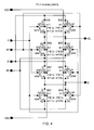
- Figure 4 is a detailed schematic diagram of the transmission gate.
- the control signal P/XP either the non-inverting input D or the inverting input XD is connected respectively to the inverted output Q or the inverted output XQ.
- the first polarity-control cell POL3 is arranged to receive the sampling clock signal CLK and has its non-inverted output Q connected to the non-inverting clock input CLK of the first sampling circuitry portion DFF3.
- the first polarity-control cell POL3 is arranged to feed an inverted version of the sampling clock signal CLK to the non-inverting clock input CLK of the first sampling circuitry portion DFF3.
- the first polarity-control cell POL3 serves to match a delay in the signal path that feeds the sampling clock signal CLK to the first sampling circuitry portion DFF3 with a delay in a signal path that feeds the sampling clock signal CLK to the second sampling circuitry portion DFF4.
- a non-inverting control input P of the first polarity-control cell POL3 is tied to VDD, and is therefore set to logic 1.
- the second polarity-control cell POL4 is arranged to receive the sampling clock signal CLK and has its non-inverted output Q connected to a non-inverting clock input CLK of the second sampling circuitry portion DFF4.
- the second polarity-control cell DFF4 is arranged to feed an inverted or a non-inverted version of the sampling clock signal CLK to the non-inverting clock input CLK of the second sampling circuitry portion DFF4 according to a level of a sampling frequency selection signal, B.
- the second polarity-control cell POL4 is arranged to receive the sampling frequency selection signal B at its non-inverting control input P.
- the arrangement allows the phase-error-reduction circuitry 30 to adjust a frequency at which the I and Q input signals are sampled in response to a level of the sampling frequency selection signal B.
- the phase-error-reduction circuitry 30 is arranged to sample the I and Q input signals at a frequency which is an even multiple of the IQ generator clock signal DCLK in response to the sampling frequency selection signal B being at a first level corresponding to logic 1 and to sample the I and Q input signals at a frequency which is an odd multiple of the IQ generator clock signal DCLK in response to the sampling frequency selection signal B being at a second level corresponding to logic 0.
- phase-error-reduction circuitry 30 will now be described with reference to the timing diagrams in Figures 5 and 6 .
- Figure 5 shows the IQ generator clock signal DCLK, the I input signal (I i/p), the Q input signal (Q i/p), the sampling clock signal CLK, the I output signal (I o/p) and the Q output signal (Q o/p).
- the control input P of the first polarity- control cell POL3 is tied to logic 1
- the first sampling circuitry portion DFF3 samples on the falling edge of the sampling clock signal CLK.
- Setting B to logic 1 gives an even ratio between the sampling clock signal CLK and the IQ generator clock signal DCLK (in this configuration, the ratio is two).
- the second polarity-control cell POL4 inverts the sampling clock signal CLK. This means that the second sampling circuitry portion DFF4 also samples on the falling edge of the sampling clock signal CLK.
- the Q input signal in Figure 5 has a phase difference to the I input signal which is less than 90°, with the Q input signal rising at time t 1 rather than at the correct time t 2 .
- the timing diagram demonstrates that, by sampling the I and Q input signals (in this case on the falling edge of the sampling clock signal CLK), the phase error between the I and Q output signals is reduced.
- FIG. 6 shows a similar example in which there is an odd ratio between the sampling clock signal CLK and the IQ generator clock signal DCLK (in this configuration, the ratio is three).
- B is set to logic 0, which means that DFF4 samples on a rising edge of the sampling clock signal CLK (while the first sampling circuitry portion DFF3 still samples on the falling edge of the sampling clock signal CLK). The phase error between the I and Q output signals is again reduced.
- FIG 7 shows a phase-controlled IQ generator 100 arranged to output I and Q signals.
- the phase-controlled IQ generator 100 is based on the IQ generator 10 shown in Figure 1 and comprises phase control circuitry 150 arranged to switch the phase relationship of the I and Q signals between the I signal leading the Q signal and the I signal lagging the Q signal in response to a phase relationship selection signal S.
- the phase control circuitry 150 comprises first and second polarity-control cells POL1 and POL2 arranged to output an inverted or a non-inverted version of their input signals according to a level of the phase relationship selection signal S.
- the first and second polarity control cells POL1 and POL2 are transmission gates as shown in Figure 4 .
- the phase-controlled IQ generator 100 comprises a master latch circuitry portion DFF1, a slave latch circuitry portion DFF2 and the first and second polarity-control cells POL1 and POL2.
- the master latch circuitry portion DFF1 is arranged to receive an IQ generator clock signal DCLK at its non-inverting clock input CLK and the slave latch circuitry portion DFF2 is arranged to receive the IQ generator clock signal DCLK at its inverting clock input XCLK.
- the master latch circuitry portion DFF1 is arranged to receive at a non-inverting input a signal from the inverted output of the slave latch circuitry portion DFF2 via the first polarity-control cell POL1.
- the slave latch circuitry portion DFF2 is arranged to receive at a non-inverting input a signal from the non-inverted output of the master latch circuitry portion DFF1 via the second polarity-control cell POL2.
- phase-controlled IQ generator 100 The operation of the phase-controlled IQ generator 100 will now be described with reference to the timing diagrams in Figures 8 and 9 .
- the purpose of the polarity-control cells POL1 and POL2 is to invert the input signals of the master and slave latch circuitry DFF1 and DFF2.
- the master latch circuitry portion DFF1 latches on the rising edge of the IQ generator clock signal DCLK and the slave latch circuitry portion DFF2 samples on the falling edge of the IQ generator clock signal DCLK.
- the inverted output XQ of the slave latch circuitry portion DFF2 is connected to the non-inverting input D of the first polarity-control cell POL1, the signal is inverted.
- FIG 8 shows the case in which the phase relationship selection signal S is at logic 0.
- the polarity-control cells POL1 and POL2 do not invert the signal.
- the Q signal is initially logic 0.
- the non-inverting input D of the master latch circuitry portion DFF1 receives the inverted output XQ of the slave latch circuitry portion DFF2, and therefore receives a signal at logic 1.
- the I signal With the next rising edge of the IQ generator clock signal DCLK, the I signal will be at logic 1.
- the following falling edge of the IQ generator clock signal DCLK sets the Q signal to logic 1, and so on. This means the I signal is in front of the Q signal.
- FIG. 9 shows the case in which the phase relationship selection signal S is at logic 1.
- both polarity-control cells POL1 and POL2 invert their signals.
- the signal from the inverted output XQ of the slave latch circuitry portion DFF2 is inverted by the first polarity-control cell POL1, which has the same effect as if the master slave latch circuitry portion DFF1 received a signal from the non-inverted output of the slave latch circuitry portion DFF2, i.e. the Q signal.
- the Q signal was logic 1 and is now logic 0, when the master latch circuitry portion DFF1 latches on the rising edge of the IQ generator clock signal DCLK, the I signal will change to logic 0.
- the following falling edge of the IQ generator clock signal DCLK sets the Q signal to logic 1 as the slave latch circuitry portion DFF2 latches an inverted version of the I signal (inverted by the second polarity-control cell POL2). With the next rising edge of the IQ generator clock signal DCLK, the master latch circuitry portion DFF1 latches the Q signal, which is at logic 1. The I signal will be therefore also be logic 1. This means the I signals is behind the Q signal.
- Figure 10 shows an IQ generator 200 including the phase control circuitry 150 of Figure 7 and being connected to the phase-error-reduction circuitry 30 of Figure 3 .
- the operation of the phase control circuitry 150 and the phase-error-reduction circuitry 30 is as described above.
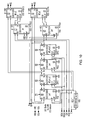
- Figure 11 is a schematic diagram of evaluation circuitry suitable for evaluating the phase error of an IQ generator.
- the outputs of the IQ generator are connected over ideal comparators to an ideal mixer.
- the output voltage of the mixer will be converted to current using a voltage controlled current source connected over a DC source to ground.
- the magnitude of the generated current gives the relative phase error.
- phase error In order to have a reference value for the phase error both inputs of the mixer have to be connected to the same comparator output i.e. Idiff. This corresponds to a phase error of 90°.
- the magnitude of the generated current can be used as reference.
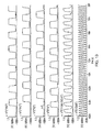
- Figures 12 to 15 are graphs showing the results of simulations of the IQ generator of Figure 10 in various configurations.
- Figure 12 shows the results for a configuration in which both the sampling frequency selection signal and the phase relationship selection signal are at logic 0.
- Figure 13 shows the results for a configuration in which the sampling frequency selection signal is at logic 1 and the phase relationship selection signal is at logic 0.
- Figure 14 shows the results for a configuration in which the sampling frequency selection signal is at logic 0 and the phase relationship selection signal is at logic 1.
- Figure 15 shows the results for a configuration in which both the sampling frequency selection signal and the phase relationship selection signal are at logic 1.
- Table 1 below indicates the settings used in the simulations and their significance.
- Figure 16 is a flowchart representing a method of reducing a phase error between I and Q signals from an IQ generator.
- the method comprises receiving (1002) I and Q input signals from the IQ generator and producing (1004) I and Q output signals, and wherein producing the I and Q output signals comprises sampling the I and Q input signals to tend to reduce a phase error between the I and Q output signals.
- Figure 17 is a flowchart representing a method of operating a phase-controlled IQ generator comprising outputting (2002) I and Q signals and switching (2004) the phase relationship of the I and Q signals between the I signal leading the Q signal and the 3 signal lagging the Q signal in response to a phase relationship selection signal.
- sampling/latch circuitry may be used instead of other forms of sampling/latch circuitry.
- a JK flip-flop configured as a D-type flip-flop may be used.
- circuitry may have other functions in addition to the mentioned functions, and that these functions may be performed by the same circuit.
Landscapes
- Physics & Mathematics (AREA)
- Nonlinear Science (AREA)
- Stabilization Of Oscillater, Synchronisation, Frequency Synthesizers (AREA)
- Manipulation Of Pulses (AREA)
- Synchronisation In Digital Transmission Systems (AREA)
Abstract
Description
- The invention relates to phase-error-reduction circuitry for an IQ generator and to a phase-controlled IQ generator.
- The purpose of an IQ generator is to generate 90° phase-shifted signals I and Q.
-
Figure 1 shows anIQ generator 10 including a master flip-flop DFF1 and a slave flip-flop DFF2. A clock signal DCLK is fed to a non-inverting clock input CLK of the master flip-flop DFF1 and to an inverting clock input XCLK of the slave flip-flop DFF2. A non-inverted output Q of the master flip-flop DFF1 is fed to a non-inverting input D of the slave flip-flop DFF2. An inverted output XQ of the slave flip-flop DFF2 is fed back to a non-inverting input D of the master flip-flop DFF1. The non-inverted output Q of the master flip-flop DFF1 produces an I signal and a non-inverted output Q of the slave flip-flop DFF2 produces a Q signal, which lags the I signal by approximately 90°. Owing for example to signal path mismatches in the circuit, the phase lag may not be exactly 90°. - According to a first aspect, there is provided phase-error-reduction circuitry for an IQ generator, wherein the phase-error-reduction circuitry is arranged to receive I and Q input signals from the IQ generator and to produce I and Q output signals, and wherein the phase-error-reduction circuitry is arranged to sample the I and Q input signals to tend to reduce a phase error between the I and Q output signals.
- In one embodiment, the phase-error-reduction circuitry is arranged to sample the I and Q input signals and reduce the phase error between the I and Q output signals. In another embodiment, the phase-error-reduction circuitry is arranged to sample the I and Q input signals so as to reduce a phase error between the I and Q output signals. In another embodiment, the phase-error-reduction circuitry is arranged to sample the I and Q input signals to tend to synchronise the I and Q output signals. In another embodiment, the phase-error-reduction circuitry is arranged to sample the I and Q input signals and synchronise the I and Q output signals. In another embodiment, the phase-error-reduction circuitry is arranged to sample the I and Q input signals so as to synchronise the I and Q output signals.
- The phase-error-reduction circuitry may comprise first and second sampling circuitry portions arranged to receive the respective I and Q input signals and to produce the respective I and Q output signals, wherein the first and second sampling circuitry portions are arranged to sample the respective I and Q input signals according to a sampling clock signal, the sampling clock signal being independent of an IQ generator clock signal of the IQ generator.
- The IQ generator clock signal may be derived from the sampling clock signal, for example by inputting the sampling clock signal to a divider and obtaining the IQ generator clock signal from the output of the divider. In a variant, the sampling clock signal may be derived from the IQ generator clock signal, for example by using a phase locked loop or a clock multiplier. In any case, both the sampling clock signal and the IQ generator clock signal should have a duty cycle which is as close to 50/50 as possible.
- The phase-error-reduction circuitry may be arranged to adjust a frequency at which the I and Q input signals are sampled in response to a level of a sampling frequency selection signal.
- The phase-error-reduction circuitry may be arranged to sample the I and Q input signals at a frequency which is an even multiple of an IQ generator clock signal in response to the sampling frequency selection signal being at a first level and to sample the I and Q input signals at a frequency which is an odd multiple of the IQ generator clock signal in response to the sampling frequency selection signal being at a second level.
- Such an arrangement may be used in conjunction with a voltage-controlled oscillator to generate the sampling clock signal and, depending on the required frequency, a fixed ratio divider or a programmable divider with odd or even ratios to derive the IQ generator clock signal from the sampling clock signal.
- The phase-error-reduction circuitry may comprise a polarity-control cell arranged to receive the sampling clock signal and having its output connected to a clock input of one of the first and second sampling circuitry portions, the polarity-control cell being arranged to feed an inverted or a non-inverted version of the sampling clock signal to the clock input of the respective sampling circuitry portion according to a level of a sampling frequency selection signal.
- The phase-error-reduction circuitry may comprise a further poiarity-control cell arranged to receive the sampling clock signal and having its output connected to a clock input of the other of the first and second sampling circuitry portions, the further polarity-control cell being arranged to feed an inverted version of the sampling clock signal to the clock input of the respective sampling circuitry portion.
- The first and second sampling circuitry portions may be arranged to sample the I and Q input signals on one of a rising edge and a falling edge of the sampling clock signal.
- One of the first and second sampling circuitry portions may be arranged to sample the respective I or Q input signal on a rising edge of the sampling clock signal and the other of the first and second sampling circuitry portions is arranged to sample the respective I or Q input signal on a falling edge of the sampling clock signal.
- A frequency of a sampling clock signal may be at least four times higher than a frequency of the I and Q output signals.
- According to a second aspect, there is provided a phase-controlled IQ generator arranged to output I and Q signals and comprising phase control circuitry arranged to switch the phase relationship of the I and Q signals between the I signal leading the Q signal and the I signal lagging the Q signal in response to a phase relationship selection signal.
- The ability to control the phase relationship of the I and Q signals in this manner may provide for the selection of the upper and lower sideband in the conversion of the RF signals.
- The phase control circuitry may comprise at least one polarity-control cell arranged to output an inverted or a non-inverted version of its input signal according to a level of the phase relationship selection signal.
- The phase-controlled IQ generator may comprise a master latch circuitry portion and a slave latch circuitry portion, wherein the phase control circuitry is arranged to invert or not to invert inputs to the master and slave latch circuitry portions according to a level of the phase relationship selection signal.
- The phase-controlled IQ generator may comprise a master latch circuitry portion, a slave latch circuitry portion and first and second polarity-control cells, the master latch circuitry portion being arranged to receive an IQ generator clock signal at its non-inverting clock input and the slave latch circuitry portion being arranged to receive the IQ generator clock signal at its inverting clock input, the master latch circuitry portion being arranged to receive at a non-inverting input a signal from the inverted output of the slave latch circuitry portion via the first polarity-control cell, and the slave latch circuitry portion being arranged to receive at a non-inverting input a signal from the non-inverted output of the master latch circuitry portion via the second polarity-control cell, wherein each of the first and second polarity control cells is arranged to receive the phase relationship selection signal and to output an inverted or a non-inverted version of its input signal according to a level of the phase relationship selection signal.
- The phase-controlled IQ generator of the second aspect may be connected to the phase-error-reduction circuitry of the first aspect such that the I and Q signals output by the phase-controlled IQ generator are received by the phase-error-reduction circuitry as the I and Q input signals.
- In the phase-error-reduction circuitry of the first aspect, the IQ generator may comprise the phase-controlled IQ generator of the second aspect.
- According to a third aspect, there is provided a phase-controlled IQ generator arranged to output I and Q signals and comprising phase control circuitry arranged to switch the phase relationship of the I and Q signals between the I signal leading the Q signal and the I signal lagging the Q signal in response to a phase relationship selection signal, wherein the phase-controlled IQ generator is connected to phase-error-reduction circuitry arranged to receive the I and Q signals from the phase-controlled IQ generator as I and Q input signals and to produce I and Q output signals, and wherein the phase-error-reduction circuitry is arranged to sample the I and Q input signals to tend to reduce a phase error between the I and Q output signals.
- According to a fourth aspect, there is provided a method of reducing a phase error between I and Q signals from an IQ generator, the method comprising receiving I and Q input signals from the IQ generator and producing I and Q output signals, and wherein producing the I and Q output signals comprises sampling the I and Q input signals to tend to reduce a phase error between the I and Q output signals.
- According to a fifth aspect, there is provided a method of operating a phase-controlled IQ generator comprising outputting I and Q signals and switching the phase relationship of the I and Q signals between the I signal leading the Q signal and the I signal lagging the Q signal in response to a phase relationship selection signal.
- According to a sixth aspect, there is provided means for reducing a phase error between I and Q signals from an IQ generator, wherein the means for reducing a phase error is arranged to receive I and Q input signals from the IQ generator and to produce I and Q output signals, and wherein the means for reducing a phase error is arranged to sample the I and Q input signals to tend to reduce a phase error between the I and Q output signals.
- According to a seventh aspect, there is provided means for outputting I and Q signals comprising means for controlling a phase relationship arranged to switch the phase relationship of the I and Q signals between the I signal leading the Q signal and the I signal lagging the Q signal in response to a phase relationship selection signal.
- According to a eighth aspect, there is provided a method of reducing a phase error between I and Q signals from an IQ generator, the method comprising the steps of receiving I and Q input signals from the IQ generator and producing I and Q output signals, and wherein the step of producing the I and Q output signals comprises the step of sampling the I and Q input signals to tend to reduce a phase error between the I and Q output signals.
- According to a ninth aspect, there is provided a method of operating a phase-controlled IQ generator comprising the steps of outputting I and Q signals and switching the phase relationship of the I and Q signals between the I signal leading the Q signal and the I signal lagging the Q signal in response to a phase relationship selection signal.
- The present invention includes one or more aspects, embodiments or features in isolation or in various combinations whether or not specifically stated (including claimed) in that combination or in isolation.
- The above summary is intended to be merely exemplary and non-limiting.
- A description is now given, by way of example only, with reference to the accompanying drawings, in which:-
-
Figure 1 is a schematic diagram of an IQ generator; -
Figure 2 is a schematic diagram showing the IQ generator ofFigure 1 connected to phase-error-reduction circuitry; -
Figure 3 is a schematic diagram showing the IQ generator ofFigure 1 connected to a variant of the phase-error-reduction circuitry ofFigure 2 ; -
Figure 4 . is a schematic diagram of a polarity-control cell of the phase-error-reduction circuitry ofFigure 3 ; -
Figure 5 is a timing diagram illustrating one mode of operation of the phase-error-reduction circuitry ofFigure 3 ; -
Figure 6 is a timing diagram illustrating another mode of operation of the phase-error-reduction circuitry ofFigure 3 ; -
Figure 7 is a schematic diagram of a phase-controlled IQ generator including phase control circuitry; -
Figure 8 is a timing diagram illustrating one mode of operation of the phase-controlled IQ generator ofFigure 7 ; -
Figure 9 is a timing diagram illustrating another mode of operation of the phase-controlled IQ generator ofFigure 7 ; -
Figure 10 is a schematic diagram of an IQ generator including the phase control circuitry ofFigure 7 and being connected to the phase-error-reduction circuitry ofFigure 3 ; -
Figure 11 is a schematic diagram of evaluation circuitry suitable for evaluating the phase error of an IQ generator; -
Figure 12 is a graph showing the results of a simulation of the IQ generator ofFigure 10 in one configuration; -
Figure 13 is a graph showing the results of a simulation of the IQ generator ofFigure 10 in another configuration; -
Figure 14 is a graph showing the results of a simulation of the IQ generator ofFigure 10 in another configuration; -
Figure 15 is a graph showing the results of a simulation of the IQ generator ofFigure 10 in another configuration; -
Figure 16 is a flowchart representing a method of reducing a phase error between I and Q signals from an IQ generator; -
Figure 17 is a flowchart representing a method of operating a phase-controlled IQ generator. - Throughout the following description, where a signal is fed to one of an inverting input and a non-inverting input, the complement of the signal is fed to the other of the inverting input and the non-inverting input. Reference may be made to only one of the signals. It should be understood that such an arrangement is optional.
-
Figure 2 shows theIQ generator 10 ofFigure 1 connected to phase-error-reduction circuitry 20. - The
IQ generator 10 includes a master latch circuitry portion DFF1 and a slave latch circuitry portion DFF2. Although each of the master and slave latch circuitry portions DFF1 and DFF2 is shown in the form of a D-type flip-flop, it is to be understood that other types of latch circuitry may be used. An IQ generator clock signal DCLK is fed to a non-inverting clock input CLK of the master latch circuitry portion DFF1 and to an inverting clock input XCLK of the slave latch circuitry portion DFF2. A non-inverted output Q of the master latch circuitry portion DFF1 is fed to a non-inverting input D of the slave latch circuitry portion DFF2. An inverted output XQ of the slave latch circuitry portion DFF2 is fed back to a non-inverting input D of the master latch circuitry portion DFF1. - The phase-error-
reduction circuitry 20 includes a first sampling circuitry portion DFF3 and a second sampling circuitry portion DFF4. in this embodiment, each of the first and second sampling circuitry portions DFF3 and DFF4 comprises a D-type flip-flop. A non-inverting input D of the first sampling circuitry portion DFF3 is arranged to receive an I input signal from the non-inverted output Q of the master latch circuitry portion DFF1 of theIQ generator 10. A non-inverting input D of the second sampling circuitry portion DFF4 is arranged to receive a Q input signal from the non-inverted output Q of the slave latch circuitry portion DFF2 of theIQ generator 10. A non-inverted output Q of the first sampling circuitry portion DFF3 produces an I output signal and a non-inverted output Q of the second sampling circuitry portion DFF4 produces a Q output signal. A sampling clock signal CLK is fed to the non-inverting clock input CLK of each of the first and second sampling circuitry portions DFF3 and DFF4. A frequency of the sampling clock signal CLK is at least two times, and is an integer multiple of, a frequency of the IQ generator clock signal DCLK. Each of the first and second sampling circuitry portions DFF3 DFF4 is arranged to sample the respective I and Q input signal on a rising edge of the sampling clock signal CLK. - In a variant, the frequency of the sampling clock signal CLK may be a non-integer multiple of the frequency of the IQ generator clock signal DCLK. For example, a fractional divider with a multi-modulus approach may be used.
- In use, the
IQ generator 10 produces the I and Q input signals for the phase-error-reduction circuitry 20. There may be a phase error between the I and Q input signals, such that the phase lag between the signals is not exactly 90°. By sampling the I and Q input signals, the phase-error-reduction circuitry 20 tends to reduce the phase error between the I and Q output signals. - Any phase error between the I output signal and the IQ generator clock signal DCLK or between the Q output signal and the IQ generator clock signal is not important.
-
Figure 3 shows theIQ generator 10 ofFigure 1 connected to phase-error-reduction circuitry 30, which is a variant of the phase-error-reduction circuitry 20 ofFigure 2 . - The phase-error-reduction circuitry 30 includes first and second sampling circuitry portions DFF3 and DFF4, the purpose and function of which is identical to those of phase-error-
reduction circuitry 20 shown inFigure 2 . - Phase-error-reduction circuitry 30 differs from phase-error-
reduction circuitry 20 in that the sampling clock signal CLK is not fed directly to the non-inverting clock inputs CLK of the first and second sampling circuitry portions DFF3 and DFF4, but is passed via respective first and second polarity-control cells POL3 and POL4. - In this embodiment, each of the first and second polarity-control cells POL3 and POL4 comprises a transmission gate.
Figure 4 is a detailed schematic diagram of the transmission gate. Depending on the control signal P/XP, either the non-inverting input D or the inverting input XD is connected respectively to the inverted output Q or the inverted output XQ. - Referring back to
Figure 3 , the first polarity-control cell POL3 is arranged to receive the sampling clock signal CLK and has its non-inverted output Q connected to the non-inverting clock input CLK of the first sampling circuitry portion DFF3. The first polarity-control cell POL3 is arranged to feed an inverted version of the sampling clock signal CLK to the non-inverting clock input CLK of the first sampling circuitry portion DFF3. The first polarity-control cell POL3 serves to match a delay in the signal path that feeds the sampling clock signal CLK to the first sampling circuitry portion DFF3 with a delay in a signal path that feeds the sampling clock signal CLK to the second sampling circuitry portion DFF4. A non-inverting control input P of the first polarity-control cell POL3 is tied to VDD, and is therefore set tologic 1. - The second polarity-control cell POL4 is arranged to receive the sampling clock signal CLK and has its non-inverted output Q connected to a non-inverting clock input CLK of the second sampling circuitry portion DFF4. The second polarity-control cell DFF4 is arranged to feed an inverted or a non-inverted version of the sampling clock signal CLK to the non-inverting clock input CLK of the second sampling circuitry portion DFF4 according to a level of a sampling frequency selection signal, B. The second polarity-control cell POL4 is arranged to receive the sampling frequency selection signal B at its non-inverting control input P.
- The arrangement allows the phase-error-reduction circuitry 30 to adjust a frequency at which the I and Q input signals are sampled in response to a level of the sampling frequency selection signal B. The phase-error-reduction circuitry 30 is arranged to sample the I and Q input signals at a frequency which is an even multiple of the IQ generator clock signal DCLK in response to the sampling frequency selection signal B being at a first level corresponding to
logic 1 and to sample the I and Q input signals at a frequency which is an odd multiple of the IQ generator clock signal DCLK in response to the sampling frequency selection signal B being at a second level corresponding to logic 0. - The operation of the phase-error-reduction circuitry 30 will now be described with reference to the timing diagrams in
Figures 5 and6 . -
Figure 5 shows the IQ generator clock signal DCLK, the I input signal (I i/p), the Q input signal (Q i/p), the sampling clock signal CLK, the I output signal (I o/p) and the Q output signal (Q o/p). As the control input P of the first polarity- control cell POL3 is tied tologic 1, the first sampling circuitry portion DFF3 samples on the falling edge of the sampling clock signal CLK. Setting B tologic 1 gives an even ratio between the sampling clock signal CLK and the IQ generator clock signal DCLK (in this configuration, the ratio is two). As a result of this setting, the second polarity-control cell POL4 inverts the sampling clock signal CLK. This means that the second sampling circuitry portion DFF4 also samples on the falling edge of the sampling clock signal CLK. - To illustrate the operation of the phase-error-reduction circuitry 30, the Q input signal in
Figure 5 has a phase difference to the I input signal which is less than 90°, with the Q input signal rising at time t1 rather than at the correct time t2. The timing diagram demonstrates that, by sampling the I and Q input signals (in this case on the falling edge of the sampling clock signal CLK), the phase error between the I and Q output signals is reduced. -
Figure 6 shows a similar example in which there is an odd ratio between the sampling clock signal CLK and the IQ generator clock signal DCLK (in this configuration, the ratio is three). In this case, B is set to logic 0, which means that DFF4 samples on a rising edge of the sampling clock signal CLK (while the first sampling circuitry portion DFF3 still samples on the falling edge of the sampling clock signal CLK). The phase error between the I and Q output signals is again reduced. -
Figure 7 shows a phase-controlledIQ generator 100 arranged to output I and Q signals. The phase-controlledIQ generator 100 is based on theIQ generator 10 shown inFigure 1 and comprisesphase control circuitry 150 arranged to switch the phase relationship of the I and Q signals between the I signal leading the Q signal and the I signal lagging the Q signal in response to a phase relationship selection signal S. - The
phase control circuitry 150 comprises first and second polarity-control cells POL1 and POL2 arranged to output an inverted or a non-inverted version of their input signals according to a level of the phase relationship selection signal S. in this embodiment, the first and second polarity control cells POL1 and POL2 are transmission gates as shown inFigure 4 . - The phase-controlled
IQ generator 100 comprises a master latch circuitry portion DFF1, a slave latch circuitry portion DFF2 and the first and second polarity-control cells POL1 and POL2. The master latch circuitry portion DFF1 is arranged to receive an IQ generator clock signal DCLK at its non-inverting clock input CLK and the slave latch circuitry portion DFF2 is arranged to receive the IQ generator clock signal DCLK at its inverting clock input XCLK. The master latch circuitry portion DFF1 is arranged to receive at a non-inverting input a signal from the inverted output of the slave latch circuitry portion DFF2 via the first polarity-control cell POL1. The slave latch circuitry portion DFF2 is arranged to receive at a non-inverting input a signal from the non-inverted output of the master latch circuitry portion DFF1 via the second polarity-control cell POL2. - The operation of the phase-controlled
IQ generator 100 will now be described with reference to the timing diagrams inFigures 8 and9 . - The purpose of the polarity-control cells POL1 and POL2 is to invert the input signals of the master and slave latch circuitry DFF1 and DFF2. The master latch circuitry portion DFF1 latches on the rising edge of the IQ generator clock signal DCLK and the slave latch circuitry portion DFF2 samples on the falling edge of the IQ generator clock signal DCLK. As the inverted output XQ of the slave latch circuitry portion DFF2 is connected to the non-inverting input D of the first polarity-control cell POL1, the signal is inverted.
-
Figure 8 shows the case in which the phase relationship selection signal S is at logic 0. In this case, the polarity-control cells POL1 and POL2 do not invert the signal. It can be seen that the Q signal is initially logic 0. The non-inverting input D of the master latch circuitry portion DFF1 receives the inverted output XQ of the slave latch circuitry portion DFF2, and therefore receives a signal atlogic 1. With the next rising edge of the IQ generator clock signal DCLK, the I signal will be atlogic 1. The following falling edge of the IQ generator clock signal DCLK sets the Q signal tologic 1, and so on. This means the I signal is in front of the Q signal. -
Figure 9 shows the case in which the phase relationship selection signal S is atlogic 1. In this case, both polarity-control cells POL1 and POL2 invert their signals. The signal from the inverted output XQ of the slave latch circuitry portion DFF2 is inverted by the first polarity-control cell POL1, which has the same effect as if the master slave latch circuitry portion DFF1 received a signal from the non-inverted output of the slave latch circuitry portion DFF2, i.e. the Q signal. Assuming that, in earlier states, the Q signal waslogic 1 and is now logic 0, when the master latch circuitry portion DFF1 latches on the rising edge of the IQ generator clock signal DCLK, the I signal will change to logic 0. The following falling edge of the IQ generator clock signal DCLK sets the Q signal tologic 1 as the slave latch circuitry portion DFF2 latches an inverted version of the I signal (inverted by the second polarity-control cell POL2). With the next rising edge of the IQ generator clock signal DCLK, the master latch circuitry portion DFF1 latches the Q signal, which is atlogic 1. The I signal will be therefore also belogic 1. This means the I signals is behind the Q signal. -
Figure 10 shows an IQ generator 200 including thephase control circuitry 150 ofFigure 7 and being connected to the phase-error-reduction circuitry 30 ofFigure 3 . The operation of thephase control circuitry 150 and the phase-error-reduction circuitry 30 is as described above. -
Figure 11 is a schematic diagram of evaluation circuitry suitable for evaluating the phase error of an IQ generator. - The outputs of the IQ generator are connected over ideal comparators to an ideal mixer. The output voltage of the mixer will be converted to current using a voltage controlled current source connected over a DC source to ground. The magnitude of the generated current gives the relative phase error.
- In order to have a reference value for the phase error both inputs of the mixer have to be connected to the same comparator output i.e. Idiff. This corresponds to a phase error of 90°. The magnitude of the generated current can be used as reference. The formula to calculate the phase error can be expressed as:-

-
Figures 12 to 15 are graphs showing the results of simulations of the IQ generator ofFigure 10 in various configurations. -
Figure 12 shows the results for a configuration in which both the sampling frequency selection signal and the phase relationship selection signal are at logic 0. -
Figure 13 shows the results for a configuration in which the sampling frequency selection signal is atlogic 1 and the phase relationship selection signal is at logic 0. -
Figure 14 shows the results for a configuration in which the sampling frequency selection signal is at logic 0 and the phase relationship selection signal is atlogic 1. -
Figure 15 shows the results for a configuration in which both the sampling frequency selection signal and the phase relationship selection signal are atlogic 1. - Table 1 below indicates the settings used in the simulations and their significance.
Table 1 S Description B Description 0 I 90 deg in front of Q 0 odd ratio between CLK and DCLK 1 I 90 deg behind Q 1 even ratio between CLK and DCLK -
Figure 16 is a flowchart representing a method of reducing a phase error between I and Q signals from an IQ generator. The method comprises receiving (1002) I and Q input signals from the IQ generator and producing (1004) I and Q output signals, and wherein producing the I and Q output signals comprises sampling the I and Q input signals to tend to reduce a phase error between the I and Q output signals. -
Figure 17 is a flowchart representing a method of operating a phase-controlled IQ generator comprising outputting (2002) I and Q signals and switching (2004) the phase relationship of the I and Q signals between the I signal leading the Q signal and the 3 signal lagging the Q signal in response to a phase relationship selection signal. - Although the above embodiments have been described using D-type flip-flops at the sampling/latch circuitry portions, it will be understood that other forms of sampling/latch circuitry may be used instead. For example, in one variant, a JK flip-flop configured as a D-type flip-flop may be used.
- It will be appreciated that the aforementioned circuitry may have other functions in addition to the mentioned functions, and that these functions may be performed by the same circuit.
- The applicant hereby discloses in isolation each individual feature described herein and any combination of two or more such features, to the extent that such features or combinations are capable of being carried out based on the present specification as a whole in the light of the common general knowledge of a person skilled in the art, irrespective of whether such features or combinations of features solve any problems disclosed herein, and without limitation to the scope of the claims. The applicant indicates that aspects of the present invention may consist of any such individual feature or combination of features. In view of the foregoing description it will be evident to a person skilled in the art that various modifications may be made within the scope of the invention.
- While there have been shown and described and pointed out fundamental novel features of the invention as applied to preferred embodiments thereof, it will be understood that various omissions and substitutions and changes in the form and details of the devices and methods described may be made by those skilled in the art without departing from the spirit of the invention. For example, it is expressly intended that all combinations of those elements and/or method steps which perform substantially the same function in substantially the same way to achieve the same results are within the scope of the invention. Moreover, it should be recognized that structures and/or elements and/or method steps shown and/or described in connection with any disclosed form or embodiment of the invention may be incorporated in any other disclosed or described or suggested form or embodiment as a general matter of design choice. It is the intention, therefore, to be limited only as indicated by the scope of the claims appended hereto. Furthermore, in the claims means-plus-function clauses are intended to cover the structures described herein as performing the recited function and not only structural equivalents, but also equivalent structures. Thus although a nail and a screw may not be structural equivalents in that a nail employs a cylindrical surface to secure wooden parts together, whereas a screw employs a helical surface, in the environment of fastening wooden parts, a nail and a screw may be equivalent structures.
Claims (18)
- Phase-error-reduction circuitry (20;30) for an IQ generator (10; 100; 200), wherein the phase-error-reduction circuitry is arranged to receive I and Q input signals from the IQ generator and to produce I and Q output signals, and wherein the phase-error-reduction circuitry is arranged to sample the I and Q input signals to tend to reduce a phase error between the I and Q output signals.
- The phase-error-reduction circuitry of claim 1 comprising first and second sampling circuitry portions (DFF3, DFF4) arranged to receive the respective I and Q input signals and to produce the respective I and Q output signals, wherein the first and second sampling circuitry portions are arranged to sample the respective I and Q input signals according to a sampling clock signal (CLK), the sampling clock signal being independent of an IQ generator clock signal (DCLK) of the IQ generator (10; 100; 200).
- The phase-error-reduction circuitry of any preceding claim arranged to adjust a frequency at which the I and Q input signals are sampled in response to a level of a sampling frequency selection signal (B).
- The phase-error-reduction circuitry of claim 3 arranged to sample the I and Q input signals at a frequency which is an even multiple of an IQ generator clock signal (DCLK) in response to the sampling frequency selection signal (B) being at a first level and to sample the I and Q input signals at a frequency which is an odd multiple of the IQ generator clock signal in response to the sampling frequency selection signal being at a second level.
- The phase-error-reduction circuitry of claim 2 comprising a polarity-control cell (POL4) arranged to receive the sampling clock signal (CLK) and having its output connected to a clock input of one of the first and second sampling circuitry portions (DFF3, DFF4), the polarity-control cell being arranged to feed an inverted or a non-inverted version of the sampling clock signal to the clock input of the respective sampling circuitry portion according to a level of a sampling frequency selection signal (B).
- The phase-error-reduction circuitry of claim 5 comprising a further polarity-control cell (POL3) arranged to receive the sampling clock signal (CLK) and having its output connected to a clock input of the other of the first and second sampling circuitry portions (DFF3, DFF4), the further polarity-control cell being arranged to feed an inverted version of the sampling clock signal to the clock input of the respective sampling circuitry portion.
- The phase-error-reduction circuitry of claim 2 wherein the first and second sampling circuitry portions (DFF3, DFF4) are arranged to sample the I and Q input signals on one of a rising edge and a falling edge of the sampling clock signal (CLK).
- The phase-error-reduction circuitry of claim 2 wherein one of the first and second sampling circuitry portions (DFF3, DFF4) is arranged to sample the respective I or Q input signal on a rising edge of the sampling clock signal (CLK) and the other of the first and second sampling circuitry portions is arranged to sample the respective I or Q input signal on a falling edge of the sampling clock signal.
- The phase-error-reduction circuitry of any preceding claim wherein a frequency of a sampling clock signal (CLK) is at least four times higher than a frequency of the I and Q output signals.
- A phase-controlled IQ generator (100; 200) arranged to output I and Q signals and comprising phase control circuitry (150) arranged to switch the phase relationship of the I and Q signals between the I signal leading the Q signal and the I signal lagging the Q signal in response to a phase relationship selection signal (S).
- The phase-controlled IQ generator of claim 10 wherein the phase control circuitry (150) comprises at least one polarity-control cell (POL1, POL2) arranged to output an inverted or a non-inverted version of its input signal according to a level of the phase relationship selection signal (S).
- The phase-controlled IQ generator of claim 10 or 11 comprising a master latch circuitry portion (DFF1) and a slave latch circuitry portion (DFF2), wherein the phase control circuitry (150) is arranged to invert or not to invert inputs to the master and slave latch circuitry portions according to a level of the phase relationship selection signal (S).
- The phase-controlled IQ generator of any of claims 10 to 12 comprising a master latch circuitry portion (DFF1), a slave latch circuitry portion (DFF2) and first and second polarity-control cells (POL1, POL2), the master latch circuitry portion being arranged to receive an IQ generator clock signal (DCLK) at its non-inverting clock input and the slave latch circuitry portion being arranged to receive the IQ generator clock signal at its inverting clock input, the master latch circuitry portion being arranged to receive at a non-inverting input a signal from the inverted output of the slave latch circuitry portion via the first polarity-control cell, and the slave latch circuitry portion being arranged to receive at a non-inverting input a signal from the non-inverted output of the master latch circuitry portion via the second polarity-control cell, wherein each of the first and second polarity control cells is arranged to receive the phase relationship selection signal (S) and to output an inverted or a non-inverted version of its input signal according to a level of the phase relationship selection signal.
- The phase-controlled IQ generator (100; 200) of any of claims 10 to 13 connected to the phase-error-reduction circuitry (20; 30) of any of claims 1 to 8 such that the I and Q signals output by the phase-controlled IQ generator are received by the phase-error-reduction circuitry as the I and Q input signals.
- The phase-error-reduction circuitry (20; 30) of any of claims 1 to 9 wherein the IQ generator comprises the phase-controlled IQ generator (150) of any of claims 10 to 13.
- A phase-controlled IQ generator (100; 200) arranged to output I and Q signals and comprising phase control circuitry (150) arranged to switch the phase relationship of the I and Q signals between the I signal leading the Q signal and the I signal lagging the Q signal in response to a phase relationship selection signal (S), wherein the phase-controlled IQ generator is connected to phase-error-reduction circuitry (20; 30) arranged to receive the I and Q signals from the phase-controlled IQ generator as I and Q input signals and to produce I and Q output signals, and wherein the phase-error-reduction circuitry is arranged to sample the I and Q input signals to tend to reduce a phase error between the I and Q output signals.
- A method of reducing a phase error between I and Q signals from an IQ generator (10; 100; 200), the method comprising receiving I and Q input signals from the IQ generator and producing I and Q output signals, and wherein producing the I and Q output signals comprises sampling the I and Q input signals to tend to reduce a phase error between the I and Q output signals.
- A method of operating a phase-controlied IQ generator (100; 200) comprising outputting I and Q signals and switching the phase relationship of the I and Q signals between the I signal leading the Q signal and the I signal lagging the Q signal in response to a phase relationship selection signal (S).
Priority Applications (3)
| Application Number | Priority Date | Filing Date | Title |
|---|---|---|---|
| EP07120612A EP2061150B1 (en) | 2007-11-13 | 2007-11-13 | Phase-error-reduction circuitry for 90° phase-shifted clock signals |
| DE602007008439T DE602007008439D1 (en) | 2007-11-13 | 2007-11-13 | Phase error reduction circuit for 90o offset clock signals |
| US12/269,491 US8174301B2 (en) | 2007-11-13 | 2008-11-12 | Phase-error reduction circuitry for an IQ generator |
Applications Claiming Priority (1)
| Application Number | Priority Date | Filing Date | Title |
|---|---|---|---|
| EP07120612A EP2061150B1 (en) | 2007-11-13 | 2007-11-13 | Phase-error-reduction circuitry for 90° phase-shifted clock signals |
Publications (2)
| Publication Number | Publication Date |
|---|---|
| EP2061150A1 true EP2061150A1 (en) | 2009-05-20 |
| EP2061150B1 EP2061150B1 (en) | 2010-08-11 |
Family
ID=39285497
Family Applications (1)
| Application Number | Title | Priority Date | Filing Date |
|---|---|---|---|
| EP07120612A Not-in-force EP2061150B1 (en) | 2007-11-13 | 2007-11-13 | Phase-error-reduction circuitry for 90° phase-shifted clock signals |
Country Status (3)
| Country | Link |
|---|---|
| US (1) | US8174301B2 (en) |
| EP (1) | EP2061150B1 (en) |
| DE (1) | DE602007008439D1 (en) |
Families Citing this family (3)
| Publication number | Priority date | Publication date | Assignee | Title |
|---|---|---|---|---|
| WO2014172294A1 (en) * | 2013-04-15 | 2014-10-23 | Aoptix Technologies, Inc. | Carrier frequency and phase recovery in quadrature encoded e-band communications |
| US10547315B2 (en) | 2017-11-28 | 2020-01-28 | Samsung Electronics Co., Ltd. | Frequency divider and a transceiver including the same |
| KR102523417B1 (en) * | 2017-11-28 | 2023-04-19 | 삼성전자주식회사 | Frequency divider and transceiver including the same |
Citations (3)
| Publication number | Priority date | Publication date | Assignee | Title |
|---|---|---|---|---|
| EP0308071A2 (en) | 1987-09-17 | 1989-03-22 | Plessey Overseas Limited | A phase shift arrangement |
| US5930689A (en) | 1997-10-24 | 1999-07-27 | Motorola, Inc. | Apparatus and method for producing a plurality of output signals with fixed phase relationships therebetween |
| US6078200A (en) | 1997-07-31 | 2000-06-20 | Nec Corporation | Clock signal generator |
Family Cites Families (7)
| Publication number | Priority date | Publication date | Assignee | Title |
|---|---|---|---|---|
| US6055286A (en) * | 1997-07-01 | 2000-04-25 | Hewlett-Packard Company | Oversampling rotational frequency detector |
| US6016422A (en) * | 1997-10-31 | 2000-01-18 | Motorola, Inc. | Method of and apparatus for generating radio frequency quadrature LO signals for direct conversion transceivers |
| DE19926358C1 (en) | 1999-06-10 | 2001-03-01 | Fujitsu Microelectronics Europe | Phase splitter circuit for modulator in telecommunications system has frequency doubler coupled in series with frequency divider controlled by phase detector for selectively providing additional 180 degree phase shift |
| US7310387B2 (en) * | 2003-12-26 | 2007-12-18 | Electronics And Telecommunications Research Institute | Apparatus for compensating DC offsets, gain and phase imbalances between I-channel and Q-channel in quadrature transceiving system |
| US7593454B2 (en) * | 2005-07-28 | 2009-09-22 | Itt Manufacturing Enterprises, Inc. | Enhanced QPSK or DQPSK data demodulation for direct sequence spreading (DSS) system waveforms using orthogonal or near-orthogonal spreading sequences |
| EP2003781B1 (en) * | 2006-03-31 | 2013-01-23 | Nihon Dempa Kogyo Co., Ltd. | Frequency synthesizer |
| US20100134154A1 (en) * | 2007-04-02 | 2010-06-03 | Xin He | Odd number frequency dividing circuit |
-
2007
- 2007-11-13 EP EP07120612A patent/EP2061150B1/en not_active Not-in-force
- 2007-11-13 DE DE602007008439T patent/DE602007008439D1/en active Active
-
2008
- 2008-11-12 US US12/269,491 patent/US8174301B2/en active Active
Patent Citations (3)
| Publication number | Priority date | Publication date | Assignee | Title |
|---|---|---|---|---|
| EP0308071A2 (en) | 1987-09-17 | 1989-03-22 | Plessey Overseas Limited | A phase shift arrangement |
| US6078200A (en) | 1997-07-31 | 2000-06-20 | Nec Corporation | Clock signal generator |
| US5930689A (en) | 1997-10-24 | 1999-07-27 | Motorola, Inc. | Apparatus and method for producing a plurality of output signals with fixed phase relationships therebetween |
Also Published As
| Publication number | Publication date |
|---|---|
| US8174301B2 (en) | 2012-05-08 |
| EP2061150B1 (en) | 2010-08-11 |
| DE602007008439D1 (en) | 2010-09-23 |
| US20090135968A1 (en) | 2009-05-28 |
Similar Documents
| Publication | Publication Date | Title |
|---|---|---|
| US9007105B2 (en) | Hitless switching phase-locked loop | |
| US9515668B2 (en) | Automatically placed-and-routed ADPLL with PWM-based DCO resolution enhancement | |
| US8797203B2 (en) | Low-power high-resolution time-to-digital converter | |
| US8106808B1 (en) | Successive time-to-digital converter for a digital phase-locked loop | |
| TWI596620B (en) | Clock generation circuit and semiconductor apparatus including the same | |
| US8723568B1 (en) | Local oscillator signal generation using delay locked loops | |
| JP2011519529A (en) | Phase digital converter in fully digital phase locked loop | |
| EP2629423B1 (en) | Fully digital method for generating sub clock division and clock waves | |
| US8258834B2 (en) | Lock detector, method applicable thereto, and phase lock loop applying the same | |
| TWI726791B (en) | Signal divider, signal distribution system, and method thereof | |
| US7773713B2 (en) | Clock data recovery systems and methods for direct digital synthesizers | |
| US20120139591A1 (en) | Phase interpolator and semiconductor circuit device | |
| Pellerano et al. | A 4.75-GHz fractional frequency divider-by-1.25 with TDC-based all-digital spur calibration in 45-nm CMOS | |
| KR20240036724A (en) | Phase correction using half-rate clock for injection-locked oscillators | |
| US7554372B1 (en) | Digital dead-time controller for pulse width modulators | |
| EP2963826A1 (en) | Frequency synthesiser circuit | |
| US7791387B1 (en) | Fine-resolution edge-extending pulse width modulator | |
| EP2061150B1 (en) | Phase-error-reduction circuitry for 90° phase-shifted clock signals | |
| CN106170920A (en) | Single phase-locked loop is utilized to lock multiple voltage controlled oscillators | |
| CN102355257B (en) | Digital signal generator | |
| Zahir et al. | A fast acquisition phase frequency detector for high frequency PLLs | |
| US11088697B2 (en) | PLL circuit | |
| US8319532B2 (en) | Frequency divider with phase selection functionality | |
| Sharkia et al. | A Serrodyne Modulator-Based Fractional Frequency Synthesis Technique for Low-Noise, GHz-Rate Clocking | |
| US20180287558A1 (en) | Digital fractional frequency divider |
Legal Events
| Date | Code | Title | Description |
|---|---|---|---|
| PUAI | Public reference made under article 153(3) epc to a published international application that has entered the european phase |
Free format text: ORIGINAL CODE: 0009012 |
|
| AK | Designated contracting states |
Kind code of ref document: A1 Designated state(s): AT BE BG CH CY CZ DE DK EE ES FI FR GB GR HU IE IS IT LI LT LU LV MC MT NL PL PT RO SE SI SK TR |
|
| AX | Request for extension of the european patent |
Extension state: AL BA HR MK RS |
|
| 17P | Request for examination filed |
Effective date: 20090420 |
|
| 17Q | First examination report despatched |
Effective date: 20090603 |
|
| AKX | Designation fees paid |
Designated state(s): DE FR GB |
|
| GRAP | Despatch of communication of intention to grant a patent |
Free format text: ORIGINAL CODE: EPIDOSNIGR1 |
|
| RAP1 | Party data changed (applicant data changed or rights of an application transferred) |
Owner name: FUJITSU MICROELECTRONICS LIMITED |
|
| RTI1 | Title (correction) |
Free format text: PHASE-ERROR-REDUCTION CIRCUITRY FOR 90?? PHASE-SHIFTED CLOCK SIGNALS |
|
| RAP1 | Party data changed (applicant data changed or rights of an application transferred) |
Owner name: FUJITSU SEMICONDUCTOR LIMITED |
|
| GRAS | Grant fee paid |
Free format text: ORIGINAL CODE: EPIDOSNIGR3 |
|
| GRAA | (expected) grant |
Free format text: ORIGINAL CODE: 0009210 |
|
| AK | Designated contracting states |
Kind code of ref document: B1 Designated state(s): DE FR GB |
|
| REG | Reference to a national code |
Ref country code: GB Ref legal event code: FG4D |
|
| REF | Corresponds to: |
Ref document number: 602007008439 Country of ref document: DE Date of ref document: 20100923 Kind code of ref document: P |
|
| PLBE | No opposition filed within time limit |
Free format text: ORIGINAL CODE: 0009261 |
|
| STAA | Information on the status of an ep patent application or granted ep patent |
Free format text: STATUS: NO OPPOSITION FILED WITHIN TIME LIMIT |
|
| 26N | No opposition filed |
Effective date: 20110512 |
|
| REG | Reference to a national code |
Ref country code: FR Ref legal event code: ST Effective date: 20110801 |
|
| REG | Reference to a national code |
Ref country code: DE Ref legal event code: R097 Ref document number: 602007008439 Country of ref document: DE Effective date: 20110512 |
|
| PG25 | Lapsed in a contracting state [announced via postgrant information from national office to epo] |
Ref country code: FR Free format text: LAPSE BECAUSE OF NON-PAYMENT OF DUE FEES Effective date: 20101130 |
|
| GBPC | Gb: european patent ceased through non-payment of renewal fee |
Effective date: 20111113 |
|
| PG25 | Lapsed in a contracting state [announced via postgrant information from national office to epo] |
Ref country code: GB Free format text: LAPSE BECAUSE OF NON-PAYMENT OF DUE FEES Effective date: 20111113 |
|
| REG | Reference to a national code |
Ref country code: DE Ref legal event code: R082 Ref document number: 602007008439 Country of ref document: DE Representative=s name: REICHERT & LINDNER PARTNERSCHAFT PATENTANWAELT, DE |
|
| REG | Reference to a national code |
Ref country code: DE Ref legal event code: R082 Ref document number: 602007008439 Country of ref document: DE Representative=s name: REICHERT & LINDNER PARTNERSCHAFT PATENTANWAELT, DE Effective date: 20150512 Ref country code: DE Ref legal event code: R081 Ref document number: 602007008439 Country of ref document: DE Owner name: SOCIONEXT INC., YOKOHAMA-SHI, JP Free format text: FORMER OWNER: FUJITSU SEMICONDUCTOR LTD., YOKOHAMA, KANAGAWA, JP Effective date: 20150512 |
|
| PGFP | Annual fee paid to national office [announced via postgrant information from national office to epo] |
Ref country code: DE Payment date: 20191121 Year of fee payment: 13 |
|
| REG | Reference to a national code |
Ref country code: DE Ref legal event code: R119 Ref document number: 602007008439 Country of ref document: DE |
|
| PG25 | Lapsed in a contracting state [announced via postgrant information from national office to epo] |
Ref country code: DE Free format text: LAPSE BECAUSE OF NON-PAYMENT OF DUE FEES Effective date: 20210601 |