EP2058108B1 - Rouleau structuré pour moulage d'une surface structurée sur une bande opaque - Google Patents
Rouleau structuré pour moulage d'une surface structurée sur une bande opaque Download PDFInfo
- Publication number
- EP2058108B1 EP2058108B1 EP09001026A EP09001026A EP2058108B1 EP 2058108 B1 EP2058108 B1 EP 2058108B1 EP 09001026 A EP09001026 A EP 09001026A EP 09001026 A EP09001026 A EP 09001026A EP 2058108 B1 EP2058108 B1 EP 2058108B1
- Authority
- EP
- European Patent Office
- Prior art keywords
- web
- patterned
- opaque
- patterned roll
- transparent
- Prior art date
- Legal status (The legal status is an assumption and is not a legal conclusion. Google has not performed a legal analysis and makes no representation as to the accuracy of the status listed.)
- Not-in-force
Links
Images


Classifications
-
- B—PERFORMING OPERATIONS; TRANSPORTING
- B29—WORKING OF PLASTICS; WORKING OF SUBSTANCES IN A PLASTIC STATE IN GENERAL
- B29C—SHAPING OR JOINING OF PLASTICS; SHAPING OF MATERIAL IN A PLASTIC STATE, NOT OTHERWISE PROVIDED FOR; AFTER-TREATMENT OF THE SHAPED PRODUCTS, e.g. REPAIRING
- B29C59/00—Surface shaping of articles, e.g. embossing; Apparatus therefor
- B29C59/02—Surface shaping of articles, e.g. embossing; Apparatus therefor by mechanical means, e.g. pressing
- B29C59/04—Surface shaping of articles, e.g. embossing; Apparatus therefor by mechanical means, e.g. pressing using rollers or endless belts
-
- B—PERFORMING OPERATIONS; TRANSPORTING
- B29—WORKING OF PLASTICS; WORKING OF SUBSTANCES IN A PLASTIC STATE IN GENERAL
- B29C—SHAPING OR JOINING OF PLASTICS; SHAPING OF MATERIAL IN A PLASTIC STATE, NOT OTHERWISE PROVIDED FOR; AFTER-TREATMENT OF THE SHAPED PRODUCTS, e.g. REPAIRING
- B29C39/00—Shaping by casting, i.e. introducing the moulding material into a mould or between confining surfaces without significant moulding pressure; Apparatus therefor
- B29C39/14—Shaping by casting, i.e. introducing the moulding material into a mould or between confining surfaces without significant moulding pressure; Apparatus therefor for making articles of indefinite length
-
- B—PERFORMING OPERATIONS; TRANSPORTING
- B29—WORKING OF PLASTICS; WORKING OF SUBSTANCES IN A PLASTIC STATE IN GENERAL
- B29C—SHAPING OR JOINING OF PLASTICS; SHAPING OF MATERIAL IN A PLASTIC STATE, NOT OTHERWISE PROVIDED FOR; AFTER-TREATMENT OF THE SHAPED PRODUCTS, e.g. REPAIRING
- B29C35/00—Heating, cooling or curing, e.g. crosslinking or vulcanising; Apparatus therefor
- B29C35/02—Heating or curing, e.g. crosslinking or vulcanizing during moulding, e.g. in a mould
- B29C35/08—Heating or curing, e.g. crosslinking or vulcanizing during moulding, e.g. in a mould by wave energy or particle radiation
- B29C35/0888—Heating or curing, e.g. crosslinking or vulcanizing during moulding, e.g. in a mould by wave energy or particle radiation using transparant moulds
-
- B—PERFORMING OPERATIONS; TRANSPORTING
- B29—WORKING OF PLASTICS; WORKING OF SUBSTANCES IN A PLASTIC STATE IN GENERAL
- B29C—SHAPING OR JOINING OF PLASTICS; SHAPING OF MATERIAL IN A PLASTIC STATE, NOT OTHERWISE PROVIDED FOR; AFTER-TREATMENT OF THE SHAPED PRODUCTS, e.g. REPAIRING
- B29C35/00—Heating, cooling or curing, e.g. crosslinking or vulcanising; Apparatus therefor
- B29C35/02—Heating or curing, e.g. crosslinking or vulcanizing during moulding, e.g. in a mould
- B29C35/08—Heating or curing, e.g. crosslinking or vulcanizing during moulding, e.g. in a mould by wave energy or particle radiation
- B29C35/0805—Heating or curing, e.g. crosslinking or vulcanizing during moulding, e.g. in a mould by wave energy or particle radiation using electromagnetic radiation
-
- B—PERFORMING OPERATIONS; TRANSPORTING
- B29—WORKING OF PLASTICS; WORKING OF SUBSTANCES IN A PLASTIC STATE IN GENERAL
- B29C—SHAPING OR JOINING OF PLASTICS; SHAPING OF MATERIAL IN A PLASTIC STATE, NOT OTHERWISE PROVIDED FOR; AFTER-TREATMENT OF THE SHAPED PRODUCTS, e.g. REPAIRING
- B29C35/00—Heating, cooling or curing, e.g. crosslinking or vulcanising; Apparatus therefor
- B29C35/02—Heating or curing, e.g. crosslinking or vulcanizing during moulding, e.g. in a mould
- B29C35/08—Heating or curing, e.g. crosslinking or vulcanizing during moulding, e.g. in a mould by wave energy or particle radiation
- B29C35/0888—Heating or curing, e.g. crosslinking or vulcanizing during moulding, e.g. in a mould by wave energy or particle radiation using transparant moulds
- B29C35/0894—Heating or curing, e.g. crosslinking or vulcanizing during moulding, e.g. in a mould by wave energy or particle radiation using transparant moulds provided with masks or diaphragms
-
- B—PERFORMING OPERATIONS; TRANSPORTING
- B29—WORKING OF PLASTICS; WORKING OF SUBSTANCES IN A PLASTIC STATE IN GENERAL
- B29C—SHAPING OR JOINING OF PLASTICS; SHAPING OF MATERIAL IN A PLASTIC STATE, NOT OTHERWISE PROVIDED FOR; AFTER-TREATMENT OF THE SHAPED PRODUCTS, e.g. REPAIRING
- B29C39/00—Shaping by casting, i.e. introducing the moulding material into a mould or between confining surfaces without significant moulding pressure; Apparatus therefor
- B29C39/14—Shaping by casting, i.e. introducing the moulding material into a mould or between confining surfaces without significant moulding pressure; Apparatus therefor for making articles of indefinite length
- B29C39/148—Shaping by casting, i.e. introducing the moulding material into a mould or between confining surfaces without significant moulding pressure; Apparatus therefor for making articles of indefinite length characterised by the shape of the surface
-
- B—PERFORMING OPERATIONS; TRANSPORTING
- B29—WORKING OF PLASTICS; WORKING OF SUBSTANCES IN A PLASTIC STATE IN GENERAL
- B29C—SHAPING OR JOINING OF PLASTICS; SHAPING OF MATERIAL IN A PLASTIC STATE, NOT OTHERWISE PROVIDED FOR; AFTER-TREATMENT OF THE SHAPED PRODUCTS, e.g. REPAIRING
- B29C39/00—Shaping by casting, i.e. introducing the moulding material into a mould or between confining surfaces without significant moulding pressure; Apparatus therefor
- B29C39/14—Shaping by casting, i.e. introducing the moulding material into a mould or between confining surfaces without significant moulding pressure; Apparatus therefor for making articles of indefinite length
- B29C39/20—Making multilayered or multicoloured articles
- B29C39/203—Making multilayered articles
-
- B—PERFORMING OPERATIONS; TRANSPORTING
- B29—WORKING OF PLASTICS; WORKING OF SUBSTANCES IN A PLASTIC STATE IN GENERAL
- B29C—SHAPING OR JOINING OF PLASTICS; SHAPING OF MATERIAL IN A PLASTIC STATE, NOT OTHERWISE PROVIDED FOR; AFTER-TREATMENT OF THE SHAPED PRODUCTS, e.g. REPAIRING
- B29C59/00—Surface shaping of articles, e.g. embossing; Apparatus therefor
- B29C59/02—Surface shaping of articles, e.g. embossing; Apparatus therefor by mechanical means, e.g. pressing
- B29C59/04—Surface shaping of articles, e.g. embossing; Apparatus therefor by mechanical means, e.g. pressing using rollers or endless belts
- B29C59/046—Surface shaping of articles, e.g. embossing; Apparatus therefor by mechanical means, e.g. pressing using rollers or endless belts for layered or coated substantially flat surfaces
-
- G—PHYSICS
- G03—PHOTOGRAPHY; CINEMATOGRAPHY; ANALOGOUS TECHNIQUES USING WAVES OTHER THAN OPTICAL WAVES; ELECTROGRAPHY; HOLOGRAPHY
- G03F—PHOTOMECHANICAL PRODUCTION OF TEXTURED OR PATTERNED SURFACES, e.g. FOR PRINTING, FOR PROCESSING OF SEMICONDUCTOR DEVICES; MATERIALS THEREFOR; ORIGINALS THEREFOR; APPARATUS SPECIALLY ADAPTED THEREFOR
- G03F7/00—Photomechanical, e.g. photolithographic, production of textured or patterned surfaces, e.g. printing surfaces; Materials therefor, e.g. comprising photoresists; Apparatus specially adapted therefor
- G03F7/004—Photosensitive materials
- G03F7/09—Photosensitive materials characterised by structural details, e.g. supports, auxiliary layers
- G03F7/095—Photosensitive materials characterised by structural details, e.g. supports, auxiliary layers having more than one photosensitive layer
- G03F7/0957—Photosensitive materials characterised by structural details, e.g. supports, auxiliary layers having more than one photosensitive layer with sensitive layers on both sides of the substrate
-
- G—PHYSICS
- G03—PHOTOGRAPHY; CINEMATOGRAPHY; ANALOGOUS TECHNIQUES USING WAVES OTHER THAN OPTICAL WAVES; ELECTROGRAPHY; HOLOGRAPHY
- G03F—PHOTOMECHANICAL PRODUCTION OF TEXTURED OR PATTERNED SURFACES, e.g. FOR PRINTING, FOR PROCESSING OF SEMICONDUCTOR DEVICES; MATERIALS THEREFOR; ORIGINALS THEREFOR; APPARATUS SPECIALLY ADAPTED THEREFOR
- G03F7/00—Photomechanical, e.g. photolithographic, production of textured or patterned surfaces, e.g. printing surfaces; Materials therefor, e.g. comprising photoresists; Apparatus specially adapted therefor
- G03F7/20—Exposure; Apparatus therefor
- G03F7/2022—Multi-step exposure, e.g. hybrid; backside exposure; blanket exposure, e.g. for image reversal; edge exposure, e.g. for edge bead removal; corrective exposure
- G03F7/2032—Simultaneous exposure of the front side and the backside
-
- H—ELECTRICITY
- H05—ELECTRIC TECHNIQUES NOT OTHERWISE PROVIDED FOR
- H05K—PRINTED CIRCUITS; CASINGS OR CONSTRUCTIONAL DETAILS OF ELECTRIC APPARATUS; MANUFACTURE OF ASSEMBLAGES OF ELECTRICAL COMPONENTS
- H05K3/00—Apparatus or processes for manufacturing printed circuits
- H05K3/0073—Masks not provided for in groups H05K3/02 - H05K3/46, e.g. for photomechanical production of patterned surfaces
- H05K3/0079—Masks not provided for in groups H05K3/02 - H05K3/46, e.g. for photomechanical production of patterned surfaces characterised by the method of application or removal of the mask
-
- H—ELECTRICITY
- H05—ELECTRIC TECHNIQUES NOT OTHERWISE PROVIDED FOR
- H05K—PRINTED CIRCUITS; CASINGS OR CONSTRUCTIONAL DETAILS OF ELECTRIC APPARATUS; MANUFACTURE OF ASSEMBLAGES OF ELECTRICAL COMPONENTS
- H05K3/00—Apparatus or processes for manufacturing printed circuits
- H05K3/10—Apparatus or processes for manufacturing printed circuits in which conductive material is applied to the insulating support in such a manner as to form the desired conductive pattern
- H05K3/101—Apparatus or processes for manufacturing printed circuits in which conductive material is applied to the insulating support in such a manner as to form the desired conductive pattern by casting or moulding of conductive material
-
- B—PERFORMING OPERATIONS; TRANSPORTING
- B05—SPRAYING OR ATOMISING IN GENERAL; APPLYING FLUENT MATERIALS TO SURFACES, IN GENERAL
- B05D—PROCESSES FOR APPLYING FLUENT MATERIALS TO SURFACES, IN GENERAL
- B05D1/00—Processes for applying liquids or other fluent materials
- B05D1/40—Distributing applied liquids or other fluent materials by members moving relatively to surface
-
- B—PERFORMING OPERATIONS; TRANSPORTING
- B05—SPRAYING OR ATOMISING IN GENERAL; APPLYING FLUENT MATERIALS TO SURFACES, IN GENERAL
- B05D—PROCESSES FOR APPLYING FLUENT MATERIALS TO SURFACES, IN GENERAL
- B05D2252/00—Sheets
- B05D2252/02—Sheets of indefinite length
-
- B—PERFORMING OPERATIONS; TRANSPORTING
- B05—SPRAYING OR ATOMISING IN GENERAL; APPLYING FLUENT MATERIALS TO SURFACES, IN GENERAL
- B05D—PROCESSES FOR APPLYING FLUENT MATERIALS TO SURFACES, IN GENERAL
- B05D3/00—Pretreatment of surfaces to which liquids or other fluent materials are to be applied; After-treatment of applied coatings, e.g. intermediate treating of an applied coating preparatory to subsequent applications of liquids or other fluent materials
- B05D3/06—Pretreatment of surfaces to which liquids or other fluent materials are to be applied; After-treatment of applied coatings, e.g. intermediate treating of an applied coating preparatory to subsequent applications of liquids or other fluent materials by exposure to radiation
- B05D3/061—Pretreatment of surfaces to which liquids or other fluent materials are to be applied; After-treatment of applied coatings, e.g. intermediate treating of an applied coating preparatory to subsequent applications of liquids or other fluent materials by exposure to radiation using U.V.
- B05D3/065—After-treatment
- B05D3/067—Curing or cross-linking the coating
-
- B—PERFORMING OPERATIONS; TRANSPORTING
- B05—SPRAYING OR ATOMISING IN GENERAL; APPLYING FLUENT MATERIALS TO SURFACES, IN GENERAL
- B05D—PROCESSES FOR APPLYING FLUENT MATERIALS TO SURFACES, IN GENERAL
- B05D3/00—Pretreatment of surfaces to which liquids or other fluent materials are to be applied; After-treatment of applied coatings, e.g. intermediate treating of an applied coating preparatory to subsequent applications of liquids or other fluent materials
- B05D3/12—Pretreatment of surfaces to which liquids or other fluent materials are to be applied; After-treatment of applied coatings, e.g. intermediate treating of an applied coating preparatory to subsequent applications of liquids or other fluent materials by mechanical means
-
- B—PERFORMING OPERATIONS; TRANSPORTING
- B29—WORKING OF PLASTICS; WORKING OF SUBSTANCES IN A PLASTIC STATE IN GENERAL
- B29C—SHAPING OR JOINING OF PLASTICS; SHAPING OF MATERIAL IN A PLASTIC STATE, NOT OTHERWISE PROVIDED FOR; AFTER-TREATMENT OF THE SHAPED PRODUCTS, e.g. REPAIRING
- B29C35/00—Heating, cooling or curing, e.g. crosslinking or vulcanising; Apparatus therefor
- B29C35/02—Heating or curing, e.g. crosslinking or vulcanizing during moulding, e.g. in a mould
- B29C35/08—Heating or curing, e.g. crosslinking or vulcanizing during moulding, e.g. in a mould by wave energy or particle radiation
- B29C35/0805—Heating or curing, e.g. crosslinking or vulcanizing during moulding, e.g. in a mould by wave energy or particle radiation using electromagnetic radiation
- B29C2035/0827—Heating or curing, e.g. crosslinking or vulcanizing during moulding, e.g. in a mould by wave energy or particle radiation using electromagnetic radiation using UV radiation
-
- B—PERFORMING OPERATIONS; TRANSPORTING
- B29—WORKING OF PLASTICS; WORKING OF SUBSTANCES IN A PLASTIC STATE IN GENERAL
- B29C—SHAPING OR JOINING OF PLASTICS; SHAPING OF MATERIAL IN A PLASTIC STATE, NOT OTHERWISE PROVIDED FOR; AFTER-TREATMENT OF THE SHAPED PRODUCTS, e.g. REPAIRING
- B29C43/00—Compression moulding, i.e. applying external pressure to flow the moulding material; Apparatus therefor
- B29C43/32—Component parts, details or accessories; Auxiliary operations
- B29C43/44—Compression means for making articles of indefinite length
- B29C43/46—Rollers
- B29C2043/461—Rollers the rollers having specific surface features
- B29C2043/463—Rollers the rollers having specific surface features corrugated, patterned or embossed surface
-
- B—PERFORMING OPERATIONS; TRANSPORTING
- B29—WORKING OF PLASTICS; WORKING OF SUBSTANCES IN A PLASTIC STATE IN GENERAL
- B29C—SHAPING OR JOINING OF PLASTICS; SHAPING OF MATERIAL IN A PLASTIC STATE, NOT OTHERWISE PROVIDED FOR; AFTER-TREATMENT OF THE SHAPED PRODUCTS, e.g. REPAIRING
- B29C59/00—Surface shaping of articles, e.g. embossing; Apparatus therefor
- B29C59/02—Surface shaping of articles, e.g. embossing; Apparatus therefor by mechanical means, e.g. pressing
- B29C59/022—Surface shaping of articles, e.g. embossing; Apparatus therefor by mechanical means, e.g. pressing characterised by the disposition or the configuration, e.g. dimensions, of the embossments or the shaping tools therefor
- B29C2059/023—Microembossing
-
- H—ELECTRICITY
- H05—ELECTRIC TECHNIQUES NOT OTHERWISE PROVIDED FOR
- H05K—PRINTED CIRCUITS; CASINGS OR CONSTRUCTIONAL DETAILS OF ELECTRIC APPARATUS; MANUFACTURE OF ASSEMBLAGES OF ELECTRICAL COMPONENTS
- H05K1/00—Printed circuits
- H05K1/02—Details
- H05K1/03—Use of materials for the substrate
- H05K1/0393—Flexible materials
-
- H—ELECTRICITY
- H05—ELECTRIC TECHNIQUES NOT OTHERWISE PROVIDED FOR
- H05K—PRINTED CIRCUITS; CASINGS OR CONSTRUCTIONAL DETAILS OF ELECTRIC APPARATUS; MANUFACTURE OF ASSEMBLAGES OF ELECTRICAL COMPONENTS
- H05K2201/00—Indexing scheme relating to printed circuits covered by H05K1/00
- H05K2201/01—Dielectrics
- H05K2201/0104—Properties and characteristics in general
- H05K2201/0108—Transparent
-
- H—ELECTRICITY
- H05—ELECTRIC TECHNIQUES NOT OTHERWISE PROVIDED FOR
- H05K—PRINTED CIRCUITS; CASINGS OR CONSTRUCTIONAL DETAILS OF ELECTRIC APPARATUS; MANUFACTURE OF ASSEMBLAGES OF ELECTRICAL COMPONENTS
- H05K2203/00—Indexing scheme relating to apparatus or processes for manufacturing printed circuits covered by H05K3/00
- H05K2203/01—Tools for processing; Objects used during processing
- H05K2203/0104—Tools for processing; Objects used during processing for patterning or coating
- H05K2203/0113—Female die used for patterning or transferring, e.g. temporary substrate having recessed pattern
-
- H—ELECTRICITY
- H05—ELECTRIC TECHNIQUES NOT OTHERWISE PROVIDED FOR
- H05K—PRINTED CIRCUITS; CASINGS OR CONSTRUCTIONAL DETAILS OF ELECTRIC APPARATUS; MANUFACTURE OF ASSEMBLAGES OF ELECTRICAL COMPONENTS
- H05K2203/00—Indexing scheme relating to apparatus or processes for manufacturing printed circuits covered by H05K3/00
- H05K2203/01—Tools for processing; Objects used during processing
- H05K2203/0104—Tools for processing; Objects used during processing for patterning or coating
- H05K2203/0143—Using a roller; Specific shape thereof; Providing locally adhesive portions thereon
-
- H—ELECTRICITY
- H05—ELECTRIC TECHNIQUES NOT OTHERWISE PROVIDED FOR
- H05K—PRINTED CIRCUITS; CASINGS OR CONSTRUCTIONAL DETAILS OF ELECTRIC APPARATUS; MANUFACTURE OF ASSEMBLAGES OF ELECTRICAL COMPONENTS
- H05K2203/00—Indexing scheme relating to apparatus or processes for manufacturing printed circuits covered by H05K3/00
- H05K2203/15—Position of the PCB during processing
- H05K2203/1545—Continuous processing, i.e. involving rolls moving a band-like or solid carrier along a continuous production path
-
- H—ELECTRICITY
- H05—ELECTRIC TECHNIQUES NOT OTHERWISE PROVIDED FOR
- H05K—PRINTED CIRCUITS; CASINGS OR CONSTRUCTIONAL DETAILS OF ELECTRIC APPARATUS; MANUFACTURE OF ASSEMBLAGES OF ELECTRICAL COMPONENTS
- H05K2203/00—Indexing scheme relating to apparatus or processes for manufacturing printed circuits covered by H05K3/00
- H05K2203/15—Position of the PCB during processing
- H05K2203/1572—Processing both sides of a PCB by the same process; Providing a similar arrangement of components on both sides; Making interlayer connections from two sides
-
- H—ELECTRICITY
- H05—ELECTRIC TECHNIQUES NOT OTHERWISE PROVIDED FOR
- H05K—PRINTED CIRCUITS; CASINGS OR CONSTRUCTIONAL DETAILS OF ELECTRIC APPARATUS; MANUFACTURE OF ASSEMBLAGES OF ELECTRICAL COMPONENTS
- H05K3/00—Apparatus or processes for manufacturing printed circuits
- H05K3/0008—Apparatus or processes for manufacturing printed circuits for aligning or positioning of tools relative to the circuit board
Definitions
- the disclosure relates generally to the continuous casting of material onto a web, and more specifically to the casting of articles having a high degree of registration between the patterns cast on opposite sides of the web.
- the disclosure relates to patterned rolls for casting patterns onto opposite sides of a web with a high degree of registration.
- Many articles can be manufactured by applying a material that is at least temporarily in liquid form to opposite sides of a substrate. It is often the case that the material applied to the substrate is applied in a predetermined pattern. It is common in such cases for there to be at least a minimum requirement for registration between the patterns on opposite sides of the substrate. In some cases, it is necessary for the patterns on either side of a substrate to be aligned within very small tolerances.
- US 5,259,926 discloses a thin-film pattern manufacturing method which includes the steps of providing a thin film on a substrate, forming a mask having a desired pattern on the thin film, and patterning the thin film by removing an exposed portion of the thin film by etching.
- the mask is manufactured by forming a layer of an organic resin on the thin film on the substrate and by forming the organic resin layer in the desired pattern by a mechanical forming member.
- the organic resin is directly formed or moulded on the thin film by a forming or moulding member.
- WO 00/17710 describes a method to fabricate a mask for X-ray and/or ultraviolet lithography.
- a layer opaque to X-ray and/or ultraviolet radiation is first deposited on a substrate transparent to such radiation or reflective to ultraviolet radiation.
- Two superposed layers are then deposited on the opaque layer, a layer of silicon and a layer of metal.
- a focused electron beam is then applied to and displaced on the superposed layers to locally heat the metal and the silicon and cause diffusion of metal and silicon in each other to form a structure of etch-resistant metal silicide.
- the layers of metal and silicon are etched to leave on the substrate only the structure of etch-resistant metal silicide and the layer opaque to X-ray and/or ultraviolet radiation underneath this structure to form the mask for X-ray and/or ultraviolet lithography.
- US 5,540,147 discloses a method and an apparatus for making contoured planarizing or protective layers for color filters for liquid crystal display panels.
- a transfer layer is formed on a collector device having a contoured surface.
- a plurality of colored ink patterns is formed on the transfer layer thereby forming the multicolor image that will become the color filter. This multicolored image is then transferred to the substrate so that the transfer layer in effect becomes a top protective layer or planarizing layer.
- the contoured surface on the collector device is imparted to the planarizing layer.
- a need remains, therefore, for improved techniques, apparatus and methods of producing two-sided substrates in which each side of the substrate bears a predetermined pattern in close registration with the predetermined pattern on the other side of the substrate.
- a need remains for improved techniques, apparatus and methods of reproducing closely registered microreplicated patterns on either side of a flexible, at least partially opaque web or substrate.
- the disclosure pertains generally to improved techniques, apparatus and methods of reproducing closely registered microreplicated patterns on either side of a flexible web or substrate.
- the invention is directed to a patterned roll according to claim 1.
- the patterned roll may be used in an assembly that includes an energy source adapted to provide curing energy.
- the assembly includes a first patterned roll having a number of regions that are opaque to the curing energy disposed on a substrate that is transparent to the curing energy.
- the opaque regions define a first pattern.
- the assembly includes a second patterned roll that define a second pattern.
- the second patterned roll can have a number of regions that are opaque to the curing energy disposed on a substrate that is transparent to the curing energy, where the opaque regions define a second pattern.
- the assembly also includes means for rotating the first and second patterned rolls such that the first and second patterns are maintained in continuous registration to within 100 micrometers. In some instances, the first and second patterns are maintained in continuous registration to within 10 micrometers.
- the opaque regions block, scatter, absorb or reflect at least 98 percent of the curing energy incident upon the opaque regions.
- the transparent substrates permit at least 25 percent of the curing energy incident upon the transparent substrates to pass through.
- the substrates define an outer substrate surface, and the opaque regions extend radially outwardly from the outer substrate surface.
- the opaque regions are located at a periphery of the substrate, and the transparent regions of the substrate extend inwardly from the periphery.
- the patterned roll may also be used in an apparatus that includes an energy source that is adapted to provide curing energy, a first patterned roll and a second patterned roll.
- the energy source may be adapted to provide ultraviolet light.
- the first patterned roll includes a number of regions that are opaque to the curing energy disposed on a substrate that is transparent to the curing energy.
- the opaque regions define a first raised pattern.
- the second patterned roll includes a number of regions that are opaque to the curing energy disposed on a substrate that is transparent to the curing energy.
- the opaque regions define a second raised pattern.
- the apparatus also includes one or more feed rolls that are adapted to provide a web and to feed the web into contact with the first and second patterned rolls.
- the web has first and second sides and can be opaque to the curing energy.
- a first dispenser is adapted to dispose a curable material onto the first side of the web or the first patterned roll before the web contacts the first patterned roll and a second dispenser is adapted to dispose a curable material onto the second side of the web or the second patterned roll before the web contacts the second patterned roll.
- the apparatus also includes means for rotating the first and second patterned rolls such that the first and second raised patterns are imprinted in the curable material on the first and second sides of the web while the web is in continuous motion, and the first and second raised patterns are maintained in continuous registration on the first and second sides of the web to within 100 micrometers. In some instances, the first and second raised patterns are maintained in continuous registration to within 10 micrometers.
- the opaque regions block, scatter, absorb or reflect at least 98 percent of the curing energy incident upon the opaque regions.
- the transparent substrates permit at least 10 percent of the curing energy incident upon the transparent substrates to pass through.
- the web permits less than 2 percent of curing energy incident on the web to pass through the web.
- the transparent substrates may include a glass cylinder and may in particular cases include a quartz cylinder.
- the transparent substrates may be a polymeric cylinder such as a PMMA (poly methyl methacrylate) cylinder.
- the opaque regions may include materials such as chrome, copper, aluminum or epoxy.
- the energy source may, in some instances, be adapted to provide curing energy that passes at least partially through the first patterned roll and/or at least partially through the second patterned roll.
- the energy source may include a first curing energy source disposed within the first patterned roll and a second curing energy source disposed within the second patterned roll.
- the patterned roll may further be used in a method of patterning an opaque web that has a first side and a second side.
- Curable material is disposed onto the opaque web, which is then directed into contact with a first patterned roll having a number of raised opaque regions disposed on a transparent substrate.
- Ultraviolet radiation is directed at least partially through the first patterned roll, thereby curing the curable material on the first side of the opaque web to form a first pattern.
- the opaque web is then directed into contact with a second patterned roll having a number of opaque regions disposed on a transparent substrate.
- Ultraviolet radiation is directed at least partially through the second patterned roll, thereby curing the curable material on the second side of the opaque web to form a second pattern.
- the first and second sides of the web are patterned while the web is in continuous motion such that the first and second patterns are maintained in continuous registration to within 100 micrometers. In some instances, the first and second patterns are maintained to within 10 micrometers.
- disposing curable material onto the opaque web includes disposing curable material onto the first side of the web or first patterned roll prior to the first side of the web contacting the first patterned roll and disposing curable material onto the second side of the web or second patterned roll prior to the second side of the web contacting the second patterned roll.
- the curing energy opaque features block at least 98 percent of curing energy light incident upon the curing energy opaque features.
- the curing energy transparent cylinder includes quartz
- the tie layer includes titanium
- the curing energy opaque feature includes chrome.
- registration means the positioning of structures on one surface of the web in a defined relationship to other structures on the opposite side of the same web.
- web means a sheet of material having a fixed dimension in a first direction and either a predetermined or indeterminate length in a second direction that is orthogonal to the first direction.
- continuous registration means that at all times during rotation of first and second patterned rolls the degree of registration between structures on the rolls is better than a specified limit.
- microreplicated or “microreplication” means the production of a microstructured surface through a process where the structured surface features retain an individual feature fidelity during manufacture, from product-to-product, that varies no more than about 100 micrometers.
- curing energy refers to electromagnetic radiation having a particular wavelength or band of wavelengths suitable for curing a curable material.
- the phrase “curing energy” may be modified by a term identifying the wavelength or band of wavelengths.
- “ultraviolet curing energy” refers to energy within a band of wavelengths that is considered to be ultraviolet and that is suitable for curing a particular material.
- curable material when used in conjunction with “curing energy”, refers to a material that may be cured, polymerized or cross-linked when exposed to "curing energy”.
- opaque refers to a material that blocks at least a significant amount of electromagnetic radiation of a particular wavelength or band of wavelengths.
- a material may be considered to be opaque to energy of a first wavelength, but not be opaque to energy of a second wavelength.
- a material that is "opaque" to energy of a particular wavelength may block at least 95 percent of the energy of that particular wavelength that is incident upon the material.
- An “opaque” material may block 98 percent or even more than 99 percent of the energy of that particular wavelength that is incident upon the material.
- a material may be described as "opaque to curing energy", meaning that the material blocks at least 95 percent of the curing energy (of a particular wavelength or band of wavelengths) incident upon the material.
- a material described as “opaque to ultraviolet energy” would block at least 95 percent of ultraviolet radiation incident upon the material.
- a material such as a flexible web or substrate may be described as "opaque”, meaning that the flexible web or substrate blocks at least 95 percent of the electromagnetic energy of a particular wavelength or band of wavelengths incident upon the flexible web or substrate.
- a flexible web or substrate may be described as described as “opaque to curing energy”, meaning that the flexible web or substrate blocks at least 95 percent of the curing energy (of a particular wavelength or band of wavelengths) incident upon the flexible web or substrate.
- a flexible web or substrate described as “opaque to ultraviolet energy” would block at least 95 percent of ultraviolet radiation incident upon the flexible web or substrate.
- transparent refers to a material that transmits, or permits passage, of at least a significant amount of electromagnetic radiation of a particular wavelength or band of wavelengths.
- a material may be considered to be transparent to energy of a first wavelength, but not be transparent to energy of a second wavelength.
- a material that is “transparent” to energy of a particular wavelength may transmit or permit passage at least 10 percent of the energy of that particular wavelength that is incident upon the material.
- a “transparent” material may transmit or permit passage of 25 percent or even more than 50 percent of the energy of that particular wavelength that is incident upon the material.
- a material may be described as "transparent to curing energy", meaning that the material transmits or permits passage of at least 10 percent of the curing energy (of a particular wavelength or band of wavelengths) incident upon the material.
- a material described as “transparent to ultraviolet energy” would transmit or permit passage of at least 10 percent of ultraviolet radiation incident upon the material.
- the present disclosure pertains to producing two-sided microreplicated structures having a first microreplicated pattern on a first surface of a web and a second microreplicated pattern on a second surface of the web.
- the system generally includes a first patterning assembly and a second patterning assembly. Each respective assembly creates a microreplicated pattern on either a first or second surface of the web.
- a first pattern can be created on the first surface of the web and a second pattern can be created on the second surface of the web.
- the apparatus and methods discussed herein result in a web having a microreplicated structure on each opposing surface of the web that can be manufactured by continuously forming microreplicated structures on opposite surfaces of the web while keeping the microreplicated structures registered generally to within 100 micrometers of each other.
- the microreplicated structures may remain registered within 50 micrometers.
- the microreplicated structures may remain registered within 20 micrometers.
- the microreplicated structures may remain registered within 10 micrometers or even within 5 micrometers.
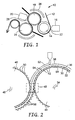
- FIG. 1 illustrates an example casting apparatus 10 for producing a two-sided web 12 that includes registered microreplicated structures on opposing surfaces.
- the casting apparatus 10 includes first and second coating means 16, 20, a nip roller 14, and first and second patterned rolls 18, 24.
- first coating means 16 may be a first extrusion die 16 while second coating means may be a second extrusion die 20.
- the first and second curable liquid is disposed on the web surface prior to passing through the first and second patterned rolls, respectively.
- the first curable liquid is disposed on the first patterned roll and the second curable liquid is disposed on the second patterned roll, which is then transferred to the web from the patterned rolls.
- Web 12 may be presented to the first extrusion die 16, which dispenses a first curable liquid layer coating 22 onto the web 12.
- Nip roller 14 presses first coating 22 into the first patterned roller 18.
- nip roller 14 can be a rubber covered roller.
- energy source 26 may be adapted to provide ultraviolet light.
- ultraviolet light refers to light having a wavelength in a range from 200 to 500 nanometers or from 200 to 400 nanometers.
- a second curable liquid layer 28 is coated on the opposite side of the web 12 using a second side extrusion die 20.
- the second layer 28 is pressed into the second patterned tool roller 24 and the curing process repeated for the second coating layer 28. Registration of the two coating patterns is achieved by maintaining the tool rollers 18, 24 in a precise angular relationship with one another, as will be described hereinafter.
- FIG. 2 provides a closer view at first and second patterned rolls 44 and 46.
- First and second patterned rolls 44, 46 may be considered as particular embodiments of patterned rolls 18, 24 as discussed with respect to FIG.1 . Other patterns are contemplated, as will be discussed in greater detail subsequently.
- First patterned roll 44 has a first pattern 42 for forming a microreplicated surface.
- Second pattern roll 46 has a second microreplicated pattern 50.
- first and second patterns 42, 50 are the same pattern. In other instances, the first and second patterns may be different.
- a first curable liquid (not shown) on a first surface 32 may be cured by curing energy provided by an energy source 34 near a first region 36 on the first patterned roll 44.
- a first microreplicated patterned structure 54 is formed on the first side 43 of the web 30 after the liquid is cured.
- the first patterned structure 54 is a negative of the pattern 42 on the first patterned roll 44.
- a second curable liquid 52 is dispensed onto a second surface 38 of the web 30.
- the second liquid 52 is isolated from the first energy source 34, typically by locating the first energy source 34 so that energy emitted by the first energy source 34 does not fall on the second liquid 52.
- the curing sources can be located inside their respective patterned rolls. As such, the opaque nature of web 30 can aid in preventing undesired curing.
- the web 30 continues along the first roll 44 until it enters a gap region 48 between the first and second patterned rolls 44, 46.
- the second liquid 52 then engages the second pattern 50 on the second patterned roll 46 and is shaped into a second microreplicated structure, which is then cured by curing energy emitted by a second energy source 40.
- the first patterned structured 54 which is by this time substantially cured and bonded to the web 30, restrains the web 30 from slipping while the web 30 begins moving into the gap 48 and around the second patterned roller 46. This removes web stretching and slippages as a source of registration error between the first and second patterned structures formed on the web.
- the degree of registration between the first and second microreplicated structures 54, 56 formed on opposite sides 32, 38 of the web 30 becomes a function of controlling the positional relationship between the surfaces of the first and second patterned rolls 44, 46.
- the S-wrap of the web around the first and second patterned rolls 44, 46 and between the gap 48 formed by the rolls minimizes effects of tension, web strain changes, temperature, microslip caused by mechanics of nipping a web, and lateral position control.
- the S-wrap can maintain the web 30 in contact with each roll over a wrap angle of 180 degrees, though the wrap angle can be more or less depending on the particular requirements.
- microreplicated patterns onto either side of a flexible web or substrate that is opaque, particularly, opaque to curing energy it may be useful to provide microreplicated patterns onto either side of a flexible web or substrate that is transparent, particularly, transparent to curing energy.
- a patterned roll that is transparent to a particular curing energy or includes portions that are transparent to curing energy. In some cases, only one patterned roll is transparent.
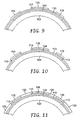
- FIG. 3 is a partial illustration of an illustrative but non-limiting patterned roll and should not be considered as being to scale. Instead, the pattern has been exaggerated for clarity.
- Patterned roll can, as illustrated and as will be discussed in greater detail, may be formed by an additive method in which materials are deposited onto the surface of a transparent cylinder or other suitable shape. In some embodiments, it is believed that patterned roll may be formed using various subtractive methods in which material is removed from a transparent cylinder or other suitable shape.
- Patterned roll includes a transparent cylinder 102 that can be formed of any suitable material.
- transparent cylinder 102 is formed of a material that is transparent to the curing energy that will cure the curable material that will be applied to patterned roll.
- transparent cylinder 102 can be made from a glass such as quartz.
- Quartz cylinder 102 may be of any suitable dimensions, although in some cases quartz cylinder 102 may have a length of 3 inches and a radius of 3 inches. Quartz cylinder 102 may be a substantially solid cylinder, or, as illustrated, quartz cylinder 102 may be a hollow cylinder.
- tie layer 104 it may be useful to apply a thin tie layer 104 to the surface of the quartz cylinder 102. This may assist subsequent materials in adhering or bonding to the quartz. In some instances, tie layer 104 is thin enough to not materially change the optical properties of the quartz cylinder 102. At a minimum, tie layer 104 can be thin enough to remain transparent to curing energy. Tie layer 104 may be formed of any suitable material and using any suitable application technique. In some instances, tie layer 104 includes or consists of titanium and is applied via sputtering.
- tie layer 104 Once tie layer 104 has been formed, subsequent materials may be added to patterned roll. While particular processing steps are illustrated in FIGS. 4-13 , and will be discussed in detail with respect to the Example, a variety of opaque materials may be applied to tie layer 104. Suitable opaque materials include metals such as chrome, copper or aluminum, and curable polymers such as silicone and epoxy. Suitable materials may be applied and patterned using any suitable technique, such as sputtering, etching, and the like.
- the features of patterned roll have been formed in two steps.
- layers 106 have been deposited onto tie layer 104 and subsequently patterned.
- Layers 108 have been formed and patterned on top of layers 106.
- Layers 106 and layers 108 may be formed of different materials or they may be formed of the same material.
- layers 106 may be formed by sputtering a layer of chrome onto tie layer 104.
- layers 108 may be formed by plating chrome onto layers 106.
- the opaque features of patterned roll stand above the surface of quartz cylinder 102.
- the opaque features are actually closer to an outer surface of the substrate, while the transparent features actually penetrate the substrate. In either event, the opaque features may be considered as being farther from a radial center of patterned roll than are the transparent features.
- a patterned roll may be formed from either machinable or non-machinable transparent substrates.
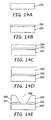
- FIGS. 14-21 Several contemplated manufacturing techniques are described herein in FIGS. 14-21 . It should be noted that in FIGS. 14-21 , only a very small part of a transparent substrate is shown, for ease of illustration. While only a single transparent feature is shown for each potential manufacturing technique, it should be noted that of course a patterned roll will include a number of features. Moreover, it should be noted that a patterned roll will be cylindrical, while for ease of illustration and because only a very small part of the roll is shown, FIGS. 14-21 appear rectangular.
- FIGS. 14A-14E illustrate a potential method of forming opaque features on a non-machinable transparent substrate that includes adding a machinable layer.
- a non-machinable, transparent, substrate 200 is provided.
- non-machinable, transparent substrates include glasses such as quartz.
- a titanium tie layer 202 may be applied to substrate 200 using any suitable technique such as sputtering.
- a copper seed layer 204 may be sputtered onto titanium tie layer 202 as seen in FIG.14C . Additional copper may be plated onto copper seed layer 204 to form copper layer 206, as seen in FIG. 14D .
- FIG. 14E shows that copper layer 206 could be machined in any suitable manner to provide a transparent feature 208 positioned within copper layer 206, which is of course opaque.
- transparent feature 208 could be formed simply by a machining process such as micromilling, laser ablation, diamond turning or EDM processing.
- additional processing such as a brief chemical etch may be useful in exposing transparent substrate 200 without damaging transparent substrate 200.
- machinable layer 206 could be formed from an opaque epoxy or a machinable ceramic that could be coated in a "green” state and sintered after shaping.
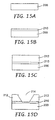
- FIGS. 15A-15D illustrate another potential method of forming opaque features on a non-machinable transparent substrate 200 that includes adding a machinable layer.
- a transparent epoxy layer 210 may be added to the transparent substrate 200 to help protect the transparent substrate during subsequent machining.
- an opaque epoxy layer 212 has been added on top of the transparent epoxy layer 210.
- opaque epoxy layer 212 has been machined using any suitable technique to form transparent feature 214.
- FIGS. 16A-D illustrate another potential method of forming opaque features on a non-machinable transparent substrate 200 that includes adding a machinable layer.
- Transparent substrate 200 is shown in FIG. 16A .
- a relatively thicker transparent epoxy layer 210 has been added atop transparent substrate 200.
- a relatively thinner opaque epoxy layer 212 has been added on transparent epoxy layer 210 as shown in FIG. 16C .
- the opaque epoxy layer 212 and the transparent epoxy layer 210 have been machined using any suitable technique to form transparent feature 216.
- FIGS. 17A-17C illustrate a potential method of forming opaque features on a machinable transparent substrate.
- FIG.17A shows a machinable transparent substrate 220 that can be formed of a machinable transparent polymer. In some instances, substrate 220 can be formed from PMMA (poly methyl methacrylate).
- an opaque coating 222 such as sputtered aluminum or copper has been added onto transparent substrate 220. Alternatively, it is contemplated that opaque coating 222 could also be formed from an opaque epoxy or even an opaque filled epoxy.
- a transparent feature 224 can be formed using any suitable machining technique.
- FIGS. 18A-C illustrate another potential method of forming opaque features on machinable transparent substrate 220.
- transparent substrate 220 has been machined using any suitable technique to form transparent feature 226.
- the portions of transparent substrate 220 beyond transparent feature 226 may be coated with an opaque coating 228.
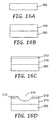
- FIGS.19A-19D illustrate a potential method of using a separately-created master mold to replicate raised features on a transparent substrate. The raised features can then be coated to be opaque.
- a master mold 230 can be cut from any suitable material using standard precision machining techniques. Master mold 230 can be seen to include protrusion 232, which will ultimately form a transparent feature.
- master mold 230 can be filled with an opaque epoxy material 234 and then is applied to the surface of a desired substrate 236 such as quartz or PMMA as seen in FIG. 19C .
- the epoxy can be allowed to cure, and then master mold 230 may be removed, as seen in FIG. 19D , leaving substrate 236 having a transparent feature 238 with an opaque layer 234 on either side of the transparent feature 238.
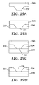
- FIGS. 20A-20E illustrate another potential method of using a separately-created master mold to replicate raised features on a transparent substrate.
- the raised features can then be coated to be opaque.
- a master mold 240 can be cut from any suitable material using standard precision machining techniques. Master mold 240 can be seen to include protrusion 242, which will ultimately form a transparent feature.
- master mold 240 can be filled with a transparent epoxy material 244 and then is applied to the surface of a desired substrate 246 such as quartz or PMMA as seen in FIG. 20C .
- the epoxy can be allowed to cure, and then master mold 240 may be removed, as seen in FIG. 20D , leaving substrate 246 having a transparent feature 248.
- an opaque epoxy layer 250 can be applied to transparent epoxy layer 244 on either side of the transparent feature 248.
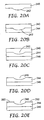
- FIGS. 21A-21D illustrate another potential method of using a separately-created master mold to replicate raised features on a transparent substrate.
- the raised features can then be coated to be opaque.
- a master mold 252 can be cut from any suitable material using standard precision machining techniques. Master mold 252 can be seen to include protrusion 254, which will ultimately form a transparent feature.
- master mold 252 has been imprinted directly into a machinable transparent substrate 256.
- master mold 252 has been removed, leaving transparent substrate 256 including transparent feature 258.
- transparent substrate 256 can be coated with an opaque epoxy layer 258 on either side of transparent feature 258.
- a web 122 is provided to the casting apparatus 120 from a main unwind spool (not shown).
- the exact nature of web 122 can vary widely, depending on the product being produced.
- the casting apparatus 120 is capable of handling a web 122 that is both flexible and transparent and/or opaque, as discussed previously.
- the web 122 is directed around various rollers 126 into the casting apparatus 120.
- Accurate tension control of the web 122 is beneficial in achieving optimal results, so the web 122 may be directed over a tension-sensing device (not illustrated). If an optional liner web is used to protect the web 122, the liner web (not illustrated) can be separated at the unwind spool and directed onto a liner web wind-up spool (not shown).
- the web 122 can be directed via an idler roll to a dancer roller for precision tension control. Idler rollers can direct the web 122 to a position between nip roller 154 and first coating head 156.
- first coating head 156 is a die coating head.
- the web 122 then passes between the nip roll 154 and first patterned roll 160.
- the first patterned roll 160 has a patterned surface 162, and when the web 122 passes between the nip roller 154 and the first patterned roll 160 the material dispensed onto the web 122 by the first coating head 156 is shaped into a negative of patterned surface 162.
- the second coating head 164 is also a die coating arrangement including a second extruder (not shown) and a second coating die (not shown).
- the material dispensed by the first coating head 156 is a composition including a polymer precursor and intended to be cured to solid polymer with the application of curing energy such as ultraviolet radiation.
- the material dispensed by the second coating head 164 is a composition including a polymer precursor and intended to be cured to solid polymer with the application of curing energy such as ultraviolet radiation.
- the web 122 has had a pattern applied to both sides.
- a peel roll 182 may be present to assist in removal of the web 122 from second patterned roll 174.
- the web tension into and out of the casting apparatus is nearly constant.
- the web 122 having a two-sided microreplicated pattern is then directed to a wind-up spool (not shown) via various idler rolls. If an interleave film is desired to protect web 122, it may be provided from a secondary unwind spool (not shown) and the web and interleave film are wound together on the wind-up spool at an appropriate tension.
- first and second patterned rolls are coupled to first and second motor assemblies 210, 220, respectively.
- Support for the motor assemblies 210, 220 is accomplished by mounting assemblies to a frame 230, either directly or indirectly.
- the motor assemblies 210, 220 are coupled to the frame using precision mounting arrangements.
- first motor assembly 210 is fixedly mounted to frame 230.
- Second motor assembly 220 which is placed into position when web 122 is threaded through the casting apparatus 120, may need to be positioned repeatedly and therefore can be movable, both in the cross- and machine direction.
- Movable motor arrangement 220 may be coupled to linear slides 222 to assist in repeated accurate positioning, for example, when switching between patterns on the rolls.
- Second motor arrangement 220 also includes a second mounting arrangement 225 on the backside of the frame 230 for positioning the second patterned roll 174 side-to-side relative to the first patterned roll 160.
- second mounting arrangement 225 includes linear slides 223 allowing accurate positioning in the cross machine directions.
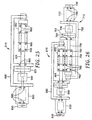
- a motor 633 for driving a tool or patterned roll 662 is mounted to the machine frame 650 and connected through a coupling 640 to a rotating shaft 601 of the patterned roller 662.
- the motor 633 is coupled to a primary encoder 630.
- a secondary encoder 651 is coupled to the tool to provide precise angular registration control of the patterned roll 662.
- Primary 630 and secondary 651 encoders cooperate to provide control of the patterned roll 662 to keep it in registration with a second patterned roll, as will be described further hereinafter.
- Reduction or elimination of shaft resonance is important as this is a source of registration error allowing pattern position control within the specified limits.
- Using a coupling 640 between the motor 633 and shaft 650 that is larger than general sizing schedules specify will also reduce shaft resonance caused by more flexible couplings.
- Bearing assemblies 660 are located in various locations to provide rotational support for the motor arrangement.
- the tool roller 662 diameter can be smaller than its motor 633 diameter.
- tool rollers may be installed in pairs, arranged in mirror image.
- two tool roller assemblies 610, 710 are installed as mirror images in order to be able to bring the two tool rollers 662, 762 together.
- the first motor arrangement is typically fixedly attached to the frame and the second motor arrangement is positioned using movable optical quality linear slides.
- Tool roller assembly 710 is quite similar to tool roller assembly 610, and includes a motor 733 for driving a tool or patterned roll 762 is mounted to the machine frame 750 and connected through a coupling 740 to a rotating shaft 701 of the patterned roller 762.
- the motor 733 is coupled to a primary encoder 730.
- a secondary encoder 751 is coupled to the tool to provide precise angular registration control of the patterned roll 762.
- Primary 730 and secondary 751 encoders cooperate to provide control of the patterned roll 762 to keep it in registration with a second patterned roll, as will be described further hereinafter.
- shaft resonance Reduction or elimination of shaft resonance is important as this is a source of registration error allowing pattern position control within the specified limits.
- Using a coupling 740 between the motor 733 and shaft 750 that is larger than general sizing schedules specify will also reduce shaft resonance caused by more flexible couplings.
- Bearing assemblies 760 are located in various locations to provide rotational support for the motor arrangement.
- each roller must be maintained within a rotational accuracy of ⁇ 32 arc-seconds per revolution. Control of registration becomes more difficult as the speed the web travels through the system is increased.
- Motor arrangement 800 includes a motor 810 including a primary encoder 830 and a drive shaft 820.
- Drive shaft 820 is coupled to a driven shaft 840 of patterned roll 860 through a coupling 825.
- a secondary, or load, encoder 850 is coupled to the driven shaft 840.
- motor arrangement 900 includes a motor 910 including a primary encoder 930 and a drive shaft 920.
- Drive shaft 920 is coupled to a driven shaft 940 of patterned roll 960 through a coupling 930.
- a secondary, or load, encoder 950 is coupled to the driven shaft 940.
- Motor arrangement 900 communicates with a control arrangement 965 to allow precision control of the patterned roll 960.
- Control arrangement 965 includes a drive module 966 and a program module 975.
- the program module 975 communicates with the drive module 966 via a line 977, for example, a SERCOS fiber network.
- the program module 975 is used to input parameters, such as set points, to the drive module 966.
- Drive module 966 receives input 480 volt, 3-phase power 915, rectifies it to DC, and distributes it via a power connection 973 to control the motor 910.
- Motor encoder 912 feeds a position signal to control module 966 via line 972.
- the secondary encoder 950 on the patterned roll 960 also feeds a position signal back to the drive module 966 via to line 971.
- the drive module 966 uses the encoder signals to precisely position the patterned roll 960.
- the control design to achieve the degree of registration is described in detail below.
- each patterned roll is controlled by a dedicated control arrangement.
- Dedicated control arrangements cooperate to control the registration between first and second patterned rolls.
- Each drive module communicates with and controls its respective motor assembly.
- the control arrangement in the system built and demonstrated by Applicants include the following.
- a high performance, low cogging torque motor with a high-resolution sine encoder feedback (512 sine cycles x 4096 drive interpolation » 2 million parts per revolution) was used, model MHD090B-035-NG0-UN, available from Bosch-Rexroth (Indramat).
- model MHD090B-035-NG0-UN available from Bosch-Rexroth (Indramat)
- Bosch-Rexroth Indramat
- model MHD090B-035-NG0-UN available from Bosch-Rexroth (Indramat)
- other types, such as induction motors could also be used.
- Each motor was directly coupled (without gearbox or mechanical reduction) through an extremely stiff bellows coupling, model BK5-300, available from R/W Corporation. Alternate coupling designs could be used, but bellows style generally combines stiffness while providing high rotational accuracy. Each coupling was sized so that a substantially larger coupling was selected than what the typical manufacturers specifications would recommend.
- Each roller shaft was attached to an encoder through a hollow shaft load side encoder, model RON255C, available from Heidenhain Corp., Schaumburg, IL. Encoder selection should have the highest accuracy and resolution possible, typically greater than 32 arc-sec accuracy. Applicants' design, 18000 sine cycles per revolution were employed, which in conjunction with the 4096 bit resolution drive interpolation resulted in excess of 50 million parts per revolution resolution giving a resolution substantially higher than accuracy.
- the load side encoder had an accuracy of +/- 2 arc-sec; maximum deviation in the delivered units was less than +/- 1 arc-sec.
- each shaft may be designed to be as large a diameter as possible and as short as possible to maximize stiffness, resulting in the highest possible resonant frequency. Precision alignment of all rotational components is desired to ensure minimum registration error due to this source of registration error.
- each axis interpolates the position reference with a cubic spline, at the position loop update rate of 250 microsecond intervals.
- the interpolation method is not critical, as the constant velocity results in a simple constant times time interval path.
- the resolution is critical to eliminate any round off or numerical representation errors.
- Axis rollover is also addressed. In some cases, it is important that each axis' control cycle is synchronized at the current loop execution rate (62 microsecond intervals).
- the top path 1151 is the feed forward section of control.
- the control strategy includes a position loop 1110, a velocity loop 1120, and a current loop 1130.
- the position reference 1111 is differentiated, once to generate the velocity feed forward terms 1152 and a second time to generate the acceleration feed forward term 1155.
- the feed forward path 1151 helps performance during line speed changes and dynamic correction.
- the position command 1111 is subtracted from current position 1114, generating an error signal 1116.
- the error 1116 is applied to a proportional controller 1115, generating the velocity command reference 1117.
- the velocity feedback 1167 is subtracted from the command 1117 to generate the velocity error signal 1123, which is then applied to a PID controller.
- the velocity feedback 1167 is generated by differentiating the motor encoder position signal 1126. Due to differentiation and numerical resolution limits, a low pass Butterworth filter 1124 is applied to remove high frequency noise components from the error signal 1123.
- a narrow stop band (notch) filter 1129 is applied at the center of the motor - roller resonant frequency. This allows substantially higher gains to be applied to the velocity controller 1120. Increased resolution of the motor encoder also would improve performance.
- the exact location of the filters in the control diagram is not critical; either the forward or reverse path are acceptable, although tuning parameters are dependent on the location.
- a PID controller could also be used in the position loop, but the additional phase lag of the integrator makes stabilization more difficult.
- the current loop is a traditional PI controller; gains are established by the motor parameters. The highest bandwidth current loop possible will allow optimum performance. Also, minimum torque ripple is desired.
- Minimization of external disturbances is important to obtain maximum registration. This includes motor construction and current loop commutation as previously discussed, but minimizing mechanical disturbances is also important. Examples include extremely smooth tension control in entering and exiting web span, uniform bearing and seal drag, minimizing tension upsets from web peel off from the roller, uniform rubber nip roller.
- a third axis geared to the tool rolls is provided as a pull roll to assist in removing the cured structure from the tool.
- the web material can be any suitable material on which a microreplicated patterned structure can be created. A number of different materials may be used, depending on the ultimate use of the microreplicated patterned structure. If, for example, the microreplicated patterned structure will form a flexible circuit board, the web material may be a metallized polymeric film such as metallized KAPTON.
- the liquid from which the microreplicated structures are created can be a curable photocurable material, such as acrylates curable by UV light.
- a curable photocurable material such as acrylates curable by UV light.
- other coating materials can be used, for example, polymerizable material, and selection of a material will depend on the particular characteristics desired for the microreplicated structures.
- the coating material may include a conductive or insulating polymer.
- the coating material includes an electroplate masking material and/or nonconductive or insulating polymers.
- coating means that useful for delivering and controlling liquid to the web or patterned roll are, for example, die or knife coating, coupled with any suitable pump such as a syringe or peristaltic pump.
- any suitable pump such as a syringe or peristaltic pump.
- coating means can be used, and selection of a particular means will depend on the particular characteristics of the liquid to be delivered to the web or patterned roll.
- curing energy sources are infrared radiation, ultraviolet radiation, visible light radiation, or microwave.
- curing sources can be used, and selection of a particular web material/curing source combination will depend on the particular article (having microreplicated structures in registration) to be created.
- FIG. 30 schematically illustrates a contemplated coated microreplicated article 1200 formed according to the methods and using the apparatus described herein.
- Article 1200 includes a flexible opaque web 1202 and a number of schematic elements disposed on either side of opaque web 1202.
- Element 1204 is disposed opposite element 1206.
- element 1208, element 1212 and element 1216 are disposed opposite element 1210, element 1214 and element 1218, respectively.
- these elements can be considered as generically representing a number of different potential elements. These elements may be circuitry, for example.
- the microreplicated pattern includes an electroplate mask that can pass through an additive circuit plating step.
- the coated material is an electrically conductive material or an electroplate mask.
- an additional washing step can remove uncured material from the microreplicated pattern to produce a microreplicated features having no land areas and separated from one another.
- article 1202 may include lands, i.e. coated material remaining on opaque web 1202 between adjacent elements.
- FIGS. 4-13 illustrate an additive process for forming a patterned roll much like patterned roll of FIG. 3 .
- Quartz tubes 3 inches long and 3 inches in radius were cleaned with water, acetone and methyl ethyl ketone (MEK), and were then placed under a UV lamp for 15 minutes.
- the quartz tubes were then mounted on a rotating table in a high vacuum sputter chamber, and the pressure within the chamber was slowly reduced to 1 x 10 -6 Torr over a period of one hour.
- a strip of chrome plated steel previously mounted within the chamber was electrically connected to an arc welder. The arc welder passed a current through the metal strip and the metal strip was thus heated to red hot.
- the rotating quartz tubes were washed by the resulting IR radiation for 10 minutes.
- a quartz cylinder 102 as seen in FIG. 4 was sputtered with a thin layer 104 of chrome, which acts as an adhesion layer between the quartz and the nickel layer to follow.
- a nickel metallization layer 110 was sputtered onto the chrome tie layer 104.
- a protective copper layer 112 was applied over the nickel metallization layer 110.
- the copper layer 112 was a sacrificial layer that was intended to protect the nickel layer 110 from contamination and oxidation during subsequent processing steps.
- a photoresist (SC Resists, Arch Semiconductor Photopolymers Company) layer 114 has been added on top of the copper layer 112.
- the height of the photoresist layer 114 ultimately sets the height of the features being formed on quartz cylinder 102.
- the photoresist layer 114 was formed to be 50 micrometers thick, and was softbaked at 115 degrees Celsius for 30 seconds prior to exposure.
- the photoresist layer 114 was patterned by shining light in a desired pattern onto the photoresist layer 114. Consequently, the photoresist layer 114 now has portions 116 that will remain, and portions 118 that will be removed after developing.
- the photoresist was developed. After sitting for at least 30 minutes, the photoresist was subjected to a post exposure bake at 115 degrees Celsius for 1 minute. The photoresist was then developed via exposure to developing solution for 30 to 60 seconds. Consequently, resist portions 116 remain on copper layer 112 while resist portions 118 have been removed.
- the exposed portions of copper layer 112 were removed in an etching process.
- Sodium persulfate was used to remove the exposed copper because sodium persulfate reacts quickly with copper but slowly with the chrome underlying the copper, as it is desirable to keep the chrome layer as thick as possible.
- chrome sections 120 were plated onto the freshly exposed chrome layer 110, in between resist regions 116.
- Chrome sections 120 were plated using low current densities on the order of 1mA/17mm 2 . As the current density increases, even at levels as low as 20mA/17mm 2 , either internal stress was high, causing the chrome to peel off, or severe pitting occurred.
- the geometry of chrome sections 120 were determined by resist regions 116.
- the remaining cured photoresist, in resist regions 116 were removed using a basic solution.
- the remaining copper layer 112 was removed using a sodium persulfate bath as discussed above.
- the resulting patterned roll has opaque regions corresponding to nickel 110 and chrome sections 120, and transparent regions corresponding to where tie layer 104 is not covered by opaque material.
Claims (5)
- Rouleau structuré (18, 44; 24, 46), comprenant:un cylindre transparent à l'énergie de durcissement (102) qui présente une surface extérieure, le cylindre transparent à l'énergie de durcissement (102) permettant à au moins 10 pour cent de la lumière de durcissement incidente sur le cylindre de passer à travers le cylindre;une couche de liaison (104) qui est disposée sur la surface extérieure du cylindre transparent à l'énergie de durcissement (102); etune pluralité de caractéristiques opaques à l'énergie de durcissement (106, 108; 110, 120) disposée sur la couche de liaison (104) pour former un motif, les caractéristiques opaques à l'énergie de durcissement bloquant au moins 95 pour cent de la lumière de durcissement incidente sur les caractéristiques opaques à l'énergie de durcissement (106, 108; 110, 120).
- Rouleau structuré selon la revendication 1, dans lequel le cylindre transparent à l'énergie de durcissement (102) comprend un cylindre de quartz.
- Rouleau structuré selon la revendication 1, dans lequel la couche de liaison (104) comprend une couche de liaison en titane.
- Rouleau structuré selon la revendication 1, dans lequel la pluralité de caractéristiques opaques à l'énergie de durcissement (106, 108; 110, 120) comprend une pluralité de caractéristiques de chrome.
- Rouleau structuré selon la revendication 1, dans lequel au moins plusieurs caractéristiques opaques à l'énergie de durcissement sélectionnées sont entourées par une surface de substrat transparente à l'énergie de durcissement.
Applications Claiming Priority (2)
| Application Number | Priority Date | Filing Date | Title |
|---|---|---|---|
| US66143005P | 2005-03-09 | 2005-03-09 | |
| EP06737180A EP1871584B1 (fr) | 2005-03-09 | 2006-03-06 | Appareil et procede de production de bande a motif a deux cotes coincidants |
Related Parent Applications (2)
| Application Number | Title | Priority Date | Filing Date |
|---|---|---|---|
| EP06737180A Division EP1871584B1 (fr) | 2005-03-09 | 2006-03-06 | Appareil et procede de production de bande a motif a deux cotes coincidants |
| EP06737180.7 Division | 2006-03-06 |
Publications (3)
| Publication Number | Publication Date |
|---|---|
| EP2058108A2 EP2058108A2 (fr) | 2009-05-13 |
| EP2058108A3 EP2058108A3 (fr) | 2009-12-09 |
| EP2058108B1 true EP2058108B1 (fr) | 2012-06-06 |
Family
ID=36602594
Family Applications (2)
| Application Number | Title | Priority Date | Filing Date |
|---|---|---|---|
| EP06737180A Not-in-force EP1871584B1 (fr) | 2005-03-09 | 2006-03-06 | Appareil et procede de production de bande a motif a deux cotes coincidants |
| EP09001026A Not-in-force EP2058108B1 (fr) | 2005-03-09 | 2006-03-06 | Rouleau structuré pour moulage d'une surface structurée sur une bande opaque |
Family Applications Before (1)
| Application Number | Title | Priority Date | Filing Date |
|---|---|---|---|
| EP06737180A Not-in-force EP1871584B1 (fr) | 2005-03-09 | 2006-03-06 | Appareil et procede de production de bande a motif a deux cotes coincidants |
Country Status (10)
| Country | Link |
|---|---|
| US (3) | US7767273B2 (fr) |
| EP (2) | EP1871584B1 (fr) |
| JP (1) | JP4861400B2 (fr) |
| KR (1) | KR101300866B1 (fr) |
| CN (1) | CN101137481A (fr) |
| AT (1) | ATE448927T1 (fr) |
| BR (1) | BRPI0608406A2 (fr) |
| DE (1) | DE602006010529D1 (fr) |
| MX (1) | MX2007010858A (fr) |
| WO (1) | WO2006098935A1 (fr) |
Families Citing this family (36)
| Publication number | Priority date | Publication date | Assignee | Title |
|---|---|---|---|---|
| US20050231809A1 (en) * | 2003-09-09 | 2005-10-20 | Carlson Daniel H | Microreplicated polarizing article |
| US7804649B2 (en) * | 2003-09-09 | 2010-09-28 | 3M Innovative Properties Company | Microreplicated achromatic lens |
| US7224529B2 (en) * | 2003-09-09 | 2007-05-29 | 3M Innovative Properties Company | Microreplicated article |
| US7165959B2 (en) * | 2003-09-09 | 2007-01-23 | 3M Innovative Properties Company | Apparatus and method for producing two-sided patterned webs in registration |
| BRPI0609284A2 (pt) * | 2005-03-09 | 2010-09-08 | 3M Innovative Properties Co | artigo microrreplicado, método de produzir um artigo microrreplicado, e, monitor óptico |
| US7767273B2 (en) * | 2005-03-09 | 2010-08-03 | 3M Innovative Properties Company | Apparatus and method for producing two-sided patterned web in registration |
| WO2006098958A1 (fr) * | 2005-03-09 | 2006-09-21 | 3M Innovative Properties Company | Article micro-duplique avec une surface reduisant les defauts |
| CN101137449B (zh) | 2005-03-09 | 2012-08-29 | 3M创新有限公司 | 微复制物品及其生产方法 |
| EP1874524B1 (fr) * | 2005-03-09 | 2009-03-11 | 3M Innovative Properties Company | Appareil et procede de fabrication d'un article microreproduit |
| US7906057B2 (en) * | 2005-07-14 | 2011-03-15 | 3M Innovative Properties Company | Nanostructured article and method of making the same |
| EP2084005B1 (fr) * | 2006-11-21 | 2012-06-13 | Basf Se | Appareil et procédé pour fabriquer un produit de sécurité |
| WO2008088650A1 (fr) * | 2007-01-11 | 2008-07-24 | 3M Innovative Properties Company | Détecteur de position longitudinale de nappe |
| JP2010532466A (ja) * | 2007-06-19 | 2010-10-07 | スリーエム イノベイティブ プロパティズ カンパニー | ウェブの位置を表示するためのシステム及び方法 |
| EP2165162A2 (fr) * | 2007-06-19 | 2010-03-24 | 3M Innovative Properties Company | Échelle de déplacement de réflexion interne totale |
| EP2162705A4 (fr) * | 2007-06-19 | 2014-02-19 | 3M Innovative Properties Co | Systèmes et procédés pour fabriquer des échelles de déplacement |
| AU2009238168B2 (en) * | 2008-04-16 | 2014-02-20 | Vale Inco Limited | Process for production of nickel and cobalt using metal hydroxide, metal oxide and/or metal carbonate |
| SG172349A1 (en) | 2008-12-29 | 2011-07-28 | 3M Innovative Properties Co | Phase-locked web position signal using web fiducials |
| CN102272375B (zh) | 2008-12-30 | 2014-01-08 | 3M创新有限公司 | 用于在基底上形成基准的设备和方法 |
| KR101433292B1 (ko) * | 2009-02-17 | 2014-08-22 | 더 보드 오브 트러스티즈 오브 더 유니버시티 오브 일리노이 | 마이크로구조 제조방법 |
| KR101590102B1 (ko) * | 2009-05-07 | 2016-01-29 | 삼성전자 주식회사 | 롤투롤 패터닝 장치 및 이를 갖춘 패터닝 시스템 |
| US8339573B2 (en) * | 2009-05-27 | 2012-12-25 | 3M Innovative Properties Company | Method and apparatus for photoimaging a substrate |
| KR100988935B1 (ko) | 2009-10-28 | 2010-10-20 | 한국기계연구원 | 롤 임프린트 장치 |
| US10265719B2 (en) | 2011-04-13 | 2019-04-23 | Durr Megtec, Llc | Method and apparatus for coating discrete patches |
| KR20140035454A (ko) | 2011-05-31 | 2014-03-21 | 쓰리엠 이노베이티브 프로퍼티즈 캄파니 | 불연속 형상을 갖는 미세구조화 공구의 제조 방법, 및 그로부터 제조된 용품 |
| JP5973561B2 (ja) * | 2011-05-31 | 2016-08-23 | スリーエム イノベイティブ プロパティズ カンパニー | 相異するようにパターン硬化された微細構造化物品を作製する方法 |
| KR101913600B1 (ko) | 2011-06-03 | 2018-10-31 | 바브콕 앤드 윌콕스 메그텍, 엘엘시 | 웹 리프터/스태빌라이저 및 방법 |
| WO2013062755A1 (fr) * | 2011-10-24 | 2013-05-02 | Rolith, Inc. | Lithographie à pas de détails réduit utilisant des techniques avec masque rotatif |
| JP6105214B2 (ja) * | 2012-06-07 | 2017-03-29 | 旭化成株式会社 | 微細凹凸構造を表面に有する基材の製造方法 |
| KR20140141815A (ko) * | 2013-05-31 | 2014-12-11 | 삼성전자주식회사 | 전자기기용 케이스 및 이의 표면 처리방법 |
| WO2015144174A1 (fr) * | 2014-03-24 | 2015-10-01 | Inmold A/S | Procédé et appareil de production d'une feuille nanostructurée à rapport d'aspect élevé par revêtement par extrusion ou moulage par extrusion |
| JP6076946B2 (ja) * | 2014-08-04 | 2017-02-08 | 大日本印刷株式会社 | ローラーインプリント用モールドとインプリント方法およびワイヤーグリッド偏光子とその製造方法 |
| US20160231054A1 (en) * | 2015-02-05 | 2016-08-11 | Air Motion Systems, Inc. | Apparatus for curing sensitive substrate materials |
| CN104703408B (zh) * | 2015-03-10 | 2018-05-15 | 上海量子绘景电子股份有限公司 | 高密度覆铜线路板的制备方法 |
| JP6550291B2 (ja) * | 2015-07-29 | 2019-07-24 | 東芝機械株式会社 | フィルムのパターン転写装置およびフィルムのパターン転写方法 |
| US10253502B2 (en) * | 2016-08-29 | 2019-04-09 | Polyglass S.P.A. | Apparatus and process to create 3-D pattern on material |
| KR102341780B1 (ko) | 2017-05-25 | 2021-12-20 | 매직 립, 인코포레이티드 | 양면 임프린팅 |
Citations (1)
| Publication number | Priority date | Publication date | Assignee | Title |
|---|---|---|---|---|
| US5540147A (en) * | 1994-12-02 | 1996-07-30 | Corning Incorporated | Method for forming a contoured planarizing layer for a color filter |
Family Cites Families (125)
| Publication number | Priority date | Publication date | Assignee | Title |
|---|---|---|---|---|
| US3241429A (en) | 1962-05-14 | 1966-03-22 | Pid Corp | Pictorial parallax panoramagram units |
| US3374303A (en) | 1964-02-14 | 1968-03-19 | Crown Zellerbach Corp | Method for manufacturing imprinted plastic film |
| US3551544A (en) | 1965-12-06 | 1970-12-29 | Tenex Corp | Method of continuously forming an elongated cleated runner of plastic material |
| US3893795A (en) | 1970-08-20 | 1975-07-08 | Rowland Dev Corp | Embossing rolls with areas of differential hardness |
| US3917772A (en) | 1972-02-10 | 1975-11-04 | Grace W R & Co | Method for producing battery separator sheet |
| DE2632107C2 (de) | 1975-07-16 | 1986-01-09 | Ludwig Dr. Vacallo Tessin Eigenmann | Rückstrahlaggregat für Markierungsmaterial zur horizontalen Straßenmarkierung |
| JPS5351253Y2 (fr) | 1976-02-05 | 1978-12-07 | ||
| US4078416A (en) * | 1976-10-07 | 1978-03-14 | The Minster Machine Company | Method and apparatus for feeding strip stock into a machine |
| JPS5917656B2 (ja) * | 1976-10-21 | 1984-04-23 | 東洋インキ製造株式会社 | 模様形成法 |
| US4177304A (en) | 1977-03-17 | 1979-12-04 | Beloit Corporation | Method of coating both sides of a travelling web |
| US6630970B2 (en) | 2001-07-02 | 2003-10-07 | 3M Innovative Properties Company | Polarizers for use with liquid crystal displays |
| US4249878A (en) | 1979-05-10 | 1981-02-10 | K. R. Komarek, Inc. | Briquetting press |
| US4280978A (en) | 1979-05-23 | 1981-07-28 | Monsanto Company | Process of embossing and perforating thermoplastic film |
| US4420502A (en) | 1980-09-05 | 1983-12-13 | Conley Kenneth E | Apparatus and method for producing a flexible sheet material having a predetermined surface characteristic |
| US4414316A (en) | 1980-09-05 | 1983-11-08 | Rexham Corporation | Composite lenticular screen sheet |
| DE3206164C2 (de) | 1981-03-16 | 1985-02-21 | Heinz Georg Hünibach Thun Baus | Vorrichtung zur Herstellung von Mehrschicht-Platten |
| DE3279203D1 (en) | 1981-03-16 | 1988-12-15 | Heinz Georg Baus | Method for producing multi-layered plates |
| EP0158085B1 (fr) | 1984-03-08 | 1989-01-18 | Altura Leiden Holding B.V. | Appareil pour fabriquer des plaques ainsi que plaques fabriquées au moyen de l'appareil |
| US4744936A (en) | 1986-01-30 | 1988-05-17 | Plastic Film Corporation Of America | Process for embossing thermoplastic material |
| DE3609090A1 (de) | 1986-03-18 | 1987-09-24 | Gao Ges Automation Org | Wertpapier mit darin eingelagertem sicherheitsfaden und verfahren zur herstellung derselben |
| US4836874A (en) | 1987-01-30 | 1989-06-06 | Foster Michael S | Method of mass producing damage-resistant compact discs |
| US5164227A (en) | 1987-06-19 | 1992-11-17 | Van Leer Metallized Products (Usa) Limited | Method for embossing a coated sheet with a diffraction or holographic pattern |
| US5028361A (en) | 1987-11-09 | 1991-07-02 | Takeo Fujimoto | Method for molding a photosensitive composition |
| EP0405898A3 (en) * | 1989-06-26 | 1991-02-06 | Canon Kabushiki Kaisha | Apparatus for producing substrate sheet for optical recording mediums, and process for producing substrate sheet therefor making use of it |
| DE4001105C1 (fr) | 1990-01-17 | 1991-08-08 | Hermann Berstorff Maschinenbau Gmbh, 3000 Hannover, De | |
| US6724536B2 (en) | 1990-05-18 | 2004-04-20 | University Of Arkansas | Directional image lenticular window sheet |
| US5177637A (en) | 1990-09-11 | 1993-01-05 | Nikon Corporation | Focusing screen including different height microlenses arranged in a cyclical pattern |
| JP2883436B2 (ja) * | 1990-10-18 | 1999-04-19 | 大日本印刷株式会社 | ホログラムの複製方法及び装置 |
| JP3158476B2 (ja) | 1991-03-28 | 2001-04-23 | 凸版印刷株式会社 | 両面レンチキュラーシートの製造方法 |
| JPH0580530A (ja) * | 1991-09-24 | 1993-04-02 | Hitachi Ltd | 薄膜パターン製造方法 |
| US5409772A (en) | 1991-09-27 | 1995-04-25 | Toppan Printing Co., Ltd. | Composite laminate |
| DE4132476A1 (de) | 1991-09-30 | 1993-04-01 | Matthiesen Geb Sievers Gerda | Verfahren, bedruckstoff und einrichtung zur verfielfaeltigung von holographischen feinstrukturen und anderen beugungsgittern auf printprodukte |
| WO1993023244A1 (fr) | 1992-05-08 | 1993-11-25 | Raymond Enterprises, Inc. | Systeme optique lenticulaire |
| JP2756211B2 (ja) | 1992-06-17 | 1998-05-25 | ワイケイケイ株式会社 | 両面に係合片を有する一体成形面ファスナーの製造方法及びその装置 |
| US5301981A (en) | 1992-07-09 | 1994-04-12 | Docusafe, Ltd. | Copy preventing device and method |
| DE4226906A1 (de) | 1992-08-14 | 1994-02-17 | Basf Magnetics Gmbh | Anti-Kopier-Film oder -Schicht für Dokumente |
| US5330799A (en) | 1992-09-15 | 1994-07-19 | The Phscologram Venture, Inc. | Press polymerization of lenticular images |
| US5448401A (en) | 1992-12-25 | 1995-09-05 | Sony Corporation | Screen of projection display |
| KR0168879B1 (ko) | 1992-12-25 | 1999-04-15 | 기따지마 요시또시 | 렌티큘러 렌즈, 면광원 및 액정 표시 장치 |
| US5333072A (en) | 1992-12-31 | 1994-07-26 | Minnesota Mining And Manufacturing Company | Reflective liquid crystal display overhead projection system using a reflective linear polarizer and a fresnel lens |
| DE69405451T2 (de) | 1993-03-16 | 1998-03-12 | Koninkl Philips Electronics Nv | Verfahren und Vorrichtung zur Herstellung eines strukturierten Reliefbildes aus vernetztem Photoresist auf einer flachen Substratoberfläche |
| EP0623440B1 (fr) | 1993-03-16 | 1997-09-10 | Koninklijke Philips Electronics N.V. | Procédé de et dispositif pour l'obtention d'un motif structuré avec une photoréserve réticulée sur la surface d'un substrat plat |
| US5598280A (en) | 1993-03-23 | 1997-01-28 | Dai Nippon Printing Co., Ltd. | Film lens and a surface light source using the same |
| US5691846A (en) | 1993-10-20 | 1997-11-25 | Minnesota Mining And Manufacturing Company | Ultra-flexible retroreflective cube corner composite sheetings and methods of manufacture |
| US5579164A (en) | 1993-11-12 | 1996-11-26 | Pharos Technology Corporation | Spatially multiplexed image display system |
| JP3230915B2 (ja) | 1993-11-29 | 2001-11-19 | 三菱レイヨン株式会社 | 両面レンズシートの製造方法 |
| JPH07175131A (ja) | 1993-12-20 | 1995-07-14 | Mitsubishi Rayon Co Ltd | レンズシートおよびその製造方法 |
| US6025897A (en) | 1993-12-21 | 2000-02-15 | 3M Innovative Properties Co. | Display with reflective polarizer and randomizing cavity |
| US5759455A (en) | 1994-07-08 | 1998-06-02 | Canon Kabushiki Kaisha | Roller-shaped stamper for fabricating optical scales |
| EP0871923A1 (fr) | 1995-06-26 | 1998-10-21 | Minnesota Mining And Manufacturing Company | Dispositifs transflectifs a transflecteur de polarisation reflechissant |
| US6130777A (en) | 1996-05-16 | 2000-10-10 | Dai Nippon Printing Co., Ltd. | Lenticular lens sheet with both a base sheet having lenticular elements and a surface diffusing part having elements of elementary shape smaller than lenticular elements |
| US5914760A (en) | 1996-06-21 | 1999-06-22 | Casio Computer Co., Ltd. | Surface light source device and liquid crystal display device using the same |
| US5800723A (en) | 1996-12-10 | 1998-09-01 | Motorola, Inc. | Process for fabricating flex circuits and product thereby |
| US6197397B1 (en) | 1996-12-31 | 2001-03-06 | 3M Innovative Properties Company | Adhesives having a microreplicated topography and methods of making and using same |
| US6261938B1 (en) * | 1997-02-12 | 2001-07-17 | Quantiscript, Inc. | Fabrication of sub-micron etch-resistant metal/semiconductor structures using resistless electron beam lithography |
| US5922238A (en) | 1997-02-14 | 1999-07-13 | Physical Optics Corporation | Method of making replicas and compositions for use therewith |
| US6280063B1 (en) | 1997-05-09 | 2001-08-28 | 3M Innovative Properties Company | Brightness enhancement article |
| DE19721170A1 (de) | 1997-05-21 | 1998-11-26 | Emtec Magnetics Gmbh | Verfahren und Vorrichtung zum Herstellen eines Films oder einer Schicht mit beidseitiger Oberflächenstruktur |
| US6577358B1 (en) | 1997-06-25 | 2003-06-10 | Dai Nippon Printing Co., Ltd. | Lens film with conductive lens layer or conductive layer |
| KR100485218B1 (ko) | 1997-06-30 | 2005-08-10 | 주식회사 엘지화학 | 투사형텔레비젼스크린 |
| CA2244324A1 (fr) * | 1997-08-04 | 1999-02-04 | Hsm Holographic Systems Munchen Gmbh | Methode et appareil de fabrication d'une structure de surface sur un substrat, particulierement une surface holographique |
| US6074192A (en) | 1997-09-11 | 2000-06-13 | Mikkelsen; Oeystein | Lenticular pattern forming roll and method for making the roll |
| JP2001517329A (ja) | 1997-12-16 | 2001-10-02 | ゴスダルストベンニ ナウチニ ツェントル ロシイスコイ フェデラツィイ“ニオピク”(ゲーエヌテーエス エルエフ“ニオピク”) | 偏光子及び液晶表示素子 |
| US6024455A (en) | 1998-01-13 | 2000-02-15 | 3M Innovative Properties Company | Reflective article with concealed retroreflective pattern |
| CA2282853C (fr) | 1998-01-30 | 2002-01-01 | James H. Stauffacher | Dispositif et procede d'impression et d'estampage de substrats allonges |
| DE69939647D1 (de) | 1998-02-18 | 2008-11-13 | Minnesota Mining & Mfg | Optischer film |
| KR100604123B1 (ko) | 1998-08-05 | 2006-07-25 | 미쯔비시 레이온 가부시끼가이샤 | 렌즈 시트 및 그 제조방법 |
| US6149849A (en) | 1998-08-14 | 2000-11-21 | The Procter & Gamble Copmany | Process and apparatus for making papermaking belt |
| US6187250B1 (en) | 1998-08-19 | 2001-02-13 | James Champagne | Continuous gel casting method and apparatus |
| US6266476B1 (en) | 1998-08-25 | 2001-07-24 | Physical Optics Corporation | Optical element having an integral surface diffuser |
| JP3542329B2 (ja) | 1998-09-16 | 2004-07-14 | 富士通株式会社 | 光学装置およびこれを用いた表示装置 |
| JP2000121932A (ja) * | 1998-10-20 | 2000-04-28 | Minolta Co Ltd | 撮影光学系及び縮小光学系 |
| JP2000183253A (ja) * | 1998-12-14 | 2000-06-30 | Kyocera Corp | 半導体素子収納用パッケージ |
| US6411362B2 (en) * | 1999-01-04 | 2002-06-25 | International Business Machines Corporation | Rotational mask scanning exposure method and apparatus |
| US6272275B1 (en) | 1999-06-25 | 2001-08-07 | Corning Incorporated | Print-molding for process for planar waveguides |
| EP1141766A1 (fr) | 1999-09-30 | 2001-10-10 | Koninklijke Philips Electronics N.V. | Dispositif lenticulaire |
| US6845212B2 (en) | 1999-10-08 | 2005-01-18 | 3M Innovative Properties Company | Optical element having programmed optical structures |
| KR100647938B1 (ko) | 1999-10-08 | 2006-11-17 | 스미토모 베이클리트 컴퍼니 리미티드 | 고분자 시트의 제조방법 및 광학 고분자 시트 |
| US6368682B1 (en) | 1999-10-22 | 2002-04-09 | 3M Innovative Properties Company | Composition and structures made therefrom |
| US6908295B2 (en) | 2000-06-16 | 2005-06-21 | Avery Dennison Corporation | Process and apparatus for embossing precise microstructures and embossing tool for making same |
| CA2413700C (fr) | 2000-07-11 | 2007-01-09 | 3M Innovative Properties Company | Retroeclairage a surfaces structurees |
| US6373636B1 (en) | 2000-09-08 | 2002-04-16 | Kenneth E. Conley | Heat stabilized and dimensionally stable thin lenticular film |
| JP2002090889A (ja) | 2000-09-14 | 2002-03-27 | Kuraray Co Ltd | 背面投射型スクリーン及びその製造方法 |
| JP2002113728A (ja) * | 2000-10-06 | 2002-04-16 | Mitsubishi Rayon Co Ltd | レンズシートの製造方法 |
| US6541774B1 (en) * | 2000-11-03 | 2003-04-01 | General Electric Company | Radiation imager cover |
| JP2002210915A (ja) | 2001-01-22 | 2002-07-31 | Tokyo Kikai Seisakusho Ltd | 分割版胴を個別に駆動する多色刷平版印刷機 |
| WO2002063392A1 (fr) * | 2001-02-07 | 2002-08-15 | Corning Incorporated | Masques a ouvertures auto-alignes pourvus d'ouvertures de haute definition |
| ITPS20010006A1 (it) | 2001-02-23 | 2002-08-23 | Canti & Figli Srl | Procedimento e macchina atti ad ottenere goffrature su superfici verniciate di pannelli o di pellicole di rivestimento ed elementi ottenuti |
| JP2002287256A (ja) | 2001-03-27 | 2002-10-03 | Mitsubishi Rayon Co Ltd | 両面レンチキュラーレンズシート |
| EP1248160B8 (fr) | 2001-04-03 | 2009-11-04 | Sharp Kabushiki Kaisha | Dispositif de développement, procédé pour charger utilisé pour ceci, et appareil d'impression avec le dispositif de développement |
| DE60228943D1 (de) | 2001-04-10 | 2008-10-30 | Harvard College | Mikrolinse zur projektionslithographie und ihr herstellungsverfahren |
| US6814901B2 (en) | 2001-04-20 | 2004-11-09 | Matsushita Electric Industrial Co., Ltd. | Method of manufacturing microlens array and microlens array |
| US7420005B2 (en) | 2001-06-28 | 2008-09-02 | Dai Nippon Printing Co., Ltd. | Photocurable resin composition, finely embossed pattern-forming sheet, finely embossed transfer sheet, optical article, stamper and method of forming finely embossed pattern |
| JP4153686B2 (ja) | 2001-09-26 | 2008-09-24 | 大日本スクリーン製造株式会社 | 成膜液乾燥装置 |
| US6863107B2 (en) | 2001-10-02 | 2005-03-08 | Sca Hygiene Products Gmbh | Device for applying a spot embossing pattern to a web of multi-ply tissue paper |
| WO2003042413A1 (fr) * | 2001-10-23 | 2003-05-22 | Steen Research, Llc | Procede et compositions permettant de traiter des plumes de volaille |
| US6717749B2 (en) | 2001-11-01 | 2004-04-06 | Pentax Corporation | Cemented lens group |
| US20030108710A1 (en) | 2001-12-07 | 2003-06-12 | General Electric Company | Articles bearing patterned microstructures and method of making |
| WO2003078152A1 (fr) | 2002-03-15 | 2003-09-25 | The Procter & Gamble Company | Elements destines a des applications de gaufrage et d'adhesion |
| AT502319B1 (de) | 2002-04-11 | 2009-11-15 | Hueck Folien Gmbh | Substrate mit vorzugsweise transferierbaren schichten und/oder oberflächenstrukturen, verfahren zu deren herstellung und deren verwendung |
| US7140812B2 (en) | 2002-05-29 | 2006-11-28 | 3M Innovative Properties Company | Diamond tool with a multi-tipped diamond |
| DE10242441A1 (de) | 2002-09-11 | 2004-04-01 | Erco Leuchten Gmbh | Leuchte |
| CN100376924C (zh) | 2002-09-19 | 2008-03-26 | 三菱电机株式会社 | 显示装置和具有该显示装置的电子设备 |
| US6963184B2 (en) | 2002-09-26 | 2005-11-08 | 3M Innovative Properties Company | Adaptable spatial notch filter |
| US7186004B2 (en) | 2002-12-31 | 2007-03-06 | Karlton David Powell | Homogenizing optical sheet, method of manufacture, and illumination system |
| US7070406B2 (en) | 2003-04-29 | 2006-07-04 | Hewlett-Packard Development Company, L.P. | Apparatus for embossing a flexible substrate with a pattern carried by an optically transparent compliant media |
| WO2004099823A2 (fr) | 2003-05-02 | 2004-11-18 | Reflexite Corporation | Structures optiques de reorientation de lumiere |
| WO2004103683A1 (fr) | 2003-05-23 | 2004-12-02 | Dai Nippon Printing Co., Ltd. | Procede de production d'une feuille optique et feuille optique |
| JP4376128B2 (ja) | 2003-05-23 | 2009-12-02 | 大日本印刷株式会社 | 光学シート及びその製造方法 |
| US20050008821A1 (en) | 2003-07-07 | 2005-01-13 | Pricone Robert M. | Process and apparatus for fabricating precise microstructures and polymeric molds for making same |
| JP2005053004A (ja) * | 2003-08-06 | 2005-03-03 | Meiwa Gravure Co Ltd | 高輝度成型品とその製造方法 |
| US7804649B2 (en) | 2003-09-09 | 2010-09-28 | 3M Innovative Properties Company | Microreplicated achromatic lens |
| US7224529B2 (en) | 2003-09-09 | 2007-05-29 | 3M Innovative Properties Company | Microreplicated article |
| US7165959B2 (en) | 2003-09-09 | 2007-01-23 | 3M Innovative Properties Company | Apparatus and method for producing two-sided patterned webs in registration |
| US20050231809A1 (en) | 2003-09-09 | 2005-10-20 | Carlson Daniel H | Microreplicated polarizing article |
| US7106517B2 (en) | 2003-12-31 | 2006-09-12 | General Electric Company | Display optical films |
| US7808706B2 (en) | 2004-02-12 | 2010-10-05 | Tredegar Newco, Inc. | Light management films for displays |
| US20050224997A1 (en) | 2004-04-08 | 2005-10-13 | Tsung-Neng Liao | Method of fabricating optical substrate |
| WO2006098958A1 (fr) | 2005-03-09 | 2006-09-21 | 3M Innovative Properties Company | Article micro-duplique avec une surface reduisant les defauts |
| EP1874524B1 (fr) | 2005-03-09 | 2009-03-11 | 3M Innovative Properties Company | Appareil et procede de fabrication d'un article microreproduit |
| BRPI0609284A2 (pt) | 2005-03-09 | 2010-09-08 | 3M Innovative Properties Co | artigo microrreplicado, método de produzir um artigo microrreplicado, e, monitor óptico |
| CN101137449B (zh) | 2005-03-09 | 2012-08-29 | 3M创新有限公司 | 微复制物品及其生产方法 |
| WO2006098934A1 (fr) | 2005-03-09 | 2006-09-21 | 3M Innovative Properties Company | Appareil et procede de fabrication d'articles microrepliques |
| US7767273B2 (en) | 2005-03-09 | 2010-08-03 | 3M Innovative Properties Company | Apparatus and method for producing two-sided patterned web in registration |
| US20080210714A1 (en) * | 2007-03-01 | 2008-09-04 | Atlantic Industries | Bulk tea dispensing system |
-
2006
- 2006-03-06 US US11/370,136 patent/US7767273B2/en not_active Expired - Fee Related
- 2006-03-06 MX MX2007010858A patent/MX2007010858A/es not_active Application Discontinuation
- 2006-03-06 AT AT06737180T patent/ATE448927T1/de not_active IP Right Cessation
- 2006-03-06 WO PCT/US2006/007972 patent/WO2006098935A1/fr active Application Filing
- 2006-03-06 BR BRPI0608406-0A patent/BRPI0608406A2/pt not_active Application Discontinuation
- 2006-03-06 JP JP2008500814A patent/JP4861400B2/ja not_active Expired - Fee Related
- 2006-03-06 DE DE602006010529T patent/DE602006010529D1/de active Active
- 2006-03-06 KR KR1020077020552A patent/KR101300866B1/ko active IP Right Grant
- 2006-03-06 EP EP06737180A patent/EP1871584B1/fr not_active Not-in-force
- 2006-03-06 CN CNA2006800077134A patent/CN101137481A/zh active Pending
- 2006-03-06 EP EP09001026A patent/EP2058108B1/fr not_active Not-in-force
-
2010
- 2010-07-16 US US12/837,826 patent/US8740599B2/en not_active Expired - Fee Related
-
2014
- 2014-05-06 US US14/270,838 patent/US8968629B2/en active Active
Patent Citations (1)
| Publication number | Priority date | Publication date | Assignee | Title |
|---|---|---|---|---|
| US5540147A (en) * | 1994-12-02 | 1996-07-30 | Corning Incorporated | Method for forming a contoured planarizing layer for a color filter |
Also Published As
| Publication number | Publication date |
|---|---|
| JP4861400B2 (ja) | 2012-01-25 |
| US8740599B2 (en) | 2014-06-03 |
| DE602006010529D1 (de) | 2009-12-31 |
| CN101137481A (zh) | 2008-03-05 |
| WO2006098935A1 (fr) | 2006-09-21 |
| EP2058108A2 (fr) | 2009-05-13 |
| MX2007010858A (es) | 2007-11-12 |
| EP1871584A1 (fr) | 2008-01-02 |
| KR101300866B1 (ko) | 2013-08-27 |
| ATE448927T1 (de) | 2009-12-15 |
| US7767273B2 (en) | 2010-08-03 |
| JP2008532805A (ja) | 2008-08-21 |
| US20140239555A1 (en) | 2014-08-28 |
| EP1871584B1 (fr) | 2009-11-18 |
| EP2058108A3 (fr) | 2009-12-09 |
| BRPI0608406A2 (pt) | 2009-12-29 |
| US8968629B2 (en) | 2015-03-03 |
| KR20070116599A (ko) | 2007-12-10 |
| US20100285231A1 (en) | 2010-11-11 |
| US20060210714A1 (en) | 2006-09-21 |
Similar Documents
| Publication | Publication Date | Title |
|---|---|---|
| EP2058108B1 (fr) | Rouleau structuré pour moulage d'une surface structurée sur une bande opaque | |
| EP1855815B1 (fr) | Article microreplique et son procede de production | |
| KR101121811B1 (ko) | 정합된 양면으로 패턴화된 웹을 생산하기 위한 장치 및방법 | |
| EP1874524B1 (fr) | Appareil et procede de fabrication d'un article microreproduit | |
| KR20060116803A (ko) | 미세복제된 물품 | |
| KR20070111544A (ko) | 미세 복제품 제조 장치 및 방법 |
Legal Events
| Date | Code | Title | Description |
|---|---|---|---|
| PUAI | Public reference made under article 153(3) epc to a published international application that has entered the european phase |
Free format text: ORIGINAL CODE: 0009012 |
|
| AC | Divisional application: reference to earlier application |
Ref document number: 1871584 Country of ref document: EP Kind code of ref document: P |
|
| AK | Designated contracting states |
Kind code of ref document: A2 Designated state(s): AT BE BG CH CY CZ DE DK EE ES FI FR GB GR HU IE IS IT LI LT LU LV MC NL PL PT RO SE SI SK TR |
|
| RIN1 | Information on inventor provided before grant (corrected) |
Inventor name: BENSON, OLESTER JR. Inventor name: STRAND, JOHN T. Inventor name: DOWER, WILLIAM V. Inventor name: WETZELS, SERGE Inventor name: KING, GREGORY F. Inventor name: HUIZINGA, JOHN S. Inventor name: HUNTER, THOMAS B. Inventor name: LUECK, BRIAN W. Inventor name: DOBBS, JAMES N. Inventor name: CARLSON, DANIEL H. Inventor name: ZHANG, HAIYAN Inventor name: FREE, M. BENTON Inventor name: KUHNS, DAVID W. Inventor name: LARSEN, JEREMY K. Inventor name: KING, VINCENT W. |
|
| PUAL | Search report despatched |
Free format text: ORIGINAL CODE: 0009013 |
|
| AK | Designated contracting states |
Kind code of ref document: A3 Designated state(s): AT BE BG CH CY CZ DE DK EE ES FI FR GB GR HU IE IS IT LI LT LU LV MC NL PL PT RO SE SI SK TR |
|
| 17P | Request for examination filed |
Effective date: 20100609 |
|
| 17Q | First examination report despatched |
Effective date: 20100705 |
|
| AKX | Designation fees paid |
Designated state(s): AT BE BG CH CY CZ DE DK EE ES FI FR GB GR HU IE IS IT LI LT LU LV MC NL PL PT RO SE SI SK TR |
|
| GRAP | Despatch of communication of intention to grant a patent |
Free format text: ORIGINAL CODE: EPIDOSNIGR1 |
|
| GRAS | Grant fee paid |
Free format text: ORIGINAL CODE: EPIDOSNIGR3 |
|
| GRAA | (expected) grant |
Free format text: ORIGINAL CODE: 0009210 |
|
| AC | Divisional application: reference to earlier application |
Ref document number: 1871584 Country of ref document: EP Kind code of ref document: P |
|
| AK | Designated contracting states |
Kind code of ref document: B1 Designated state(s): AT BE BG CH CY CZ DE DK EE ES FI FR GB GR HU IE IS IT LI LT LU LV MC NL PL PT RO SE SI SK TR |
|
| REG | Reference to a national code |
Ref country code: GB Ref legal event code: FG4D |
|
| REG | Reference to a national code |
Ref country code: AT Ref legal event code: REF Ref document number: 560797 Country of ref document: AT Kind code of ref document: T Effective date: 20120615 Ref country code: CH Ref legal event code: EP |
|
| REG | Reference to a national code |
Ref country code: IE Ref legal event code: FG4D |
|
| REG | Reference to a national code |
Ref country code: DE Ref legal event code: R096 Ref document number: 602006030029 Country of ref document: DE Effective date: 20120809 |
|
| REG | Reference to a national code |
Ref country code: NL Ref legal event code: VDEP Effective date: 20120606 |
|
| PG25 | Lapsed in a contracting state [announced via postgrant information from national office to epo] |
Ref country code: LT Free format text: LAPSE BECAUSE OF FAILURE TO SUBMIT A TRANSLATION OF THE DESCRIPTION OR TO PAY THE FEE WITHIN THE PRESCRIBED TIME-LIMIT Effective date: 20120606 Ref country code: CY Free format text: LAPSE BECAUSE OF FAILURE TO SUBMIT A TRANSLATION OF THE DESCRIPTION OR TO PAY THE FEE WITHIN THE PRESCRIBED TIME-LIMIT Effective date: 20120606 Ref country code: FI Free format text: LAPSE BECAUSE OF FAILURE TO SUBMIT A TRANSLATION OF THE DESCRIPTION OR TO PAY THE FEE WITHIN THE PRESCRIBED TIME-LIMIT Effective date: 20120606 Ref country code: SE Free format text: LAPSE BECAUSE OF FAILURE TO SUBMIT A TRANSLATION OF THE DESCRIPTION OR TO PAY THE FEE WITHIN THE PRESCRIBED TIME-LIMIT Effective date: 20120606 |
|
| REG | Reference to a national code |
Ref country code: AT Ref legal event code: MK05 Ref document number: 560797 Country of ref document: AT Kind code of ref document: T Effective date: 20120606 |
|
| REG | Reference to a national code |
Ref country code: LT Ref legal event code: MG4D Effective date: 20120606 |
|
| PG25 | Lapsed in a contracting state [announced via postgrant information from national office to epo] |
Ref country code: SI Free format text: LAPSE BECAUSE OF FAILURE TO SUBMIT A TRANSLATION OF THE DESCRIPTION OR TO PAY THE FEE WITHIN THE PRESCRIBED TIME-LIMIT Effective date: 20120606 Ref country code: LV Free format text: LAPSE BECAUSE OF FAILURE TO SUBMIT A TRANSLATION OF THE DESCRIPTION OR TO PAY THE FEE WITHIN THE PRESCRIBED TIME-LIMIT Effective date: 20120606 Ref country code: GR Free format text: LAPSE BECAUSE OF FAILURE TO SUBMIT A TRANSLATION OF THE DESCRIPTION OR TO PAY THE FEE WITHIN THE PRESCRIBED TIME-LIMIT Effective date: 20120907 |
|
| PG25 | Lapsed in a contracting state [announced via postgrant information from national office to epo] |
Ref country code: SK Free format text: LAPSE BECAUSE OF FAILURE TO SUBMIT A TRANSLATION OF THE DESCRIPTION OR TO PAY THE FEE WITHIN THE PRESCRIBED TIME-LIMIT Effective date: 20120606 Ref country code: EE Free format text: LAPSE BECAUSE OF FAILURE TO SUBMIT A TRANSLATION OF THE DESCRIPTION OR TO PAY THE FEE WITHIN THE PRESCRIBED TIME-LIMIT Effective date: 20120606 Ref country code: CZ Free format text: LAPSE BECAUSE OF FAILURE TO SUBMIT A TRANSLATION OF THE DESCRIPTION OR TO PAY THE FEE WITHIN THE PRESCRIBED TIME-LIMIT Effective date: 20120606 Ref country code: NL Free format text: LAPSE BECAUSE OF FAILURE TO SUBMIT A TRANSLATION OF THE DESCRIPTION OR TO PAY THE FEE WITHIN THE PRESCRIBED TIME-LIMIT Effective date: 20120606 Ref country code: AT Free format text: LAPSE BECAUSE OF FAILURE TO SUBMIT A TRANSLATION OF THE DESCRIPTION OR TO PAY THE FEE WITHIN THE PRESCRIBED TIME-LIMIT Effective date: 20120606 Ref country code: RO Free format text: LAPSE BECAUSE OF FAILURE TO SUBMIT A TRANSLATION OF THE DESCRIPTION OR TO PAY THE FEE WITHIN THE PRESCRIBED TIME-LIMIT Effective date: 20120606 Ref country code: BE Free format text: LAPSE BECAUSE OF FAILURE TO SUBMIT A TRANSLATION OF THE DESCRIPTION OR TO PAY THE FEE WITHIN THE PRESCRIBED TIME-LIMIT Effective date: 20120606 Ref country code: IS Free format text: LAPSE BECAUSE OF FAILURE TO SUBMIT A TRANSLATION OF THE DESCRIPTION OR TO PAY THE FEE WITHIN THE PRESCRIBED TIME-LIMIT Effective date: 20121006 |
|
| PG25 | Lapsed in a contracting state [announced via postgrant information from national office to epo] |
Ref country code: PL Free format text: LAPSE BECAUSE OF FAILURE TO SUBMIT A TRANSLATION OF THE DESCRIPTION OR TO PAY THE FEE WITHIN THE PRESCRIBED TIME-LIMIT Effective date: 20120606 Ref country code: IT Free format text: LAPSE BECAUSE OF FAILURE TO SUBMIT A TRANSLATION OF THE DESCRIPTION OR TO PAY THE FEE WITHIN THE PRESCRIBED TIME-LIMIT Effective date: 20120606 Ref country code: PT Free format text: LAPSE BECAUSE OF FAILURE TO SUBMIT A TRANSLATION OF THE DESCRIPTION OR TO PAY THE FEE WITHIN THE PRESCRIBED TIME-LIMIT Effective date: 20121008 |
|
| PLBE | No opposition filed within time limit |
Free format text: ORIGINAL CODE: 0009261 |
|
| STAA | Information on the status of an ep patent application or granted ep patent |
Free format text: STATUS: NO OPPOSITION FILED WITHIN TIME LIMIT |
|
| PG25 | Lapsed in a contracting state [announced via postgrant information from national office to epo] |
Ref country code: DK Free format text: LAPSE BECAUSE OF FAILURE TO SUBMIT A TRANSLATION OF THE DESCRIPTION OR TO PAY THE FEE WITHIN THE PRESCRIBED TIME-LIMIT Effective date: 20120606 Ref country code: ES Free format text: LAPSE BECAUSE OF FAILURE TO SUBMIT A TRANSLATION OF THE DESCRIPTION OR TO PAY THE FEE WITHIN THE PRESCRIBED TIME-LIMIT Effective date: 20120917 |
|
| 26N | No opposition filed |
Effective date: 20130307 |
|
| REG | Reference to a national code |
Ref country code: DE Ref legal event code: R097 Ref document number: 602006030029 Country of ref document: DE Effective date: 20130307 |
|
| PG25 | Lapsed in a contracting state [announced via postgrant information from national office to epo] |
Ref country code: BG Free format text: LAPSE BECAUSE OF FAILURE TO SUBMIT A TRANSLATION OF THE DESCRIPTION OR TO PAY THE FEE WITHIN THE PRESCRIBED TIME-LIMIT Effective date: 20120906 |
|
| PG25 | Lapsed in a contracting state [announced via postgrant information from national office to epo] |
Ref country code: MC Free format text: LAPSE BECAUSE OF NON-PAYMENT OF DUE FEES Effective date: 20130331 |
|
| REG | Reference to a national code |
Ref country code: CH Ref legal event code: PL |
|
| GBPC | Gb: european patent ceased through non-payment of renewal fee |
Effective date: 20130306 |
|
| REG | Reference to a national code |
Ref country code: FR Ref legal event code: ST Effective date: 20131129 |
|
| REG | Reference to a national code |
Ref country code: IE Ref legal event code: MM4A |
|
| PG25 | Lapsed in a contracting state [announced via postgrant information from national office to epo] |
Ref country code: FR Free format text: LAPSE BECAUSE OF NON-PAYMENT OF DUE FEES Effective date: 20130402 Ref country code: IE Free format text: LAPSE BECAUSE OF NON-PAYMENT OF DUE FEES Effective date: 20130306 Ref country code: GB Free format text: LAPSE BECAUSE OF NON-PAYMENT OF DUE FEES Effective date: 20130306 Ref country code: CH Free format text: LAPSE BECAUSE OF NON-PAYMENT OF DUE FEES Effective date: 20130331 Ref country code: LI Free format text: LAPSE BECAUSE OF NON-PAYMENT OF DUE FEES Effective date: 20130331 |
|
| PG25 | Lapsed in a contracting state [announced via postgrant information from national office to epo] |
Ref country code: TR Free format text: LAPSE BECAUSE OF FAILURE TO SUBMIT A TRANSLATION OF THE DESCRIPTION OR TO PAY THE FEE WITHIN THE PRESCRIBED TIME-LIMIT Effective date: 20120606 |
|
| PG25 | Lapsed in a contracting state [announced via postgrant information from national office to epo] |
Ref country code: HU Free format text: LAPSE BECAUSE OF FAILURE TO SUBMIT A TRANSLATION OF THE DESCRIPTION OR TO PAY THE FEE WITHIN THE PRESCRIBED TIME-LIMIT; INVALID AB INITIO Effective date: 20060306 Ref country code: LU Free format text: LAPSE BECAUSE OF NON-PAYMENT OF DUE FEES Effective date: 20130306 |
|
| PGFP | Annual fee paid to national office [announced via postgrant information from national office to epo] |
Ref country code: DE Payment date: 20210224 Year of fee payment: 16 |
|
| REG | Reference to a national code |
Ref country code: DE Ref legal event code: R119 Ref document number: 602006030029 Country of ref document: DE |
|
| PG25 | Lapsed in a contracting state [announced via postgrant information from national office to epo] |
Ref country code: DE Free format text: LAPSE BECAUSE OF NON-PAYMENT OF DUE FEES Effective date: 20221001 |