EP2056588A1 - Adjustable lens mounting assembly - Google Patents
Adjustable lens mounting assembly Download PDFInfo
- Publication number
- EP2056588A1 EP2056588A1 EP07119674A EP07119674A EP2056588A1 EP 2056588 A1 EP2056588 A1 EP 2056588A1 EP 07119674 A EP07119674 A EP 07119674A EP 07119674 A EP07119674 A EP 07119674A EP 2056588 A1 EP2056588 A1 EP 2056588A1
- Authority
- EP
- European Patent Office
- Prior art keywords
- lens
- mounting assembly
- lens barrel
- mount
- rib
- Prior art date
- Legal status (The legal status is an assumption and is not a legal conclusion. Google has not performed a legal analysis and makes no representation as to the accuracy of the status listed.)
- Granted
Links
- 230000003287 optical effect Effects 0.000 claims abstract description 18
- 230000013011 mating Effects 0.000 claims description 3
- 239000002245 particle Substances 0.000 abstract description 5
- 230000015572 biosynthetic process Effects 0.000 abstract description 4
- 238000004519 manufacturing process Methods 0.000 description 2
- 239000007787 solid Substances 0.000 description 2
- 238000011156 evaluation Methods 0.000 description 1
- 239000000463 material Substances 0.000 description 1
- 238000012986 modification Methods 0.000 description 1
- 230000004048 modification Effects 0.000 description 1
- 238000010137 moulding (plastic) Methods 0.000 description 1
Images


Classifications
-
- G—PHYSICS
- G02—OPTICS
- G02B—OPTICAL ELEMENTS, SYSTEMS OR APPARATUS
- G02B7/00—Mountings, adjusting means, or light-tight connections, for optical elements
- G02B7/02—Mountings, adjusting means, or light-tight connections, for optical elements for lenses
- G02B7/04—Mountings, adjusting means, or light-tight connections, for optical elements for lenses with mechanism for focusing or varying magnification
-
- G—PHYSICS
- G02—OPTICS
- G02B—OPTICAL ELEMENTS, SYSTEMS OR APPARATUS
- G02B7/00—Mountings, adjusting means, or light-tight connections, for optical elements
- G02B7/02—Mountings, adjusting means, or light-tight connections, for optical elements for lenses
- G02B7/022—Mountings, adjusting means, or light-tight connections, for optical elements for lenses lens and mount having complementary engagement means, e.g. screw/thread
-
- G—PHYSICS
- G02—OPTICS
- G02B—OPTICAL ELEMENTS, SYSTEMS OR APPARATUS
- G02B7/00—Mountings, adjusting means, or light-tight connections, for optical elements
- G02B7/02—Mountings, adjusting means, or light-tight connections, for optical elements for lenses
- G02B7/023—Mountings, adjusting means, or light-tight connections, for optical elements for lenses permitting adjustment
-
- H—ELECTRICITY
- H10—SEMICONDUCTOR DEVICES; ELECTRIC SOLID-STATE DEVICES NOT OTHERWISE PROVIDED FOR
- H10F—INORGANIC SEMICONDUCTOR DEVICES SENSITIVE TO INFRARED RADIATION, LIGHT, ELECTROMAGNETIC RADIATION OF SHORTER WAVELENGTH OR CORPUSCULAR RADIATION
- H10F39/00—Integrated devices, or assemblies of multiple devices, comprising at least one element covered by group H10F30/00, e.g. radiation detectors comprising photodiode arrays
- H10F39/80—Constructional details of image sensors
- H10F39/806—Optical elements or arrangements associated with the image sensors
-
- H—ELECTRICITY
- H10—SEMICONDUCTOR DEVICES; ELECTRIC SOLID-STATE DEVICES NOT OTHERWISE PROVIDED FOR
- H10F—INORGANIC SEMICONDUCTOR DEVICES SENSITIVE TO INFRARED RADIATION, LIGHT, ELECTROMAGNETIC RADIATION OF SHORTER WAVELENGTH OR CORPUSCULAR RADIATION
- H10F77/00—Constructional details of devices covered by this subclass
- H10F77/40—Optical elements or arrangements
- H10F77/407—Optical elements or arrangements indirectly associated with the devices
Definitions
- This invention relates to a mounting arrangement for a lens which permits adjustment during assembly of a camera.
- the invention is particularly, but not exclusively, applicable to the manufacture of small, inexpensive solid state cameras for use in products such as camera phones.
- an image sensor or camera assembly comprising a solid state single chip image sensor and a lens, in which the lens can be adjusted in position during manufacture to achieve optimal focus of the image on the image sensor surface.
- the lens is mounted in a lens barrel which has a screw-threaded engagement with a lens mount, and an apparatus adjusts the focus by relative rotation until an optimal focus of a test image is achieved, as judged by an evaluation circuit.
- the lens barrel may then be locked relative to the chip holder, for example by bonding.
- the present invention seeks to address this problem.
- the invention provides a mounting assembly for positioning a lens or lens assembly relative to an image sensor chip, the mounting assembly comprising:
- This arrangement isolates debris from the screw threads from reaching the optical components.
- Said cooperating surfaces are preferably formed on a rib formed on one of the chip mount and the lens barrel and engaging in a groove formed in the other of the lens mount and the lens barrel.
- the rib is an annular, axially extending rib on the lens mount
- the groove is an annular, axially extending slot in the lens barrel
- a radially outer cylindrical surface of the rib is a close sliding fit upon a radially outer cylindrical surface of the groove, and a clearance fit is defined between radially inner surfaces of the rib and slot.
- the present invention also provides a camera comprising the mounting assembly defined above.
- the camera may particularly be incorporated in a mobile phone.
- a further aspect of the invention provides an optical mouse comprising the mounting defined above.
- the assembly comprises a lens barrel 10 and an image sensor lens mount 12, each of which is typically a one-piece plastic moulding.
- the lens barrel 10 holds a lens or lens assembly
- the lens mount 12 holds an image sensor chip.
- Fig. 3 indicates a two element lens assembly 14 and an image sensor chip 16; as the precise form of these is not relevant to the principles of the present invention, they are shown in outline only. Other optical elements such as filters and apertures may be mounted between the lens assembly 14 and the image sensor chip 16.
- the lens barrel 10 and lens mount 12 are provided with mating screw threads 18a, 18b such that rotation of the lens barrel within the lens mount produces relative axial movement which can be used to focus the lens image on the light sensitive surface of the chip 16.
- the upper part of the lens barrel is provided at its periphery with three equi-spaced notches 20 for engagement by an automated focus-setting apparatus which is known per se .
- the focus is set by the apparatus assessing the quality of a test image, and rotating the lens barrel 10 until optimum image quality is found.
- the screw threads 18 are radially separated from the lens assembly 14 by a formation generally designated at 22.
- the formation 22 comprises an axially extending rib 24 which extends circumferentially around the optical axis.
- the rib 24 interfits with a circumferential groove 26 formed in the lens barrel 10.
- the parts are so dimensioned that the radially outer facing surfaces of the rib 24 and groove 26 are a close sliding fit as seen at 28, while the equivalent radially inner surfaces are a clearance fit as seen at 30.
- the close fit at 28 has further advantages. It can be used to control the radial position of the lens, which can be done more accurately than by relying on the interfitting screw threads as radial location.
- the contact may also be made sufficiently firm as to provide resistance to relative rotation between the lens barrel 10 and the mount 12; this resistance may be used to ensure that the lens remains focussed in use, rather than applying a separate locking operation such as bonding.
- Figs. 1 to 3 could also be reversed such that a rib on the lens barrel engages in a groove in the lens mount. In practice, however, this would involve increased overall size and additional material, and is therefore not preferred.
- Fig. 4 illustrates a modified embodiment in which an inner surface 32 of the mount 12 is a close sliding fit against a cylindrical portion 34 of the lens barrel 10. This arrangement is less desirable, by increasing the overall length, but illustrates that there are a variety of ways of isolating potential debris produced by the focussing screw threads from the optical area.
- Figs. 1 to 3 The arrangement of Figs. 1 to 3 is, however, preferred as the sliding contact may itself produce particles (although this is less likely than with the screw thread), and in Figs. 1 to 3 such particles will be contained within the groove 26.
- the assembly of the present invention will typically be incorporated in a camera, which may itself form part of a mobile phone.
- the assembly may also be applied to an optical detector for an optical mouse.
Landscapes
- Physics & Mathematics (AREA)
- General Physics & Mathematics (AREA)
- Optics & Photonics (AREA)
- Lens Barrels (AREA)
- Studio Devices (AREA)
Abstract
Description
- This invention relates to a mounting arrangement for a lens which permits adjustment during assembly of a camera. The invention is particularly, but not exclusively, applicable to the manufacture of small, inexpensive solid state cameras for use in products such as camera phones.
- It is known to provide an image sensor or camera assembly comprising a solid state single chip image sensor and a lens, in which the lens can be adjusted in position during manufacture to achieve optimal focus of the image on the image sensor surface. Typically, the lens is mounted in a lens barrel which has a screw-threaded engagement with a lens mount, and an apparatus adjusts the focus by relative rotation until an optimal focus of a test image is achieved, as judged by an evaluation circuit. The lens barrel may then be locked relative to the chip holder, for example by bonding.
- It has been found that after such adjustment a proportion of sensors suffer from unacceptable image quality because of artefacts in the output image. We have established that one cause of this arises from small particles being dislodged from the surfaces of the screw-threaded engagement and lodging on the image sensor surface, or on an optical element (for example an IR filter) overlying the image sensor surface. Any sensors or cameras suffering from this problem have to be discarded, with consequent increase in the average cost of acceptable sensors.
- The present invention seeks to address this problem.
- The invention provides a mounting assembly for positioning a lens or lens assembly relative to an image sensor chip, the mounting assembly comprising:
- a lens barrel adapted to hold a lens or lens assembly;
- a lens mount adapted to receive an image sensor chip;
- the lens barrel and the lens mount being provided with mating screw threads by which the lens or lens assembly may be moved along an optical axis to adjust focus on the image sensor chip;
- and in which the lens barrel and lens mount are additionally provided with cooperating surfaces which engage in a sliding fit in a cylindrical surface around the optical axis, said cooperating surfaces being disposed between the optical axis and the screw threads.
- This arrangement isolates debris from the screw threads from reaching the optical components.
- Said cooperating surfaces are preferably formed on a rib formed on one of the chip mount and the lens barrel and engaging in a groove formed in the other of the lens mount and the lens barrel.
- Preferably, the rib is an annular, axially extending rib on the lens mount, and the groove is an annular, axially extending slot in the lens barrel, and more preferably a radially outer cylindrical surface of the rib is a close sliding fit upon a radially outer cylindrical surface of the groove, and a clearance fit is defined between radially inner surfaces of the rib and slot.
- The present invention also provides a camera comprising the mounting assembly defined above. The camera may particularly be incorporated in a mobile phone.
- A further aspect of the invention provides an optical mouse comprising the mounting defined above.
- Embodiments of the invention will now be described, by way of example only, with reference to the drawings, in which:
-
Fig. 1 is a top perspective view of a lens mounting assembly forming one embodiment of the invention; -
Fig. 2 is an underneath perspective view of the assembly ofFig. 1 ; -
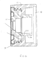
Fig. 3 is a cross-sectional side view of the same assembly; and -
Fig. 4 illustrates a modified embodiment. - Referring to the drawings, the assembly comprises a
lens barrel 10 and an imagesensor lens mount 12, each of which is typically a one-piece plastic moulding. Thelens barrel 10 holds a lens or lens assembly, and thelens mount 12 holds an image sensor chip.Fig. 3 indicates a twoelement lens assembly 14 and animage sensor chip 16; as the precise form of these is not relevant to the principles of the present invention, they are shown in outline only. Other optical elements such as filters and apertures may be mounted between thelens assembly 14 and theimage sensor chip 16. - The
lens barrel 10 andlens mount 12 are provided with mating screw threads 18a, 18b such that rotation of the lens barrel within the lens mount produces relative axial movement which can be used to focus the lens image on the light sensitive surface of thechip 16. - As best seen in
Fig. 1 , the upper part of the lens barrel is provided at its periphery with three equi-spacednotches 20 for engagement by an automated focus-setting apparatus which is known per se. The focus is set by the apparatus assessing the quality of a test image, and rotating thelens barrel 10 until optimum image quality is found. - As discussed above, we have established that during such automated focus setting particles can be shed from the engaging screw thread surfaces and impinge on the image area, leading to quality rejection of a proportion of devices.
- Referring particularly to
Fig. 3 , in the present embodiment thescrew threads 18 are radially separated from thelens assembly 14 by a formation generally designated at 22. Theformation 22 comprises an axially extendingrib 24 which extends circumferentially around the optical axis. The rib 24 interfits with acircumferential groove 26 formed in thelens barrel 10. The parts are so dimensioned that the radially outer facing surfaces of therib 24 andgroove 26 are a close sliding fit as seen at 28, while the equivalent radially inner surfaces are a clearance fit as seen at 30. - Thus, if the relative rotation of the
barrel 10 andmount 12 produces any debris from thescrew threads 18, such debris will be contained in the annular volume outside of therib 24 and cannot lodge in the optical path of the assembly. - The close fit at 28 has further advantages. It can be used to control the radial position of the lens, which can be done more accurately than by relying on the interfitting screw threads as radial location. The contact may also be made sufficiently firm as to provide resistance to relative rotation between the
lens barrel 10 and themount 12; this resistance may be used to ensure that the lens remains focussed in use, rather than applying a separate locking operation such as bonding. - Modifications of the foregoing embodiment may be made within the scope of the invention.
- For example it would be possible to have the radially inner facing surfaces of the
rib 24 andgroove 26 as a close fit, with the outer surfaces a clearance fit. - In principle, the arrangement of
Figs. 1 to 3 could also be reversed such that a rib on the lens barrel engages in a groove in the lens mount. In practice, however, this would involve increased overall size and additional material, and is therefore not preferred. -
Fig. 4 illustrates a modified embodiment in which aninner surface 32 of themount 12 is a close sliding fit against acylindrical portion 34 of thelens barrel 10. This arrangement is less desirable, by increasing the overall length, but illustrates that there are a variety of ways of isolating potential debris produced by the focussing screw threads from the optical area. - The arrangement of
Figs. 1 to 3 is, however, preferred as the sliding contact may itself produce particles (although this is less likely than with the screw thread), and inFigs. 1 to 3 such particles will be contained within thegroove 26. - The assembly of the present invention will typically be incorporated in a camera, which may itself form part of a mobile phone. The assembly may also be applied to an optical detector for an optical mouse.
Claims (7)
- A mounting assembly for positioning a lens or lens assembly relative to an image sensor chip, the mounting assembly comprising:a lens barrel adapted to hold a lens or lens assembly;a lens mount adapted to receive an image sensor chip;the lens barrel and the lens mount being provided with mating screw threads by which the lens or lens assembly may be moved along an optical axis to adjust focus on the image sensor chip;and in which the lens barrel and lens mount are additionally provided with cooperating surfaces which engage in a sliding fit in a cylindrical surface around the optical axis, said cooperating surfaces being disposed between the optical axis and the screw threads.
- A mounting assembly according to claim 1, in which said cooperating surfaces are formed on a rib formed on one of the chip mount and the lens barrel and engaging in a groove formed in the other of the chip mount and the lens barrel.
- A mounting assembly according to claim 2, in which the rib is an annular, axially extending rib on the chip mount, and the groove is an annular, axially extending groove in the lens barrel.
- A mounting assembly according to claim 3, in which a radially outer cylindrical surface of the rib is a close sliding fit upon a radially outer cylindrical surface of the groove, and a clearance fit is defined between radially inner surfaces of the rib and groove.
- A camera comprising the mounting assembly of any preceding claim.
- A mobile phone including the camera of claim 5.
- An optical mouse comprising the mounting assembly of any of claims 1 to 4.
Priority Applications (2)
| Application Number | Priority Date | Filing Date | Title |
|---|---|---|---|
| EP07119674A EP2056588B1 (en) | 2007-10-30 | 2007-10-30 | Adjustable lens mounting assembly |
| US12/191,969 US7978425B2 (en) | 2007-10-30 | 2008-08-14 | Adjustable lens mounting assembly |
Applications Claiming Priority (1)
| Application Number | Priority Date | Filing Date | Title |
|---|---|---|---|
| EP07119674A EP2056588B1 (en) | 2007-10-30 | 2007-10-30 | Adjustable lens mounting assembly |
Publications (2)
| Publication Number | Publication Date |
|---|---|
| EP2056588A1 true EP2056588A1 (en) | 2009-05-06 |
| EP2056588B1 EP2056588B1 (en) | 2012-09-26 |
Family
ID=39079615
Family Applications (1)
| Application Number | Title | Priority Date | Filing Date |
|---|---|---|---|
| EP07119674A Not-in-force EP2056588B1 (en) | 2007-10-30 | 2007-10-30 | Adjustable lens mounting assembly |
Country Status (2)
| Country | Link |
|---|---|
| US (1) | US7978425B2 (en) |
| EP (1) | EP2056588B1 (en) |
Cited By (2)
| Publication number | Priority date | Publication date | Assignee | Title |
|---|---|---|---|---|
| CN110261983A (en) * | 2019-06-04 | 2019-09-20 | 阚智博 | A kind of driving device for camera lens |
| TWI698693B (en) * | 2018-12-28 | 2020-07-11 | 大陽科技股份有限公司 | Lens assembly driving module and electronic device |
Families Citing this family (9)
| Publication number | Priority date | Publication date | Assignee | Title |
|---|---|---|---|---|
| WO2008027576A1 (en) | 2006-08-31 | 2008-03-06 | Flextronics Ap, Llc | Discreetly positionable camera housing |
| GB0910219D0 (en) * | 2009-06-15 | 2009-07-29 | St Microelectronics Res & Dev | Lens mounting assembly and method of aligning lenses in a mounting assembly |
| US8836177B2 (en) * | 2010-07-30 | 2014-09-16 | Lg Innotek Co., Ltd. | Voice coil motor |
| US8944614B2 (en) | 2011-04-29 | 2015-02-03 | xDEV, INC. | Protective cover for an electronic device |
| US8982267B2 (en) * | 2011-07-27 | 2015-03-17 | Flextronics Ap, Llc | Camera module with particle trap |
| US9071671B2 (en) * | 2012-04-06 | 2015-06-30 | Izzi Gadgets, Inc. | Cellular telephone casing system incorporating lens attachments |
| JP5850409B2 (en) * | 2012-07-25 | 2016-02-03 | 株式会社デンソーウェーブ | Optical information reader |
| WO2015122416A1 (en) * | 2014-02-12 | 2015-08-20 | 日本電産サンキョー株式会社 | Lens unit and imaging device |
| US9946909B2 (en) * | 2015-09-22 | 2018-04-17 | Symbol Technologies, Llc | Arrangement for and method of trapping debris in an electro-optical reader |
Citations (3)
| Publication number | Priority date | Publication date | Assignee | Title |
|---|---|---|---|---|
| EP1686790A1 (en) * | 2003-03-31 | 2006-08-02 | Mitsumi Electric Co., Ltd. | Image pickup unit for compact camera module |
| US20070058069A1 (en) * | 2005-09-14 | 2007-03-15 | Po-Hung Chen | Packaging structure of a light sensation module |
| DE102006049008A1 (en) * | 2005-10-17 | 2007-04-19 | Asustek Computer Inc. | Photo module that can adjust the distance between camera module and sensor unit |
Family Cites Families (2)
| Publication number | Priority date | Publication date | Assignee | Title |
|---|---|---|---|---|
| US20060103953A1 (en) * | 2004-11-15 | 2006-05-18 | Nsmc Holdings International Corp. Ltd. | Electrical micro-optic module with improved joint structures |
| KR100843300B1 (en) * | 2007-04-12 | 2008-07-03 | 삼성전기주식회사 | Camera module and its manufacturing method |
-
2007
- 2007-10-30 EP EP07119674A patent/EP2056588B1/en not_active Not-in-force
-
2008
- 2008-08-14 US US12/191,969 patent/US7978425B2/en not_active Expired - Fee Related
Patent Citations (3)
| Publication number | Priority date | Publication date | Assignee | Title |
|---|---|---|---|---|
| EP1686790A1 (en) * | 2003-03-31 | 2006-08-02 | Mitsumi Electric Co., Ltd. | Image pickup unit for compact camera module |
| US20070058069A1 (en) * | 2005-09-14 | 2007-03-15 | Po-Hung Chen | Packaging structure of a light sensation module |
| DE102006049008A1 (en) * | 2005-10-17 | 2007-04-19 | Asustek Computer Inc. | Photo module that can adjust the distance between camera module and sensor unit |
Cited By (2)
| Publication number | Priority date | Publication date | Assignee | Title |
|---|---|---|---|---|
| TWI698693B (en) * | 2018-12-28 | 2020-07-11 | 大陽科技股份有限公司 | Lens assembly driving module and electronic device |
| CN110261983A (en) * | 2019-06-04 | 2019-09-20 | 阚智博 | A kind of driving device for camera lens |
Also Published As
| Publication number | Publication date |
|---|---|
| EP2056588B1 (en) | 2012-09-26 |
| US7978425B2 (en) | 2011-07-12 |
| US20090109554A1 (en) | 2009-04-30 |
Similar Documents
| Publication | Publication Date | Title |
|---|---|---|
| US7978425B2 (en) | Adjustable lens mounting assembly | |
| RU2724459C2 (en) | Lens device, an image capturing device on which lens device can be mounted, and a camera system | |
| JP5374376B2 (en) | Camera module with contamination reduction mechanism | |
| US8305446B2 (en) | Dome type monitor camera device | |
| US20080284897A1 (en) | Camera module | |
| RU2724453C2 (en) | Lens device, an image capturing device on which a lens device can be mounted, and a camera system | |
| US12328492B2 (en) | Integrated sensor and lens assembly with post-tuning optical alignment | |
| JP4525000B2 (en) | Optical device, lens barrel and imaging device | |
| JP2006501716A (en) | How to assemble the camera module | |
| EP1465411A2 (en) | Compact camera module | |
| KR102156292B1 (en) | photographing apparatus | |
| CN112526651A (en) | Imaging lens, camera module and electronic device | |
| US7391965B2 (en) | Lens apparatus and image-taking apparatus | |
| KR20160069714A (en) | Camera module | |
| US8259224B2 (en) | Method of setting position of imaging device | |
| KR101864319B1 (en) | Security camera | |
| JP6024941B2 (en) | Lens fixing mechanism and camera device having the same | |
| KR101938002B1 (en) | Camera Module | |
| JP2010282019A (en) | Optical component and imaging device | |
| EP2112539B1 (en) | Adjustable lens mounting assembly | |
| KR100704910B1 (en) | Digital camera module | |
| KR100359133B1 (en) | Lens Assembly for a charge coupled device/complementary metal-oxide semiconductor camera having a focusing ring | |
| EP0560288B1 (en) | Light amount control apparatus and method | |
| JP2007147729A (en) | Camera module | |
| US8867152B2 (en) | Optical barrel and optical apparatus |
Legal Events
| Date | Code | Title | Description |
|---|---|---|---|
| PUAI | Public reference made under article 153(3) epc to a published international application that has entered the european phase |
Free format text: ORIGINAL CODE: 0009012 |
|
| AK | Designated contracting states |
Kind code of ref document: A1 Designated state(s): AT BE BG CH CY CZ DE DK EE ES FI FR GB GR HU IE IS IT LI LT LU LV MC MT NL PL PT RO SE SI SK TR |
|
| AX | Request for extension of the european patent |
Extension state: AL BA HR MK RS |
|
| 17P | Request for examination filed |
Effective date: 20091023 |
|
| 17Q | First examination report despatched |
Effective date: 20091118 |
|
| AKX | Designation fees paid |
Designated state(s): DE FR GB |
|
| GRAP | Despatch of communication of intention to grant a patent |
Free format text: ORIGINAL CODE: EPIDOSNIGR1 |
|
| RIN1 | Information on inventor provided before grant (corrected) |
Inventor name: CHRISTISON, ERIC |
|
| GRAS | Grant fee paid |
Free format text: ORIGINAL CODE: EPIDOSNIGR3 |
|
| GRAA | (expected) grant |
Free format text: ORIGINAL CODE: 0009210 |
|
| AK | Designated contracting states |
Kind code of ref document: B1 Designated state(s): DE FR GB |
|
| REG | Reference to a national code |
Ref country code: GB Ref legal event code: FG4D |
|
| REG | Reference to a national code |
Ref country code: DE Ref legal event code: R096 Ref document number: 602007025679 Country of ref document: DE Effective date: 20121122 |
|
| PGFP | Annual fee paid to national office [announced via postgrant information from national office to epo] |
Ref country code: GB Payment date: 20121025 Year of fee payment: 6 |
|
| PLBE | No opposition filed within time limit |
Free format text: ORIGINAL CODE: 0009261 |
|
| STAA | Information on the status of an ep patent application or granted ep patent |
Free format text: STATUS: NO OPPOSITION FILED WITHIN TIME LIMIT |
|
| 26N | No opposition filed |
Effective date: 20130627 |
|
| REG | Reference to a national code |
Ref country code: DE Ref legal event code: R097 Ref document number: 602007025679 Country of ref document: DE Effective date: 20130627 |
|
| PGFP | Annual fee paid to national office [announced via postgrant information from national office to epo] |
Ref country code: FR Payment date: 20131028 Year of fee payment: 7 Ref country code: DE Payment date: 20130920 Year of fee payment: 7 |
|
| GBPC | Gb: european patent ceased through non-payment of renewal fee |
Effective date: 20131030 |
|
| PG25 | Lapsed in a contracting state [announced via postgrant information from national office to epo] |
Ref country code: GB Free format text: LAPSE BECAUSE OF NON-PAYMENT OF DUE FEES Effective date: 20131030 |
|
| REG | Reference to a national code |
Ref country code: DE Ref legal event code: R119 Ref document number: 602007025679 Country of ref document: DE |
|
| PG25 | Lapsed in a contracting state [announced via postgrant information from national office to epo] |
Ref country code: DE Free format text: LAPSE BECAUSE OF NON-PAYMENT OF DUE FEES Effective date: 20150501 |
|
| REG | Reference to a national code |
Ref country code: FR Ref legal event code: ST Effective date: 20150630 |
|
| PG25 | Lapsed in a contracting state [announced via postgrant information from national office to epo] |
Ref country code: FR Free format text: LAPSE BECAUSE OF NON-PAYMENT OF DUE FEES Effective date: 20141031 |