EP2056338A2 - Method and system supporting production of a semiconductor device using a plurality of fabrication processes - Google Patents
Method and system supporting production of a semiconductor device using a plurality of fabrication processes Download PDFInfo
- Publication number
- EP2056338A2 EP2056338A2 EP08017659A EP08017659A EP2056338A2 EP 2056338 A2 EP2056338 A2 EP 2056338A2 EP 08017659 A EP08017659 A EP 08017659A EP 08017659 A EP08017659 A EP 08017659A EP 2056338 A2 EP2056338 A2 EP 2056338A2
- Authority
- EP
- European Patent Office
- Prior art keywords
- fabrication
- semiconductor device
- circuit
- identification
- firmware
- Prior art date
- Legal status (The legal status is an assumption and is not a legal conclusion. Google has not performed a legal analysis and makes no representation as to the accuracy of the status listed.)
- Withdrawn
Links
Images



Classifications
-
- G—PHYSICS
- G05—CONTROLLING; REGULATING
- G05B—CONTROL OR REGULATING SYSTEMS IN GENERAL; FUNCTIONAL ELEMENTS OF SUCH SYSTEMS; MONITORING OR TESTING ARRANGEMENTS FOR SUCH SYSTEMS OR ELEMENTS
- G05B19/00—Program-control systems
- G05B19/02—Program-control systems electric
- G05B19/418—Total factory control, i.e. centrally controlling a plurality of machines, e.g. direct or distributed numerical control [DNC], flexible manufacturing systems [FMS], integrated manufacturing systems [IMS] or computer integrated manufacturing [CIM]
-
- H—ELECTRICITY
- H10—SEMICONDUCTOR DEVICES; ELECTRIC SOLID-STATE DEVICES NOT OTHERWISE PROVIDED FOR
- H10P—GENERIC PROCESSES OR APPARATUS FOR THE MANUFACTURE OR TREATMENT OF DEVICES COVERED BY CLASS H10
- H10P72/00—Handling or holding of wafers, substrates or devices during manufacture or treatment thereof
- H10P72/06—Apparatus for monitoring, sorting, marking, testing or measuring
- H10P72/0604—Process monitoring, e.g. flow or thickness monitoring
-
- H—ELECTRICITY
- H10—SEMICONDUCTOR DEVICES; ELECTRIC SOLID-STATE DEVICES NOT OTHERWISE PROVIDED FOR
- H10P—GENERIC PROCESSES OR APPARATUS FOR THE MANUFACTURE OR TREATMENT OF DEVICES COVERED BY CLASS H10
- H10P72/00—Handling or holding of wafers, substrates or devices during manufacture or treatment thereof
- H10P72/06—Apparatus for monitoring, sorting, marking, testing or measuring
- H10P72/0612—Production flow monitoring, e.g. for increasing throughput
-
- H—ELECTRICITY
- H10—SEMICONDUCTOR DEVICES; ELECTRIC SOLID-STATE DEVICES NOT OTHERWISE PROVIDED FOR
- H10P—GENERIC PROCESSES OR APPARATUS FOR THE MANUFACTURE OR TREATMENT OF DEVICES COVERED BY CLASS H10
- H10P72/00—Handling or holding of wafers, substrates or devices during manufacture or treatment thereof
- H10P72/06—Apparatus for monitoring, sorting, marking, testing or measuring
- H10P72/0618—Apparatus for monitoring, sorting, marking, testing or measuring using identification means, e.g. labels on substrates or labels on containers
-
- H—ELECTRICITY
- H10—SEMICONDUCTOR DEVICES; ELECTRIC SOLID-STATE DEVICES NOT OTHERWISE PROVIDED FOR
- H10P—GENERIC PROCESSES OR APPARATUS FOR THE MANUFACTURE OR TREATMENT OF DEVICES COVERED BY CLASS H10
- H10P95/00—Generic processes or apparatus for manufacture or treatments not covered by the other groups of this subclass
Definitions
- the present invention is generally in the field of electronic circuits and systems. More specifically, the present invention is in the field of semiconductor devices and fabrication.
- RF radio frequency
- Semiconductor device 100 comprises both analog and digital circuit elements, as shown in Figure 1 .
- semiconductor device 100 includes low noise amplifier (LNA) 102 and pre-power amplifier (Pre-PA) 104.
- semiconductor device 100 includes read-only-memory (ROM) 106 storing firmware 108.
- Firmware 108 may be utilized to control the performance of semiconductor device 100 by determining values stored in registers supplying operational parameters to circuit elements. Such registers are represented on semiconductor device 100 by LNA register 112 and Pre-PA register 114, containing settings respectively for LNA 102 and Pre-PA 104.
- interface register 110 which has not been assigned a specific registry value in semiconductor device 100, and thus corresponds to a free register in the present conventional example.
- LNA 102 is shown receiving an off chip input from an unspecified device, while Pre-PA 104 is shown providing an output to an unspecified off chip device.
- the broken lines to the right of LNA 102 and Pre-PA 104, respectively, indicate the presence of other circuit components present on semiconductor device 100, but not shown in Figure 1 .
- An advantage of the conventional solution shown in Figure 1 is that operating instructions programmed into firmware 108 provide control over the performance of semiconductor device 100.
- the conventional solution provides a common set of firmware instructions that represents something of a compromise among the alternative performance profiles resulting from the slightly varying fabrication processes used to produce semiconductor device 100.
- a method and system supporting production of a semiconductor device using a plurality of fabrication processes substantially as shown in and/or described in connection with at least one of the figures, as set forth more completely in the claims.
- a tuning method for use by a semiconductor device capable of being fabricated using a plurality of fabrication processes comprises:
- the tuning is performed by a firmware corresponding to the associated fabrication process.
- the method further comprises: running a temperature compensation algorithm, the temperature compensation algorithm being selected by the semiconductor device according to the associated fabrication process.
- the fabrication identification is in a register interfacing analog and digital portions of the semiconductor device.
- the fabrication identification is in a read only memory (ROM) of the semiconductor device.
- ROM read only memory
- the semiconductor device is a radio frequency (RF) communication device.
- RF radio frequency
- the semiconductor device is utilized as a part of an electronic system, the electronic system being selected from the group consisting of a wired communications device, a wireless communications device, a cell phone, a switching device, a router, a repeater, a codec, a LAN, a WLAN, a Bluetooth enabled device, a digital camera, a digital audio player and/or recorder, a digital video player and/or recorder, a computer, a monitor, a television set, a satellite set top box, a cable modem, a digital automotive control system, a digitally-controlled home appliance, a printer, a copier, a digital audio or video receiver, an RF transceiver, a personal digital assistant (PDA), a digital game playing device, a digital testing and/or measuring device, a digital avionics device, a medical device, and a digitally-controlled medical equipment.
- PDA personal digital assistant
- a circuit capable of being patterned on a semiconductor die using a plurality of fabrication processes, the circuit comprising:
- the fabrication identification is in the interface register.
- the fabrication identification is in a read-only-memory ROM of the circuit.
- the circuit is for use in a radio frequency (RF) communications system.
- RF radio frequency
- the circuit is utilized as a part of an electronic system, the electronic system being selected from the group consisting of a wired communications device, a wireless communications device, a cell phone, a switching device, a router, a repeater, a codec, a LAN, a WLAN, a Bluetooth enabled device, a digital camera, a digital audio player and/or recorder, a digital video player and/or recorder, a computer, a monitor, a television set, a satellite set top box, a cable modem, a digital automotive control system, a digitally-controlled home appliance, a printer, a copier, a digital audio or video receiver, an RF transceiver, a personal digital assistant (PDA), a digital game playing device, a digital testing and/or measuring device, a digital avionics device, a medical device, and a digitally-controlled medical equipment.
- PDA personal digital assistant
- the circuit further comprises a read-only-memory (ROM) including a firmware, the firmware including a fabrication identification firmware corresponding to the associated fabrication process.
- ROM read-only-memory
- the fabrication identification firmware corresponding to the associated fabrication process determines settings for programmable parameters of the circuit.
- the fabrication identification firmware corresponding to the associated fabrication process determines a temperature compensation algorithm for the circuit.
- a circuit capable of being patterned on a semiconductor die using a plurality of fabrication processes, the circuit comprising:
- the fabrication identification firmware determines settings for programmable parameters of the circuit based on the associated fabrication process.
- the fabrication identification firmware determines a temperature compensation algorithm for the circuit based on the associated fabrication process
- the fabrication identification firmware determines a receiver level for the circuit based on the associated fabrication process.
- the fabrication identification firmware determines a transmitter level for the circuit based on the associated fabrication process.
- the present invention is directed to a method and system supporting production of a semiconductor device using a plurality of fabrication processes.
- the principles of the invention, as defined by the claims appended herein, can obviously be applied beyond the specifically described embodiments of the invention described herein.
- certain details have been left out in order to not obscure the inventive aspects of the invention. The details left out are within the knowledge of a person of ordinary skill in the art.
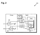
- Figure 2 shows semiconductor device 200 capable of being fabricated using a plurality of fabrication processes, according to one embodiment of the present invention. It should be noted that Figure 2 is for the purpose of providing an overview, and elements shown in Figure 2 are conceptual representations of physical and electrical elements, and are thus not intended to show dimensions or relative sizes or scale.
- FIG 2 shows semiconductor device 200 comprising both analog and digital circuit elements, analogous to semiconductor device 100, in Figure 1 .
- Semiconductor device 200 includes low noise amplifier (LNA) 202 and pre-power amplifier (Pre-PA) 204, corresponding respectively to LNA 102 and Pre-PA 104, on semiconductor device 100.
- LNA register 212 and Pre-PA register 214 are also included on semiconductor device 200, containing respective settings for LNA 202 and Pre-PA 204, corresponding respectively to LNA register 112 and Pre-PA 114, in Figure 1 .
- semiconductor device 200 includes read only memory (ROM) 206, corresponding to ROM 106, on semiconductor device 100.
- ROM read only memory
- LNA 202 is shown receiving an off chip input from an unspecified device, while Pre-PA 204 is shown providing an output to an unspecified off chip device.
- the broken lines to the right of LNA 202 and Pre-PA 204, respectively, indicate the presence of other circuit components present on semiconductor device 200, but not shown in Figure 2 .
- Semiconductor device 200 might be utilized in a cellular telephone, for example, in which implementation semiconductor device 200 might represent the "on chip" portion of a transceiver system.
- LNA 202 may receive an input, as shown in Figure 2 , from a transceiver duplexer, and the broken lines to the right of LNA 202 might indicate the presence of other receiver components.
- a signal from Pre-PA 204 may travel off semiconductor device 200 to a power amplifier, (not shown in Figure 2 ), while the broken lines to the right of Pre-PA 204 might indicate the presence of other transmitter components.
- semiconductor device 200 of Figure 2 Also included in semiconductor device 200 of Figure 2 , is fabrication identification or Fab ID 211 stored in interface register 210, and having no analogue in the conventional semiconductor device of Figure 1 . Further distinguishing semiconductor device 200 from conventional devices is the inclusion of Fab ID firmware 209 in firmware 208 for supporting Fab ID 211. As was the case for semiconductor device 100 in Figure 1 , in Figure 2 , firmware 208 may be utilized to control the performance of semiconductor device 200 by determining values stored in registers supplying operational parameters to programmable circuit elements. Unlike conventional approaches, however, in the embodiment of Figure 2 , those register values are determined according to the fabrication process used to produce semiconductor device 200 using Fab ID 211 and Fab ID firmware 209.
- semiconductor device 200 in Figure 2 , may be tuned or adjusted according to the fabrication process by which it was produced.
- semiconductor device 200 may deliver a performance optimized to a desired performance target, rather than compromised by limitations imposed by similar devices produced by alternative fabrication processes. That improvement over conventional devices is enabled in part by inclusion of Fab ID 211 in semiconductor device 200.
- the present embodiment permits semiconductor device 200 to read Fab ID 211, associate Fab ID 211 with one of a plurality of fabrication processes to determine an associated fabrication process used for fabrication of semiconductor device 200, and to tune one or more parameters according to the associated fabrication process.
- the fabricated process and its rules and parameters may be defined by fabrication labs or libraries provided by fabrication labs, such as TSMC (Taiwan Semiconductor Manufacturing Company), UMC (United Microelectronics Corporation), or other foundries.
- a temperature compensation algorithm optimized to the fabrication process producing semiconductor device 200 may also be run, in which case the temperature compensation algorithm may be selected by semiconductor device 200, according to the fabrication process associated with Fab ID 211.
- Fab ID 211 is represented as a four-bit registry entry on semiconductor device 200, in other embodiments Fab ID 211 may be encoded in a register using more, or fewer, bits. Alternatively, in one embodiment, Fab ID 211 is burned into a non-volatile memory, such as ROM 206, for example, or Fab ID 211 may be set by tying one or more bits, high or low, in interface register 210 while designing the circuits for semiconductor device 200. Furthermore, in other embodiments, semiconductor device 200 may correspond to devices other than semiconductor device 200, and may comprise any semiconductor device capable of having its performance tunably enhanced.
- Figure 3 shows flowchart 300 describing the steps, according to one embodiment of the present invention, of a tuning method for a semiconductor device capable of being fabricated using a plurality of fabrication processes.
- Certain details and features have been left out of flowchart 300 that are apparent to a person of ordinary skill in the art.
- a step may comprise one or more substeps or may involve specialized equipment or materials, as known in the art.
- steps 310 through 340 indicated in flowchart 300 are sufficient to describe one embodiment of the present invention, other embodiments of the invention may utilize steps different from those shown in flowchart 300.
- step 310 of flowchart 300 comprises reading interface register 210 included in semiconductor device 200.
- step 310 is shown by the connection between firmware 208 and interface register 210 in which Fab ID 211 is stored.
- Fab ID 211 may be recorded elsewhere for reading by semiconductor device 200, for example, Fab ID 211 may be stored in ROM 206.
- Reading Fab ID 211 provides a criterion allowing semiconductor device 200 to be distinguished from substantially matching devices made by a different fabrication process.
- step 320 of flowchart 300 comprises associating Fab ID 211 with one of a plurality of fabrication processes to determine a fabrication process used to fabricate semiconductor device 200. Association of semiconductor device 200 with the fabrication process used to produce it enables determination of programmable parameters for adjusting the performance of semiconductor device 200 to a desired standard.
- Step 330 of flowchart 300 comprises tuning at least one programmable parameter of semiconductor device 200 according to settings corresponding to the associated fabrication process.
- step 330 is represented by the presence of Fab ID firmware 209 included in firmware 208.
- association of Fab ID 211 with one of a plurality of fabrication processes in step 320 allows selection of corresponding Fab ID firmware 209 retrieving programmable settings corresponding to the associated fabrication process.
- tuning of programmable parameters could be determined by settings provided by Fab ID firmware 209, corresponding with the fabrication process used to produce semiconductor device 200.
- tuning step 330 is represented as being performed by Fab ID firmware 209
- associating a fabrication identification with a fabrication process may include designation of a programmable parameter database corresponding to the fabrication process.
- tuning may be performed by a common firmware, such as firmware 108 in Figure 1 , with appropriate importation of fabrication process specific parameter settings from the designated database, for example.
- step 340 comprises running a temperature compensation algorithm corresponding with the associated fabrication process.
- different fabrication processes may produce subtlely distinct performance profiles that may be brought into alignment by the tuning of programmable parameters, those different fabrication processes my result in varying temperature response profiles among a family of semiconductor devices as well. Even where, for example, performance parameters of semiconductor devices produced by different fabrication processes are substantially identical, their temperature response may not be, so that performance stability may vary among those devices.
- Step 340 may be performed to address that possibility by applying a temperature compensation algorithm specific to the fabrication process used for production of the semiconductor device.
- Other performance parameters that can be tuned by Fab ID firmware 208 may include transmitter and receiver high and low dB levels in the analog portion of the semiconductor device 200.
- a semiconductor device can be prepared for use and implemented.
- FIG. 4 is a diagram of an exemplary electronic system including an exemplary semiconductor device capable of being fabricated using a plurality of fabrication processes, in accordance with one or more embodiments of the present invention.
- Electronic system 400 includes exemplary modules 402, 404, and 406, semiconductor device 408, discrete components 410 and 412, residing in and interconnected through electronic system 400, for example, through a circuit board.
- Semiconductor device 408, in Figure 4 includes circuit 416, which can be a microprocessor, for instance.
- electronic system 400 is shown to include exemplary modules 402, 404, and 406, and discrete components 410 and 412, in addition to semiconductor device 408, in one embodiment electronic system 400 may be implemented as a System-on-a-Chip (SoC), for example.
- SoC System-on-a-Chip
- modules 402, 404, and 406 are included in electronic system 400 and can each be, for example, a central processing unit (CPU), a graphics controller, a digital signal processor (DSP), an application specific integrated circuit (ASIC), a video processing module, an audio processing module, a radio frequency (RF) receiver, an RF transmitter, an image sensor module, a power control module, an electromechanical motor control module, or a field programmable gate array (FPGA), or any other kind of module utilized in modem electronic systems.
- Electronic system 400 can include a number of interconnects (not shown in Figure 4 ) for interconnecting modules 402, 404, and 406, discrete components 410 and 412, and semiconductor device 408.
- discrete components 410 and 412 are included in electronic system 400 and can each be, for example, a discrete filter, such as one including a BAW or SAW filter or the like, a power amplifier or an operational amplifier, an additional semiconductor device, an antenna element, an inductor, a capacitor, or a resistor.
- Electronic system 400 can be utilized in, for example, a wired communications device, a wireless communications device, a cell phone, a switching device, a router, a repeater, a codec, a LAN, a WLAN, a Bluetooth enabled device, a digital camera, a digital audio player and/or recorder, a digital video player and/or recorder, a computer, a monitor, a television set, a satellite set top box, a cable modem, a digital automotive control system, a digitally-controlled home appliance, a printer, a copier, a digital audio or video receiver, an RF transceiver, a personal digital assistant (PDA), a digital game playing device, a digital testing and/or measuring device, a digital avionics device, a medical device, or a digitally-controlled medical equipment, or in any other kind of system, device, component or module utilized in modem electronics applications.
- PDA personal digital assistant
- the present application discloses a method and system supporting production of a semiconductor device using a plurality of fabrication processes.
- a semiconductor device read a fabrication identification recorded in itself
- one embodiment of the present invention enables identification of the fabrication process by which the semiconductor device was produced, from among a plurality of possible alternatives.
- performance characteristics including temperature response, for example, with an identified fabrication process
- one embodiment of the present invention permits fabrication process specific tuning and performance management of a semiconductor device, advantageously improving adherence to desired performance specifications.
Landscapes
- Engineering & Computer Science (AREA)
- General Engineering & Computer Science (AREA)
- Manufacturing & Machinery (AREA)
- Quality & Reliability (AREA)
- Physics & Mathematics (AREA)
- General Physics & Mathematics (AREA)
- Automation & Control Theory (AREA)
- Semiconductor Integrated Circuits (AREA)
- Thin Film Transistor (AREA)
Abstract
Description
- The present invention is generally in the field of electronic circuits and systems. More specifically, the present invention is in the field of semiconductor devices and fabrication.
- Electronic devices and systems have become an essential staple of modern existence, utilized in virtually every aspect of life, from increasing personal communications options, to enhancing workplace productivity, and even expanding the definition of workplace. As products such as personal computers, mobile telephones, navigational systems, and hands free communications devices become more sophisticated and, perhaps counter intuitively, easier to use, our reliance upon them grows. Consequently, what once were considered tools of convenience are increasingly seen as resources of necessity, and that trend has continued strongly.
- The combined effects of increasing device complexity and growing consumer demand places considerable strain on the businesses that deliver sophisticated electronic products to the marketplace. On one hand, high demand produces an attractive commercial environment for those enterprises, encouraging others to enter the marketplace and compete for consumer affections. The resulting competition among product providers makes managing production costs crucial to their continued competitiveness. At the same time, however, the increased complexity of the component devices and sub-systems on which these sophisticated electronic products rely almost compels specialization by the suppliers of those component elements. As a result, a provider of cellular telephones, for example, must typically form alliances with suppliers of key cellular telephone components, such as semiconductor device components, and those semiconductor device suppliers may in turn rely upon semiconductor fabrication facilities utilizing various fabrication processes to produce the semiconductor devices they supply.
- For a supplier delivering a product that depends on upstream component fabrication, access to more than one fabrication source for an essential component may be desirable. Having more than one source for essential components presents multiple advantages. First, having a choice amongst alternative fabrication sources producing the same component gives a business leverage to minimize component costs, which may be essential to its own competitiveness. Secondly, reliance on more than one fabrication source makes a supplier less vulnerable to production failures by any single facility. In addition, reliance on more than one fabrication source increases available production capacity, in case of a sudden spike in demand.
- Although access to more than one fabrication source provides several advantages, as described, it also poses challenges for a supplier seeking to deliver consistent product performance while incorporating components from distinct sources. The challenge can be particularly great for suppliers of radio frequency (RF) communication product components, for example, where even minor variations in component performance can deleteriously effect overall system performance. For instance, the performance of a cellular telephone may depend on the performance of a component sub-system, which may itself be dependent on the performance of a semiconductor device. Where an integrated circuit chip is produced using multiple fabrication processes, the chip supplier must compensate for small variations in performance of the chips produced by the different fabrication processes, in order to supply a consistent product to a cellular telephone provider.
- Conventional solutions for assuring consistent performance from semiconductor devices fabricated using multiple fabrication processes, for example, may include implementation of operating instructions that take into consideration variations in performance among the devices produced by the different fabrication processes. One such solution is presented in
Figure 1 , which shows a conventional semiconductor device, provided to support an RF communication system, for example. -
Semiconductor device 100 comprises both analog and digital circuit elements, as shown inFigure 1 . On the analog side,semiconductor device 100 includes low noise amplifier (LNA) 102 and pre-power amplifier (Pre-PA) 104. On the digital side,semiconductor device 100 includes read-only-memory (ROM) 106storing firmware 108.Firmware 108 may be utilized to control the performance ofsemiconductor device 100 by determining values stored in registers supplying operational parameters to circuit elements. Such registers are represented onsemiconductor device 100 by LNAregister 112 and Pre-PAregister 114, containing settings respectively for LNA 102 and Pre-PA 104. Also shown inFigure 1 isinterface register 110, which has not been assigned a specific registry value insemiconductor device 100, and thus corresponds to a free register in the present conventional example. InFigure 1 , LNA 102 is shown receiving an off chip input from an unspecified device, while Pre-PA 104 is shown providing an output to an unspecified off chip device. The broken lines to the right of LNA 102 and Pre-PA 104, respectively, indicate the presence of other circuit components present onsemiconductor device 100, but not shown inFigure 1 . - An advantage of the conventional solution shown in
Figure 1 is that operating instructions programmed intofirmware 108 provide control over the performance ofsemiconductor device 100. The conventional solution provides a common set of firmware instructions that represents something of a compromise among the alternative performance profiles resulting from the slightly varying fabrication processes used to producesemiconductor device 100. Therein lies a significant disadvantage of the conventional solution as well. Becausesemiconductor device 100 is tuned to provide a uniform level of performance achievable by chips fabricated using each fabrication process utilized by a different fabrication source, it is typically the spectrum of achievable performance parameters that determines the selected tuning values, rather than the optimum performance of a single version ofsemiconductor device 100, or the performance parameters most advantageous to end user performance of a system utilizingsemiconductor device 100. - Thus, there is a need to overcome the drawbacks and deficiencies in the art to enable determination of tuning parameters for a semiconductor device according to the fabrication process used to produce it.
- A method and system supporting production of a semiconductor device using a plurality of fabrication processes, substantially as shown in and/or described in connection with at least one of the figures, as set forth more completely in the claims.
- According to an aspect, a tuning method for use by a semiconductor device capable of being fabricated using a plurality of fabrication processes comprises:
- reading by the semiconductor device, a fabrication identification included in the semiconductor device;
- associating the fabrication identification with one of the plurality of fabrication processes to determine an associated fabrication process used for fabrication of the semiconductor device; and
- tuning at least one parameter of the semiconductor device based on the associated fabrication process.
- Advantageously, the tuning is performed by a firmware corresponding to the associated fabrication process.
- Advantageously, the method further comprises: running a temperature compensation algorithm, the temperature compensation algorithm being selected by the semiconductor device according to the associated fabrication process.
- Advantageously, the fabrication identification is in a register interfacing analog and digital portions of the semiconductor device.
- Advantageously, the fabrication identification is in a read only memory (ROM) of the semiconductor device.
- Advantageously, the semiconductor device is a radio frequency (RF) communication device.
- Advantageously, the semiconductor device is utilized as a part of an electronic system, the electronic system being selected from the group consisting of a wired communications device, a wireless communications device, a cell phone, a switching device, a router, a repeater, a codec, a LAN, a WLAN, a Bluetooth enabled device, a digital camera, a digital audio player and/or recorder, a digital video player and/or recorder, a computer, a monitor, a television set, a satellite set top box, a cable modem, a digital automotive control system, a digitally-controlled home appliance, a printer, a copier, a digital audio or video receiver, an RF transceiver, a personal digital assistant (PDA), a digital game playing device, a digital testing and/or measuring device, a digital avionics device, a medical device, and a digitally-controlled medical equipment.
- According to an aspect, a circuit is provided capable of being patterned on a semiconductor die using a plurality of fabrication processes, the circuit comprising:
- a digital circuitry;
- an analog circuitry;
- a fabrication identification, wherein the fabrication associates the circuit with one of the plurality of fabrication processes used for fabrication of the circuit; and
- an interface circuitry interfacing the digital circuitry with the analog circuitry, the interface circuitry for use by the digital circuitry to tune the analog circuitry based on the fabrication identification.
- Advantageously, the fabrication identification is in the interface register.
- Advantageously, the fabrication identification is in a read-only-memory ROM of the circuit.
- Advantageously, the circuit is for use in a radio frequency (RF) communications system.
- Advantageously, the circuit is utilized as a part of an electronic system, the electronic system being selected from the group consisting of a wired communications device, a wireless communications device, a cell phone, a switching device, a router, a repeater, a codec, a LAN, a WLAN, a Bluetooth enabled device, a digital camera, a digital audio player and/or recorder, a digital video player and/or recorder, a computer, a monitor, a television set, a satellite set top box, a cable modem, a digital automotive control system, a digitally-controlled home appliance, a printer, a copier, a digital audio or video receiver, an RF transceiver, a personal digital assistant (PDA), a digital game playing device, a digital testing and/or measuring device, a digital avionics device, a medical device, and a digitally-controlled medical equipment.
- Advantageously, the circuit further comprises a read-only-memory (ROM) including a firmware, the firmware including a fabrication identification firmware corresponding to the associated fabrication process.
- Advantageously, the fabrication identification firmware corresponding to the associated fabrication process determines settings for programmable parameters of the circuit.
- Advantageously, the fabrication identification firmware corresponding to the associated fabrication process determines a temperature compensation algorithm for the circuit.
- According to an aspect, a circuit is provided capable of being patterned on a semiconductor die using a plurality of fabrication processes, the circuit comprising:
- a fabrication identification, wherein the fabrication associates the circuit with one of the plurality of fabrication processes used for fabrication of the circuit; and
- a read-only-memory (ROM);
- a fabrication identification firmware in the ROM, the fabrication identification firmware designed to read the fabrication identification and associate the fabrication identification with one of plurality of fabrication processes to determine an associated fabrication process, the fabrication identification firmware further designed to tune the circuit based on the associated fabrication process.
- Advantageously, the fabrication identification firmware determines settings for programmable parameters of the circuit based on the associated fabrication process.
- Advantageously, the fabrication identification firmware determines a temperature compensation algorithm for the circuit based on the associated fabrication process
- Advantageously, the fabrication identification firmware determines a receiver level for the circuit based on the associated fabrication process.
- Advantageously, the fabrication identification firmware determines a transmitter level for the circuit based on the associated fabrication process.
- The features and advantages of the present invention will become more readily apparent to those ordinarily skilled in the art after reviewing the following detailed description and accompanying drawings, wherein:
-
Figure 1 shows a conventional semiconductor device; -
Figure 2 shows a semiconductor device capable of being fabricated using a plurality of fabrication processes, according to on embodiment of the present invention; -
Figure 3 is a flowchart presenting a tuning method for a semiconductor device capable of being fabricated using a plurality of fabrication processes, according to one embodiment of the present invention; and -
Figure 4 is a diagram of an exemplary electronic system including an exemplary semiconductor device capable of being fabricated using a plurality of fabrication processes, in accordance with one or more embodiments of the present invention. - The present invention is directed to a method and system supporting production of a semiconductor device using a plurality of fabrication processes. Although the invention is described with respect to specific embodiments, the principles of the invention, as defined by the claims appended herein, can obviously be applied beyond the specifically described embodiments of the invention described herein. Moreover, in the description of the present invention, certain details have been left out in order to not obscure the inventive aspects of the invention. The details left out are within the knowledge of a person of ordinary skill in the art.
- The drawings in the present application and their accompanying detailed description are directed to merely example embodiments of the invention. To maintain brevity, other embodiments of the invention, which use the principles of the present invention, are not specifically described in the present application and are not specifically illustrated by the present drawings. It should be borne in mind that, unless noted otherwise, like or corresponding elements among the figures may be indicated by like or corresponding reference numerals.
-
Figure 2 showssemiconductor device 200 capable of being fabricated using a plurality of fabrication processes, according to one embodiment of the present invention. It should be noted thatFigure 2 is for the purpose of providing an overview, and elements shown inFigure 2 are conceptual representations of physical and electrical elements, and are thus not intended to show dimensions or relative sizes or scale. -
Figure 2 showssemiconductor device 200 comprising both analog and digital circuit elements, analogous tosemiconductor device 100, inFigure 1 .Semiconductor device 200 includes low noise amplifier (LNA) 202 and pre-power amplifier (Pre-PA) 204, corresponding respectively toLNA 102 andPre-PA 104, onsemiconductor device 100. Also included onsemiconductor device 200 areLNA register 212 andPre-PA register 214, containing respective settings forLNA 202 andPre-PA 204, corresponding respectively to LNA register 112 andPre-PA 114, inFigure 1 . Moreover,semiconductor device 200 includes read only memory (ROM) 206, corresponding toROM 106, onsemiconductor device 100. - In
Figure 2 ,LNA 202 is shown receiving an off chip input from an unspecified device, whilePre-PA 204 is shown providing an output to an unspecified off chip device. The broken lines to the right ofLNA 202 andPre-PA 204, respectively, indicate the presence of other circuit components present onsemiconductor device 200, but not shown inFigure 2 .Semiconductor device 200 might be utilized in a cellular telephone, for example, in whichimplementation semiconductor device 200 might represent the "on chip" portion of a transceiver system. In thatcase LNA 202 may receive an input, as shown inFigure 2 , from a transceiver duplexer, and the broken lines to the right ofLNA 202 might indicate the presence of other receiver components. Moreover, in that instance, a signal fromPre-PA 204 may travel offsemiconductor device 200 to a power amplifier, (not shown inFigure 2 ), while the broken lines to the right ofPre-PA 204 might indicate the presence of other transmitter components. - Also included in
semiconductor device 200 ofFigure 2 , is fabrication identification orFab ID 211 stored in interface register 210, and having no analogue in the conventional semiconductor device ofFigure 1 . Further distinguishingsemiconductor device 200 from conventional devices is the inclusion ofFab ID firmware 209 infirmware 208 for supportingFab ID 211. As was the case forsemiconductor device 100 inFigure 1 , inFigure 2 ,firmware 208 may be utilized to control the performance ofsemiconductor device 200 by determining values stored in registers supplying operational parameters to programmable circuit elements. Unlike conventional approaches, however, in the embodiment ofFigure 2 , those register values are determined according to the fabrication process used to producesemiconductor device 200 usingFab ID 211 andFab ID firmware 209. - In effect, the performance of
semiconductor device 200, inFigure 2 , may be tuned or adjusted according to the fabrication process by which it was produced. As a result,semiconductor device 200 may deliver a performance optimized to a desired performance target, rather than compromised by limitations imposed by similar devices produced by alternative fabrication processes. That improvement over conventional devices is enabled in part by inclusion ofFab ID 211 insemiconductor device 200. - By including
Fab ID 211, e.g., four bits having the permanent value of"0010", insemiconductor device 200, the present embodiment permitssemiconductor device 200 to readFab ID 211,associate Fab ID 211 with one of a plurality of fabrication processes to determine an associated fabrication process used for fabrication ofsemiconductor device 200, and to tune one or more parameters according to the associated fabrication process. In one embodiment, the fabricated process and its rules and parameters may be defined by fabrication labs or libraries provided by fabrication labs, such as TSMC (Taiwan Semiconductor Manufacturing Company), UMC (United Microelectronics Corporation), or other foundries. In one embodiment, a temperature compensation algorithm optimized to the fabrication process producingsemiconductor device 200 may also be run, in which case the temperature compensation algorithm may be selected bysemiconductor device 200, according to the fabrication process associated withFab ID 211. - Although in the present embodiment,
Fab ID 211 is represented as a four-bit registry entry onsemiconductor device 200, in other embodimentsFab ID 211 may be encoded in a register using more, or fewer, bits. Alternatively, in one embodiment,Fab ID 211 is burned into a non-volatile memory, such asROM 206, for example, orFab ID 211 may be set by tying one or more bits, high or low, in interface register 210 while designing the circuits forsemiconductor device 200. Furthermore, in other embodiments,semiconductor device 200 may correspond to devices other thansemiconductor device 200, and may comprise any semiconductor device capable of having its performance tunably enhanced. - Turning now to
Figure 3, Figure 3 showsflowchart 300 describing the steps, according to one embodiment of the present invention, of a tuning method for a semiconductor device capable of being fabricated using a plurality of fabrication processes. Certain details and features have been left out offlowchart 300 that are apparent to a person of ordinary skill in the art. For example, a step may comprise one or more substeps or may involve specialized equipment or materials, as known in the art. Whilesteps 310 through 340 indicated inflowchart 300 are sufficient to describe one embodiment of the present invention, other embodiments of the invention may utilize steps different from those shown inflowchart 300. - Referring to the steps of
flowchart 300 inFigure 3 , in conjunction withFigure 2 , step 310 offlowchart 300 comprises reading interface register 210 included insemiconductor device 200. InFigure 2 ,step 310 is shown by the connection betweenfirmware 208 and interface register 210 in whichFab ID 211 is stored. As discussed in relation toFigure 2 , in other embodimentsFab ID 211 may be recorded elsewhere for reading bysemiconductor device 200, for example,Fab ID 211 may be stored inROM 206.Reading Fab ID 211 provides a criterion allowingsemiconductor device 200 to be distinguished from substantially matching devices made by a different fabrication process. - Continuing with
step 320 ofFigure 3 , step 320 offlowchart 300 comprises associatingFab ID 211 with one of a plurality of fabrication processes to determine a fabrication process used to fabricatesemiconductor device 200. Association ofsemiconductor device 200 with the fabrication process used to produce it enables determination of programmable parameters for adjusting the performance ofsemiconductor device 200 to a desired standard. - Step 330 of
flowchart 300 comprises tuning at least one programmable parameter ofsemiconductor device 200 according to settings corresponding to the associated fabrication process. In the embodiment ofFigure 2 ,step 330 is represented by the presence ofFab ID firmware 209 included infirmware 208. In that example, association ofFab ID 211 with one of a plurality of fabrication processes instep 320, allows selection of correspondingFab ID firmware 209 retrieving programmable settings corresponding to the associated fabrication process. Continuing with the embodiment ofFigure 2 , where, for example, step 310 had read "0001" fromFab ID 211 rather than "0010" in interface register 210, tuning of programmable parameters could be determined by settings provided byFab ID firmware 209, corresponding with the fabrication process used to producesemiconductor device 200. - Although in the embodiment shown in
Figure 2 , tuningstep 330 is represented as being performed byFab ID firmware 209, in another embodiment, associating a fabrication identification with a fabrication process may include designation of a programmable parameter database corresponding to the fabrication process. In that embodiment, tuning may be performed by a common firmware, such asfirmware 108 inFigure 1 , with appropriate importation of fabrication process specific parameter settings from the designated database, for example. - Continuing with
step 340 offlowchart 300,step 340 comprises running a temperature compensation algorithm corresponding with the associated fabrication process. Just as different fabrication processes may produce subtlely distinct performance profiles that may be brought into alignment by the tuning of programmable parameters, those different fabrication processes my result in varying temperature response profiles among a family of semiconductor devices as well. Even where, for example, performance parameters of semiconductor devices produced by different fabrication processes are substantially identical, their temperature response may not be, so that performance stability may vary among those devices. Step 340 may be performed to address that possibility by applying a temperature compensation algorithm specific to the fabrication process used for production of the semiconductor device. Other performance parameters that can be tuned byFab ID firmware 208 may include transmitter and receiver high and low dB levels in the analog portion of thesemiconductor device 200. - As a result of the tuning method for a semiconductor device capable of being fabricated using a plurality of fabrication processes, described in the exemplary embodiments set forth in the present application and shown by
flowchart 300 inFigure 3 , a semiconductor device can be prepared for use and implemented. -
Figure 4 is a diagram of an exemplary electronic system including an exemplary semiconductor device capable of being fabricated using a plurality of fabrication processes, in accordance with one or more embodiments of the present invention.Electronic system 400 includesexemplary modules semiconductor device 408,discrete components electronic system 400, for example, through a circuit board.Semiconductor device 408, inFigure 4 , includescircuit 416, which can be a microprocessor, for instance. Although in the present embodimentelectronic system 400 is shown to includeexemplary modules discrete components semiconductor device 408, in one embodimentelectronic system 400 may be implemented as a System-on-a-Chip (SoC), for example. - As shown in
Figure 4 ,modules electronic system 400 and can each be, for example, a central processing unit (CPU), a graphics controller, a digital signal processor (DSP), an application specific integrated circuit (ASIC), a video processing module, an audio processing module, a radio frequency (RF) receiver, an RF transmitter, an image sensor module, a power control module, an electromechanical motor control module, or a field programmable gate array (FPGA), or any other kind of module utilized in modem electronic systems.Electronic system 400 can include a number of interconnects (not shown inFigure 4 ) for interconnectingmodules discrete components semiconductor device 408. Also shown inFigure 4 ,discrete components electronic system 400 and can each be, for example, a discrete filter, such as one including a BAW or SAW filter or the like, a power amplifier or an operational amplifier, an additional semiconductor device, an antenna element, an inductor, a capacitor, or a resistor. -
Electronic system 400 can be utilized in, for example, a wired communications device, a wireless communications device, a cell phone, a switching device, a router, a repeater, a codec, a LAN, a WLAN, a Bluetooth enabled device, a digital camera, a digital audio player and/or recorder, a digital video player and/or recorder, a computer, a monitor, a television set, a satellite set top box, a cable modem, a digital automotive control system, a digitally-controlled home appliance, a printer, a copier, a digital audio or video receiver, an RF transceiver, a personal digital assistant (PDA), a digital game playing device, a digital testing and/or measuring device, a digital avionics device, a medical device, or a digitally-controlled medical equipment, or in any other kind of system, device, component or module utilized in modem electronics applications. - Thus, the present application discloses a method and system supporting production of a semiconductor device using a plurality of fabrication processes. By having a semiconductor device read a fabrication identification recorded in itself, one embodiment of the present invention enables identification of the fabrication process by which the semiconductor device was produced, from among a plurality of possible alternatives. By further associating performance characteristics, including temperature response, for example, with an identified fabrication process, one embodiment of the present invention permits fabrication process specific tuning and performance management of a semiconductor device, advantageously improving adherence to desired performance specifications.
- From the above description of the invention it is manifest that various techniques can be used for implementing the concepts of the present invention without departing from its scope. Moreover, while the invention has been described with specific reference to certain embodiments, a person of ordinary skill in the art would recognize that changes can be made in form and detail without departing from the spirit and the scope of the invention. The described embodiments are to be considered in all respects as illustrative and not restrictive. It should also be understood that the invention is not limited to the particular embodiments described herein, but is capable of many rearrangements, modifications, and substitutions without departing from the scope of the invention.
Claims (10)
- A tuning method for use by a semiconductor device capable of being fabricated using a plurality of fabrication processes, the method comprising:reading by the semiconductor device, a fabrication identification included in the semiconductor device;associating the fabrication identification with one of the plurality of fabrication processes to determine an associated fabrication process used for fabrication of the semiconductor device; andtuning at least one parameter of the semiconductor device based on the associated fabrication process.
- The tuning method of claim 1, wherein the tuning is performed by a firmware corresponding to the associated fabrication process.
- The tuning method of claim 1 further comprising: running a temperature compensation algorithm, the temperature compensation algorithm being selected by the semiconductor device according to the associated fabrication process.
- The tuning method of claim 1, wherein the fabrication identification is in a register interfacing analog and digital portions of the semiconductor device.
- The tuning method of claim 1, wherein the fabrication identification is in a read only memory (ROM) of the semiconductor device.
- A circuit capable of being patterned on a semiconductor die using a plurality of fabrication processes, the circuit comprising:a digital circuitry;an analog circuitry;a fabrication identification, wherein the fabrication associates the circuit with one of the plurality of fabrication processes used for fabrication of the circuit; andan interface circuitry interfacing the digital circuitry with the analog circuitry, the interface circuitry for use by the digital circuitry to tune the analog circuitry based on the fabrication identification.
- The circuit of claim 6, wherein the fabrication identification is in the interface register.
- The circuit of claim 6, wherein the fabrication identification is in a read-only-memory ROM of the circuit.
- The circuit of claim 6, wherein the circuit is for use in a radio frequency (RF) communications system.
- A circuit capable of being patterned on a semiconductor die using a plurality of fabrication processes, the circuit comprising:a fabrication identification, wherein the fabrication associates the circuit with one of the plurality of fabrication processes used for fabrication of the circuit; anda read-only-memory (ROM);a fabrication identification firmware in the ROM, the fabrication identification firmware designed to read the fabrication identification and associate the fabrication identification with one of plurality of fabrication processes to determine an associated fabrication process, the fabrication identification firmware further designed to tune the circuit based on the associated fabrication process.
Applications Claiming Priority (1)
| Application Number | Priority Date | Filing Date | Title |
|---|---|---|---|
| US12/001,214 US20090146144A1 (en) | 2007-12-10 | 2007-12-10 | Method and system supporting production of a semiconductor device using a plurality of fabrication processes |
Publications (2)
| Publication Number | Publication Date |
|---|---|
| EP2056338A2 true EP2056338A2 (en) | 2009-05-06 |
| EP2056338A3 EP2056338A3 (en) | 2013-03-06 |
Family
ID=40467264
Family Applications (1)
| Application Number | Title | Priority Date | Filing Date |
|---|---|---|---|
| EP08017659A Withdrawn EP2056338A3 (en) | 2007-12-10 | 2008-10-08 | Method and system supporting production of a semiconductor device using a plurality of fabrication processes |
Country Status (5)
| Country | Link |
|---|---|
| US (1) | US20090146144A1 (en) |
| EP (1) | EP2056338A3 (en) |
| KR (1) | KR20090060959A (en) |
| CN (1) | CN101471626B (en) |
| TW (1) | TW200949477A (en) |
Families Citing this family (1)
| Publication number | Priority date | Publication date | Assignee | Title |
|---|---|---|---|---|
| CN110471801A (en) * | 2019-06-20 | 2019-11-19 | 深圳市德名利电子有限公司 | A kind of management method and device and equipment of the volume production procedural information storing equipment |
Family Cites Families (23)
| Publication number | Priority date | Publication date | Assignee | Title |
|---|---|---|---|---|
| US5729158A (en) * | 1995-07-07 | 1998-03-17 | Sun Microsystems, Inc. | Parametric tuning of an integrated circuit after fabrication |
| US6259957B1 (en) * | 1997-04-04 | 2001-07-10 | Cirrus Logic, Inc. | Circuits and methods for implementing audio Codecs and systems using the same |
| US6347258B1 (en) * | 1999-09-23 | 2002-02-12 | Taiwan Semiconductor Manufacturing Co., Ltd. | Data structure of a product technology and a method of preparing the same |
| US7106388B2 (en) * | 1999-12-15 | 2006-09-12 | Broadcom Corporation | Digital IF demodulator for video applications |
| US6885853B2 (en) * | 2001-04-11 | 2005-04-26 | National Scientific Corporation | Communications receiver with integrated IF filter and method therefor |
| US20040051815A1 (en) * | 2001-06-05 | 2004-03-18 | Alpaiwalia Feroz Kaiki | Apparatus for providing tuner parameters in a television receiver |
| US7003656B2 (en) * | 2002-06-13 | 2006-02-21 | Hewlett-Packard Development Company, L.P. | Automatic selection of firmware for a computer that allows a plurality of process types |
| US6952623B2 (en) * | 2002-07-02 | 2005-10-04 | Texas Instruments, Inc. | Permanent chip ID using FeRAM |
| JP2004040626A (en) * | 2002-07-05 | 2004-02-05 | Sanyo Electric Co Ltd | Temperature compensating device of semiconductor integrated circuit |
| US7166826B1 (en) * | 2002-11-13 | 2007-01-23 | Micrel, Incorporated | Automatic control of laser diode current and optical power output |
| US7309998B2 (en) * | 2002-12-02 | 2007-12-18 | Burns Lawrence M | Process monitor for monitoring an integrated circuit chip |
| US7246222B2 (en) * | 2003-04-21 | 2007-07-17 | Hewlett-Packard Development Company, L.P. | Processor type determination based on reset vector characteristics |
| US7113422B2 (en) * | 2003-11-30 | 2006-09-26 | Union Semiconductor Technology Corporation | Method for optimizing MRAM circuit performance |
| US7248124B2 (en) * | 2004-03-22 | 2007-07-24 | Mobius Microsystems, Inc. | Frequency calibration for a monolithic clock generator and timing/frequency reference |
| US7308655B2 (en) * | 2004-03-25 | 2007-12-11 | Taiwan Semiconductor Manufacturing Company, Ltd. | Method and system for alerting an entity to design changes impacting the manufacture of a semiconductor device in a virtual fab environment |
| JP4721689B2 (en) * | 2004-10-28 | 2011-07-13 | 富士通周辺機株式会社 | Method for installing firmware in electronic equipment and printed circuit board |
| US7693491B2 (en) * | 2004-11-30 | 2010-04-06 | Broadcom Corporation | Method and system for transmitter output power compensation |
| US7665661B2 (en) * | 2005-03-28 | 2010-02-23 | R828 Llc | Secure system for tracking elements using tags |
| KR100827766B1 (en) * | 2005-06-28 | 2008-05-07 | 삼성전자주식회사 | Method and system for initial procedure in a frequency overlay communication system |
| US20070162964A1 (en) * | 2006-01-12 | 2007-07-12 | Wang Liang-Yun | Embedded system insuring security and integrity, and method of increasing security thereof |
| US7714783B2 (en) * | 2007-08-02 | 2010-05-11 | Samsung Electronics Co., Ltd. | Method and system for analog beamforming in wireless communications |
| JP2009049813A (en) * | 2007-08-21 | 2009-03-05 | Sanyo Electric Co Ltd | Semiconductor device for radio tuner and manufacturing method thereof |
| US8131232B2 (en) * | 2009-10-09 | 2012-03-06 | Texas Instruments Incorporated | Method and apparatus for antenna tuning |
-
2007
- 2007-12-10 US US12/001,214 patent/US20090146144A1/en not_active Abandoned
-
2008
- 2008-10-08 EP EP08017659A patent/EP2056338A3/en not_active Withdrawn
- 2008-11-28 CN CN2008101816793A patent/CN101471626B/en active Active
- 2008-12-10 KR KR1020080125216A patent/KR20090060959A/en not_active Ceased
- 2008-12-10 TW TW097148043A patent/TW200949477A/en unknown
Also Published As
| Publication number | Publication date |
|---|---|
| KR20090060959A (en) | 2009-06-15 |
| TW200949477A (en) | 2009-12-01 |
| CN101471626B (en) | 2012-12-12 |
| US20090146144A1 (en) | 2009-06-11 |
| EP2056338A3 (en) | 2013-03-06 |
| CN101471626A (en) | 2009-07-01 |
| HK1135522A1 (en) | 2010-06-04 |
Similar Documents
| Publication | Publication Date | Title |
|---|---|---|
| CN104242876B (en) | For fine-tuning passive component on the tube core of a large amount of manufactures | |
| US7925463B2 (en) | Method and system for compensating temperature readings from a temperature sensing crystal integrated circuit | |
| EP1931051B1 (en) | Method and system for single chip WLAN and Bluetooth radios on a single CMOS substrate | |
| TW201008110A (en) | Method of achieving high selectivity in receiver RF front-ends | |
| US20080207240A1 (en) | Auto-calibrating receiver and methods for use therewith | |
| KR20130047636A (en) | Rf transceiver with calibrated pre-distortion and methods for use therewith | |
| WO2010108029A1 (en) | Transconductance bias circuit, amplifier and method | |
| US8731501B2 (en) | Systems and methods for tuning a broadcast radio receiver with digital display | |
| JP2019506079A (en) | Transformer in voltage-controlled oscillator of wireless sensor device | |
| US20090146144A1 (en) | Method and system supporting production of a semiconductor device using a plurality of fabrication processes | |
| US20130226496A1 (en) | Precise calibration of electronic components | |
| US20100318310A1 (en) | Off-Chip Supply Of Calibration Data | |
| US20120105167A1 (en) | Package inductance compensating tunable capacitor circuit | |
| CN101478299B (en) | Self-calibrating filter | |
| CN103138784B (en) | Radio frequency matching control apparatus and method for portable communication terminal | |
| JP2019506078A (en) | Control of switched capacitor bank in voltage controlled oscillator of wireless sensor device | |
| US7552353B2 (en) | Controlling circuit for automatically adjusting clock frequency of a central processing unit | |
| EP4406132A1 (en) | Robust transistor circuitry | |
| CN101156362B (en) | A method for assisting system configuration activities | |
| US11700029B2 (en) | Duplexer with balanced impedance ladder | |
| US7400169B2 (en) | Inductor-tuned buffer circuit with improved modeling and design | |
| US20080181144A1 (en) | RF transceiver system with impedance mismatch detection and control and methods for use therewith | |
| HK1135522B (en) | Adjusting method and circuit applicable for semi-conductor device manufactured by use of multiple manufacturing processes | |
| US8436466B2 (en) | Method and system for intra-chip waveguide communication | |
| US20070143584A1 (en) | Method and apparatus for initializing operational settings of an integrated circuit |
Legal Events
| Date | Code | Title | Description |
|---|---|---|---|
| PUAI | Public reference made under article 153(3) epc to a published international application that has entered the european phase |
Free format text: ORIGINAL CODE: 0009012 |
|
| AK | Designated contracting states |
Kind code of ref document: A2 Designated state(s): AT BE BG CH CY CZ DE DK EE ES FI FR GB GR HR HU IE IS IT LI LT LU LV MC MT NL NO PL PT RO SE SI SK TR |
|
| AX | Request for extension of the european patent |
Extension state: AL BA MK RS |
|
| PUAL | Search report despatched |
Free format text: ORIGINAL CODE: 0009013 |
|
| AK | Designated contracting states |
Kind code of ref document: A3 Designated state(s): AT BE BG CH CY CZ DE DK EE ES FI FR GB GR HR HU IE IS IT LI LT LU LV MC MT NL NO PL PT RO SE SI SK TR |
|
| AX | Request for extension of the european patent |
Extension state: AL BA MK RS |
|
| RIC1 | Information provided on ipc code assigned before grant |
Ipc: H01L 21/00 20060101AFI20130129BHEP |
|
| AKY | No designation fees paid | ||
| REG | Reference to a national code |
Ref country code: DE Ref legal event code: R108 |
|
| REG | Reference to a national code |
Ref country code: DE Ref legal event code: R108 Effective date: 20131113 |
|
| STAA | Information on the status of an ep patent application or granted ep patent |
Free format text: STATUS: THE APPLICATION IS DEEMED TO BE WITHDRAWN |
|
| 18D | Application deemed to be withdrawn |
Effective date: 20130907 |