EP2053605A1 - Optical information recording medium - Google Patents
Optical information recording medium Download PDFInfo
- Publication number
- EP2053605A1 EP2053605A1 EP08253207A EP08253207A EP2053605A1 EP 2053605 A1 EP2053605 A1 EP 2053605A1 EP 08253207 A EP08253207 A EP 08253207A EP 08253207 A EP08253207 A EP 08253207A EP 2053605 A1 EP2053605 A1 EP 2053605A1
- Authority
- EP
- European Patent Office
- Prior art keywords
- interlayer
- recording medium
- information recording
- optical information
- optical
- Prior art date
- Legal status (The legal status is an assumption and is not a legal conclusion. Google has not performed a legal analysis and makes no representation as to the accuracy of the status listed.)
- Granted
Links
- 230000003287 optical effect Effects 0.000 title claims abstract description 110
- 239000010410 layer Substances 0.000 claims abstract description 103
- 239000011229 interlayer Substances 0.000 claims abstract description 58
- ZKATWMILCYLAPD-UHFFFAOYSA-N niobium pentoxide Chemical compound O=[Nb](=O)O[Nb](=O)=O ZKATWMILCYLAPD-UHFFFAOYSA-N 0.000 claims abstract description 50
- 239000000758 substrate Substances 0.000 claims abstract description 41
- 239000002131 composite material Substances 0.000 claims abstract description 37
- PNEYBMLMFCGWSK-UHFFFAOYSA-N aluminium oxide Inorganic materials [O-2].[O-2].[O-2].[Al+3].[Al+3] PNEYBMLMFCGWSK-UHFFFAOYSA-N 0.000 claims abstract description 21
- 229910052593 corundum Inorganic materials 0.000 claims abstract description 21
- 229910001845 yogo sapphire Inorganic materials 0.000 claims abstract description 21
- 238000001552 radio frequency sputter deposition Methods 0.000 claims description 12
- 230000015572 biosynthetic process Effects 0.000 abstract description 16
- 230000002159 abnormal effect Effects 0.000 abstract description 14
- 238000004544 sputter deposition Methods 0.000 abstract description 13
- 230000007547 defect Effects 0.000 abstract 1
- 229920005989 resin Polymers 0.000 description 26
- 239000011347 resin Substances 0.000 description 26
- 239000000975 dye Substances 0.000 description 16
- 239000010408 film Substances 0.000 description 15
- 238000000034 method Methods 0.000 description 14
- 239000000463 material Substances 0.000 description 12
- 150000002500 ions Chemical group 0.000 description 7
- 229910052751 metal Inorganic materials 0.000 description 7
- 239000002184 metal Substances 0.000 description 7
- 206010021143 Hypoxia Diseases 0.000 description 6
- 230000000052 comparative effect Effects 0.000 description 6
- 239000000987 azo dye Substances 0.000 description 5
- 125000000623 heterocyclic group Chemical group 0.000 description 5
- 229910052757 nitrogen Inorganic materials 0.000 description 5
- NINIDFKCEFEMDL-UHFFFAOYSA-N Sulfur Chemical compound [S] NINIDFKCEFEMDL-UHFFFAOYSA-N 0.000 description 4
- 150000001875 compounds Chemical class 0.000 description 4
- 239000011521 glass Substances 0.000 description 4
- 239000012212 insulator Substances 0.000 description 4
- 125000004433 nitrogen atom Chemical group N* 0.000 description 4
- 239000000126 substance Substances 0.000 description 4
- 229910052717 sulfur Inorganic materials 0.000 description 4
- 239000011593 sulfur Substances 0.000 description 4
- 229910001316 Ag alloy Inorganic materials 0.000 description 3
- 238000010521 absorption reaction Methods 0.000 description 3
- 230000004888 barrier function Effects 0.000 description 3
- 239000011248 coating agent Substances 0.000 description 3
- 238000000576 coating method Methods 0.000 description 3
- 125000004435 hydrogen atom Chemical class [H]* 0.000 description 3
- 238000001746 injection moulding Methods 0.000 description 3
- 239000007788 liquid Substances 0.000 description 3
- 239000000203 mixture Substances 0.000 description 3
- 229920000515 polycarbonate Polymers 0.000 description 3
- 239000004417 polycarbonate Substances 0.000 description 3
- 125000001424 substituent group Chemical group 0.000 description 3
- CSUFEOXMCRPQBB-UHFFFAOYSA-N 1,1,2,2-tetrafluoropropan-1-ol Chemical compound CC(F)(F)C(O)(F)F CSUFEOXMCRPQBB-UHFFFAOYSA-N 0.000 description 2
- PXHVJJICTQNCMI-UHFFFAOYSA-N Nickel Chemical compound [Ni] PXHVJJICTQNCMI-UHFFFAOYSA-N 0.000 description 2
- XLOMVQKBTHCTTD-UHFFFAOYSA-N Zinc monoxide Chemical compound [Zn]=O XLOMVQKBTHCTTD-UHFFFAOYSA-N 0.000 description 2
- 229910045601 alloy Inorganic materials 0.000 description 2
- 239000000956 alloy Substances 0.000 description 2
- 229910052782 aluminium Inorganic materials 0.000 description 2
- 229910052799 carbon Inorganic materials 0.000 description 2
- 125000004432 carbon atom Chemical group C* 0.000 description 2
- 239000011247 coating layer Substances 0.000 description 2
- 150000004696 coordination complex Chemical class 0.000 description 2
- 238000000151 deposition Methods 0.000 description 2
- 239000003822 epoxy resin Substances 0.000 description 2
- 238000011156 evaluation Methods 0.000 description 2
- 125000005842 heteroatom Chemical group 0.000 description 2
- 229910052739 hydrogen Inorganic materials 0.000 description 2
- 239000001257 hydrogen Substances 0.000 description 2
- RKJUIXBNRJVNHR-UHFFFAOYSA-N indolenine group Chemical group N1=CCC2=CC=CC=C12 RKJUIXBNRJVNHR-UHFFFAOYSA-N 0.000 description 2
- 238000007733 ion plating Methods 0.000 description 2
- 230000001678 irradiating effect Effects 0.000 description 2
- 229910021645 metal ion Inorganic materials 0.000 description 2
- 150000002739 metals Chemical class 0.000 description 2
- 238000002156 mixing Methods 0.000 description 2
- 239000002245 particle Substances 0.000 description 2
- 125000001997 phenyl group Chemical group [H]C1=C([H])C([H])=C(*)C([H])=C1[H] 0.000 description 2
- 229920005668 polycarbonate resin Polymers 0.000 description 2
- 239000004431 polycarbonate resin Substances 0.000 description 2
- 229920000647 polyepoxide Polymers 0.000 description 2
- 239000000843 powder Substances 0.000 description 2
- 238000004904 shortening Methods 0.000 description 2
- 239000000243 solution Substances 0.000 description 2
- 238000005477 sputtering target Methods 0.000 description 2
- ANRHNWWPFJCPAZ-UHFFFAOYSA-M thionine Chemical compound [Cl-].C1=CC(N)=CC2=[S+]C3=CC(N)=CC=C3N=C21 ANRHNWWPFJCPAZ-UHFFFAOYSA-M 0.000 description 2
- MALIONKMKPITBV-UHFFFAOYSA-N 2-(3-chloro-4-hydroxyphenyl)-n-[2-(4-sulfamoylphenyl)ethyl]acetamide Chemical group C1=CC(S(=O)(=O)N)=CC=C1CCNC(=O)CC1=CC=C(O)C(Cl)=C1 MALIONKMKPITBV-UHFFFAOYSA-N 0.000 description 1
- MBXOOYPCIDHXGH-UHFFFAOYSA-N 3-butylpentane-2,4-dione Chemical compound CCCCC(C(C)=O)C(C)=O MBXOOYPCIDHXGH-UHFFFAOYSA-N 0.000 description 1
- 239000004925 Acrylic resin Substances 0.000 description 1
- 229920000178 Acrylic resin Polymers 0.000 description 1
- 229910000838 Al alloy Inorganic materials 0.000 description 1
- BVKZGUZCCUSVTD-UHFFFAOYSA-L Carbonate Chemical compound [O-]C([O-])=O BVKZGUZCCUSVTD-UHFFFAOYSA-L 0.000 description 1
- BUGBHKTXTAQXES-UHFFFAOYSA-N Selenium Chemical group [Se] BUGBHKTXTAQXES-UHFFFAOYSA-N 0.000 description 1
- 229910052581 Si3N4 Inorganic materials 0.000 description 1
- VYPSYNLAJGMNEJ-UHFFFAOYSA-N Silicium dioxide Chemical compound O=[Si]=O VYPSYNLAJGMNEJ-UHFFFAOYSA-N 0.000 description 1
- UCKMPCXJQFINFW-UHFFFAOYSA-N Sulphide Chemical compound [S-2] UCKMPCXJQFINFW-UHFFFAOYSA-N 0.000 description 1
- BZHJMEDXRYGGRV-UHFFFAOYSA-N Vinyl chloride Chemical compound ClC=C BZHJMEDXRYGGRV-UHFFFAOYSA-N 0.000 description 1
- 239000005083 Zinc sulfide Substances 0.000 description 1
- NIXOWILDQLNWCW-UHFFFAOYSA-N acrylic acid group Chemical group C(C=C)(=O)O NIXOWILDQLNWCW-UHFFFAOYSA-N 0.000 description 1
- 239000000853 adhesive Substances 0.000 description 1
- 230000001070 adhesive effect Effects 0.000 description 1
- 239000012790 adhesive layer Substances 0.000 description 1
- XAGFODPZIPBFFR-UHFFFAOYSA-N aluminium Chemical compound [Al] XAGFODPZIPBFFR-UHFFFAOYSA-N 0.000 description 1
- 125000004429 atom Chemical group 0.000 description 1
- QVGXLLKOCUKJST-UHFFFAOYSA-N atomic oxygen Chemical group [O] QVGXLLKOCUKJST-UHFFFAOYSA-N 0.000 description 1
- 239000011230 binding agent Substances 0.000 description 1
- 239000000298 carbocyanine Substances 0.000 description 1
- 229910000420 cerium oxide Inorganic materials 0.000 description 1
- 239000000470 constituent Substances 0.000 description 1
- 229920001577 copolymer Polymers 0.000 description 1
- 229910052802 copper Inorganic materials 0.000 description 1
- 238000005520 cutting process Methods 0.000 description 1
- 238000001035 drying Methods 0.000 description 1
- 229910052737 gold Inorganic materials 0.000 description 1
- LNEPOXFFQSENCJ-UHFFFAOYSA-N haloperidol Chemical compound C1CC(O)(C=2C=CC(Cl)=CC=2)CCN1CCCC(=O)C1=CC=C(F)C=C1 LNEPOXFFQSENCJ-UHFFFAOYSA-N 0.000 description 1
- 125000005647 linker group Chemical group 0.000 description 1
- 238000004020 luminiscence type Methods 0.000 description 1
- 238000004519 manufacturing process Methods 0.000 description 1
- 229910052759 nickel Inorganic materials 0.000 description 1
- IJGRMHOSHXDMSA-UHFFFAOYSA-N nitrogen Substances N#N IJGRMHOSHXDMSA-UHFFFAOYSA-N 0.000 description 1
- QJGQUHMNIGDVPM-UHFFFAOYSA-N nitrogen group Chemical group [N] QJGQUHMNIGDVPM-UHFFFAOYSA-N 0.000 description 1
- BMMGVYCKOGBVEV-UHFFFAOYSA-N oxo(oxoceriooxy)cerium Chemical compound [Ce]=O.O=[Ce]=O BMMGVYCKOGBVEV-UHFFFAOYSA-N 0.000 description 1
- SIWVEOZUMHYXCS-UHFFFAOYSA-N oxo(oxoyttriooxy)yttrium Chemical compound O=[Y]O[Y]=O SIWVEOZUMHYXCS-UHFFFAOYSA-N 0.000 description 1
- 229910052760 oxygen Inorganic materials 0.000 description 1
- 239000001301 oxygen Chemical group 0.000 description 1
- 229910052763 palladium Inorganic materials 0.000 description 1
- 230000000737 periodic effect Effects 0.000 description 1
- 229920002120 photoresistant polymer Polymers 0.000 description 1
- 239000003504 photosensitizing agent Substances 0.000 description 1
- 239000001007 phthalocyanine dye Substances 0.000 description 1
- 238000007747 plating Methods 0.000 description 1
- 229920003229 poly(methyl methacrylate) Polymers 0.000 description 1
- 229920001225 polyester resin Polymers 0.000 description 1
- 239000004645 polyester resin Substances 0.000 description 1
- 229920000098 polyolefin Polymers 0.000 description 1
- 229920000915 polyvinyl chloride Polymers 0.000 description 1
- 238000002360 preparation method Methods 0.000 description 1
- 238000007650 screen-printing Methods 0.000 description 1
- 229910052711 selenium Inorganic materials 0.000 description 1
- 239000011669 selenium Chemical group 0.000 description 1
- HBMJWWWQQXIZIP-UHFFFAOYSA-N silicon carbide Chemical compound [Si+]#[C-] HBMJWWWQQXIZIP-UHFFFAOYSA-N 0.000 description 1
- 229910010271 silicon carbide Inorganic materials 0.000 description 1
- HQVNEWCFYHHQES-UHFFFAOYSA-N silicon nitride Chemical compound N12[Si]34N5[Si]62N3[Si]51N64 HQVNEWCFYHHQES-UHFFFAOYSA-N 0.000 description 1
- 229910052814 silicon oxide Inorganic materials 0.000 description 1
- 229910052709 silver Inorganic materials 0.000 description 1
- 239000002356 single layer Substances 0.000 description 1
- 238000005245 sintering Methods 0.000 description 1
- 239000002904 solvent Substances 0.000 description 1
- PORWMNRCUJJQNO-UHFFFAOYSA-N tellurium atom Chemical group [Te] PORWMNRCUJJQNO-UHFFFAOYSA-N 0.000 description 1
- 229920005992 thermoplastic resin Polymers 0.000 description 1
- 239000010409 thin film Substances 0.000 description 1
- 238000002834 transmittance Methods 0.000 description 1
- 238000009281 ultraviolet germicidal irradiation Methods 0.000 description 1
- 239000011787 zinc oxide Substances 0.000 description 1
- 229910052984 zinc sulfide Inorganic materials 0.000 description 1
- DRDVZXDWVBGGMH-UHFFFAOYSA-N zinc;sulfide Chemical compound [S-2].[Zn+2] DRDVZXDWVBGGMH-UHFFFAOYSA-N 0.000 description 1
Images



Classifications
-
- G—PHYSICS
- G11—INFORMATION STORAGE
- G11B—INFORMATION STORAGE BASED ON RELATIVE MOVEMENT BETWEEN RECORD CARRIER AND TRANSDUCER
- G11B7/00—Recording or reproducing by optical means, e.g. recording using a thermal beam of optical radiation by modifying optical properties or the physical structure, reproducing using an optical beam at lower power by sensing optical properties; Record carriers therefor
- G11B7/24—Record carriers characterised by shape, structure or physical properties, or by the selection of the material
- G11B7/26—Apparatus or processes specially adapted for the manufacture of record carriers
- G11B7/266—Sputtering or spin-coating layers
-
- G—PHYSICS
- G11—INFORMATION STORAGE
- G11B—INFORMATION STORAGE BASED ON RELATIVE MOVEMENT BETWEEN RECORD CARRIER AND TRANSDUCER
- G11B7/00—Recording or reproducing by optical means, e.g. recording using a thermal beam of optical radiation by modifying optical properties or the physical structure, reproducing using an optical beam at lower power by sensing optical properties; Record carriers therefor
- G11B7/24—Record carriers characterised by shape, structure or physical properties, or by the selection of the material
- G11B7/241—Record carriers characterised by shape, structure or physical properties, or by the selection of the material characterised by the selection of the material
- G11B7/252—Record carriers characterised by shape, structure or physical properties, or by the selection of the material characterised by the selection of the material of layers other than recording layers
- G11B7/257—Record carriers characterised by shape, structure or physical properties, or by the selection of the material characterised by the selection of the material of layers other than recording layers of layers having properties involved in recording or reproduction, e.g. optical interference layers or sensitising layers or dielectric layers, which are protecting the recording layers
- G11B2007/25705—Record carriers characterised by shape, structure or physical properties, or by the selection of the material characterised by the selection of the material of layers other than recording layers of layers having properties involved in recording or reproduction, e.g. optical interference layers or sensitising layers or dielectric layers, which are protecting the recording layers consisting essentially of inorganic materials
- G11B2007/25706—Record carriers characterised by shape, structure or physical properties, or by the selection of the material characterised by the selection of the material of layers other than recording layers of layers having properties involved in recording or reproduction, e.g. optical interference layers or sensitising layers or dielectric layers, which are protecting the recording layers consisting essentially of inorganic materials containing transition metal elements (Zn, Fe, Co, Ni, Pt)
-
- G—PHYSICS
- G11—INFORMATION STORAGE
- G11B—INFORMATION STORAGE BASED ON RELATIVE MOVEMENT BETWEEN RECORD CARRIER AND TRANSDUCER
- G11B7/00—Recording or reproducing by optical means, e.g. recording using a thermal beam of optical radiation by modifying optical properties or the physical structure, reproducing using an optical beam at lower power by sensing optical properties; Record carriers therefor
- G11B7/24—Record carriers characterised by shape, structure or physical properties, or by the selection of the material
- G11B7/241—Record carriers characterised by shape, structure or physical properties, or by the selection of the material characterised by the selection of the material
- G11B7/252—Record carriers characterised by shape, structure or physical properties, or by the selection of the material characterised by the selection of the material of layers other than recording layers
- G11B7/257—Record carriers characterised by shape, structure or physical properties, or by the selection of the material characterised by the selection of the material of layers other than recording layers of layers having properties involved in recording or reproduction, e.g. optical interference layers or sensitising layers or dielectric layers, which are protecting the recording layers
- G11B2007/25705—Record carriers characterised by shape, structure or physical properties, or by the selection of the material characterised by the selection of the material of layers other than recording layers of layers having properties involved in recording or reproduction, e.g. optical interference layers or sensitising layers or dielectric layers, which are protecting the recording layers consisting essentially of inorganic materials
- G11B2007/25708—Record carriers characterised by shape, structure or physical properties, or by the selection of the material characterised by the selection of the material of layers other than recording layers of layers having properties involved in recording or reproduction, e.g. optical interference layers or sensitising layers or dielectric layers, which are protecting the recording layers consisting essentially of inorganic materials containing group 13 elements (B, Al, Ga)
-
- G—PHYSICS
- G11—INFORMATION STORAGE
- G11B—INFORMATION STORAGE BASED ON RELATIVE MOVEMENT BETWEEN RECORD CARRIER AND TRANSDUCER
- G11B7/00—Recording or reproducing by optical means, e.g. recording using a thermal beam of optical radiation by modifying optical properties or the physical structure, reproducing using an optical beam at lower power by sensing optical properties; Record carriers therefor
- G11B7/24—Record carriers characterised by shape, structure or physical properties, or by the selection of the material
- G11B7/241—Record carriers characterised by shape, structure or physical properties, or by the selection of the material characterised by the selection of the material
- G11B7/252—Record carriers characterised by shape, structure or physical properties, or by the selection of the material characterised by the selection of the material of layers other than recording layers
- G11B7/257—Record carriers characterised by shape, structure or physical properties, or by the selection of the material characterised by the selection of the material of layers other than recording layers of layers having properties involved in recording or reproduction, e.g. optical interference layers or sensitising layers or dielectric layers, which are protecting the recording layers
- G11B2007/25705—Record carriers characterised by shape, structure or physical properties, or by the selection of the material characterised by the selection of the material of layers other than recording layers of layers having properties involved in recording or reproduction, e.g. optical interference layers or sensitising layers or dielectric layers, which are protecting the recording layers consisting essentially of inorganic materials
- G11B2007/25715—Record carriers characterised by shape, structure or physical properties, or by the selection of the material characterised by the selection of the material of layers other than recording layers of layers having properties involved in recording or reproduction, e.g. optical interference layers or sensitising layers or dielectric layers, which are protecting the recording layers consisting essentially of inorganic materials containing oxygen
-
- G—PHYSICS
- G11—INFORMATION STORAGE
- G11B—INFORMATION STORAGE BASED ON RELATIVE MOVEMENT BETWEEN RECORD CARRIER AND TRANSDUCER
- G11B7/00—Recording or reproducing by optical means, e.g. recording using a thermal beam of optical radiation by modifying optical properties or the physical structure, reproducing using an optical beam at lower power by sensing optical properties; Record carriers therefor
- G11B7/24—Record carriers characterised by shape, structure or physical properties, or by the selection of the material
- G11B7/241—Record carriers characterised by shape, structure or physical properties, or by the selection of the material characterised by the selection of the material
- G11B7/242—Record carriers characterised by shape, structure or physical properties, or by the selection of the material characterised by the selection of the material of recording layers
- G11B7/244—Record carriers characterised by shape, structure or physical properties, or by the selection of the material characterised by the selection of the material of recording layers comprising organic materials only
- G11B7/246—Record carriers characterised by shape, structure or physical properties, or by the selection of the material characterised by the selection of the material of recording layers comprising organic materials only containing dyes
- G11B7/2467—Record carriers characterised by shape, structure or physical properties, or by the selection of the material characterised by the selection of the material of recording layers comprising organic materials only containing dyes azo-dyes
-
- G—PHYSICS
- G11—INFORMATION STORAGE
- G11B—INFORMATION STORAGE BASED ON RELATIVE MOVEMENT BETWEEN RECORD CARRIER AND TRANSDUCER
- G11B7/00—Recording or reproducing by optical means, e.g. recording using a thermal beam of optical radiation by modifying optical properties or the physical structure, reproducing using an optical beam at lower power by sensing optical properties; Record carriers therefor
- G11B7/24—Record carriers characterised by shape, structure or physical properties, or by the selection of the material
- G11B7/241—Record carriers characterised by shape, structure or physical properties, or by the selection of the material characterised by the selection of the material
- G11B7/242—Record carriers characterised by shape, structure or physical properties, or by the selection of the material characterised by the selection of the material of recording layers
- G11B7/244—Record carriers characterised by shape, structure or physical properties, or by the selection of the material characterised by the selection of the material of recording layers comprising organic materials only
- G11B7/246—Record carriers characterised by shape, structure or physical properties, or by the selection of the material characterised by the selection of the material of recording layers comprising organic materials only containing dyes
- G11B7/247—Record carriers characterised by shape, structure or physical properties, or by the selection of the material characterised by the selection of the material of recording layers comprising organic materials only containing dyes methine or polymethine dyes
- G11B7/2472—Record carriers characterised by shape, structure or physical properties, or by the selection of the material characterised by the selection of the material of recording layers comprising organic materials only containing dyes methine or polymethine dyes cyanine
-
- G—PHYSICS
- G11—INFORMATION STORAGE
- G11B—INFORMATION STORAGE BASED ON RELATIVE MOVEMENT BETWEEN RECORD CARRIER AND TRANSDUCER
- G11B7/00—Recording or reproducing by optical means, e.g. recording using a thermal beam of optical radiation by modifying optical properties or the physical structure, reproducing using an optical beam at lower power by sensing optical properties; Record carriers therefor
- G11B7/24—Record carriers characterised by shape, structure or physical properties, or by the selection of the material
- G11B7/241—Record carriers characterised by shape, structure or physical properties, or by the selection of the material characterised by the selection of the material
- G11B7/242—Record carriers characterised by shape, structure or physical properties, or by the selection of the material characterised by the selection of the material of recording layers
- G11B7/244—Record carriers characterised by shape, structure or physical properties, or by the selection of the material characterised by the selection of the material of recording layers comprising organic materials only
- G11B7/249—Record carriers characterised by shape, structure or physical properties, or by the selection of the material characterised by the selection of the material of recording layers comprising organic materials only containing organometallic compounds
- G11B7/2492—Record carriers characterised by shape, structure or physical properties, or by the selection of the material characterised by the selection of the material of recording layers comprising organic materials only containing organometallic compounds neutral compounds
-
- G—PHYSICS
- G11—INFORMATION STORAGE
- G11B—INFORMATION STORAGE BASED ON RELATIVE MOVEMENT BETWEEN RECORD CARRIER AND TRANSDUCER
- G11B7/00—Recording or reproducing by optical means, e.g. recording using a thermal beam of optical radiation by modifying optical properties or the physical structure, reproducing using an optical beam at lower power by sensing optical properties; Record carriers therefor
- G11B7/24—Record carriers characterised by shape, structure or physical properties, or by the selection of the material
- G11B7/241—Record carriers characterised by shape, structure or physical properties, or by the selection of the material characterised by the selection of the material
- G11B7/242—Record carriers characterised by shape, structure or physical properties, or by the selection of the material characterised by the selection of the material of recording layers
- G11B7/244—Record carriers characterised by shape, structure or physical properties, or by the selection of the material characterised by the selection of the material of recording layers comprising organic materials only
- G11B7/249—Record carriers characterised by shape, structure or physical properties, or by the selection of the material characterised by the selection of the material of recording layers comprising organic materials only containing organometallic compounds
- G11B7/2495—Record carriers characterised by shape, structure or physical properties, or by the selection of the material characterised by the selection of the material of recording layers comprising organic materials only containing organometallic compounds as anions
-
- Y—GENERAL TAGGING OF NEW TECHNOLOGICAL DEVELOPMENTS; GENERAL TAGGING OF CROSS-SECTIONAL TECHNOLOGIES SPANNING OVER SEVERAL SECTIONS OF THE IPC; TECHNICAL SUBJECTS COVERED BY FORMER USPC CROSS-REFERENCE ART COLLECTIONS [XRACs] AND DIGESTS
- Y10—TECHNICAL SUBJECTS COVERED BY FORMER USPC
- Y10T—TECHNICAL SUBJECTS COVERED BY FORMER US CLASSIFICATION
- Y10T428/00—Stock material or miscellaneous articles
- Y10T428/21—Circular sheet or circular blank
Definitions
- the present invention relates to an optical information recording medium, particularly to a high-recording-density optical information recording medium such as a Blu-ray disc having an optical recording layer containing an organic dye.
- Optical information recording media including optical disks have been widely used for information recording.
- an optical information recording medium such as CD-R has a recording layer and a reflective layer formed in this order on an optically transparent resin substrate with a thickness of 1.2 mm and a diameter of 120 mm or 80 mm.
- wavelength shortening a shorter laser wavelength
- NA numerical aperture
- DVD ⁇ R and the like have been realized as such media.
- the DVD ⁇ R has two bonded 0.6-mm-thick optically transparent resin substrates, and has a reflective layer and a recording layer sandwiched between the substrates, so that the permissive tilt angle (tilt) value of the disc is increased by the wavelength shortening and the NA increasing.
- an optical information recording medium having a 1.1-mm-thick resin substrate, a reflective layer and a recording layer formed on the substrate, and a 0.1-mm-thick optically transparent cover layer formed on the reflective and recording layers has been proposed.
- the medium include a write-once type of Blu-ray Disc (registered trademark, hereinafter referred to as BD), BD-R (BD-Rewritable).
- the medium has a disc-shaped substrate having an outer diameter of 120 mm, an inner diameter of 15 mm, and a thickness of approximately 1.1 mm, and further has an optical reflection layer, a phase change recording layer, and a cover layer having a thickness of approximately 0.1 mm on the substrate.
- the medium is capable of recording user information on the recording layer by irradiating the cover layer side with a laser light having a wavelength of approximately 405 nm from an optical head having a numerical aperture of approximately 0.85.
- the recording layer of the above optical information recording medium is a phase change type layer, also a dye-containing type recording layer has been studied.
- the dye-containing recording layer is disadvantageous in that, for example, when a transparent resin material is applied to the recording layer to form the cover layer, the coating liquid penetrates into the dye-containing recording layer.
- a reflective layer 2 a dye-containing recording layer 3, and a cover layer 5 are disposed on a substrate 1 to achieve recording/playback on the cover layer 5 side, and a barrier layer 4 for preventing mixing of the recording layer 3 and the cover layer 5 is formed between the recording layer 3 and the cover layer 5.
- the barrier layer 4 may contain at least one selected from silicon oxide, zinc sulfide, zinc oxide, silicon nitride, silicon carbide, cerium oxide, yttrium oxide, yttrium sulfide, and mixtures of an oxide and sulfur.
- the optical recording medium is disadvantageous in that when the barrier layer 4 contains a sulfur-containing material, the sulfur is reacted with a metal (such as Ag) in the reflective layer 2, so that a sulfide is generated to deteriorate the preserving property.
- a metal such as Ag
- an optical recording medium proposed in JP-A-2006-147135
- at least a cover layer and a recording layer containing an organic dye are disposed on a substrate, and an interlayer with a thickness of 1 to 80 nm, composed of a Ta compound, an Nb compound, or a composite oxide containing Ta and/or Nb, is disposed between the recording layer and the cover layer.
- the interlayer may be formed by an RF sputtering method or a DC sputtering method.
- the optical information recording medium proposed in JP-A-2006-147135 which has the interlayer composed of the Ta compound, the Nb compound, or the composite oxide containing Ta and/or Nb such as a composite oxide containing 70 atm% of Nb 2 O 5 and 30 atm% of Al 2 O 3 , has the following disadvantages. Specifically, the electric conductivity of a target of the composite oxide containing 70 atm% of Nb 2 O 5 and 30 atm% of Al 2 O 3 is changed depending on the oxygen deficiency state of the target.
- the target in a case where the target has no oxygen deficiency, the target is a perfect insulator, whereby the interlayer can be formed by the RF sputtering method using the target only at a low film formation speed on the dye-containing recording layer.
- the optical information recording medium cannot be easily produced, and cannot be practically used in view of the production.
- abnormal discharge is often caused between the target and the interlayer in an RF sputtering machine under a high-frequency voltage applied between a vacuum chamber and the target.
- a groove-like scratch is generated on a surface of the interlayer composed of the composite oxide due to the abnormal discharge, and is found as an appearance failure in the optical information recording medium after forming the cover layer. Furthermore, immediately before and after the abnormal discharge, the voltage applied to the target is changed, whereby the interlayer cannot be formed at a constant speed, the resultant interlayer has an uneven film state, and the optical information recording medium cannot be stably produced.
- the inventors have found that, by controlling the composition of the interlayer within a predetermined range, the abnormal discharge can be prevented in the formation of the interlayer to reduce the scratch on a surface of the interlayer. Further, the inventors have found that, when the target used in the RF sputtering method is not a perfect insulator and has a resistivity controlled within a predetermined range, the interlayer can be formed at a high film formation speed.
- the invention provides (1) an optical information recording medium comprising an optical reflection layer, an optical recording layer containing an organic dye, an interlayer, and a cover layer formed in this order on a substrate, wherein the interlayer comprises a sputtered Nb 2 O 5 -Al 2 O 3 -based composite oxide having an Nb 2 O 5 content of more than 50 mol% and less than 60 mol%.
- the interlayer comprises a sputtered Nb 2 O 5 -Al 2 O 3 -based composite oxide having an Nb 2 O 5 content of more than 50 mol% and less than 60 mol%.
- the optical information recording medium that can be stably produced without causing the appearance failure due to the scratch on the interlayer.
- One of the main embodiments is (2) the optical information recording medium wherein the interlayer is formed by an RF sputtering machine using a target having a bulk resistivity of 1 to 5 ⁇ cm, in addition to (1).
- the interlayer can be formed at a high film formation speed.
- the optical information recording medium that can be easily produced by forming the interlayer at a high film formation speed.
- FIG. 1 is a plan view showing the overall structure of an optical information recording medium 10 according to the first embodiment.
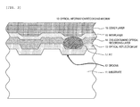
- FIG. 2 is a partly enlarged cross-sectional view showing a region B surrounded by a dashed line in FIG. 1 for explaining an internal structure according to the first embodiment.
- the optical information recording medium 10 of this embodiment has a hole at the center, and has a disc-shaped appearance with an outer diameter of approximately 120 mm, an inner diameter of approximately 15 mm, and a thickness of approximately 1.2 mm.
- the internal structure of the region B surrounded by the dashed line in FIG. 1 is schematically shown in FIG. 2 .
- a substrate 11 has an annulus ring-shaped appearance with a spiral groove 12 formed on one main surface, and has a thickness of approximately 1.1 mm and comprises a resin.
- An optical reflection layer 13 is formed on the one main surface of the substrate 11, and comprises a laser light-reflectable Ag alloy to be hereinafter described.
- a spiral groove 13b and an adjacent land 13a are formed at a track pitch TrB equal to that of the groove 12 of the substrate 11.
- An optical recording layer 14 comprising an optical absorption material capable of absorbing a laser light with a wavelength of 400 to 420 nm (e.g. 405 nm) is formed on the optical reflection layer 13.
- the optical absorption material contains an organic dye represented by the following chemical formula 1.
- the ring A represents a heterocycle containing the shown carbon atom and nitrogen atom
- the ring B represents a benzene ring that may have a substituent
- the ring C represents a heterocycle containing the shown nitrogen atom
- the ring C may be bonded to the ring B
- X - represents a group that may have an active hydrogen
- M 2+ represents a divalent positive metal ion.
- one M 2+ ion is bonded to two negative azo dye ions to form the metal complex.
- An optically transparent interlayer 15 comprising an Nb 2 O 5 -Al 2 O 3 -based composite oxide is formed on the optical recording layer 14.
- the mole ratio of Nb 2 O 5 / (Nb 2 O 5 +Al 2 O 3 ) may be 55 mol%.
- the interlayer 15 comprises the Nb 2 O 5 -Al 2 O 3 -based composite oxide, and the composite oxide has an Nb 2 O 5 content of more than 50 mol% and less than 60 mol%.
- the interlayer 15 by controlling the composition of the interlayer 15 as above, the interlayer 15 can be prevented from being scratched due to abnormal discharge between the interlayer 15 and a sputtering target.
- the interlayer 15 may be formed by an RF sputtering machine using a target having a bulk resistivity of 1 to 5 ⁇ cm. By controlling the bulk resistivity of the target, the interlayer 15 can be formed at a high film formation speed.
- an optically transparent cover layer 16 comprising a transparent resin material is formed on the interlayer 15.
- the cover layer 16 has a thickness of approximately 0.1 mm.
- the organic dye in the optical recording layer 14 absorbs the laser light and generates heat to form an optically readable pit 17 shown in FIG. 3 .
- the interlayer 15 can be readily deformed to accelerate the formation of the pit 17 in this process, whereby the optical information recording medium 10 of this embodiment can appropriately record user information.
- the substrate 11 may comprise a material selected from various known substrate materials for conventional optical information recording media.
- the materials include polycarbonates; acrylic resins such as polymethyl methacrylates; vinyl chloride based resins such as polyvinyl chlorides and vinyl chloride copolymers; epoxy resins; amorphous polyolefins; polyester resins; metals such as aluminum; and glasses.
- the materials may be used in combination if necessary.
- the thermoplastic resins are preferred, and the polycarbonates are particularly preferred, in view of formability, humidity resistance, size stability, low cost, etc.
- the above resin is preferably injection-molded to a predetermined shape to form the substrate 11.
- the substrate 11 preferably has an annulus ring shape.
- the substrate 11 preferably has a thickness of 0.9 to 1.1 mm.
- a template a so-called stamper
- the spiral groove 12 can be simultaneously formed in the injection molding.
- the groove 12 is generally formed at a pitch of 0.35 ⁇ m or 0. 32 ⁇ m.
- the substrate 11 is not limited to the embodiment, and for example the substrate 11 may be obtained by the steps of applying an ultraviolet curable resin to a base, hardening the applied resin, and removing the base.
- the optical reflection layer 13 is for reflecting a laser light for data recording and/or playback. In the invention, it is preferred that the optical reflection layer 13 is formed between the substrate 11 and the optical recording layer 14 to increase the reflectance for the laser light or to improve the recording/playback characteristic.
- the optical reflection layer 13 is preferably a metallic thin film having a high reflectance, and materials for the film include metals such as Au, Al, Ag, Cu, and Pd; alloys of the metal such as Ag alloys and Al alloys; and alloys of the metal doped with a trace constituent.
- the optical reflection layer 13 is preferably formed on the grooved surface of the substrate 11 by a deposition method, an ion plating method, a sputtering method, etc. Among the methods, the sputtering method is particularly preferred from the viewpoints of mass productivity and cost.
- the spiral groove 13b is preferably formed at a track pitch equal to that of the groove 12 of the substrate 11. It is preferred that the optical reflection layer 13 is formed with a uniform thickness by a sputtering method, etc. on the spirally grooved main surface of the substrate 11 to obtain the groove 13b.
- the optical recording layer 14 preferably comprises an optical absorption material containing an organic dye capable of absorbing a laser light.
- the optical recording layer 14 is particularly preferably such a dye type optical recording layer that a pit is formed to record data under the irradiation with the laser light.
- the organic dye is preferably a phthalocyanine dye, a cyanine dye, an azo dye, etc.
- the optical recording layer 14 is preferably formed by the steps of: dissolving an azo dye represented by the following chemical formula 1 or 2 or a cyanine dye represented by the following chemical formula 3 with a binder or the like in a solvent such as TFP (tetrafluoropropanol) to prepare a coating liquid; applying the coating liquid to the optical reflection layer on the substrate 11 using a spin coat method or a screen printing method to form a coating layer; and drying the coating layer at 80°C for 30 minutes.
- a solvent such as TFP (tetrafluoropropanol)
- the ring A represents a heterocycle containing the shown carbon atom and nitrogen atom
- the ring B represents a benzene ring that may have a substituent
- the ring C represents a heterocycle containing the shown nitrogen atom
- the ring C may be bonded to the ring B
- X - represents a group that may have an active hydrogen
- M 2+ represents a divalent positive metal ion.
- one M 2+ ion is bonded to two negative azo dye ions to form the metal complex.
- a and A' represent the same or different heterocycles containing one or more heteroatoms selected from nitrogen, oxygen, sulfur, selenium, and tellurium atoms
- R 21 to R 24 independently represent a hydrogen atom or a substituent
- Y 21 and Y 22 represent the same or different heteroatoms selected from Group 16 atoms of the periodic table.
- ⁇ + and ⁇ independently represent an indolenine ring residue, a benzoindolenine ring residue, or a dibenzoindolenine ring residue
- L represents a linking group for forming a mono- or di-carbocyanine dye
- X - represents a negative ion
- m is an integer of 0 or 1.
- the interlayer 15 is preferably formed between the optical recording layer 14 and the cover layer 16 to be hereinafter described with a purpose of preventing mixing of the optical recording layer 14 and the cover layer 16, etc.
- the interlayer 15 preferably comprises the Nb 2 O 5 -Al 2 O 3 -based composite oxide having an Nb 2 O 5 content of more than 50 mol% and less than 60 mol%.
- the interlayer 15 preferably has optical transparency, and is preferably formed on the optical recording layer 14 by a deposition method, an ion plating method, a sputtering method, etc.
- a sputtering method using an RF sputtering machine is particularly preferred from the viewpoints of mass productivity and cost.
- an alternating voltage (a high-frequency voltage) is applied between an electrically conductive vacuum chamber and a target. Electrons in the target cannot escape, and thus the electron density of the target is increased.
- the target is negatively biased, ions are drawn to and collide against the target, and the composite oxide particles are ejected from the target by the ions.
- the ejected composite oxide particles collide against and adsorb onto the optical recording layer 14 on the substrate 11 to form the interlayer 15.
- a conventional low-resistance target comprising a composite oxide with an Nb 2 O 5 content of 70 mol% in the sputtering method, abnormal discharge is often caused between the target and the deposited composite oxide interlayer.
- the composite oxide with an Nb 2 O 5 content of more than 50 mol% and less than 60 mol% has a resistance higher than that of the conventional composite oxide, whereby the abnormal discharge can be prevented between the target and the deposited interlayer 15.
- the inner pressure of the vacuum chamber is preferably 1 ⁇ 10 -2 to 1 ⁇ 10 -5 torr
- the sputtering speed is preferably 0.1 to 20 nm/sec
- the sputtering power is preferably 0.2 to 5.0 kW.
- the interlayer 15 is preferably formed by an RF sputtering machine using a target having a bulk resistivity of 1 to 5 ⁇ cm.
- the bulk resistivity of the target is preferably controlled within a range of 1 to 5 ⁇ cm by causing oxygen deficiency in the composite oxide of the target.
- the oxygen deficiency can be purposefully caused in the composite oxide by carrying out a sintering process in vacuum or reducing atmosphere in preparation of the composite oxide by burning.
- the oxygen deficiency can be purposefully caused by using all or part of a component for the composite oxide in the state of not an oxide or carbonate powder but a metal powder, and by burning the component in vacuum or oxygen-free atmosphere.
- the cover layer 16 preferably comprises an optically transparent resin, and is preferably formed by applying an ultraviolet curable resin using a spin coat method, etc.
- the cover layer 16 preferably has a thickness of 0.1 mm so that data can be recorded and/or read on the optical recording layer 14 under irradiation with a laser light with a wavelength of about 400 to 420 nm (e.g. 405 nm).
- the light transmittance of the cover layer 16, measured by a spectrophotometer using a light with a wavelength of about 400 to 420 nm (e.g. 405 nm), is preferably 70% or more, more preferably 80% or more, per 0.1 mm of a cured layer thickness.
- the cover layer 16 is not limited to the embodiment, and a sheet of an optically high-transparent resin such as a polycarbonate resin or an acrylic-based resin, having a thickness of approximately 0.1 mm, may be bonded as the cover layer 16 to the interlayer 15 using an adhesive mainly composed of a transparent ultraviolet curable resin or a transparent reactive curable resin such as an epoxy resin.
- an optically high-transparent resin such as a polycarbonate resin or an acrylic-based resin, having a thickness of approximately 0.1 mm
- optical information recording medium 10 Examples of the optical information recording medium 10 according to the embodiment of the present invention will be described below.
- a photoresist (a photosensitizer) was applied to a glass board to a predetermined thickness by a spin coat method to form a resist film.
- the resist film was exposed to a laser light from a cutting machine in a predetermined exposure width size.
- a developer was dropped onto the resultant glass board, and a developing treatment was carried out to form a convex resist pattern corresponding to a groove of a substrate for a disc-shaped optical information recording medium.
- Nickel was deposited on the glass board by a plating treatment, and the plated layer was peeled off and trimmed into a disc shape to obtain a stamper.
- the stamper was set in a cavity of an injection molding machine, and a polycarbonate resin was injected into the cavity to obtain a substrate 11 having a spiral groove 12 on one main surface.
- An Ag alloy was sputtered to a uniform thickness onto the spirally grooved main surface of the substrate 11 using a sputtering machine, to form a 100-nm-thick optical reflection layer 13 having a spiral groove 13b corresponding to the groove 12 of the substrate 11.
- the spiral groove 13b was formed on a surface of the optical reflection layer 13, opposite to the surface in contact with the grooved main surface of the substrate 11.
- a dye solution containing an organic azo dye represented by the general chemical formula 1 was applied to a thickness of 60 nm onto the resultant substrate by a spin coat method, and the applied solution was dried to form an optical recording layer 14.
- a target composed of an Nb 2 O 5 -Al 2 O 3 -based composite oxide having an Nb 2 O 5 content of 55 mol% and a bulk resistivity of 1.4 ⁇ cm was sputtered onto the resultant substrate by an RF sputtering machine at a sputtering power of 2.0 kW, to form a 25-nm-thick interlayer 15 composed of an Nb 2 O 5 -Al 2 O 3 -based composite oxide having an Nb 2 O 5 content of approximately 55 mol%.
- an ultraviolet curable resin was applied to the resultant substrate by a spin coat method, and the applied resin was hardened under UV irradiation to form a 0.1-mm-thick cover layer 16, whereby an optical information recording medium 10 was produced.
- the appearance of the produced optical information recording medium 10 was visually observed from the cover layer 16 side. As a result, a scratch or the like corresponding to abnormal discharge was not found.
- the optical information recording medium 10 was set in ODU-1000 manufactured by Pulstec Industrial Co., Ltd., an optical recording medium evaluation device equipped with a laser optical system having a wavelength of 405 nm and an NA of 0.85. On the optical information recording medium 10, 1-7 modulated random signals (2T to 8T) were recorded at a power of 5.5 mW and reproduced at a power of 0.35 mW to evaluate the electrical jitter characteristic. This process was carried out at a linear speed of 9.84 m/s using an optimized laser luminescence pattern in the recording. The optical information recording medium 10 had a jitter characteristic of 6.5%, measured by the above optical recording medium evaluation device. The film formation speed was 3.43 nm/sec, and was stable even during the discharge.
- An optical information recording medium of Example 2 was produced and evaluated in the same manner as Example 1 except that a target composed of an Nb 2 O 5 -Al 2 O 3 -based composite oxide having an Nb 2 O 5 content of 58 mol% and a bulk resistivity of 1.2 ⁇ cm was used to form an interlayer composed of an Nb 2 O 5 -Al 2 O 3 -based composite oxide having an Nb 2 O 5 content of 58 mol%.
- a scratch or the like corresponding to abnormal discharge was not found as Example 1.
- the optical information recording medium had a jitter characteristic of 6.8%.
- the film formation speed was 3.40 nm/sec, and was stable even during the discharge.
- An optical information recording medium of Example 3 was produced and evaluated in the same manner as Example 1 except that a target composed of an Nb 2 O 5 -Al 2 O 3 -based composite oxide having an Nb 2 O 5 content of 53 mol% and a bulk resistivity of 3.0 ⁇ cm was used to form an interlayer composed of an Nb 2 O 5 -Al 2 O 3 -based composite oxide having an Nb 2 O 5 content of 53 mol%.
- a scratch or the like corresponding to abnormal discharge was not found as Example 1.
- the optical information recording medium had a jitter characteristic of 6.8%.
- the film formation speed was 3.55 nm/sec, and was stable even during the discharge.
- Example 1 Ten optical information recording media of Comparative Example 1 were produced and evaluated in the same manner as Example 1 except that a target composed of an Nb 2 O 5 -Al 2 O 3 -based composite oxide having an Nb 2 O 5 content of 65 mol% and a bulk resistivity of 0. 4 ⁇ cm was used to form an interlayer composed of an Nb 2 O 5 -Al 2 O 3 -based composite oxide having an Nb 2 O 5 content of 65 mol%.
- a scratch corresponding to abnormal discharge for example having a width of 7 mm and a length of 5 mm
- the optical information recording medium had a jitter characteristic of 7.5%.
- An optical information recording medium of Comparative Example 2 was produced and evaluated in the same manner as Example 1 except that a target composed of an Nb 2 O 5 -Al 2 O 3 -based composite oxide having an Nb 2 O 5 content of 70 mol% and a bulk resistivity of 1.0E+08 ⁇ cm (an insulator) was used to form an interlayer composed of an Nb 2 O 5 -Al 2 O 3 -based composite oxide having an Nb 2 O 5 content of 70 mol%.
- the film formation speed was 0.90 nm/sec, which was remarkably lower than those of Examples.
- the optical information recording medium was not practical in view of productivity.
- An optical information recording medium of Comparative Example 3 was produced and evaluated in the same manner as Example 1 except that a target composed of an Nb 2 O 5 -Al 2 O 3 -based composite oxide having an Nb 2 O 5 content of 50 mol% and a bulk resistivity of 1.0E+08 ⁇ cm (an insulator) was used to form an interlayer composed of an Nb 2 O 5 -Al 2 O 3 -based composite oxide having an Nb 2 O 5 content of 50 mol%.
- the film formation speed was 0.80 nm/sec, which was remarkably lower than those of Examples.
- the optical information recording medium was not practical in view of productivity.
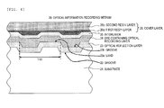
- FIG. 4 is a partly enlarged cross-sectional view showing the internal structure of an optical information recording medium 20 according to the second embodiment.
- a cover layer 26 may have a bilayer structure containing a first optically transparent resin layer 26a and a second optically transparent resin layer 26b.
- the first resin layer 26a may be an ultraviolet curable adhesive layer
- the second resin layer 26b may be a polycarbonate sheet having a thickness of less than 0.1 mm (e.g. 0.075 mm).
- the total thickness of the first resin layer 26a and the second resin layer 26b is preferably 0.1 mm.
- the optical information recording medium 20 of this embodiment is different from the optical information recording medium 10 of the first embodiment only in that the cover layer 26 has the bilayer structure containing the first optically transparent resin layer 26a and the second optically transparent resin layer 26b.
- the other components of the optical information recording medium 20 are equal to those of the first embodiment, and thus explanations therefor are omitted.
Landscapes
- Engineering & Computer Science (AREA)
- Manufacturing & Machinery (AREA)
- Manufacturing Optical Record Carriers (AREA)
- Optical Record Carriers And Manufacture Thereof (AREA)
- Thermal Transfer Or Thermal Recording In General (AREA)
Abstract
Description
- The present invention relates to an optical information recording medium, particularly to a high-recording-density optical information recording medium such as a Blu-ray disc having an optical recording layer containing an organic dye.
- Optical information recording media including optical disks have been widely used for information recording. For example, an optical information recording medium such as CD-R has a recording layer and a reflective layer formed in this order on an optically transparent resin substrate with a thickness of 1.2 mm and a diameter of 120 mm or 80 mm. In these years, there has been a demand for an optical information recording medium having a higher information recording density. Thus, use of a shorter laser wavelength (referred to as wavelength shortening) and use of an object lens having a higher numerical aperture (NA) (referred to as NA increasing) have been studied, and DVD±R and the like have been realized as such media. The DVD±R has two bonded 0.6-mm-thick optically transparent resin substrates, and has a reflective layer and a recording layer sandwiched between the substrates, so that the permissive tilt angle (tilt) value of the disc is increased by the wavelength shortening and the NA increasing.
- Recently there has been a demand for a further higher information recording density in view of recording a high-definition viewdata. Thus, an optical information recording medium having a 1.1-mm-thick resin substrate, a reflective layer and a recording layer formed on the substrate, and a 0.1-mm-thick optically transparent cover layer formed on the reflective and recording layers has been proposed. Examples of the medium include a write-once type of Blu-ray Disc (registered trademark, hereinafter referred to as BD), BD-R (BD-Rewritable). Specifically, the medium has a disc-shaped substrate having an outer diameter of 120 mm, an inner diameter of 15 mm, and a thickness of approximately 1.1 mm, and further has an optical reflection layer, a phase change recording layer, and a cover layer having a thickness of approximately 0.1 mm on the substrate. The medium is capable of recording user information on the recording layer by irradiating the cover layer side with a laser light having a wavelength of approximately 405 nm from an optical head having a numerical aperture of approximately 0.85.
- Though the recording layer of the above optical information recording medium is a phase change type layer, also a dye-containing type recording layer has been studied.
- However, the dye-containing recording layer is disadvantageous in that, for example, when a transparent resin material is applied to the recording layer to form the cover layer, the coating liquid penetrates into the dye-containing recording layer.
- In contrast, as shown in
FIG. 5 , in an optical recording medium proposed inJP-A-2003-36562 cover layer 5 are disposed on asubstrate 1 to achieve recording/playback on thecover layer 5 side, and a barrier layer 4 for preventing mixing of the recording layer 3 and thecover layer 5 is formed between the recording layer 3 and thecover layer 5. The barrier layer 4 may contain at least one selected from silicon oxide, zinc sulfide, zinc oxide, silicon nitride, silicon carbide, cerium oxide, yttrium oxide, yttrium sulfide, and mixtures of an oxide and sulfur. - However, as described in
JP-A-2003-36562 - Meanwhile, in an optical recording medium proposed in
JP-A-2006-147135 - However, the optical information recording medium proposed in
JP-A-2006-147135 - As a result of intense research, the inventors have found that, by controlling the composition of the interlayer within a predetermined range, the abnormal discharge can be prevented in the formation of the interlayer to reduce the scratch on a surface of the interlayer. Further, the inventors have found that, when the target used in the RF sputtering method is not a perfect insulator and has a resistivity controlled within a predetermined range, the interlayer can be formed at a high film formation speed.
- An object of the present invention is to provide an optical information recording medium that can be stably produced without causing an appearance failure due to scratch on a surface of an interlayer. Another object of the invention is to provide an optical information recording medium that can be easily produced by forming an interlayer at a high film formation speed.
- In view of the above object, the invention provides (1) an optical information recording medium comprising an optical reflection layer, an optical recording layer containing an organic dye, an interlayer, and a cover layer formed in this order on a substrate, wherein the interlayer comprises a sputtered Nb2O5-Al2O3-based composite oxide having an Nb2O5 content of more than 50 mol% and less than 60 mol%. Thus, a scratch is hardly generated on the interlayer due to abnormal discharge between the interlayer and a sputtering target. By controlling the Nb2O5 content of the composite oxide within the range of more than 50 mol% and less than 60 mol%, a stable target having a bulk resistivity of 1 to 5 Ω·cm can be obtained. When the Nb2O5 content of the composite oxide is 50 mol% or less or 60 mol% or more, it is difficult to obtain the stable target having a bulk resistivity of 1 to 5 Ω·cm.
- Thus, according to the invention, there is provided the optical information recording medium that can be stably produced without causing the appearance failure due to the scratch on the interlayer.
- One of the main embodiments is (2) the optical information recording medium wherein the interlayer is formed by an RF sputtering machine using a target having a bulk resistivity of 1 to 5 Ω·cm, in addition to (1). In this embodiment, the interlayer can be formed at a high film formation speed. Thus, according to the embodiment, there is provided the optical information recording medium that can be easily produced by forming the interlayer at a high film formation speed.
- The above and other objects, features, and advantages of the invention will become more apparent from the following description when taken in conjunction with the accompanying drawings.
-
-
FIG. 1 is a plan view showing the overall structure of an optical information recording medium according to a first embodiment of the present invention; -
FIG. 2 is a partly enlarged cross-sectional view showing the internal structure of a region B surrounded by a dashed line inFIG. 1 in the optical information recording medium according to the first embodiment; -
FIG. 3 is a partly enlarged cross-sectional view showing a pit formed by irradiating the optical information recording medium according to the first embodiment with a laser light; -
FIG. 4 is a partly enlarged cross-sectional view showing the internal structure of an optical information recording medium according to a second embodiment of the invention; and -
FIG. 5 is a partly enlarged cross-sectional view showing an optical information recording medium according to a background art. - A first embodiment of the optical information recording medium of the present invention will be described below with reference to
FIGS. 1 and2 .FIG. 1 is a plan view showing the overall structure of an opticalinformation recording medium 10 according to the first embodiment.FIG. 2 is a partly enlarged cross-sectional view showing a region B surrounded by a dashed line inFIG. 1 for explaining an internal structure according to the first embodiment. - As shown in
FIG. 1 , the opticalinformation recording medium 10 of this embodiment has a hole at the center, and has a disc-shaped appearance with an outer diameter of approximately 120 mm, an inner diameter of approximately 15 mm, and a thickness of approximately 1.2 mm. - In the optical
information recording medium 10, the internal structure of the region B surrounded by the dashed line inFIG. 1 is schematically shown inFIG. 2 . - As shown in
FIGS. 1 and2 , asubstrate 11 has an annulus ring-shaped appearance with aspiral groove 12 formed on one main surface, and has a thickness of approximately 1.1 mm and comprises a resin. - An
optical reflection layer 13 is formed on the one main surface of thesubstrate 11, and comprises a laser light-reflectable Ag alloy to be hereinafter described. On a surface of theoptical reflection layer 13, opposite to the surface in contact with the grooved main surface of thesubstrate 11, aspiral groove 13b and anadjacent land 13a are formed at a track pitch TrB equal to that of thegroove 12 of thesubstrate 11. - An
optical recording layer 14 comprising an optical absorption material capable of absorbing a laser light with a wavelength of 400 to 420 nm (e.g. 405 nm) is formed on theoptical reflection layer 13. For example, the optical absorption material contains an organic dye represented by the followingchemical formula 1.
- In the formula, the ring A represents a heterocycle containing the shown carbon atom and nitrogen atom, the ring B represents a benzene ring that may have a substituent, the ring C represents a heterocycle containing the shown nitrogen atom, the ring C may be bonded to the ring B, X- represents a group that may have an active hydrogen, and M2+ represents a divalent positive metal ion. Thus, one M2+ ion is bonded to two negative azo dye ions to form the metal complex.
- An optically
transparent interlayer 15 comprising an Nb2O5-Al2O3-based composite oxide is formed on theoptical recording layer 14. For example, in the composite oxide, the mole ratio of Nb2O5/ (Nb2O5+Al2O3) may be 55 mol%. Theinterlayer 15 comprises the Nb2O5-Al2O3-based composite oxide, and the composite oxide has an Nb2O5 content of more than 50 mol% and less than 60 mol%. In the formation of theinterlayer 15, by controlling the composition of theinterlayer 15 as above, theinterlayer 15 can be prevented from being scratched due to abnormal discharge between theinterlayer 15 and a sputtering target. Theinterlayer 15 may be formed by an RF sputtering machine using a target having a bulk resistivity of 1 to 5 Ω·cm. By controlling the bulk resistivity of the target, theinterlayer 15 can be formed at a high film formation speed. - Further, an optically
transparent cover layer 16 comprising a transparent resin material is formed on theinterlayer 15. Thecover layer 16 has a thickness of approximately 0.1 mm. - When the optically
transparent cover layer 16 side of the opticalinformation recording medium 10 of this embodiment is irradiated with a laser light with a wavelength of 400 to 420 nm (e.g. 405 nm), the organic dye in theoptical recording layer 14 absorbs the laser light and generates heat to form an opticallyreadable pit 17 shown inFIG. 3 . Theinterlayer 15 can be readily deformed to accelerate the formation of thepit 17 in this process, whereby the opticalinformation recording medium 10 of this embodiment can appropriately record user information. - A preferred embodiment of the
substrate 11 will be described below. Thesubstrate 11 may comprise a material selected from various known substrate materials for conventional optical information recording media. Specific examples of the materials include polycarbonates; acrylic resins such as polymethyl methacrylates; vinyl chloride based resins such as polyvinyl chlorides and vinyl chloride copolymers; epoxy resins; amorphous polyolefins; polyester resins; metals such as aluminum; and glasses. The materials may be used in combination if necessary. Among the materials, the thermoplastic resins are preferred, and the polycarbonates are particularly preferred, in view of formability, humidity resistance, size stability, low cost, etc. - The above resin is preferably injection-molded to a predetermined shape to form the
substrate 11. In the case of producing an optical disk, thesubstrate 11 preferably has an annulus ring shape. Thesubstrate 11 preferably has a thickness of 0.9 to 1.1 mm. In the injection molding for forming thesubstrate 11, it is preferred that a template (a so-called stamper) is placed in a metal mold, a spiral convex portion having a reverse pattern to thegroove 12 being microfabricated on one main surface of the template. By using the template, thespiral groove 12 can be simultaneously formed in the injection molding. Thegroove 12 is generally formed at a pitch of 0.35 µm or 0. 32 µm. Thesubstrate 11 is not limited to the embodiment, and for example thesubstrate 11 may be obtained by the steps of applying an ultraviolet curable resin to a base, hardening the applied resin, and removing the base. - A preferred embodiment of the
optical reflection layer 13 will be described below. Theoptical reflection layer 13 is for reflecting a laser light for data recording and/or playback. In the invention, it is preferred that theoptical reflection layer 13 is formed between thesubstrate 11 and theoptical recording layer 14 to increase the reflectance for the laser light or to improve the recording/playback characteristic. Theoptical reflection layer 13 is preferably a metallic thin film having a high reflectance, and materials for the film include metals such as Au, Al, Ag, Cu, and Pd; alloys of the metal such as Ag alloys and Al alloys; and alloys of the metal doped with a trace constituent. Theoptical reflection layer 13 is preferably formed on the grooved surface of thesubstrate 11 by a deposition method, an ion plating method, a sputtering method, etc. Among the methods, the sputtering method is particularly preferred from the viewpoints of mass productivity and cost. On a surface of theoptical reflection layer 13, opposite to the surface in contact with the grooved main surface of thesubstrate 11, thespiral groove 13b is preferably formed at a track pitch equal to that of thegroove 12 of thesubstrate 11. It is preferred that theoptical reflection layer 13 is formed with a uniform thickness by a sputtering method, etc. on the spirally grooved main surface of thesubstrate 11 to obtain thegroove 13b. - A preferred embodiment of the
optical recording layer 14 will be described below. Theoptical recording layer 14 preferably comprises an optical absorption material containing an organic dye capable of absorbing a laser light. Theoptical recording layer 14 is particularly preferably such a dye type optical recording layer that a pit is formed to record data under the irradiation with the laser light. The organic dye is preferably a phthalocyanine dye, a cyanine dye, an azo dye, etc. For example, theoptical recording layer 14 is preferably formed by the steps of: dissolving an azo dye represented by the followingchemical formula 1 or 2 or a cyanine dye represented by the following chemical formula 3 with a binder or the like in a solvent such as TFP (tetrafluoropropanol) to prepare a coating liquid; applying the coating liquid to the optical reflection layer on thesubstrate 11 using a spin coat method or a screen printing method to form a coating layer; and drying the coating layer at 80°C for 30 minutes.
- In the formula, the ring A represents a heterocycle containing the shown carbon atom and nitrogen atom, the ring B represents a benzene ring that may have a substituent, the ring C represents a heterocycle containing the shown nitrogen atom, the ring C may be bonded to the ring B, X- represents a group that may have an active hydrogen, and M2+ represents a divalent positive metal ion. Thus, one M2+ ion is bonded to two negative azo dye ions to form the metal complex.
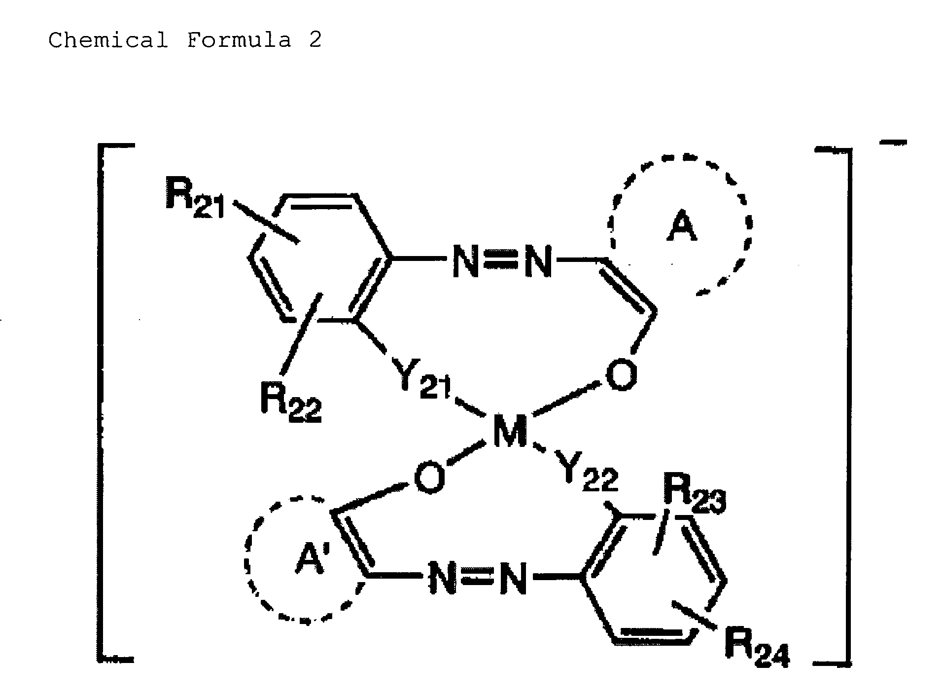
- In the formula, A and A' represent the same or different heterocycles containing one or more heteroatoms selected from nitrogen, oxygen, sulfur, selenium, and tellurium atoms, R21 to R24 independently represent a hydrogen atom or a substituent, and Y21 and Y22 represent the same or different heteroatoms selected from
Group 16 atoms of the periodic table.

- In the formula, Φ+ and φ independently represent an indolenine ring residue, a benzoindolenine ring residue, or a dibenzoindolenine ring residue, L represents a linking group for forming a mono- or di-carbocyanine dye, X- represents a negative ion, and m is an integer of 0 or 1.
- A preferred embodiment of the
interlayer 15 will be described below. Theinterlayer 15 is preferably formed between theoptical recording layer 14 and thecover layer 16 to be hereinafter described with a purpose of preventing mixing of theoptical recording layer 14 and thecover layer 16, etc. - The
interlayer 15 preferably comprises the Nb2O5-Al2O3-based composite oxide having an Nb2O5 content of more than 50 mol% and less than 60 mol%. Theinterlayer 15 preferably has optical transparency, and is preferably formed on theoptical recording layer 14 by a deposition method, an ion plating method, a sputtering method, etc. Among the methods, a sputtering method using an RF sputtering machine is particularly preferred from the viewpoints of mass productivity and cost. In the RF sputtering machine, an alternating voltage (a high-frequency voltage) is applied between an electrically conductive vacuum chamber and a target. Electrons in the target cannot escape, and thus the electron density of the target is increased. As a result, the target is negatively biased, ions are drawn to and collide against the target, and the composite oxide particles are ejected from the target by the ions. The ejected composite oxide particles collide against and adsorb onto theoptical recording layer 14 on thesubstrate 11 to form theinterlayer 15. In the case of using a conventional low-resistance target comprising a composite oxide with an Nb2O5 content of 70 mol% in the sputtering method, abnormal discharge is often caused between the target and the deposited composite oxide interlayer. In the invention, the composite oxide with an Nb2O5 content of more than 50 mol% and less than 60 mol% has a resistance higher than that of the conventional composite oxide, whereby the abnormal discharge can be prevented between the target and the depositedinterlayer 15. In the sputtering method for forming theinterlayer 15 by the RF sputtering machine, the inner pressure of the vacuum chamber is preferably 1×10⁻² to 1×10⁻⁵ torr, the sputtering speed is preferably 0.1 to 20 nm/sec, and the sputtering power is preferably 0.2 to 5.0 kW. - The
interlayer 15 is preferably formed by an RF sputtering machine using a target having a bulk resistivity of 1 to 5 Ω·cm. - For example, the bulk resistivity of the target is preferably controlled within a range of 1 to 5 Ω·cm by causing oxygen deficiency in the composite oxide of the target.
- For example, the oxygen deficiency can be purposefully caused in the composite oxide by carrying out a sintering process in vacuum or reducing atmosphere in preparation of the composite oxide by burning.
- Further, the oxygen deficiency can be purposefully caused by using all or part of a component for the composite oxide in the state of not an oxide or carbonate powder but a metal powder, and by burning the component in vacuum or oxygen-free atmosphere.
- A preferred embodiment of the
cover layer 16 will be described below. Thecover layer 16 preferably comprises an optically transparent resin, and is preferably formed by applying an ultraviolet curable resin using a spin coat method, etc. Thecover layer 16 preferably has a thickness of 0.1 mm so that data can be recorded and/or read on theoptical recording layer 14 under irradiation with a laser light with a wavelength of about 400 to 420 nm (e.g. 405 nm). The light transmittance of thecover layer 16, measured by a spectrophotometer using a light with a wavelength of about 400 to 420 nm (e.g. 405 nm), is preferably 70% or more, more preferably 80% or more, per 0.1 mm of a cured layer thickness. Thecover layer 16 is not limited to the embodiment, and a sheet of an optically high-transparent resin such as a polycarbonate resin or an acrylic-based resin, having a thickness of approximately 0.1 mm, may be bonded as thecover layer 16 to theinterlayer 15 using an adhesive mainly composed of a transparent ultraviolet curable resin or a transparent reactive curable resin such as an epoxy resin. - Examples of the optical
information recording medium 10 according to the embodiment of the present invention will be described below. - A photoresist (a photosensitizer) was applied to a glass board to a predetermined thickness by a spin coat method to form a resist film. The resist film was exposed to a laser light from a cutting machine in a predetermined exposure width size. A developer was dropped onto the resultant glass board, and a developing treatment was carried out to form a convex resist pattern corresponding to a groove of a substrate for a disc-shaped optical information recording medium.
- Nickel was deposited on the glass board by a plating treatment, and the plated layer was peeled off and trimmed into a disc shape to obtain a stamper.
- The stamper was set in a cavity of an injection molding machine, and a polycarbonate resin was injected into the cavity to obtain a
substrate 11 having aspiral groove 12 on one main surface. - An Ag alloy was sputtered to a uniform thickness onto the spirally grooved main surface of the
substrate 11 using a sputtering machine, to form a 100-nm-thickoptical reflection layer 13 having aspiral groove 13b corresponding to thegroove 12 of thesubstrate 11. Thespiral groove 13b was formed on a surface of theoptical reflection layer 13, opposite to the surface in contact with the grooved main surface of thesubstrate 11. - A dye solution containing an organic azo dye represented by the
general chemical formula 1 was applied to a thickness of 60 nm onto the resultant substrate by a spin coat method, and the applied solution was dried to form anoptical recording layer 14. - A target composed of an Nb2O5-Al2O3-based composite oxide having an Nb2O5 content of 55 mol% and a bulk resistivity of 1.4 Ω·cm was sputtered onto the resultant substrate by an RF sputtering machine at a sputtering power of 2.0 kW, to form a 25-nm-
thick interlayer 15 composed of an Nb2O5-Al2O3-based composite oxide having an Nb2O5 content of approximately 55 mol%. - Then, an ultraviolet curable resin was applied to the resultant substrate by a spin coat method, and the applied resin was hardened under UV irradiation to form a 0.1-mm-
thick cover layer 16, whereby an opticalinformation recording medium 10 was produced. - The appearance of the produced optical
information recording medium 10 was visually observed from thecover layer 16 side. As a result, a scratch or the like corresponding to abnormal discharge was not found. The opticalinformation recording medium 10 was set in ODU-1000 manufactured by Pulstec Industrial Co., Ltd., an optical recording medium evaluation device equipped with a laser optical system having a wavelength of 405 nm and an NA of 0.85. On the opticalinformation recording medium 10, 1-7 modulated random signals (2T to 8T) were recorded at a power of 5.5 mW and reproduced at a power of 0.35 mW to evaluate the electrical jitter characteristic. This process was carried out at a linear speed of 9.84 m/s using an optimized laser luminescence pattern in the recording. The opticalinformation recording medium 10 had a jitter characteristic of 6.5%, measured by the above optical recording medium evaluation device. The film formation speed was 3.43 nm/sec, and was stable even during the discharge. - An optical information recording medium of Example 2 was produced and evaluated in the same manner as Example 1 except that a target composed of an Nb2O5-Al2O3-based composite oxide having an Nb2O5 content of 58 mol% and a bulk resistivity of 1.2 Ω·cm was used to form an interlayer composed of an Nb2O5-Al2O3-based composite oxide having an Nb2O5 content of 58 mol%. As a result of observing the appearance of the optical information recording medium, a scratch or the like corresponding to abnormal discharge was not found as Example 1. The optical information recording medium had a jitter characteristic of 6.8%. The film formation speed was 3.40 nm/sec, and was stable even during the discharge.
- An optical information recording medium of Example 3 was produced and evaluated in the same manner as Example 1 except that a target composed of an Nb2O5-Al2O3-based composite oxide having an Nb2O5 content of 53 mol% and a bulk resistivity of 3.0 Ω·cm was used to form an interlayer composed of an Nb2O5-Al2O3-based composite oxide having an Nb2O5 content of 53 mol%. As a result of observing the appearance of the optical information recording medium, a scratch or the like corresponding to abnormal discharge was not found as Example 1. The optical information recording medium had a jitter characteristic of 6.8%. The film formation speed was 3.55 nm/sec, and was stable even during the discharge.
- Ten optical information recording media of Comparative Example 1 were produced and evaluated in the same manner as Example 1 except that a target composed of an Nb2O5-Al2O3-based composite oxide having an Nb2O5 content of 65 mol% and a bulk resistivity of 0. 4 Ω·cm was used to form an interlayer composed of an Nb2O5-Al2O3-based composite oxide having an Nb2O5 content of 65 mol%. As a result of observing the appearance of the optical information recording media, a scratch corresponding to abnormal discharge (for example having a width of 7 mm and a length of 5 mm) was found in all the ten media. The optical information recording medium had a jitter characteristic of 7.5%.
- An optical information recording medium of Comparative Example 2 was produced and evaluated in the same manner as Example 1 except that a target composed of an Nb2O5-Al2O3-based composite oxide having an Nb2O5 content of 70 mol% and a bulk resistivity of 1.0E+08 Ω·cm (an insulator) was used to form an interlayer composed of an Nb2O5-Al2O3-based composite oxide having an Nb2O5 content of 70 mol%. As a result, the film formation speed was 0.90 nm/sec, which was remarkably lower than those of Examples. Thus, the optical information recording medium was not practical in view of productivity.
- An optical information recording medium of Comparative Example 3 was produced and evaluated in the same manner as Example 1 except that a target composed of an Nb2O5-Al2O3-based composite oxide having an Nb2O5 content of 50 mol% and a bulk resistivity of 1.0E+08 Ω·cm (an insulator) was used to form an interlayer composed of an Nb2O5-Al2O3-based composite oxide having an Nb2O5 content of 50 mol%. As a result, the film formation speed was 0.80 nm/sec, which was remarkably lower than those of Examples. Thus, the optical information recording medium was not practical in view of productivity.
- A second embodiment of the optical information recording medium of the invention will be described below with reference to
FIG. 4. FIG. 4 is a partly enlarged cross-sectional view showing the internal structure of an opticalinformation recording medium 20 according to the second embodiment. - Though the
cover layer 16 has a single-layer structure in the opticalinformation recording medium 10 of the above first embodiment, the cover layer used in the invention is not limited thereto. For example, as shown inFIG. 4 , acover layer 26 may have a bilayer structure containing a first opticallytransparent resin layer 26a and a second opticallytransparent resin layer 26b. Thefirst resin layer 26a may be an ultraviolet curable adhesive layer, and thesecond resin layer 26b may be a polycarbonate sheet having a thickness of less than 0.1 mm (e.g. 0.075 mm). In this case, the total thickness of thefirst resin layer 26a and thesecond resin layer 26b is preferably 0.1 mm. - The optical
information recording medium 20 of this embodiment is different from the opticalinformation recording medium 10 of the first embodiment only in that thecover layer 26 has the bilayer structure containing the first opticallytransparent resin layer 26a and the second opticallytransparent resin layer 26b. The other components of the opticalinformation recording medium 20 are equal to those of the first embodiment, and thus explanations therefor are omitted.
Claims (2)
- An optical information recording medium comprising an optical reflection layer, an optical recording layer containing an organic dye, an interlayer, and a cover layer formed in this order on a substrate, wherein the interlayer comprises a sputtered Nb2O5-Al2O3-based composite oxide having an Nb2O5 content of more than 50 mol% and less than 60 mol%.
- An optical information recording medium according to claim 1, wherein the interlayer is formed by an RF sputtering machine using a target having a bulk resistivity of 1 to 5 Ω·cm.
Applications Claiming Priority (1)
| Application Number | Priority Date | Filing Date | Title |
|---|---|---|---|
| JP2007261468A JP4695632B2 (en) | 2007-10-05 | 2007-10-05 | Optical information recording medium |
Publications (2)
| Publication Number | Publication Date |
|---|---|
| EP2053605A1 true EP2053605A1 (en) | 2009-04-29 |
| EP2053605B1 EP2053605B1 (en) | 2013-04-24 |
Family
ID=40433900
Family Applications (1)
| Application Number | Title | Priority Date | Filing Date |
|---|---|---|---|
| EP08253207.8A Not-in-force EP2053605B1 (en) | 2007-10-05 | 2008-10-02 | Optical information recording medium |
Country Status (5)
| Country | Link |
|---|---|
| US (1) | US8025947B2 (en) |
| EP (1) | EP2053605B1 (en) |
| JP (1) | JP4695632B2 (en) |
| CN (1) | CN101414469B (en) |
| TW (1) | TW200917244A (en) |
Families Citing this family (1)
| Publication number | Priority date | Publication date | Assignee | Title |
|---|---|---|---|---|
| US7596077B2 (en) * | 2002-08-30 | 2009-09-29 | Sony Corporation | Optical disk |
Citations (3)
| Publication number | Priority date | Publication date | Assignee | Title |
|---|---|---|---|---|
| JP2003036562A (en) | 2001-07-23 | 2003-02-07 | Mitsubishi Chemicals Corp | Optical recording medium |
| JP2006147135A (en) | 2004-10-20 | 2006-06-08 | Fuji Photo Film Co Ltd | Optical recording medium |
| US20070231529A1 (en) * | 2006-03-23 | 2007-10-04 | Nec Corporation | Optical information recording medium suppressing sulfuration of silver |
Family Cites Families (5)
| Publication number | Priority date | Publication date | Assignee | Title |
|---|---|---|---|---|
| JP2004244722A (en) * | 2003-01-24 | 2004-09-02 | Olympus Corp | Thin film deposition apparatus, thin film deposition method, and optical element |
| CN101076859A (en) * | 2004-10-18 | 2007-11-21 | 富士胶片株式会社 | Optical information recording medium and manufacturing method thereof |
| JPWO2006043357A1 (en) * | 2004-10-18 | 2008-05-22 | 松下電器産業株式会社 | Optical information recording medium and manufacturing method thereof |
| JP2007035081A (en) * | 2005-07-22 | 2007-02-08 | Taiyo Yuden Co Ltd | Optical information recording medium |
| JP2009080871A (en) * | 2007-09-25 | 2009-04-16 | Taiyo Yuden Co Ltd | Optical information recording medium |
-
2007
- 2007-10-05 JP JP2007261468A patent/JP4695632B2/en not_active Expired - Fee Related
-
2008
- 2008-09-23 TW TW097136492A patent/TW200917244A/en unknown
- 2008-09-26 CN CN200810211464.1A patent/CN101414469B/en not_active Expired - Fee Related
- 2008-10-01 US US12/243,922 patent/US8025947B2/en not_active Expired - Fee Related
- 2008-10-02 EP EP08253207.8A patent/EP2053605B1/en not_active Not-in-force
Patent Citations (3)
| Publication number | Priority date | Publication date | Assignee | Title |
|---|---|---|---|---|
| JP2003036562A (en) | 2001-07-23 | 2003-02-07 | Mitsubishi Chemicals Corp | Optical recording medium |
| JP2006147135A (en) | 2004-10-20 | 2006-06-08 | Fuji Photo Film Co Ltd | Optical recording medium |
| US20070231529A1 (en) * | 2006-03-23 | 2007-10-04 | Nec Corporation | Optical information recording medium suppressing sulfuration of silver |
Non-Patent Citations (1)
| Title |
|---|
| Retrieved from the Internet <URL:http://dossier1.ipdl.inpit.go.jp/AIPN/aipn_call_transl.ipdl?N0000=7413&N0120=01&N2001=2&N3001=2006-147135> [retrieved on 20090319] * |
Also Published As
| Publication number | Publication date |
|---|---|
| CN101414469A (en) | 2009-04-22 |
| US20090092783A1 (en) | 2009-04-09 |
| EP2053605B1 (en) | 2013-04-24 |
| TW200917244A (en) | 2009-04-16 |
| JP4695632B2 (en) | 2011-06-08 |
| JP2009093725A (en) | 2009-04-30 |
| US8025947B2 (en) | 2011-09-27 |
| CN101414469B (en) | 2011-04-06 |
| HK1129943A1 (en) | 2009-12-11 |
Similar Documents
| Publication | Publication Date | Title |
|---|---|---|
| CN1336654A (en) | Metal alloys for reflective or semi-reflective layers of optical storage media | |
| JP4996607B2 (en) | Information recording medium, manufacturing method thereof, and sputtering target | |
| WO2017159560A1 (en) | Information recording medium, and method for producing information recording medium | |
| WO2016129237A1 (en) | Information recording medium and method for manufacturing information recording medium | |
| EP2216780B1 (en) | Recordable optical recording medium and method for manufacturing the same | |
| CN103050136B (en) | Recording layer for optic informating recording medium and optic informating recording medium | |
| CN110313032A (en) | Information recording carrier and its manufacturing method and sputtering target | |
| EP2054889A1 (en) | Recordable optical recording medium and recording method thereof | |
| US8470428B2 (en) | Optical recording medium | |
| EP2053605B1 (en) | Optical information recording medium | |
| JP2003303447A (en) | Optical recording medium | |
| JP2011253577A (en) | Optical recording medium and manufacturing method thereof | |
| EP2045805A1 (en) | Optical information recording medium | |
| US8394480B2 (en) | Optical information recording medium and manufacturing method therefor | |
| JP4755680B2 (en) | Optical information recording medium and manufacturing method thereof | |
| HK1129943B (en) | Optical information recording medium | |
| JP4322719B2 (en) | Optical information recording medium, method for producing the same, and sputtering target | |
| JP3600177B2 (en) | Optical recording medium and manufacturing method thereof | |
| CN116417018A (en) | Information recording medium and manufacturing method thereof | |
| US20070014963A1 (en) | Metal alloys for the reflective layer of an optical storage medium | |
| HK1132082B (en) | Optical information recording medium and a manufacturing method thereof | |
| EP2071569A1 (en) | Optical information recording media and method for producing the same | |
| JP2007149306A (en) | Optical recording medium and manufacturing method of the same | |
| CN101025963A (en) | Optical recording medium, method for producing recording layer thereof, and recording method thereof |
Legal Events
| Date | Code | Title | Description |
|---|---|---|---|
| PUAI | Public reference made under article 153(3) epc to a published international application that has entered the european phase |
Free format text: ORIGINAL CODE: 0009012 |
|
| AK | Designated contracting states |
Kind code of ref document: A1 Designated state(s): AT BE BG CH CY CZ DE DK EE ES FI FR GB GR HR HU IE IS IT LI LT LU LV MC MT NL NO PL PT RO SE SI SK TR |
|
| AX | Request for extension of the european patent |
Extension state: AL BA MK RS |
|
| 17P | Request for examination filed |
Effective date: 20091007 |
|
| 17Q | First examination report despatched |
Effective date: 20091105 |
|
| AKX | Designation fees paid |
Designated state(s): AT BE BG CH CY CZ DE DK EE ES FI FR GB GR HR HU IE IS IT LI LT LU LV MC MT NL NO PL PT RO SE SI SK TR |
|
| REG | Reference to a national code |
Ref country code: DE Ref legal event code: R079 Ref document number: 602008024039 Country of ref document: DE Free format text: PREVIOUS MAIN CLASS: G11B0007257000 Ipc: G11B0007260000 |
|
| GRAP | Despatch of communication of intention to grant a patent |
Free format text: ORIGINAL CODE: EPIDOSNIGR1 |
|
| RIC1 | Information provided on ipc code assigned before grant |
Ipc: G11B 7/26 20060101AFI20120904BHEP |
|
| GRAS | Grant fee paid |
Free format text: ORIGINAL CODE: EPIDOSNIGR3 |
|
| GRAA | (expected) grant |
Free format text: ORIGINAL CODE: 0009210 |
|
| AK | Designated contracting states |
Kind code of ref document: B1 Designated state(s): AT BE BG CH CY CZ DE DK EE ES FI FR GB GR HR HU IE IS IT LI LT LU LV MC MT NL NO PL PT RO SE SI SK TR |
|
| REG | Reference to a national code |
Ref country code: GB Ref legal event code: FG4D |
|
| REG | Reference to a national code |
Ref country code: CH Ref legal event code: EP |
|
| REG | Reference to a national code |
Ref country code: AT Ref legal event code: REF Ref document number: 609040 Country of ref document: AT Kind code of ref document: T Effective date: 20130515 |
|
| REG | Reference to a national code |
Ref country code: IE Ref legal event code: FG4D |
|
| REG | Reference to a national code |
Ref country code: DE Ref legal event code: R096 Ref document number: 602008024039 Country of ref document: DE Effective date: 20130620 |
|
| REG | Reference to a national code |
Ref country code: AT Ref legal event code: MK05 Ref document number: 609040 Country of ref document: AT Kind code of ref document: T Effective date: 20130424 |
|
| REG | Reference to a national code |
Ref country code: LT Ref legal event code: MG4D |
|
| REG | Reference to a national code |
Ref country code: NL Ref legal event code: VDEP Effective date: 20130424 |
|
| PG25 | Lapsed in a contracting state [announced via postgrant information from national office to epo] |
Ref country code: IS Free format text: LAPSE BECAUSE OF FAILURE TO SUBMIT A TRANSLATION OF THE DESCRIPTION OR TO PAY THE FEE WITHIN THE PRESCRIBED TIME-LIMIT Effective date: 20130824 Ref country code: PT Free format text: LAPSE BECAUSE OF FAILURE TO SUBMIT A TRANSLATION OF THE DESCRIPTION OR TO PAY THE FEE WITHIN THE PRESCRIBED TIME-LIMIT Effective date: 20130826 Ref country code: AT Free format text: LAPSE BECAUSE OF FAILURE TO SUBMIT A TRANSLATION OF THE DESCRIPTION OR TO PAY THE FEE WITHIN THE PRESCRIBED TIME-LIMIT Effective date: 20130424 Ref country code: BE Free format text: LAPSE BECAUSE OF FAILURE TO SUBMIT A TRANSLATION OF THE DESCRIPTION OR TO PAY THE FEE WITHIN THE PRESCRIBED TIME-LIMIT Effective date: 20130424 Ref country code: GR Free format text: LAPSE BECAUSE OF FAILURE TO SUBMIT A TRANSLATION OF THE DESCRIPTION OR TO PAY THE FEE WITHIN THE PRESCRIBED TIME-LIMIT Effective date: 20130725 Ref country code: SI Free format text: LAPSE BECAUSE OF FAILURE TO SUBMIT A TRANSLATION OF THE DESCRIPTION OR TO PAY THE FEE WITHIN THE PRESCRIBED TIME-LIMIT Effective date: 20130424 Ref country code: SE Free format text: LAPSE BECAUSE OF FAILURE TO SUBMIT A TRANSLATION OF THE DESCRIPTION OR TO PAY THE FEE WITHIN THE PRESCRIBED TIME-LIMIT Effective date: 20130424 Ref country code: ES Free format text: LAPSE BECAUSE OF FAILURE TO SUBMIT A TRANSLATION OF THE DESCRIPTION OR TO PAY THE FEE WITHIN THE PRESCRIBED TIME-LIMIT Effective date: 20130804 Ref country code: LT Free format text: LAPSE BECAUSE OF FAILURE TO SUBMIT A TRANSLATION OF THE DESCRIPTION OR TO PAY THE FEE WITHIN THE PRESCRIBED TIME-LIMIT Effective date: 20130424 Ref country code: NO Free format text: LAPSE BECAUSE OF FAILURE TO SUBMIT A TRANSLATION OF THE DESCRIPTION OR TO PAY THE FEE WITHIN THE PRESCRIBED TIME-LIMIT Effective date: 20130724 Ref country code: FI Free format text: LAPSE BECAUSE OF FAILURE TO SUBMIT A TRANSLATION OF THE DESCRIPTION OR TO PAY THE FEE WITHIN THE PRESCRIBED TIME-LIMIT Effective date: 20130424 |
|
| PG25 | Lapsed in a contracting state [announced via postgrant information from national office to epo] |
Ref country code: LV Free format text: LAPSE BECAUSE OF FAILURE TO SUBMIT A TRANSLATION OF THE DESCRIPTION OR TO PAY THE FEE WITHIN THE PRESCRIBED TIME-LIMIT Effective date: 20130424 Ref country code: BG Free format text: LAPSE BECAUSE OF FAILURE TO SUBMIT A TRANSLATION OF THE DESCRIPTION OR TO PAY THE FEE WITHIN THE PRESCRIBED TIME-LIMIT Effective date: 20130724 Ref country code: PL Free format text: LAPSE BECAUSE OF FAILURE TO SUBMIT A TRANSLATION OF THE DESCRIPTION OR TO PAY THE FEE WITHIN THE PRESCRIBED TIME-LIMIT Effective date: 20130424 Ref country code: HR Free format text: LAPSE BECAUSE OF FAILURE TO SUBMIT A TRANSLATION OF THE DESCRIPTION OR TO PAY THE FEE WITHIN THE PRESCRIBED TIME-LIMIT Effective date: 20130424 Ref country code: CY Free format text: LAPSE BECAUSE OF FAILURE TO SUBMIT A TRANSLATION OF THE DESCRIPTION OR TO PAY THE FEE WITHIN THE PRESCRIBED TIME-LIMIT Effective date: 20130424 |
|
| PG25 | Lapsed in a contracting state [announced via postgrant information from national office to epo] |
Ref country code: SK Free format text: LAPSE BECAUSE OF FAILURE TO SUBMIT A TRANSLATION OF THE DESCRIPTION OR TO PAY THE FEE WITHIN THE PRESCRIBED TIME-LIMIT Effective date: 20130424 Ref country code: CZ Free format text: LAPSE BECAUSE OF FAILURE TO SUBMIT A TRANSLATION OF THE DESCRIPTION OR TO PAY THE FEE WITHIN THE PRESCRIBED TIME-LIMIT Effective date: 20130424 Ref country code: DK Free format text: LAPSE BECAUSE OF FAILURE TO SUBMIT A TRANSLATION OF THE DESCRIPTION OR TO PAY THE FEE WITHIN THE PRESCRIBED TIME-LIMIT Effective date: 20130424 Ref country code: EE Free format text: LAPSE BECAUSE OF FAILURE TO SUBMIT A TRANSLATION OF THE DESCRIPTION OR TO PAY THE FEE WITHIN THE PRESCRIBED TIME-LIMIT Effective date: 20130424 |
|
| PG25 | Lapsed in a contracting state [announced via postgrant information from national office to epo] |
Ref country code: NL Free format text: LAPSE BECAUSE OF FAILURE TO SUBMIT A TRANSLATION OF THE DESCRIPTION OR TO PAY THE FEE WITHIN THE PRESCRIBED TIME-LIMIT Effective date: 20130424 Ref country code: IT Free format text: LAPSE BECAUSE OF FAILURE TO SUBMIT A TRANSLATION OF THE DESCRIPTION OR TO PAY THE FEE WITHIN THE PRESCRIBED TIME-LIMIT Effective date: 20130424 Ref country code: RO Free format text: LAPSE BECAUSE OF FAILURE TO SUBMIT A TRANSLATION OF THE DESCRIPTION OR TO PAY THE FEE WITHIN THE PRESCRIBED TIME-LIMIT Effective date: 20130424 |
|
| PLBE | No opposition filed within time limit |
Free format text: ORIGINAL CODE: 0009261 |
|
| STAA | Information on the status of an ep patent application or granted ep patent |
Free format text: STATUS: NO OPPOSITION FILED WITHIN TIME LIMIT |
|
| 26N | No opposition filed |
Effective date: 20140127 |
|
| REG | Reference to a national code |
Ref country code: DE Ref legal event code: R097 Ref document number: 602008024039 Country of ref document: DE Effective date: 20140127 |
|
| PG25 | Lapsed in a contracting state [announced via postgrant information from national office to epo] |
Ref country code: MC Free format text: LAPSE BECAUSE OF FAILURE TO SUBMIT A TRANSLATION OF THE DESCRIPTION OR TO PAY THE FEE WITHIN THE PRESCRIBED TIME-LIMIT Effective date: 20130424 |
|
| REG | Reference to a national code |
Ref country code: CH Ref legal event code: PL |
|
| GBPC | Gb: european patent ceased through non-payment of renewal fee |
Effective date: 20131002 |
|
| REG | Reference to a national code |
Ref country code: IE Ref legal event code: MM4A |
|
| PG25 | Lapsed in a contracting state [announced via postgrant information from national office to epo] |
Ref country code: GB Free format text: LAPSE BECAUSE OF NON-PAYMENT OF DUE FEES Effective date: 20131002 Ref country code: CH Free format text: LAPSE BECAUSE OF NON-PAYMENT OF DUE FEES Effective date: 20131031 Ref country code: LI Free format text: LAPSE BECAUSE OF NON-PAYMENT OF DUE FEES Effective date: 20131031 |
|
| REG | Reference to a national code |
Ref country code: FR Ref legal event code: ST Effective date: 20140630 |
|
| REG | Reference to a national code |
Ref country code: DE Ref legal event code: R119 Ref document number: 602008024039 Country of ref document: DE Effective date: 20140501 |
|
| PG25 | Lapsed in a contracting state [announced via postgrant information from national office to epo] |
Ref country code: DE Free format text: LAPSE BECAUSE OF NON-PAYMENT OF DUE FEES Effective date: 20140501 Ref country code: FR Free format text: LAPSE BECAUSE OF NON-PAYMENT OF DUE FEES Effective date: 20131031 |
|
| PG25 | Lapsed in a contracting state [announced via postgrant information from national office to epo] |
Ref country code: IE Free format text: LAPSE BECAUSE OF NON-PAYMENT OF DUE FEES Effective date: 20131002 |
|
| PG25 | Lapsed in a contracting state [announced via postgrant information from national office to epo] |
Ref country code: TR Free format text: LAPSE BECAUSE OF FAILURE TO SUBMIT A TRANSLATION OF THE DESCRIPTION OR TO PAY THE FEE WITHIN THE PRESCRIBED TIME-LIMIT Effective date: 20130424 |
|
| PG25 | Lapsed in a contracting state [announced via postgrant information from national office to epo] |
Ref country code: LU Free format text: LAPSE BECAUSE OF NON-PAYMENT OF DUE FEES Effective date: 20131002 Ref country code: HU Free format text: LAPSE BECAUSE OF FAILURE TO SUBMIT A TRANSLATION OF THE DESCRIPTION OR TO PAY THE FEE WITHIN THE PRESCRIBED TIME-LIMIT; INVALID AB INITIO Effective date: 20081002 |
|
| PG25 | Lapsed in a contracting state [announced via postgrant information from national office to epo] |
Ref country code: MT Free format text: LAPSE BECAUSE OF FAILURE TO SUBMIT A TRANSLATION OF THE DESCRIPTION OR TO PAY THE FEE WITHIN THE PRESCRIBED TIME-LIMIT Effective date: 20130424 |