EP2048687A2 - Protective layer, method of manufacturing the same, and plasma display panel including the same - Google Patents
Protective layer, method of manufacturing the same, and plasma display panel including the same Download PDFInfo
- Publication number
- EP2048687A2 EP2048687A2 EP08253276A EP08253276A EP2048687A2 EP 2048687 A2 EP2048687 A2 EP 2048687A2 EP 08253276 A EP08253276 A EP 08253276A EP 08253276 A EP08253276 A EP 08253276A EP 2048687 A2 EP2048687 A2 EP 2048687A2
- Authority
- EP
- European Patent Office
- Prior art keywords
- protective layer
- impurity
- magnesium oxide
- pellets
- pdp
- Prior art date
- Legal status (The legal status is an assumption and is not a legal conclusion. Google has not performed a legal analysis and makes no representation as to the accuracy of the status listed.)
- Withdrawn
Links
Images

Classifications
-
- H—ELECTRICITY
- H01—ELECTRIC ELEMENTS
- H01J—ELECTRIC DISCHARGE TUBES OR DISCHARGE LAMPS
- H01J11/00—Gas-filled discharge tubes with alternating current induction of the discharge, e.g. alternating current plasma display panels [AC-PDP]; Gas-filled discharge tubes without any main electrode inside the vessel; Gas-filled discharge tubes with at least one main electrode outside the vessel
- H01J11/20—Constructional details
- H01J11/34—Vessels, containers or parts thereof, e.g. substrates
- H01J11/40—Layers for protecting or enhancing the electron emission, e.g. MgO layers
-
- H—ELECTRICITY
- H01—ELECTRIC ELEMENTS
- H01J—ELECTRIC DISCHARGE TUBES OR DISCHARGE LAMPS
- H01J11/00—Gas-filled discharge tubes with alternating current induction of the discharge, e.g. alternating current plasma display panels [AC-PDP]; Gas-filled discharge tubes without any main electrode inside the vessel; Gas-filled discharge tubes with at least one main electrode outside the vessel
- H01J11/10—AC-PDPs with at least one main electrode being out of contact with the plasma
- H01J11/12—AC-PDPs with at least one main electrode being out of contact with the plasma with main electrodes provided on both sides of the discharge space
-
- H—ELECTRICITY
- H01—ELECTRIC ELEMENTS
- H01J—ELECTRIC DISCHARGE TUBES OR DISCHARGE LAMPS
- H01J9/00—Apparatus or processes specially adapted for the manufacture, installation, removal, maintenance of electric discharge tubes, discharge lamps, or parts thereof; Recovery of material from discharge tubes or lamps
- H01J9/02—Manufacture of electrodes or electrode systems
-
- H—ELECTRICITY
- H01—ELECTRIC ELEMENTS
- H01J—ELECTRIC DISCHARGE TUBES OR DISCHARGE LAMPS
- H01J9/00—Apparatus or processes specially adapted for the manufacture, installation, removal, maintenance of electric discharge tubes, discharge lamps, or parts thereof; Recovery of material from discharge tubes or lamps
- H01J9/20—Manufacture of screens on or from which an image or pattern is formed, picked up, converted or stored; Applying coatings to the vessel
-
- H—ELECTRICITY
- H01—ELECTRIC ELEMENTS
- H01J—ELECTRIC DISCHARGE TUBES OR DISCHARGE LAMPS
- H01J9/00—Apparatus or processes specially adapted for the manufacture, installation, removal, maintenance of electric discharge tubes, discharge lamps, or parts thereof; Recovery of material from discharge tubes or lamps
- H01J9/24—Manufacture or joining of vessels, leading-in conductors or bases
-
- Y—GENERAL TAGGING OF NEW TECHNOLOGICAL DEVELOPMENTS; GENERAL TAGGING OF CROSS-SECTIONAL TECHNOLOGIES SPANNING OVER SEVERAL SECTIONS OF THE IPC; TECHNICAL SUBJECTS COVERED BY FORMER USPC CROSS-REFERENCE ART COLLECTIONS [XRACs] AND DIGESTS
- Y10—TECHNICAL SUBJECTS COVERED BY FORMER USPC
- Y10T—TECHNICAL SUBJECTS COVERED BY FORMER US CLASSIFICATION
- Y10T428/00—Stock material or miscellaneous articles
- Y10T428/12—All metal or with adjacent metals
- Y10T428/12014—All metal or with adjacent metals having metal particles
- Y10T428/12028—Composite; i.e., plural, adjacent, spatially distinct metal components [e.g., layers, etc.]
Definitions
- Embodiments of the present invention relate to a protective layer for a plasma display panel having improved wall charge retention capabilities and enhanced secondary electron emission characteristics.
- Plasma display panels may refer to flat display panels exhibiting improved structure, e.g., large and thin screens, and enhanced display properties, e.g., high brightness, high contrast, wide viewing angle, wide color reproduction range, and so forth.
- the PDPs may display images via a gas discharge phenomenon.
- PDPs may generate vacuum ultraviolet (VUV) light by applying a high-frequency voltage to a discharge gas, so the VUV light may trigger light emission from a photoluminescent material to form an image.
- VUV vacuum ultraviolet
- a conventional PDP may include electrodes and the photoluminescent material between two substrates.
- the conventional PDP may further include a protective layer between the substrates to shield, e.g., the electrodes.
- An increase of secondary electron emission characteristics in the conventional protective layer may reduce charge retention capabilities therein, and therefore, may cause malfunction of the PDP.
- Embodiments of the present invention are therefore directed to a protective layer, a method of manufacturing the same, and a PDP including the same, which substantially overcome one or more of the disadvantages and shortcomings of the related art.
- a protective layer for a PDP including a single layer having a first magnesium oxide crystal doped with a first impurity and a second magnesium oxide crystal doped with a second impurity.
- the second magnesium oxide crystal may have a different crystal state than the first magnesium oxide crystal.
- the first impurity may be different from the second impurity.
- the first impurity may include a material functioning as an electron trap.
- the first impurity may include one or more of scandium, silicon, and/or germanium.
- the second impurity may include a material functioning as a hole trap.
- the second impurity may include one or more of chromium, lithium, and/or sodium.
- An amount of the first impurity in the first magnesium oxide crystals may be about 100 ppm to about 1000 ppm.
- a weight ratio of the first impurity to the second impurity in the protective layer may be about 1:0.01 to about 1:1.
- At least one of the above and other features and advantages of the present invention may be also realized by providing a method of manufacturing a protective layer for a PDP, including doping first magnesium oxide crystals with a first impurity to form first pellets, and doping second magnesium oxide crystals with a second impurity to form second pellets, and depositing the first and second pellets to form a single layer.
- Depositing the first and second pellets may include simultaneous deposition of the first and second pellets.
- the method may further include mixing the first and second pellets before depositing the first and second pellets.
- a PDP including a first substrate facing a second substrate, barrier ribs between the first and second substrates, a plurality of electrodes between the first and second substrates, and a protective layer having a single layer structure between the first and second substrates, the protective layer including a first magnesium oxide crystal doped with a first impurity and a second magnesium oxide crystal doped with a second impurity.
- the first impurity may include a material functioning as an electron trap.
- the second impurity may include a material functioning as a hole trap.
- the plurality of electrodes may include pairs of sustain discharge electrodes on the first substrate and address electrodes on the second substrate.
- the PDP may further include a dielectric layer between the first and second substrates, the protective layer being on the dielectric layer. The dielectric layer may be between the first substrate and the protective layer.
- the PDP may further include a second dielectric layer on the second substrate.
- a protective layer as set out in Claim 1.
- Preferred features of this aspect are set out in Claims 2 - 9.
- a plasma display panel as set out in Claim 13. Preferred features of this aspect are set out in Claims 14 - 17.
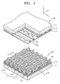
- FIG. 1 illustrates an exploded perspective view of a PDP according to an embodiment of the present invention
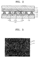
- FIG. 2 illustrates a cross-sectional view along line II-II of the PDP of FIG. 1 ;
- FIG. 3 illustrates a SEM image of a protective layer according to an embodiment of the present invention
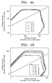
- FIGS. 4A-4B illustrate graphs of wall charge retention capabilities of protective layers of Example 1 and Comparative Example 1, respectively.
- FIG. 5 illustrates a graph of secondary electron emission characteristics of a protective layer of Example 1.
- a protective layer according to an embodiment of the present invention may have a single-layered structure, and may include magnesium oxide (MgO).
- the protective layer may include first magnesium oxide crystals doped with a first impurity and second magnesium oxide crystals doped with a second impurity.
- Magnesium oxide may exhibit excellent plasma resistance and high light transmissivity. Accordingly, when the protective layer of the present invention is used in, e.g., a plasma display panel, transmission of visible light through the protective layer, e.g., light generated by photoluminescent materials to form images on a screen, may be facilitated.
- the first and second magnesium oxide crystals may be at different crystal states, and the first and second impurities may be different from each other.
- the first magnesium oxide crystals with the first impurity and the second magnesium oxide crystals with the second impurity may be present in the single-layered structure of the protective layer simultaneously.
- the protective layer may include a single layer of magnesium oxide having magnesium oxide crystals at different crystal states and with different impurities.
- the first impurity in the first magnesium oxide crystals may be in an amount of about 100 ppm to about 1000 ppm with respect to the first magnesium oxide crystals.
- the first impurity may include a material capable of functioning as an electron trap.
- Examples of the first impurity may include one or more of scandium (Sc), silicon (Si), and/or germanium (Ge). Accordingly, the first magnesium oxide crystals with the first impurity may exhibit excellent secondary electron emission characteristics, i.e., characteristics related to voltage required to initiate discharge and voltage required to sustain discharge.
- the second impurity in the second magnesium oxide crystals may be in an amount of about 100 ppm to about 1000 ppm with respect to the magnesium oxide crystals.
- the second impurity may include a material capable of functioning as a hole trap.
- Examples of the second impurity may include one or more of chromium (Cr), lithium (Li), and/or sodium (Na). Accordingly, the second magnesium oxide crystals with the second impurity may exhibit superior wall charge retention capabilities.
- the first magnesium oxide crystals with the first impurity and the second magnesium oxide crystals with the second impurity may coexist in different crystal states in a single layer. Crystal states of the first and second magnesium oxides may be determined with respect to energy levels of the first and second magnesium oxides, respectively.
- the first magnesium oxide crystals doped with the first impurity may improve secondary electron emission characteristics
- the second magnesium oxide crystals doped with the second impurity may improve wall charge retention capabilities.
- a weight ratio of the first impurity to the second impurity in the protective layer may be in the range of about 1:0.01 to about 1:1.
- the protective layer may include the first impurity to the second impurity in a weight ratio of about 1:0.2.
- An increase in an amount of the first impurity in the protective layer may increase secondary electron emission characteristics therein.
- An increase in an amount of the second impurity in the protective layer may increase wall charge retention capabilities therein, while decreasing secondary electron emission characteristics in the protective layer.
- the weight ratio of the first impurity to the second impurity in the protective layer may be optimized to provide both improved secondary electron emission characteristics and enhanced wall charge retention capabilities. Further, the weight ratio may be adjusted with respect to different magnesium oxide crystals, e.g., crystal states, and/or different impurities.
- the protective layer according to embodiments of the present invention may be advantageous in providing both excellent electron emission characteristics and superior wall charge accumulation capabilities.
- the first and second impurities may not function both as electron traps and hole traps in the single crystal state of the magnesium oxide crystals.
- the protective layer according to embodiments of the present invention may include the first and second impurities in different crystal states of the magnesium oxide crystals.
- a protective layer having a first impurity in first magnesium oxide crystals of one crystal state coexisting with a second impurity in second magnesium oxide crystals of a different crystal state in a single layer may cause the first and second impurities to function as electron traps and hole traps, respectively.
- both electron emission characteristics and wall charge accumulation capabilities of the layer may be substantially improved.
- a method of manufacturing the protective layer may be as follows.
- the first magnesium oxide crystals may be doped with the first impurity to form first pellets.
- the second magnesium oxide crystals may be doped with the second impurity to form second pellets.
- the first and second pellets may be used to form the protective layer.
- high purity magnesium oxide powder may be mixed with another powder including the first impurity, a binder, and an organic solvent to form a first mixture.
- the first impurity is scandium
- scandium salt e.g., scandium oxide (Sc 2 O 3 ) or scandium nitrate (Sc(NO 3 ) 3
- the binder may include, e.g., one or more of polyethylene glycol, polyvinyl butyral, or the like.
- the organic solvent may include, e.g., one or more of ethanol, propanol, or the like.
- the first mixture may be heated at a temperature of about 400 °C to about 500 °C.
- the heated first mixture may be sintered at a temperature of about 1000 °C to about 2000 °C to form the first pellets.
- the method of forming the second pellets may be substantially similar to the method of forming the first pellets, with the exception of using a powder including the second impurity instead of the first impurity.
- the second impurity is chromium, chromium salt, e.g., chromium oxide (Cr 2 O 3 ) or chromium nitrate (Cr(NO 3 ) 3 )
- the first and second pellets may include magnesium oxide crystals at different crystal states.
- the first and second pellets may be deposited simultaneously by a co-deposition method to form a single layer and to selectively grow crystals.
- co-deposition methods may include a co-evaporation method, a co-sputtering method, a co-ion plating method, and so forth.
- a co-pellet including both the first and second magnesium oxide crystals may be deposited, e.g., by evaporation, sputtering, ion plating, and so forth, to grow a single layer including both the first and second magnesium oxide crystals.
- the co-pellet may be formed by preparing first granules with the first impurity and second granules with the second impurity, and by placing the first and second granules in a mold under a predetermined pressure to form the co-pellet.
- FIGS. 1-2 illustrate perspective and cross-sectional views, respectively, of a PDP according to an embodiment of the present invention.
- the PDP includes upper and lower panels 150 and 160 facing one another.
- the upper panel 150 includes a plurality of sustain discharge electrodes 120 along a first direction, e.g., along the x-axis, a first dielectric layer 113, and a protective layer 115 on a first substrate 111.
- the lower panel 160 includes a plurality of address electrodes 173 along a second direction, e.g., along the y-axis, a second dielectric layer 175, and barrier ribs 180 on a second substrate 171.
- the protective layer 115 in the upper panel 150 may be formed according to embodiments of the present invention as described previously, and therefore, its detailed description will not be repeated.
- the protective layer 115 may increase lifetime of the PDP and lower voltage required to initiate discharge with a high secondary electron emission coefficient.
- the first and second substrates 111 and 171 of the PDP face each other, and are formed of any material having excellent light permeability, e.g., a soda lime glass.
- the first and/or second substrates 111 and 171 may be colored in order to reduce reflection of external light, so bright room contrast may be improved.
- the sustain discharge electrodes 120 of the PDP are parallel to each other in this embodiment.
- the sustain discharge electrodes 120 include pairs of X and Y electrodes, e.g., in an alternating pattern.
- Each X and Y electrode includes a transparent electrode 123 and a bus electrode 121.
- the transparent electrodes 123 may be formed of a material having high visible light transmissivity and low electrode resistance, e.g., indium tin oxide.
- the bus electrodes 121 are formed on the transparent electrode to face the second panel 160, and may be formed of, e.g., chromium (Cr), copper (Cu), and aluminum (Al).
- the bus electrodes 121 may compensate for a relatively large resistance of the transparent electrodes 123, so a substantially uniform voltage may be applied to a plurality of discharge cells 190 between the first and second panels 150 and 160. Voltage may be applied to the transparent electrodes 123 to generate and sustain a discharge in the discharge cells 190.
- the first dielectric layer 113 is formed to cover the sustain discharge electrodes 120, so the sustain discharge electrodes 120 is between the first substrate 111 and the first dielectric layer 113.
- discharge current may be restricted in order to sustain glow discharge, and memory function and voltage may be reduced by wall charge accumulation. Withstand voltage and visible light transmissivity may be high in order to increase discharge efficiency.
- the address electrodes 173 of the PDP are parallel to each on the second substrate 171 in this embodiment.
- the address electrode 173 are formed of a conductive material, e.g., Cr, Cu, and/or Al, to provide a substantially uniform voltage to the discharge cells.
- the second dielectric layer 175 of the PDP is formed to cover the address electrodes 173, so the address electrodes 173 are between the second substrate 171 and the second dielectric layer 175. Accordingly, the address electrodes 173 may be shielded from collisions with charged particles. In the second dielectric layer 175, discharge current may be restricted in order to sustain glow discharge, and memory function and voltage may be reduced by wall charge accumulation.
- the barrier ribs 180 of the PDP are formed on the second dielectric layer 175 to partition a discharge space between the first and second substrates 111 and 171 into the discharge cells 190.
- the barrier ribs 180 are arranged in any suitable pattern, so the discharge cells 190 may form, e.g., a matrix.
- the discharge cells 190 may have any suitable cross-section, e.g., a circle, a quadrangle, or any other polygon.
- the discharge cells 190 include photoluminescent layers 177 therein. More specifically, a photoluminescent layer 177, e.g., a fluorescent layer, may be disposed in each of the discharge cells 190.
- red, green, and blue photoluminescent layers 177R, 177G, and 177B may be alternately deposited in the discharge cells 190 to form red, green, and blue discharge cells 190R, 190G, and 190B, respectively.
- a discharge gas e.g., one or more of neon (Ne), xenon (Xe), and/or helium (He), may be injected into the discharge cells 190.
- Example 1 a protective layer according to an embodiment of the present invention was prepared as follows. First, high purity magnesium oxide powder (MgO, 99.995%) was mixed with high purity scandium salt powder (Sc 2 O 3 , 99.999%), polyethylene glycol, and ethanol to form a first mixture. The scandium salt powder was used in an amount of 200 ppm with respect to the magnesium oxide powder. The first mixture was heated at a temperature of 450°C and sintered at a temperature of 1650°C to form first pellets.
- MgO high purity magnesium oxide powder
- Sc 2 O 3 high purity scandium salt powder
- high purity magnesium oxide powder MgO, 99.995%
- high purity chromium salt powder Cr 2 O 3 , 99.999%
- polyethylene glycol polyethylene glycol
- ethanol ethanol
- the chromium salt powder was used in an amount of 100 ppm with respect to the magnesium oxide powder.
- the second mixture was heated to at a temperature of 450°C and sintered at a temperature of 1650°C to form the second pellet. Equal amounts of solvent were used to prepare the first and second pellets.
- the first and second pellets were mixed to form a co-pellet.
- the weight ratio of the scandium salt powder to the chromium salt powder in the co-pellet was 1:0.2.
- the co-pellet was deposited to form a single-layered protective layer.
- the co-pellet was deposited as a single-layered protective layer on a first substrate including a dielectric layer and sustain discharge electrodes.
- a scanning electron microscope (SEM) image of the formed protective layer is illustrated in FIG. 3 .
- the separate first and second magnesium oxide crystals in the formed protective layer are indicated by (A) and (B), respectively, in FIG. 3 .
- References A and B can be discriminated by SIMS (Secondary ion mass spectrometry) in the Figure 3 .
- Comparative Example 1 magnesium oxide powder (MgO, 99.995%) was mixed with silicon powder (Si, 99.999%) to form a third mixture.
- the third mixture was deposited to form a protective layer having a single impurity in magnesium oxide crystals at a single crystal state.
- Example 1 and Comparative Example 1 were compared in terms of wall charge retention capabilities. Results are illustrated in FIGS. 4A-4B . In addition, the protective layer of Example 1 was evaluated in terms of secondary electron emission characteristics. Results are illustrated in FIG. 5 .
- Example 1 and Comparative Example 1 were incorporated into substantially identical PDPs, followed by application of a sustain voltage of 300 V to the X and Y electrodes and measurement of a voltage transfer curve (VTC).
- VTC voltage transfer curve
- voltage potential between address (a) electrodes and respective Y electrodes was measured with respect to voltage potential between respective Y and X electrodes during a period of at least 2000 ⁇ s to determine voltage due to wall charge retention.
- Curves (a)-(d) in FIGS. 4A-4B correspond to scan times of 50 ⁇ s, 500 ⁇ s, 1000 ⁇ s, and 2000 ⁇ s, respectively.
- curve (e) was obtained by floating the address electrodes.
- the VTC of Example 1 As illustrated in the graphs of FIGS. 4A-4B , the VTC of Example 1, as compared to the Comparative Example 1, exhibited an improved wall charge retention capability.
- the voltage potential in Comparative Example 1 between the address and Y electrodes during a period of about 2000 ⁇ s varied to have a value greater than about 80 V, so a loss of wall charges was indicated.
- a voltage potential in Example 1 between the address and Y electrodes during a period of about 2000 ⁇ s was very small, i.e., curves (a)-(d) were substantially close to each other.
- curves (a)-(d) were substantially close to each other.
- the protective layer of Example 1 was evaluated in terms of secondary electron emission characteristics by varying the amount of scandium (Sc) therein, followed by measurement of a secondary electron emission coefficient.
- a weight of Sc was varied from about 30 ppm of Sc in the first magnesium oxide pellet to about 90 ppm of Sc in the first magnesium oxide pellet.
- secondary electron emission coefficient increased according to an increased amount of Sc.
- a protective layer formed according to embodiments of the present invention may have improved secondary electron emission characteristics in addition to enhanced wall charge retention capabilities.
- a protective layer according to embodiments of the present invention may exhibit both superior wall charge retention capabilities and excellent secondary electron emission characteristics. Further, the present invention may provide a method of effectively preparing a single-layered protective layer using a deposition of a co-pellet of different magnesium oxide crystals doped with different impurities or a co-deposition of two pellets of different magnesium oxide crystals doped with different impurities.
- the protective layer according to embodiments of the present invention may be advantageous in providing a substantially minimized waste of power consumption and reduced address discharge time by increasing a secondary electron emission coefficient and improving wall charge retention capabilities. Thus, a PDP having improved reliability and productivity may be produced.
Landscapes
- Engineering & Computer Science (AREA)
- Physics & Mathematics (AREA)
- Plasma & Fusion (AREA)
- Manufacturing & Machinery (AREA)
- Gas-Filled Discharge Tubes (AREA)
Abstract
A protective layer for a plasma display panel (PDP) includes a single layer having a first magnesium oxide crystal doped with a first impurity and a second magnesium oxide crystal doped with a second impurity.
Description
- Embodiments of the present invention relate to a protective layer for a plasma display panel having improved wall charge retention capabilities and enhanced secondary electron emission characteristics.
- Plasma display panels (PDPs) may refer to flat display panels exhibiting improved structure, e.g., large and thin screens, and enhanced display properties, e.g., high brightness, high contrast, wide viewing angle, wide color reproduction range, and so forth. The PDPs may display images via a gas discharge phenomenon. In particular, PDPs may generate vacuum ultraviolet (VUV) light by applying a high-frequency voltage to a discharge gas, so the VUV light may trigger light emission from a photoluminescent material to form an image.
- A conventional PDP may include electrodes and the photoluminescent material between two substrates. The conventional PDP may further include a protective layer between the substrates to shield, e.g., the electrodes. An increase of secondary electron emission characteristics in the conventional protective layer, however, may reduce charge retention capabilities therein, and therefore, may cause malfunction of the PDP.
- Embodiments of the present invention are therefore directed to a protective layer, a method of manufacturing the same, and a PDP including the same, which substantially overcome one or more of the disadvantages and shortcomings of the related art.
- It is therefore a feature of an embodiment of the present invention to provide a protective layer having both excellent secondary electron emission characteristics and superior wall charge retention capabilities.
- It is therefore another feature of an embodiment of the present invention to provide a method of manufacturing a protective layer having both excellent secondary electron emission characteristics and superior wall charge retention capabilities.
- It is yet another feature of an embodiment of the present invention to provide a PDP including a protective layer having both excellent secondary electron emission characteristics and superior wall charge retention capabilities.
- At least one of the above and other features and advantages of the present invention may be realized by providing a protective layer for a PDP, including a single layer having a first magnesium oxide crystal doped with a first impurity and a second magnesium oxide crystal doped with a second impurity. The second magnesium oxide crystal may have a different crystal state than the first magnesium oxide crystal. The first impurity may be different from the second impurity. The first impurity may include a material functioning as an electron trap. The first impurity may include one or more of scandium, silicon, and/or germanium. The second impurity may include a material functioning as a hole trap. The second impurity may include one or more of chromium, lithium, and/or sodium. An amount of the first impurity in the first magnesium oxide crystals may be about 100 ppm to about 1000 ppm. A weight ratio of the first impurity to the second impurity in the protective layer may be about 1:0.01 to about 1:1.
- At least one of the above and other features and advantages of the present invention may be also realized by providing a method of manufacturing a protective layer for a PDP, including doping first magnesium oxide crystals with a first impurity to form first pellets, and doping second magnesium oxide crystals with a second impurity to form second pellets, and depositing the first and second pellets to form a single layer. Depositing the first and second pellets may include simultaneous deposition of the first and second pellets. The method may further include mixing the first and second pellets before depositing the first and second pellets.
- At least one of the above and other features and advantages of the present invention may be further realized by providing a PDP, including a first substrate facing a second substrate, barrier ribs between the first and second substrates, a plurality of electrodes between the first and second substrates, and a protective layer having a single layer structure between the first and second substrates, the protective layer including a first magnesium oxide crystal doped with a first impurity and a second magnesium oxide crystal doped with a second impurity. The first impurity may include a material functioning as an electron trap. The second impurity may include a material functioning as a hole trap. The plurality of electrodes may include pairs of sustain discharge electrodes on the first substrate and address electrodes on the second substrate. The PDP may further include a dielectric layer between the first and second substrates, the protective layer being on the dielectric layer. The dielectric layer may be between the first substrate and the protective layer. The PDP may further include a second dielectric layer on the second substrate.
- According to a first aspect of the invention there is provided a protective layer as set out in Claim 1. Preferred features of this aspect are set out in Claims 2 - 9.
- According to a second aspect of the invention there is provided a method of manufacturing a protective layer as set out in
Claim 10. Preferred features of this aspect are set out in Claims 11 and 12. - According to a third aspect of the invention there is provided a plasma display panel as set out in Claim 13. Preferred features of this aspect are set out in Claims 14 - 17.
- The above and other features and advantages of the present invention will become more apparent to those of ordinary skill in the art by describing in detail exemplary embodiments thereof with reference to the attached drawings, in which:
-
FIG. 1 illustrates an exploded perspective view of a PDP according to an embodiment of the present invention; -
FIG. 2 illustrates a cross-sectional view along line II-II of the PDP ofFIG. 1 ; -
FIG. 3 illustrates a SEM image of a protective layer according to an embodiment of the present invention; -
FIGS. 4A-4B illustrate graphs of wall charge retention capabilities of protective layers of Example 1 and Comparative Example 1, respectively; and -
FIG. 5 illustrates a graph of secondary electron emission characteristics of a protective layer of Example 1. - Embodiments of the present invention will now be described more fully hereinafter with reference to the accompanying drawings, in which exemplary embodiments of the invention are illustrated. Aspects of the invention may, however, be embodied in different forms and should not be construed as limited to the embodiments set forth herein. Rather, these embodiments are provided so that this disclosure will be thorough and complete, and will fully convey the scope of the invention to those skilled in the art.
- In the figures, the dimensions of layers, elements, and regions may be exaggerated for clarity of illustration. It will also be understood that when a layer or element is referred to as being "on" another layer, element, or substrate, it can be directly on the other layer, element, or substrate, or intervening layers and/or elements may also be present. Further, it will be understood that when a layer or element is referred to as being "under" another layer or element, it can be directly under, or one or more intervening layers and/or elements may also be present. In addition, it will also be understood that when a layer or element is referred to as being "between" two layers or elements, it can be the only layer or element between the two layers or elements, or one or more intervening layers and/or elements may also be present. Like reference numerals refer to like elements throughout.
- A protective layer according to an embodiment of the present invention may have a single-layered structure, and may include magnesium oxide (MgO). In particular, the protective layer may include first magnesium oxide crystals doped with a first impurity and second magnesium oxide crystals doped with a second impurity. Magnesium oxide may exhibit excellent plasma resistance and high light transmissivity. Accordingly, when the protective layer of the present invention is used in, e.g., a plasma display panel, transmission of visible light through the protective layer, e.g., light generated by photoluminescent materials to form images on a screen, may be facilitated.
- The first and second magnesium oxide crystals may be at different crystal states, and the first and second impurities may be different from each other. The first magnesium oxide crystals with the first impurity and the second magnesium oxide crystals with the second impurity may be present in the single-layered structure of the protective layer simultaneously. Accordingly, the protective layer may include a single layer of magnesium oxide having magnesium oxide crystals at different crystal states and with different impurities.
- The first impurity in the first magnesium oxide crystals may be in an amount of about 100 ppm to about 1000 ppm with respect to the first magnesium oxide crystals. The first impurity may include a material capable of functioning as an electron trap. Examples of the first impurity may include one or more of scandium (Sc), silicon (Si), and/or germanium (Ge). Accordingly, the first magnesium oxide crystals with the first impurity may exhibit excellent secondary electron emission characteristics, i.e., characteristics related to voltage required to initiate discharge and voltage required to sustain discharge.
- The second impurity in the second magnesium oxide crystals may be in an amount of about 100 ppm to about 1000 ppm with respect to the magnesium oxide crystals. The second impurity may include a material capable of functioning as a hole trap. Examples of the second impurity may include one or more of chromium (Cr), lithium (Li), and/or sodium (Na). Accordingly, the second magnesium oxide crystals with the second impurity may exhibit superior wall charge retention capabilities.
- The first magnesium oxide crystals with the first impurity and the second magnesium oxide crystals with the second impurity may coexist in different crystal states in a single layer. Crystal states of the first and second magnesium oxides may be determined with respect to energy levels of the first and second magnesium oxides, respectively. Thus, the first magnesium oxide crystals doped with the first impurity may improve secondary electron emission characteristics, and the second magnesium oxide crystals doped with the second impurity may improve wall charge retention capabilities.
- A weight ratio of the first impurity to the second impurity in the protective layer may be in the range of about 1:0.01 to about 1:1. For example, the protective layer may include the first impurity to the second impurity in a weight ratio of about 1:0.2. An increase in an amount of the first impurity in the protective layer may increase secondary electron emission characteristics therein. An increase in an amount of the second impurity in the protective layer may increase wall charge retention capabilities therein, while decreasing secondary electron emission characteristics in the protective layer. Thus, the weight ratio of the first impurity to the second impurity in the protective layer may be optimized to provide both improved secondary electron emission characteristics and enhanced wall charge retention capabilities. Further, the weight ratio may be adjusted with respect to different magnesium oxide crystals, e.g., crystal states, and/or different impurities.
- The protective layer according to embodiments of the present invention may be advantageous in providing both excellent electron emission characteristics and superior wall charge accumulation capabilities. In particular, when magnesium oxide crystals of a single crystal state are doped with both the first and second impurities, the first and second impurities may not function both as electron traps and hole traps in the single crystal state of the magnesium oxide crystals. The protective layer according to embodiments of the present invention, however, may include the first and second impurities in different crystal states of the magnesium oxide crystals. A protective layer having a first impurity in first magnesium oxide crystals of one crystal state coexisting with a second impurity in second magnesium oxide crystals of a different crystal state in a single layer may cause the first and second impurities to function as electron traps and hole traps, respectively. When the first and second impurities function both as electron traps and hole traps, respectively, in a single layer, both electron emission characteristics and wall charge accumulation capabilities of the layer may be substantially improved.
- A method of manufacturing the protective layer may be as follows. The first magnesium oxide crystals may be doped with the first impurity to form first pellets. The second magnesium oxide crystals may be doped with the second impurity to form second pellets. The first and second pellets may be used to form the protective layer.
- More specifically, high purity magnesium oxide powder may be mixed with another powder including the first impurity, a binder, and an organic solvent to form a first mixture. For example, if the first impurity is scandium, scandium salt, e.g., scandium oxide (Sc2O3) or scandium nitrate (Sc(NO3)3), may be used. The binder may include, e.g., one or more of polyethylene glycol, polyvinyl butyral, or the like. The organic solvent may include, e.g., one or more of ethanol, propanol, or the like. The first mixture may be heated at a temperature of about 400 °C to about 500 °C. Then, the heated first mixture may be sintered at a temperature of about 1000 °C to about 2000 °C to form the first pellets. The method of forming the second pellets may be substantially similar to the method of forming the first pellets, with the exception of using a powder including the second impurity instead of the first impurity. For example, if the second impurity is chromium, chromium salt, e.g., chromium oxide (Cr2O3) or chromium nitrate (Cr(NO3)3), may be mixed with the high purity magnesium oxide powder, binder, and organic solvent to form a second mixture for the second pellets. The first and second pellets may include magnesium oxide crystals at different crystal states.
- The first and second pellets may be deposited simultaneously by a co-deposition method to form a single layer and to selectively grow crystals. Examples of co-deposition methods may include a co-evaporation method, a co-sputtering method, a co-ion plating method, and so forth.
- Alternatively, a co-pellet including both the first and second magnesium oxide crystals may be deposited, e.g., by evaporation, sputtering, ion plating, and so forth, to grow a single layer including both the first and second magnesium oxide crystals. The co-pellet may be formed by preparing first granules with the first impurity and second granules with the second impurity, and by placing the first and second granules in a mold under a predetermined pressure to form the co-pellet.
-
FIGS. 1-2 illustrate perspective and cross-sectional views, respectively, of a PDP according to an embodiment of the present invention. Referring toFIGS. 1-2 , the PDP includes upper andlower panels upper panel 150 includes a plurality of sustaindischarge electrodes 120 along a first direction, e.g., along the x-axis, a firstdielectric layer 113, and aprotective layer 115 on afirst substrate 111. Thelower panel 160 includes a plurality ofaddress electrodes 173 along a second direction, e.g., along the y-axis, asecond dielectric layer 175, andbarrier ribs 180 on asecond substrate 171. Theprotective layer 115 in theupper panel 150 may be formed according to embodiments of the present invention as described previously, and therefore, its detailed description will not be repeated. Theprotective layer 115 may increase lifetime of the PDP and lower voltage required to initiate discharge with a high secondary electron emission coefficient. - The first and
second substrates second substrates - The sustain
discharge electrodes 120 of the PDP are parallel to each other in this embodiment. The sustaindischarge electrodes 120 include pairs of X and Y electrodes, e.g., in an alternating pattern. Each X and Y electrode includes atransparent electrode 123 and abus electrode 121. Thetransparent electrodes 123 may be formed of a material having high visible light transmissivity and low electrode resistance, e.g., indium tin oxide. Thebus electrodes 121 are formed on the transparent electrode to face thesecond panel 160, and may be formed of, e.g., chromium (Cr), copper (Cu), and aluminum (Al). Thebus electrodes 121 may compensate for a relatively large resistance of thetransparent electrodes 123, so a substantially uniform voltage may be applied to a plurality ofdischarge cells 190 between the first andsecond panels transparent electrodes 123 to generate and sustain a discharge in thedischarge cells 190. - The
first dielectric layer 113 is formed to cover the sustaindischarge electrodes 120, so the sustaindischarge electrodes 120 is between thefirst substrate 111 and thefirst dielectric layer 113. In thefirst dielectric layer 113, discharge current may be restricted in order to sustain glow discharge, and memory function and voltage may be reduced by wall charge accumulation. Withstand voltage and visible light transmissivity may be high in order to increase discharge efficiency. - The
address electrodes 173 of the PDP are parallel to each on thesecond substrate 171 in this embodiment. Theaddress electrode 173 are formed of a conductive material, e.g., Cr, Cu, and/or Al, to provide a substantially uniform voltage to the discharge cells. - The
second dielectric layer 175 of the PDP is formed to cover theaddress electrodes 173, so theaddress electrodes 173 are between thesecond substrate 171 and thesecond dielectric layer 175. Accordingly, theaddress electrodes 173 may be shielded from collisions with charged particles. In thesecond dielectric layer 175, discharge current may be restricted in order to sustain glow discharge, and memory function and voltage may be reduced by wall charge accumulation. - The
barrier ribs 180 of the PDP are formed on thesecond dielectric layer 175 to partition a discharge space between the first andsecond substrates discharge cells 190. Thebarrier ribs 180 are arranged in any suitable pattern, so thedischarge cells 190 may form, e.g., a matrix. Thedischarge cells 190 may have any suitable cross-section, e.g., a circle, a quadrangle, or any other polygon. Thedischarge cells 190 includephotoluminescent layers 177 therein. More specifically, aphotoluminescent layer 177, e.g., a fluorescent layer, may be disposed in each of thedischarge cells 190. For example, red, green, and blue photoluminescent layers 177R, 177G, and 177B may be alternately deposited in thedischarge cells 190 to form red, green, andblue discharge cells discharge cells 190. - Example 1: a protective layer according to an embodiment of the present invention was prepared as follows. First, high purity magnesium oxide powder (MgO, 99.995%) was mixed with high purity scandium salt powder (Sc2O3, 99.999%), polyethylene glycol, and ethanol to form a first mixture. The scandium salt powder was used in an amount of 200 ppm with respect to the magnesium oxide powder. The first mixture was heated at a temperature of 450°C and sintered at a temperature of 1650°C to form first pellets.
- Next, high purity magnesium oxide powder (MgO, 99.995%) was mixed with high purity chromium salt powder (Cr2O3, 99.999%), polyethylene glycol, and ethanol to form a second mixture. The chromium salt powder was used in an amount of 100 ppm with respect to the magnesium oxide powder. The second mixture was heated to at a temperature of 450°C and sintered at a temperature of 1650°C to form the second pellet. Equal amounts of solvent were used to prepare the first and second pellets.
- Next, the first and second pellets were mixed to form a co-pellet. The weight ratio of the scandium salt powder to the chromium salt powder in the co-pellet was 1:0.2. The co-pellet was deposited to form a single-layered protective layer. The co-pellet was deposited as a single-layered protective layer on a first substrate including a dielectric layer and sustain discharge electrodes. A scanning electron microscope (SEM) image of the formed protective layer is illustrated in
FIG. 3 . The separate first and second magnesium oxide crystals in the formed protective layer are indicated by (A) and (B), respectively, inFIG. 3 . References A and B can be discriminated by SIMS (Secondary ion mass spectrometry) in theFigure 3 . - Comparative Example 1: magnesium oxide powder (MgO, 99.995%) was mixed with silicon powder (Si, 99.999%) to form a third mixture. The third mixture was deposited to form a protective layer having a single impurity in magnesium oxide crystals at a single crystal state.
- The protective layers of Example 1 and Comparative Example 1 were compared in terms of wall charge retention capabilities. Results are illustrated in
FIGS. 4A-4B . In addition, the protective layer of Example 1 was evaluated in terms of secondary electron emission characteristics. Results are illustrated inFIG. 5 . - More specifically, the protective layers of Example 1 and Comparative Example 1 were incorporated into substantially identical PDPs, followed by application of a sustain voltage of 300 V to the X and Y electrodes and measurement of a voltage transfer curve (VTC). During application of the sustain voltage of 300 V, voltage potential between address (a) electrodes and respective Y electrodes was measured with respect to voltage potential between respective Y and X electrodes during a period of at least 2000 µs to determine voltage due to wall charge retention. Curves (a)-(d) in
FIGS. 4A-4B correspond to scan times of 50 µs, 500 µs, 1000 µs, and 2000 µs, respectively. As a control group, curve (e) was obtained by floating the address electrodes. - As illustrated in the graphs of
FIGS. 4A-4B , the VTC of Example 1, as compared to the Comparative Example 1, exhibited an improved wall charge retention capability. In particular, as illustrated inFIG. 4B , the voltage potential in Comparative Example 1 between the address and Y electrodes during a period of about 2000 µs varied to have a value greater than about 80 V, so a loss of wall charges was indicated. In contrast, as illustrated inFIG. 4A , a voltage potential in Example 1 between the address and Y electrodes during a period of about 2000 µs was very small, i.e., curves (a)-(d) were substantially close to each other. Thus, it can be seen that wall charge retention capabilities were increased in Example 1, as compared to Comparative Example 1. - The protective layer of Example 1 was evaluated in terms of secondary electron emission characteristics by varying the amount of scandium (Sc) therein, followed by measurement of a secondary electron emission coefficient. A weight of Sc was varied from about 30 ppm of Sc in the first magnesium oxide pellet to about 90 ppm of Sc in the first magnesium oxide pellet. As illustrated in
FIG. 5 , secondary electron emission coefficient increased according to an increased amount of Sc. Thus, it can be seen that a protective layer formed according to embodiments of the present invention may have improved secondary electron emission characteristics in addition to enhanced wall charge retention capabilities. - As described above, a protective layer according to embodiments of the present invention may exhibit both superior wall charge retention capabilities and excellent secondary electron emission characteristics. Further, the present invention may provide a method of effectively preparing a single-layered protective layer using a deposition of a co-pellet of different magnesium oxide crystals doped with different impurities or a co-deposition of two pellets of different magnesium oxide crystals doped with different impurities. The protective layer according to embodiments of the present invention may be advantageous in providing a substantially minimized waste of power consumption and reduced address discharge time by increasing a secondary electron emission coefficient and improving wall charge retention capabilities. Thus, a PDP having improved reliability and productivity may be produced.
- Exemplary embodiments of the present invention have been disclosed herein, and although specific terms are employed, they are used and are to be interpreted in a generic and descriptive sense only and not for purpose of limitation. Accordingly, it will be understood by those of ordinary skill in the art that various changes in form and details may be made without departing from the scope of the present invention as set forth in the following claims.
Claims (15)
- A protective layer for a plasma display panel (PDP), comprising a single layer having a first magnesium oxide crystal doped with a first impurity and a second magnesium oxide crystal doped with a second impurity.
- A protective layer according to claim 1, wherein the second magnesium oxide crystal has a different crystal state than the first magnesium oxide crystal.
- A protective layer according to claim 1 or 2, wherein the first impurity is different from the second impurity.
- A protective layer according to claim 3, wherein the first impurity includes a material functioning as an electron trap.
- A protective layer according to claim 4, wherein the first impurity includes one or more of scandium, silicon, and/or germanium.
- A protective layer according to any one of claims 3 to 5, wherein the second impurity includes a material functioning as a hole trap.
- A protective layer according to claim 6, wherein the second impurity includes one or more of chromium, lithium, and/or sodium.
- A protective layer according to any one of claims 1 to 7, wherein an amount of the first impurity in the first magnesium oxide crystal is from about 100 ppm to about 1000 ppm.
- A protective layer according to any one of claims 1 to 8, wherein a weight ratio of the first impurity to the second impurity in the protective layer is from about 1:0.01 to about 1:1.
- A method of manufacturing a protective layer for a plasma display panel (PDP), comprising:doping first magnesium oxide crystals with a first impurity to form first pellets;doping second magnesium oxide crystals with a second impurity to form second pellets; anddepositing the first and second pellets to form a single layer.
- A method according to claim 10, wherein depositing the first and second pellets includes simultaneous deposition of the first and second pellets.
- A method according to claim 10 or 11, further comprising mixing the first and second pellets before depositing the first and second pellets.
- A plasma display panel (PDP), comprising:a first substrate facing a second substrate;barrier ribs between the first and second substrates;a plurality of electrodes between the first and second substrates; anda protective layer between the first and second substrates, the protective layer being according to any one of Claims 1 to 9.
- A PDP according to claim 13, wherein the plurality of electrodes includes pairs of sustain discharge electrodes on the first substrate and address electrodes on the second substrate.
- A PDP according to claim 14, further comprising a dielectric layer between the first and second substrates, the protective layer being located on the dielectric layer.
Applications Claiming Priority (1)
| Application Number | Priority Date | Filing Date | Title |
|---|---|---|---|
| KR1020070100866A KR20090035854A (en) | 2007-10-08 | 2007-10-08 | Protective film, manufacturing method thereof and plasma display panel comprising the protective film |
Publications (1)
| Publication Number | Publication Date |
|---|---|
| EP2048687A2 true EP2048687A2 (en) | 2009-04-15 |
Family
ID=40379797
Family Applications (1)
| Application Number | Title | Priority Date | Filing Date |
|---|---|---|---|
| EP08253276A Withdrawn EP2048687A2 (en) | 2007-10-08 | 2008-10-08 | Protective layer, method of manufacturing the same, and plasma display panel including the same |
Country Status (5)
| Country | Link |
|---|---|
| US (1) | US20090091260A1 (en) |
| EP (1) | EP2048687A2 (en) |
| JP (1) | JP2009094073A (en) |
| KR (1) | KR20090035854A (en) |
| CN (1) | CN101409192A (en) |
Family Cites Families (2)
| Publication number | Priority date | Publication date | Assignee | Title |
|---|---|---|---|---|
| WO2005029530A1 (en) * | 2003-09-24 | 2005-03-31 | Matsushita Electric Industrial Co., Ltd. | Plasma display panel |
| KR100603354B1 (en) * | 2004-06-26 | 2006-07-20 | 삼성에스디아이 주식회사 | A composition for forming a PDP protective film, a PDP protective film prepared using the same, a method for preparing a protective film, and a PDP employing the same |
-
2007
- 2007-10-08 KR KR1020070100866A patent/KR20090035854A/en not_active Ceased
-
2008
- 2008-09-22 US US12/232,656 patent/US20090091260A1/en not_active Abandoned
- 2008-10-08 JP JP2008261594A patent/JP2009094073A/en not_active Withdrawn
- 2008-10-08 EP EP08253276A patent/EP2048687A2/en not_active Withdrawn
- 2008-10-08 CN CNA2008101661260A patent/CN101409192A/en active Pending
Also Published As
| Publication number | Publication date |
|---|---|
| KR20090035854A (en) | 2009-04-13 |
| CN101409192A (en) | 2009-04-15 |
| JP2009094073A (en) | 2009-04-30 |
| US20090091260A1 (en) | 2009-04-09 |
Similar Documents
| Publication | Publication Date | Title |
|---|---|---|
| EP2214193B1 (en) | Plasma display panel | |
| US7868550B2 (en) | Protective layer material for PDP and method of manufacturing the same | |
| KR100875114B1 (en) | Materials of protective layer, method of preparing the same, protective layers made from the same and plasma display panel comprising the protective layer | |
| EP2099052B1 (en) | Plasma display panel | |
| KR100603354B1 (en) | A composition for forming a PDP protective film, a PDP protective film prepared using the same, a method for preparing a protective film, and a PDP employing the same | |
| EP2101342A1 (en) | Plasma display panel | |
| US20080088532A1 (en) | Plasma display panel | |
| US20090091260A1 (en) | Protective layer, method of manufacturing the same, and plasma display panel including the same | |
| EP2099051A1 (en) | Plasma display panel | |
| US20090021169A1 (en) | Barrier ribs to reduce reflection of external light and plasma display panel (PDP) including such barrier ribs | |
| EP2120253A1 (en) | Plasma display panel | |
| KR20130052543A (en) | Manufacturing method for plasma display panel | |
| EP2124241B1 (en) | Plasma display panel | |
| KR20070047075A (en) | Protective film of plasma display panel | |
| EP2099049A1 (en) | Method for manufacturing plasma display panel | |
| US20050017640A1 (en) | Plasma display panel and fabrication method thereof | |
| CN103236387A (en) | Gas discharge compound dielectric protective layer and plasma display panel comprising same | |
| US8058805B2 (en) | Plasma display panel | |
| US20100164361A1 (en) | Plasma display panel protective layer | |
| KR100814855B1 (en) | Magnesium oxide sintered body, and plasma display panel manufactured using the same | |
| US7649315B2 (en) | Plasma display panel | |
| KR100649522B1 (en) | Plasma display panel | |
| US20080143257A1 (en) | Plasma display panel | |
| EP2081210B1 (en) | Plasma display panel | |
| KR100709210B1 (en) | Plasma display panel |
Legal Events
| Date | Code | Title | Description |
|---|---|---|---|
| PUAI | Public reference made under article 153(3) epc to a published international application that has entered the european phase |
Free format text: ORIGINAL CODE: 0009012 |
|
| 17P | Request for examination filed |
Effective date: 20081014 |
|
| AK | Designated contracting states |
Kind code of ref document: A2 Designated state(s): AT BE BG CH CY CZ DE DK EE ES FI FR GB GR HR HU IE IS IT LI LT LU LV MC MT NL NO PL PT RO SE SI SK TR |
|
| AX | Request for extension of the european patent |
Extension state: AL BA MK RS |
|
| STAA | Information on the status of an ep patent application or granted ep patent |
Free format text: STATUS: THE APPLICATION HAS BEEN WITHDRAWN |
|
| 18W | Application withdrawn |
Effective date: 20091218 |