EP2046101A1 - A surface dielectric barrier discharge plasma unit and a method of generating a surface plasma - Google Patents
A surface dielectric barrier discharge plasma unit and a method of generating a surface plasma Download PDFInfo
- Publication number
- EP2046101A1 EP2046101A1 EP07112805A EP07112805A EP2046101A1 EP 2046101 A1 EP2046101 A1 EP 2046101A1 EP 07112805 A EP07112805 A EP 07112805A EP 07112805 A EP07112805 A EP 07112805A EP 2046101 A1 EP2046101 A1 EP 2046101A1
- Authority
- EP
- European Patent Office
- Prior art keywords
- solid dielectric
- plasma
- exterior
- plasma unit
- unit according
- Prior art date
- Legal status (The legal status is an assumption and is not a legal conclusion. Google has not performed a legal analysis and makes no representation as to the accuracy of the status listed.)
- Withdrawn
Links
- 230000004888 barrier function Effects 0.000 title claims abstract description 55
- 238000000034 method Methods 0.000 title claims description 29
- 239000007787 solid Substances 0.000 claims abstract description 130
- 230000008569 process Effects 0.000 claims description 26
- 230000003750 conditioning effect Effects 0.000 claims description 17
- 239000012530 fluid Substances 0.000 claims description 14
- 239000003792 electrolyte Substances 0.000 claims description 12
- 239000004020 conductor Substances 0.000 claims description 2
- 230000001939 inductive effect Effects 0.000 claims 1
- 210000002381 plasma Anatomy 0.000 description 147
- 239000007789 gas Substances 0.000 description 106
- 239000002245 particle Substances 0.000 description 15
- 239000000463 material Substances 0.000 description 13
- 238000011282 treatment Methods 0.000 description 13
- 229910052751 metal Inorganic materials 0.000 description 11
- 239000002184 metal Substances 0.000 description 11
- 238000000151 deposition Methods 0.000 description 9
- 230000008021 deposition Effects 0.000 description 9
- 238000009832 plasma treatment Methods 0.000 description 9
- 239000002243 precursor Substances 0.000 description 8
- 238000004519 manufacturing process Methods 0.000 description 7
- 238000001816 cooling Methods 0.000 description 6
- 230000005684 electric field Effects 0.000 description 5
- 239000000203 mixture Substances 0.000 description 5
- 239000000919 ceramic Substances 0.000 description 4
- 238000000576 coating method Methods 0.000 description 4
- 239000003989 dielectric material Substances 0.000 description 4
- 238000002347 injection Methods 0.000 description 4
- 239000007924 injection Substances 0.000 description 4
- 239000007788 liquid Substances 0.000 description 4
- 238000006116 polymerization reaction Methods 0.000 description 4
- 238000004659 sterilization and disinfection Methods 0.000 description 4
- 230000003197 catalytic effect Effects 0.000 description 3
- 239000003344 environmental pollutant Substances 0.000 description 3
- 238000001125 extrusion Methods 0.000 description 3
- 231100000719 pollutant Toxicity 0.000 description 3
- 239000000126 substance Substances 0.000 description 3
- 239000004593 Epoxy Substances 0.000 description 2
- VYPSYNLAJGMNEJ-UHFFFAOYSA-N Silicium dioxide Chemical compound O=[Si]=O VYPSYNLAJGMNEJ-UHFFFAOYSA-N 0.000 description 2
- PPBRXRYQALVLMV-UHFFFAOYSA-N Styrene Chemical compound C=CC1=CC=CC=C1 PPBRXRYQALVLMV-UHFFFAOYSA-N 0.000 description 2
- 230000004913 activation Effects 0.000 description 2
- 238000004026 adhesive bonding Methods 0.000 description 2
- PNEYBMLMFCGWSK-UHFFFAOYSA-N aluminium oxide Inorganic materials [O-2].[O-2].[O-2].[Al+3].[Al+3] PNEYBMLMFCGWSK-UHFFFAOYSA-N 0.000 description 2
- 230000009286 beneficial effect Effects 0.000 description 2
- 230000015572 biosynthetic process Effects 0.000 description 2
- 238000006243 chemical reaction Methods 0.000 description 2
- 239000011248 coating agent Substances 0.000 description 2
- 150000001875 compounds Chemical class 0.000 description 2
- 238000000354 decomposition reaction Methods 0.000 description 2
- 230000001419 dependent effect Effects 0.000 description 2
- 239000000428 dust Substances 0.000 description 2
- 230000003628 erosive effect Effects 0.000 description 2
- 239000000835 fiber Substances 0.000 description 2
- 239000011888 foil Substances 0.000 description 2
- 239000000446 fuel Substances 0.000 description 2
- 238000010438 heat treatment Methods 0.000 description 2
- 230000006872 improvement Effects 0.000 description 2
- 239000008263 liquid aerosol Substances 0.000 description 2
- 238000003801 milling Methods 0.000 description 2
- BASFCYQUMIYNBI-UHFFFAOYSA-N platinum Chemical compound [Pt] BASFCYQUMIYNBI-UHFFFAOYSA-N 0.000 description 2
- 238000009877 rendering Methods 0.000 description 2
- 230000001954 sterilising effect Effects 0.000 description 2
- 238000004347 surface barrier Methods 0.000 description 2
- 238000011144 upstream manufacturing Methods 0.000 description 2
- 239000002028 Biomass Substances 0.000 description 1
- QDCUCTAMIYGWQS-UHFFFAOYSA-N C=CC=C.[N] Chemical compound C=CC=C.[N] QDCUCTAMIYGWQS-UHFFFAOYSA-N 0.000 description 1
- RYGMFSIKBFXOCR-UHFFFAOYSA-N Copper Chemical compound [Cu] RYGMFSIKBFXOCR-UHFFFAOYSA-N 0.000 description 1
- 229910000677 High-carbon steel Inorganic materials 0.000 description 1
- UFHFLCQGNIYNRP-UHFFFAOYSA-N Hydrogen Chemical compound [H][H] UFHFLCQGNIYNRP-UHFFFAOYSA-N 0.000 description 1
- 229910016978 MnOx Inorganic materials 0.000 description 1
- 239000003463 adsorbent Substances 0.000 description 1
- 239000000443 aerosol Substances 0.000 description 1
- 238000004378 air conditioning Methods 0.000 description 1
- 229910045601 alloy Inorganic materials 0.000 description 1
- 239000000956 alloy Substances 0.000 description 1
- 239000007864 aqueous solution Substances 0.000 description 1
- 238000010923 batch production Methods 0.000 description 1
- 230000008901 benefit Effects 0.000 description 1
- 239000012159 carrier gas Substances 0.000 description 1
- 230000015556 catabolic process Effects 0.000 description 1
- 230000008859 change Effects 0.000 description 1
- 238000002144 chemical decomposition reaction Methods 0.000 description 1
- 239000012707 chemical precursor Substances 0.000 description 1
- 239000013626 chemical specie Substances 0.000 description 1
- 238000004140 cleaning Methods 0.000 description 1
- 229910052681 coesite Inorganic materials 0.000 description 1
- 239000000567 combustion gas Substances 0.000 description 1
- 230000001143 conditioned effect Effects 0.000 description 1
- 229910052802 copper Inorganic materials 0.000 description 1
- 239000010949 copper Substances 0.000 description 1
- ARUVKPQLZAKDPS-UHFFFAOYSA-L copper(II) sulfate Chemical compound [Cu+2].[O-][S+2]([O-])([O-])[O-] ARUVKPQLZAKDPS-UHFFFAOYSA-L 0.000 description 1
- 230000007797 corrosion Effects 0.000 description 1
- 238000005260 corrosion Methods 0.000 description 1
- 230000008878 coupling Effects 0.000 description 1
- 238000010168 coupling process Methods 0.000 description 1
- 238000005859 coupling reaction Methods 0.000 description 1
- 229910052906 cristobalite Inorganic materials 0.000 description 1
- 238000004132 cross linking Methods 0.000 description 1
- 230000003247 decreasing effect Effects 0.000 description 1
- 230000007547 defect Effects 0.000 description 1
- 238000005137 deposition process Methods 0.000 description 1
- 238000009826 distribution Methods 0.000 description 1
- 230000005672 electromagnetic field Effects 0.000 description 1
- 239000003822 epoxy resin Substances 0.000 description 1
- 238000011049 filling Methods 0.000 description 1
- 238000001914 filtration Methods 0.000 description 1
- 239000012634 fragment Substances 0.000 description 1
- 238000012685 gas phase polymerization Methods 0.000 description 1
- 239000011521 glass Substances 0.000 description 1
- 239000006112 glass ceramic composition Substances 0.000 description 1
- 239000000156 glass melt Substances 0.000 description 1
- 239000003292 glue Substances 0.000 description 1
- 229930195733 hydrocarbon Natural products 0.000 description 1
- 150000002430 hydrocarbons Chemical class 0.000 description 1
- 229910052739 hydrogen Inorganic materials 0.000 description 1
- 239000001257 hydrogen Substances 0.000 description 1
- 239000004434 industrial solvent Substances 0.000 description 1
- 238000002955 isolation Methods 0.000 description 1
- 238000005304 joining Methods 0.000 description 1
- 239000011244 liquid electrolyte Substances 0.000 description 1
- 150000002739 metals Chemical class 0.000 description 1
- 244000005700 microbiome Species 0.000 description 1
- 230000001590 oxidative effect Effects 0.000 description 1
- 230000035515 penetration Effects 0.000 description 1
- 230000010363 phase shift Effects 0.000 description 1
- 229910052697 platinum Inorganic materials 0.000 description 1
- 229920000647 polyepoxide Polymers 0.000 description 1
- 229920000642 polymer Polymers 0.000 description 1
- 239000011148 porous material Substances 0.000 description 1
- 238000002203 pretreatment Methods 0.000 description 1
- 238000004886 process control Methods 0.000 description 1
- 230000036632 reaction speed Effects 0.000 description 1
- 230000009257 reactivity Effects 0.000 description 1
- 230000003134 recirculating effect Effects 0.000 description 1
- 230000009467 reduction Effects 0.000 description 1
- 230000003252 repetitive effect Effects 0.000 description 1
- 230000000630 rising effect Effects 0.000 description 1
- 239000000377 silicon dioxide Substances 0.000 description 1
- 235000012239 silicon dioxide Nutrition 0.000 description 1
- 239000004071 soot Substances 0.000 description 1
- 241000894007 species Species 0.000 description 1
- -1 stainless steel Chemical class 0.000 description 1
- 239000010935 stainless steel Substances 0.000 description 1
- 229910001220 stainless steel Inorganic materials 0.000 description 1
- 229910052682 stishovite Inorganic materials 0.000 description 1
- 239000000725 suspension Substances 0.000 description 1
- 239000004753 textile Substances 0.000 description 1
- 230000003685 thermal hair damage Effects 0.000 description 1
- 229910052905 tridymite Inorganic materials 0.000 description 1
- WFKWXMTUELFFGS-UHFFFAOYSA-N tungsten Chemical compound [W] WFKWXMTUELFFGS-UHFFFAOYSA-N 0.000 description 1
- 229910052721 tungsten Inorganic materials 0.000 description 1
- 239000010937 tungsten Substances 0.000 description 1
- 238000009827 uniform distribution Methods 0.000 description 1
- 239000012855 volatile organic compound Substances 0.000 description 1
- 239000010457 zeolite Substances 0.000 description 1
Images




Classifications
-
- H—ELECTRICITY
- H05—ELECTRIC TECHNIQUES NOT OTHERWISE PROVIDED FOR
- H05H—PLASMA TECHNIQUE; PRODUCTION OF ACCELERATED ELECTRICALLY-CHARGED PARTICLES OR OF NEUTRONS; PRODUCTION OR ACCELERATION OF NEUTRAL MOLECULAR OR ATOMIC BEAMS
- H05H1/00—Generating plasma; Handling plasma
- H05H1/24—Generating plasma
- H05H1/2406—Generating plasma using dielectric barrier discharges, i.e. with a dielectric interposed between the electrodes
- H05H1/2437—Multilayer systems
-
- H—ELECTRICITY
- H05—ELECTRIC TECHNIQUES NOT OTHERWISE PROVIDED FOR
- H05H—PLASMA TECHNIQUE; PRODUCTION OF ACCELERATED ELECTRICALLY-CHARGED PARTICLES OR OF NEUTRONS; PRODUCTION OR ACCELERATION OF NEUTRAL MOLECULAR OR ATOMIC BEAMS
- H05H1/00—Generating plasma; Handling plasma
- H05H1/24—Generating plasma
- H05H1/2406—Generating plasma using dielectric barrier discharges, i.e. with a dielectric interposed between the electrodes
- H05H1/2439—Surface discharges, e.g. air flow control
-
- H—ELECTRICITY
- H05—ELECTRIC TECHNIQUES NOT OTHERWISE PROVIDED FOR
- H05H—PLASMA TECHNIQUE; PRODUCTION OF ACCELERATED ELECTRICALLY-CHARGED PARTICLES OR OF NEUTRONS; PRODUCTION OR ACCELERATION OF NEUTRAL MOLECULAR OR ATOMIC BEAMS
- H05H1/00—Generating plasma; Handling plasma
- H05H1/24—Generating plasma
- H05H1/2406—Generating plasma using dielectric barrier discharges, i.e. with a dielectric interposed between the electrodes
- H05H1/2418—Generating plasma using dielectric barrier discharges, i.e. with a dielectric interposed between the electrodes the electrodes being embedded in the dielectric
Definitions
- the invention relates to a surface dielectric barrier discharge plasma unit comprising a solid dielectric structure provided with an interior space wherein an interior electrode is arranged, further comprising a further electrode for generating in concert with the interior electrode a surface dielectric barrier discharge plasma, wherein the plasma unit is further provided with a gas flow path along a surface of the structure.
- Solid dielectric structures having electrode structures arranged on or embedded in the dielectric structures are known for performing plasma processes.
- a first electrode is positioned on a treating surface of the structure, while a second electrode is placed on the opposite side of the dielectric structure.
- gas flows needed for the plasma process can be induced along a treating surface of the structure.
- Dedicated plasma units having an interior electrode are also known.
- the interior electrode is obtained via a process wherein dielectric material is partially removed for forming a groove in a surface of the dielectric structure, an electrode deposition process and a process wherein the interior electrode is covered with dielectric material to obtain a flat dielectric surface.
- a second electrode is placed on the opposite side of the dielectric structure.
- Dedicated plasma units having only interior electrodes are also known. By creating an electric field between pairs of interior electrodes a plasma process can be induced along a treating surface of the structure.
- plasma treatments appear to be non-uniform, especially when treating structures having low or non-gas permeable materials.
- the gas flow is flown in a plasma zone between the structure to be treated and a treating surface of the solid dielectric structure and reacts chemically and/or physically with the structure to be treated.
- less reactive gas particles are available in a desired area that is remote from and downstream to an area where the gas enters the plasma zone, thus resulting in a non-uniform plasma treatment.
- the composition of the plasma activated gas is changed during its passage along the treating structure. As a result the concentration of gaseous precursor gases or particles that are added to the plasma carrier gas, may be too high in the area where the gas enters the plasma zone and too low in the area where the gas leaves the plasma zone.
- a too high degree of precursor decomposition may result in unwanted precursor fragments that eventually cause decreased layer quality or undesirable dust by gas phase polymerization.
- a high gas flow rate is being applied resulting in a significant loss of unreacted precursor gas leaving the plasma zone.
- the invention aims at obtaining a surface dielectric barrier discharge plasma unit according to the preamble enabling a more uniform and more efficient plasma treatment.
- the gas flow path is oriented substantially transverse with respect to a treating surface of the solid dielectric structure.
- a desired plasma treating area near the treating surface of the structure can be reached directly by the gas flow. Accordingly, a gas flow path section upstream to the desired area but located in a plasma zone is reduced and the gas can be provided more evenly in the entire plasma region, so that a more uniform plasma process is enabled. Further, the gas particles are processed more efficiently.
- the invention is partly based on the insight that a combination of an interior electrode and a further electrode can be used to counteract a surface plasma along the gas flow path section substantially transversely with respect to the treating surface of the solid dielectric surface, thereby enabling an efficient plasma process near the treating surface of the structure counteracting a plasma process with the gas particles before they reach the structure to be treated.
- the apparatus can be scaled up to larger plasma zones, thereby improving a production volume.
- the solid dielectric structure can be cooled efficiently by the gas flow, e.g. by flowing the gas along side surfaces of the structure or walls of the structure defining openings through which the gas can flow towards the plasma zone.
- the interior electrode is implemented as an electrolyte, the electrolyte further serving as a temperature conditioning fluid, e.g. for efficiently cooling or heating the solid dielectric structure.
- the electrolyte can also merely serve as interior electrode, e.g. if the temperature of the solid dielectric structure is conditioned otherwise.
- the interior space in the solid dielectric structure has been manufactured by an extruding process, thereby enabling an efficient manufacturing method of a plasma unit that can be scaled up relatively easily using standard extruding processes.
- the invention relates further to a method of generating a surface dielectric barrier discharge plasma.
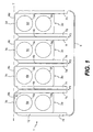
- Figure 1 shows a schematic cross sectional view of a first embodiment of a surface dielectric barrier discharge plasma unit 1 according to the invention.
- the unit 1 comprises an assembly of a multiple number of elongated shaped solid dielectric structure elements 2a, 2b, 2c, 2d.
- the elements 2a, 2b, 2c, 2d may be substantially arranged in parallel forming a solid dielectric structure such that an exterior treating surface 3a, 3b, 3c, 3d of each solid dielectric structure element 2a, 2b, 2c, 2d substantially extends in a common treating plane T.
- the elements 2a, 2b, 2c, 2d may be arranged so than respective exterior side surfaces of said elements are not exactly parallel to each other. This embodiment will be discussed in further detail with reference to Fig.
- inter spaces 4a, 4b, 4c between adjacent solid dielectric structure elements 2a, 2b, 2c, 2d define at least a part of gas flow paths P1, P2, P3 that extends along a surface of the solid dielectric structure elements 2a, 2b, 2c, 2d.
- the gas flow paths can have further sections as described below.
- Each solid dielectric structure element 2a, 2b, 2c, 2d is provided with an upper interior space 5a, 5b, 5c, 5d wherein an interior electrode 6a, 6b, 6c, 6d is arranged. Further, each solid dielectric structure element 2a, 2b, 2c, 2d comprises further, exterior electrodes 7a, 7b, 7c, 7d, 7e, 7f, 7g, 7h arranged adjacent to an exterior surface of the solid dielectric structure.
- the surface dielectric barrier discharge plasma unit 1 is arranged for operating at high gas pressures, e.g. at a gas pressures in the range 0,1-1 bar or significantly higher than atmospheric pressure, thereby enabling the treatment of a large gas volume and/or a large surface area.
- a structure to be treated is present substantially in the treating plane T.
- the structure to be treated is subjected to a specific plasma process, e.g. for surface activation, improvement of adhesion, dyability and printability, deposition by plasma-grafting, deposition by plasma polymerization and chemical bonding of particles to the structure to be treated.
- a specific plasma process e.g. for surface activation, improvement of adhesion, dyability and printability, deposition by plasma-grafting, deposition by plasma polymerization and chemical bonding of particles to the structure to be treated.
- the structure to be treated can be placed in the treating plane T for performing a batch process. Otherwise, the structure to be treated can be moved along the treating plane T, either substantially continuously, or intermittently.
- the multiple gas flow paths P1, P2, P3 gas particles can flow through the inter spaces 4 to the treating surfaces 3a, 3b, 3c, 3d at different locations, thereby rendering the plasma process more uniform and efficient.
- the thus defined gas flow paths P1, P2, P3 reaches the treating plane T at a multiple number of locations, so that the plasma process is performed even more uniformly.
- the plasma treating process is advantageously also performed more uniformly, thereby improving the treatment results and optionally reducing energy and chemical precursor gases that are needed for performing the plasma treatment.
- a relatively large treating surface 3a, 3b, 3c, 3d is obtained.
- the dielectric structure elements 2a, 2b, 2c, 2d have an elongated shape in a direction substantially transverse with respect to the cross sectional plane of Figure 1 .
- At least parts of the gas flow paths P1, P2, P3 run along exterior side surfaces 12 of the solid dielectric structure elements 2, the side surfaces 12 extending from the exterior treating surface 3.
- non-elongated shapes can be applied, e.g. substantially cubic shaped dielectric structures.
- the gas flow paths P1, P2, P3 running along the exterior side surfaces 12 are oriented substantially transverse with respect to the treating plane T wherein a structure to be treated by the unit 1 extends during operation of the unit 1.
- the gas flow paths P1, P2, P3 can be oriented substantially transverse with respect to a treating plane T wherein a structure to be treated by the unit 1 is moved in a treating direction along during operation of the unit 1.
- a part of the interspaces 4a, 4b, 4c can be used to transport treated gas away from the treating surface thereby further improving the uniformity and efficiency of the plasma treatment.
- the flow direction in a part of gas flow paths P1, P2, P3 is in the opposite direction. This option is particularly important when treating non or low gas permeable surfaces.
- the gas can be re-circulated after filtration and/or cooling.
- the inter spaces 4a, 4b, 4c are provided by defining a distance between exterior electrodes 7a, 7b, 7c, 7d, 7e, 7f, 7g, 7h that are adjacent with respect to each other.
- the above-mentioned distance can e.g. be defined by providing separate intermediate portions or by providing a non-flat outwardly oriented surface of the exterior electrodes, e.g. in a direction along the gas flow paths P1, P2, P3 and/or in a direction substantially transverse with respect to the cross sectional plane.
- the interior electrodes 6a, 6b, 6c, 6d are formed by an electrolyte, thus facilitating, apart from the electric functionality, a temperature conditioning means.
- the solid dielectric structure elements 2a, 2b, 2c, 2d can thus be cooled and/or heated.
- the electrolyte can be formed by a liquid and/or a gas. The conditioning of the plasma activated reactive gas in a specific temperature range can be very beneficial for treatments such as deposition at optimum reaction speed.
- the assembly Opposite to the treating plane T, the assembly is surrounded by a metal conducting structure 9, such as a metal cap, connected to the two most remote exterior electrodes. Consequently, high electric field values near edges of the exterior electrodes 7 that may lead to undesirable plasma formation in the flown gas in vicinity of those edges, is counteracted.
- a metal conducting structure 9 such as a metal cap
- the solid dielectric structure 2 comprises a multiple number of separate interior spaces, facilitating the production of the structure by an extrusion process. At least one of them may serve as a temperature conditioning fluid channel.
- the solid dielectric structure 2 might comprises an upper interior space 5a, 5b, 5c, 5d and a lower interior space 5e, 5f, 5g, 5h.
- a lower interior space can serve as an additional temperature conditioning channel.
- an interior space in the solid dielectric structure can serve as an electrode and/or a temperature conditioning fluid channel. It is noted here, however, that the structure 2 can also be provided with a single interior space that serves as an electrode and optionally as an temperature conditioning fluid channel.
- a cross section of the solid dielectric structure is not substantially square, it might be advantageous to provide more than one interior space in the structure, thereby balancing internal forces in the structures, so that production by extrusion is facilitated. Unacceptable, possible temperature depending, large stresses that may occur in the material during its manufacturing or application for plasma treatment, are counteracted.
- An additional interior space can be filled with an electrical isolator, such as a gas, transformer oil or a solid dielectric, such as epoxy. Otherwise, the additional interior space can serve as an electrode. By manipulating the voltage of the electrode in the additional interior space, e.g. by applying a voltage similar to that of exterior electrodes, the location of the surface plasma can in an advantageous way be controlled.
- a minimal distance between an exterior surface of the solid dielectric structure on the one hand and a brim of an interior space in the structure is determined by break through characteristics of the structure material and by a desire to electromagnetically couple the interior electrode and exterior (conducting) surface dielectric barrier plasma with a minimal electrical capacitance.
- This capacitance is a determining factor influencing the power surface density of the plasma [Watt/m 2 ].
- the above-mentioned minimal distance can as an example be chosen between approximately 0.5 mm and approximately 1 mm. However, also other distances can be applied, e.g. 2 mm or more, or 0.3 mm or less.
- the exterior electrodes 7 cover substantially the entire side surfaces 12 of the solid dielectric structure 2 at a location where the exterior electrodes 7, also called corona electrodes or sharp electrodes, and the treating surfaces 3 meet each other, the exterior electrodes 7 comprise a sharp end, thereby providing a well defined triple point between the solid dielectric structure 2, the exterior electrode and the gas induced via the gas flow paths. Since the exterior electrodes are positioned outside the treating plane T, a thickness of the exterior electrode can be chosen relatively large compared with a situation wherein the exterior electrodes are positioned at the treating surface 3 of the solid dielectric structure 2. Further, wear of the electrodes e.g.
- the arranging the exterior electrodes 7 at side surfaces due to friction forces exerted by materials of the structure to be treated is avoided by the arranging the exterior electrodes 7 at side surfaces. Further, erosion or corrosion of the exterior electrodes 7 can be suppressed by using relatively thick metal strips and by effective temperature control. Also, the life time of the exterior electrodes 7 is extended. It is noted that by arranging the exterior electrodes 7 such that they at least partially cover exterior surfaces of the solid dielectric structures 2, cooling of the structures 2 can be performed by the exterior electrodes 7, e.g. by connecting the exterior electrodes 7 to a cooling fin or heat sink. Further, cooling channels can be arranged inside the exterior electrodes 7.
- the solid dielectric structure 2 has been manufactured from a suitable dielectric material such as ceramic, e.g. specific types of alumina, glass or glass-ceramic materials.
- the adhesion between the dielectric material and the exterior electrodes can e.g. be realized by gluing the electrodes, e.g. using an epoxy resin.
- the gluing material is preferentially either having a high dielectric strength or having high conductivity in order to avoid electric breakdown of this material.
- the exterior electrode structure may have a U shape in which the solid dielectric structure is inserted.
- the exterior electrodes can be manufactured from metals such as stainless steel, high carbon steel, platinum or tungsten, coatings or alloys.
- the interior space 5 in the solid dielectric structure 2 is substantially elongated so that a relatively large treating surface 3 can be provided. Then, the interior space 5 forms a channel.
- the interior space 5 in the solid dielectric structure 2 has been manufactured by an extruding process, thereby providing a relatively simple, robust and cheap manufacturing method of a plasma unit 1 according to the invention.
- relatively long elongated interior spaces can be realized in solid dielectric structures, in particular structures having a single elongated interior space.
- up scaling to relatively large elements e.g. having a length of several meters is possible.
- the interior space can be manufactured by another process e.g. milling.
- the exterior electrodes 7 are in direct contact with the solid dielectric structure 2, so that the electric field is not merely dependent on the sharpness of the exterior electrodes, but is further enhanced by the permittivity difference between the gas and the solid dielectric structure 2.
- Scaling up electrodes for surface dielectric barrier plasma treatment may cause a relatively high electrical capacitive load.
- the electrical power delivered to each solid dielectric barrier structure is supplied by an individual power supply unit via its inner electrode 6 and the exterior electrode 7.
- the use of a separate power supply for each of those structures is beneficial for process control.
- groups of electrodes may be connected to separate power supplies.
- the exterior electrodes 7 of a single dielectric structure may be divided in segments where each segment receives electrical power from a separate power supply.
- the reduction of the electrical capacitance per power supply may be used to operate the surface barrier discharge when applying an alternating voltage potential between the electrodes at high frequency and/or with repetitive sharp rising pulses.
- the application of such pulses may result in a more uniform distribution of surface barrier discharge filaments along the treating surface.
- the costs of a modular power supply system can be reduced by using cheaper components.
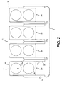
- Figure 2 shows a schematic cross sectional view of a second embodiment of a surface dielectric barrier discharge plasma unit 1 according to the invention.
- the exterior electrodes 7 partially cover exterior side surfaces 12 of the solid dielectric structure 2, thereby leaving upper sections of the exterior side surfaces uncovered.
- the region where the surface plasma is induced extends from the exterior treating surfaces 3 to the uncovered upper sections of the exterior side surfaces 12.
- the embodiment shown in Figure 2 allows for the treatment of a surface by means of plasma activated gas, i.e. the flow of gas via the gas flow paths P1, P2, P3 between the exterior electrodes 7, in combination with a, possibly other, gas that is fed along the treatment plane T of the unit 1.
- This type of so-called plasma jet is effective in case of high gas velocity since there is a short time between production of reactive particles in the plasma and their transport to the surface of a structure at a short distance.
- the partial decomposition (scissoring) of a precursor gas before deposition may be desirable.
- polymerization of a precursor gas, thereby forming sub-micron sized particles, is achieved before their deposition at the surface of the structure.
- FIG. 3 shows a schematic cross sectional view of a third embodiment of a surface dielectric barrier discharge plasma unit 1 according to the invention.
- the unit 1 comprises an electrically conducting, earthed and perforated plate 10 extending at least partially along an exterior treating surface 3 of the solid dielectric structure 2.
- the perforated plate 10 By providing the perforated plate 10 the distribution of the plasma activated gas is further improved. In this case it is preferred to apply a high gas speed, in order to limit loss of plasma reactivity by collisions between the reactive gas particles and between gas particles and the perforated plate before reaching the structure to be treated downstream. Further, a safer situation is obtained since the plate 10 is earthed. This option is advantageous when objects are treated in a space that is accessible for a person employing the plasma unit, e.g. for sterilization or disinfection purposes, such as floors, furniture, instruments or human skin.
- Figure 4a shows a schematic cross sectional view of a first solid dielectric structure 2 having an upper interior space 5a and a lower interior space 5e.
- the upper interior space 5a comprises a wall 11, e.g. implemented as an electrically conducting coating, foil or a tube.
- the space interior to the wall 11 is filled with a fluid, viz. a liquid or a gas 6 for conditioning the temperature of the solid dielectric structure 2.
- a fluid viz. a liquid or a gas 6
- Gas flow paths P1, P2 extends along side walls 12, the walls 12 extending from the treating surface 3.
- Figure 4b shows a schematic cross sectional view of a second solid dielectric structure 2 wherein the upper interior space 5a comprises a solid electrode 6, preferably centred in the middle of the upper interior space 5a.
- the electrode 6, which can be copper, is surrounded by an electrically conducting, temperature conditioning fluid 13 which can be an aqueous solution of a copper sulphate.
- Figure 4c shows a schematic cross sectional view of a third solid dielectric structure 2 wherein the upper interior space 5a is filled with an electrically conducting, temperature conditioning fluid 6.
- Figures 4b and 4c are superior over the embodiment shown in Figure 4a as inserting a solid metal rod or tube in extruded ceramic channels might be difficult due to unavoidable air inclusion causing localised plasma and resulting in thermal damage, and by because of the presence of small ceramic defects and/or protrusions.
- a solid dielectric structure 2 as shown in Figures 4a-c can be used for forming an assembly is shown in Figure 1 .
- a solid dielectric structure 2 can also be used separately.
- an elongated single solid dielectric structure 2 as shown in Figures 4a-c can be used for processing elongated objects, e.g. a plasma treatment of a fibre, a bundle of fibres or yarns.
- the gas flow paths P1, P2 are bounded by side surfaces 12 of the solid dielectric structure 2.
- the gas flow paths P1, P2 may further be bounded by further non-electrically conducting structures arranged adjacent the solid dielectric structure 2.
- an exterior electrode is connected to earth, thereby avoiding unsafe situations.
- the voltage differential between the interior and exterior electrode generates the surface dielectric barrier discharge plasma.
- the voltages can also be applied otherwise, e.g. by earthing the interior electrode and by applying the non-zero voltage to the exterior electrode.
- FIG. 5 shows a schematic cross sectional side view of a fourth embodiment of a surface dielectric barrier discharge plasma unit 1 according to the invention.
- an exterior treating surface 3 of the solid dielectric structure 2 is covered by a porous, electrically isolating layer 14.
- an individual solid dielectric structure 2 comprises three inner spaces 5a, 5e, 5i.
- a plasma unit 1 is obtained that is suitable for treating of a gas. Examples are removal of volatile organic compounds such as industrial solvents, hydrocarbons, CO, NOx, SO2, H2S, soot, dust and micro-organisms, e.g. in combustion gases, fuel conversion systems (e.g.
- the porous layer 14 comprises gas adsorbing materials e.g. porous alumina, zeolites for adsorbing gaseous pollutants and catalytic materials e.g. MnOx, Au/Ti02, for plasma-assisted chemical conversion.
- gas pollutants can be absorbed in the porous layer 14.
- the surface plasma 8 can be switched on and off periodically.
- pollutants are oxidized by means of plasma produced chemical species in the porous layer 14, mainly oxidative compounds such as O, O 3 , HO 2 , H 2 O 2 .
- an upper inner space 5a and a middle inner space 5e comprises electrodes while a lower inner space 5i comprises an isolator or an electrode having substantially the same potential as the exterior electrodes 7.
- Figures 6a-e shows a schematic cross sectional view of a fifth to a ninth embodiment, respectively of a surface dielectric barrier discharge plasma unit 1 according to the invention.
- a pair of solid dielectric structures 2a, 2b is shown each provided with a single interior space comprising an interior electrode 6a, 6b.
- a solid dielectric structure comprising one or more interior spaces can be manufactured easier and in a more robust way when exterior dimensions of the dielectric structure approach elongate shaped structures than plate shaped structures. Therefore, a solid dielectric structure approaching a square shaped form in cross sectional view can be realized in a relatively simple way.
- the structures 2a, 2b have different exterior electrode 7 configurations generating surface plasmas 8a, 8b at different locations along the exterior surface of the solid dielectric structures 2a, 2b.
- exterior electrodes at a first side of the solid structures, at an opposite side of the solid structures, at both sides of the solid structures and connected via a bridge 7e are shown.
- the injection of plasma activated gas, plasma jet can be combined with more localised produced plasma in close vicinity of the structure to be treated. Even different gases can be used along the structure to be treated and through the jet. By means of the applied voltages, the plasma can be more or less extended from the jet to the structure to be treated.
- a corona electrode having a gas permeable, saw tooth structure can be applied that is combined with a thinner, more flexible and well attached coating that will not erode because it does not carry the main current.
- Figure 7 shows a schematic perspective partially exploded view of the surface dielectric barrier discharge plasma unit 1 as shown in Fig. 1 .
- the assembly of solid dielectric structures 2a, 2b, ... , 2j having interior spaces 5, formed as channels, are positioned adjacent each other with the exterior electrodes 7 placed between them.
- Metal tubes 11 are pushed into the channels 5 and the entire assembly is placed over the metal cap 9 discussed above.
- the metal cap is provided with an entry 15 for flowing the gas towards the gas path sections along side surfaces of the solid dielectric structures.
- FIGS 8a, 8b, 8c show a schematic top view, cross sectional view and further cross sectional view, respectively, of the surface dielectric barrier discharge plasma unit 1 shown in Fig. 1 .
- Ends of the interior spaces 5 are coupled via a hose connection 18 or another coupling means to an electrolyte inlet channel 16 and electrolyte outlet channel 17, respectively.
- the electrolyte 6 serving as temperature conditioning fluid and electrode can flow from an inlet channel entrance En through the solid dielectric structure 2 towards an outlet channel exit Ex.
- the exterior electrodes 7 extend along distance W between a first plane A1 and a second plane A2 transversely with respect to a longitudinal axis of a interior space 5. Therefore, between the first plane A2 and the second plane A2 a plasma zone is defined.
- FIG. 9 shows a schematic cross sectional view of a tenth embodiment of a surface dielectric barrier discharge plasma unit 1 according to the invention.
- the unit 1 comprises a multiple number of solid dielectric structures 2 that are arranged in two shifted rows substantially parallel with respect to each other.
- the structures are formed as hollow tubes 2 filled with an electrolyte 6.
- the exterior surface of the tubes 2 is covered with a porous, electrically isolating layer 14, that is preferably gas adsorbent.
- the layer contains catalytic material.
- the tubes 2 are interconnected via an earthed exterior electrode 20, so that the exterior electrode 20 extends from a remote location into the porous, electrically isolating layer for generating in concert with the interior electrode 6 a surface dielectric barrier discharge plasma.
- the plasma unit 1 is provided with gas flow paths P1, P2, P3, P4 along exterior surfaces of the tubes 2.
- the plasma unit 1 can be operated periodically to chemically convert adsorbed gases. Further, the plasma unit 1 can be operated periodically to re-activate catalytic material.
- periodically operating the plasma means that the plasma process is discontinuous, interrupted, so that the plasma process is subsequently active and non-active. Alternatively, the plasma process is continuous or quasi continuous to continuously treating a structure to be treated.
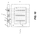
- Figures 10a and 10b show a schematic cross sectional view and a schematic top view, respectively, of a eleventh embodiment of a surface dielectric barrier discharge plasma unit 1 according to the invention.
- the solid dielectric structure 2 is substantially plate shaped and the structure is provided with a multiple number of slits 21 through which slits corresponding gas flow paths P1 extend.
- the unit 1 further comprises a single metal plate 7 serving as an exterior electrode and being located on top of the structure 2.
- the plate 7 is provided with slits that substantially correspond with the slits 21 of the solid dielectric structure 2. Again, multiple interior spaces 5, formed as channels, are provided in the dielectric structure 2.
- the channels can e.g. be manufactured by a milling or extrusion process.
- the channels comprise an interior electrode, implemented as an electrolyte so that the fluid can also serve as a temperature conditioning fluid.
- a surface plasma 8 is obtained.
- the surface plasma 8 is formed at the relatively sharp edges of the slits 21 in the metallic plate 7 and many plasma filaments can develop through the slits 21 in the solid dielectric structure 2 to an exterior surface of the structure 2 opposite to the metallic plate 7.
- the entire surface dielectric barrier discharge plasma unit 1 can be realized as a relatively light weight product.
- the plate-like solid dielectric structure can be formed integrally or by assembling solid dielectric structure elements, e.g. by joining them together by an epoxy or glass melt.
- a gas flow path that is oriented substantially transverse with respect to a treating surface of the solid dielectric structure can be realized through an opening in the solid dielectric structure, e.g. via a slit in an integral solid dielectric structure or via an inter space between solid dielectric structure elements that are arranged adjacent to each other in an assembly of solid dielectric structure elements forming a solid dielectric structure.
- the substantially transversely oriented gas flow path can be realized via a space exterior to the solid dielectric structure.
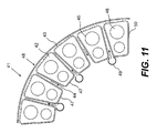
- Figure 11 shows a schematic cross sectional view of a twelfth embodiment of a surface dielectric barrier discharge plasma unit 41 according to the invention.
- the solid dielectric structures 42 are substantially arranged in parallel. However, the exterior side surfaces 50 of the structures 42 are not exactly parallel thereby providing a curved treating surface 43 which can be used to treat a flexible external structure 48.
- Interior spaces 45 are used to provide interior electrodes 46.
- the flow paths 44 between the exterior electrodes 47 are used to transport gases towards and from the treating surface 43.
- Gas injection tubes 49 are use to separate gas flows upstream and downstream from the plasma treatment zone.
- the gas injection tubes 49 may be either electrically insulating or electrically conducting. Conductive gas injection tubes may be used to electrically connect cables from a power supply to exterior electrodes 47.
- the embodiment shown in Figure 11 is particularly suitable for treatment of flexible materials which are transported from roll to roll, such as for example textile, polymeric foil or paper. Therefore a number of solid dielectric barrier structure elements can be arranged to form a cylinder which can be rotated so as to facilitate the continuous treatment of a flexible material.
- the shape of solid dielectric barrier structure elements can be such that the plasma treating surface 43 is at the inside of a cylindrical unit where it can be applied for the treatment of the external surface of cylinder shaped structures, e.g. tubes or hoses.
- any flat shaped structure can be treated at both sides by treatment of each side of that surface either simultaneously or in successive steps.
- the exterior electrodes 47 can be U shaped and connected to the dielectric structures 42 by means of a glue layer with either high dielectric strength or high electrical conductivity. In fig 11 the U shaped electrodes covers three sides of the solid dielectric structure.
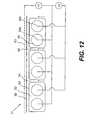
- Figure 12 shows a schematic cross sectional view of a thirteenth embodiment of a surface dielectric barrier discharge plasma unit 51 according to the invention.
- the solid dielectric structures 52 substantially arranged in parallel, have interior spaces 55 each serving as an interior electrode 56.
- a surface plasma is created along the treating surface 53 by application of an electric field between the interior electrodes 56a and 56b of each solid dielectric structure, thus without using an exterior electrode structure.
- plasma induced electrode erosion is avoided and the life time of the plasma treating unit is considerably increased.
- the gas flow paths 4 running along the exterior side surfaces 62 are oriented substantially transverse with respect to the treating plane wherein a structure 58 to be treated by the unit 51 extends.
- an additional perforated exterior electrode 63 can be placed opposite to the plasma treating surface 53.
- This option is particular useful for treating a relative thick gas permeable porous structure where the treatment by means of treating surface 53 alone would not be sufficient.
- an additional electric field between the perforated electrode 63 and the interior electrodes 56a and 56b the spatial structure of the surface dielectric barrier plasma can be enlarged from a relatively thin region along the treating surface 53 to a larger volume so as to obtain a deeper penetration of plasma in porous material 58.
- two power sources v1 and v2 may be used and operated at the same frequency but with adjustable amplitudes and/or relative phase shift.
- Figure 13 shows a schematic cross sectional view of a first plasma apparatus 22.
- the apparatus comprises four surface dielectric barrier discharge plasma units 1a, 1b, 1c, 1d according to an embodiment according to the invention as described above.
- the apparatus comprises a primary unit 1a, secondary units 1b, 1c and a tertiary unit 1d.
- a gas and/or a precursor is fed via an inlet 15 in a plasma unit 1a to split in a multiple number of gas flow paths P1, P2, P3, P4 along exterior electrodes 7 reaching a treating plane T.
- By applying voltages between exterior and interior electrodes 7, 5 surface plasmas are generated in the treating plane T, thus processing a structure to be treated 23.
- the plasma apparatus comprises rollers 24a, 24b and guiding means 25a, 25b for guiding the structure to be treated 23 along the plasma units 1a, 1b, 1c, 1d, in the treating plane T.
- the apparatus 22 also comprises a unit 26 for providing an additional gas mixture via an additional gas inlet 27 and/or for providing liquid aerosol particles via a nebuliser 29.
- the recirculating temperature controlled liquid is provided via inlet 28 and maintained via outlet 30 at a specific level suitable for ultrasonic nebulising.
- Figure 14 shows an additional schematic cross sectional view of the plasma apparatus 22 for illustrating the process in some more detail.
- the structure 23 to be treated is moving along the treating plane T in a treating direction TD.
- the structure passes the first plasma unit 1a for a surface discharge plasma pre-treatment, followed by a main plasma process via the secondary plasma units 1b, 1c.
- a plasma post treatment is performed by means of the tertiary plasma unit 1d.
- a gas is supplied to the treatment plane T.
- An aerosol containing gas is composed of a gas mixture (e.g.
- the liquid 31 e.g. styrene, may contain a suspension of solid sub-micron sized particles (e.g. SiO2 particles).
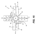
- Figure 15 shows a schematic cross sectional view of a second plasma apparatus 32 comprising an assembly of a multiple number of solid dielectric structures 2a, 2b, 2c, 2d.
- Treating surfaces 3a, 3b, 3c, 3d of the solid dielectric structures surround a treating volume 33. Further, the treating surfaces are curved so as to surround the treating volume 33.
- the solid dielectric structures comprise exterior side portions 34 extending from the treating surfaces 3 away from the treating volume 33 to enable a more or less homogeneous treatment and effective temperature conditioning.
- An inter space between exterior side surfaces of two adjacent solid dielectric structures defines at least partially gas flow paths P1, P2,P3, P4. During operation of the plasma apparatus 32 gas flows via the gas flow paths towards and from the treating volume 33.
- a structure to be treated is positioned, preferably a structure having an exterior periphery substantially coinciding with the shape of the treating surfaces 3 of the dielectric structures 2.
- the gas flow induce a pressure for keeping the structure to be treated in a desired position in the treating volume 33, e.g. in the centre of the treating volume 33 to avoid friction.
- bodies having a circular cross section, such as a fiber 34 can be treated by the plasma apparatus 32.
- the apparatus comprises two solid dielectric structures 2a, 2b; 2c, 2d being provided with a slit, an inter space, thus defining a gas flow path P2, P4.
- the solid dielectric structures 2a, 2b, 2c, 2d comprise inner spaces incorporating interior electrodes for generating a surface plasma.
- the configuration can also be designed such that more or less dielectric structures surround a treating volume, e.g. six dielectric structures.
- the plasma unit according to the invention can thus be used for several applications, such as for cleaning gas or treating surfaces of structures, e.g. for improvement of adhesion, dyability and printability, for layer deposition by plasma polymerization, layer deposition by plasma assisted grafting, particle deposition, sterilization or disinfection purposes.
- an interior electrode and a further, exterior electrode being arranged adjacent to an exterior surface of the solid dielectric structure for generating a surface dielectric barrier discharge plasma
- a pair of interior electrodes can be used for generating a surface plasma.
- the electrode can be placed in direct contact with the solid dielectric structure or adjacent thereto for generating a surface plasma.
- inventions described above comprise interior spaces that in cross sectional view are circular shaped. However, also other shapes can be applied, e.g. square shaped interior spaces.
Landscapes
- Physics & Mathematics (AREA)
- Engineering & Computer Science (AREA)
- Plasma & Fusion (AREA)
- Spectroscopy & Molecular Physics (AREA)
- Physical Or Chemical Processes And Apparatus (AREA)
- Plasma Technology (AREA)
Abstract
The invention relates to a surface dielectric barrier discharge plasma unit. The unit comprises a solid dielectric structure provided with an interior space wherein an interior electrode is arranged. Further, the unit comprises a further electrode for generating in concert with the interior electrode a surface dielectric barrier discharge plasma. The unit is also provided with a gas flow path along a surface of the structure.
Description
- The invention relates to a surface dielectric barrier discharge plasma unit comprising a solid dielectric structure provided with an interior space wherein an interior electrode is arranged, further comprising a further electrode for generating in concert with the interior electrode a surface dielectric barrier discharge plasma, wherein the plasma unit is further provided with a gas flow path along a surface of the structure.
- Solid dielectric structures having electrode structures arranged on or embedded in the dielectric structures are known for performing plasma processes. A first electrode is positioned on a treating surface of the structure, while a second electrode is placed on the opposite side of the dielectric structure. In such a process, gas flows needed for the plasma process can be induced along a treating surface of the structure.
- Dedicated plasma units having an interior electrode are also known. The interior electrode is obtained via a process wherein dielectric material is partially removed for forming a groove in a surface of the dielectric structure, an electrode deposition process and a process wherein the interior electrode is covered with dielectric material to obtain a flat dielectric surface. Again, a second electrode is placed on the opposite side of the dielectric structure. Dedicated plasma units having only interior electrodes are also known. By creating an electric field between pairs of interior electrodes a plasma process can be induced along a treating surface of the structure.
- However, plasma treatments appear to be non-uniform, especially when treating structures having low or non-gas permeable materials. The gas flow is flown in a plasma zone between the structure to be treated and a treating surface of the solid dielectric structure and reacts chemically and/or physically with the structure to be treated. As a consequence, less reactive gas particles are available in a desired area that is remote from and downstream to an area where the gas enters the plasma zone, thus resulting in a non-uniform plasma treatment. The composition of the plasma activated gas is changed during its passage along the treating structure. As a result the concentration of gaseous precursor gases or particles that are added to the plasma carrier gas, may be too high in the area where the gas enters the plasma zone and too low in the area where the gas leaves the plasma zone. A too high degree of precursor decomposition may result in unwanted precursor fragments that eventually cause decreased layer quality or undesirable dust by gas phase polymerization. As partial compensation of the change of precursor gas composition along the flow path in the plasma zone, generally a high gas flow rate is being applied resulting in a significant loss of unreacted precursor gas leaving the plasma zone.
- It is an object of the invention to provide a surface dielectric barrier discharge plasma unit according to the preamble, wherein the disadvantage identified above is reduced. In particular, the invention aims at obtaining a surface dielectric barrier discharge plasma unit according to the preamble enabling a more uniform and more efficient plasma treatment. Thereto, according to the invention, the gas flow path is oriented substantially transverse with respect to a treating surface of the solid dielectric structure.
- By orienting the gas flow path substantially transverse with respect to a treating surface of the structure, e.g. through or along a side surface of the solid dielectric structure, a desired plasma treating area near the treating surface of the structure can be reached directly by the gas flow. Accordingly, a gas flow path section upstream to the desired area but located in a plasma zone is reduced and the gas can be provided more evenly in the entire plasma region, so that a more uniform plasma process is enabled. Further, the gas particles are processed more efficiently.
- It is noted that the invention is partly based on the insight that a combination of an interior electrode and a further electrode can be used to counteract a surface plasma along the gas flow path section substantially transversely with respect to the treating surface of the solid dielectric surface, thereby enabling an efficient plasma process near the treating surface of the structure counteracting a plasma process with the gas particles before they reach the structure to be treated.
- Moreover, by the apparatus according to the invention, the apparatus can be scaled up to larger plasma zones, thereby improving a production volume.
- Further, by orienting the gas flow path substantially transverse with respect to the treating surface of the structure, the solid dielectric structure can be cooled efficiently by the gas flow, e.g. by flowing the gas along side surfaces of the structure or walls of the structure defining openings through which the gas can flow towards the plasma zone.
- Preferably, the interior electrode is implemented as an electrolyte, the electrolyte further serving as a temperature conditioning fluid, e.g. for efficiently cooling or heating the solid dielectric structure. In this way, conflicting requirements with respect to electrical isolation and heating guiding properties of the solid dielectric structure are elegantly circumvented. However, the electrolyte can also merely serve as interior electrode, e.g. if the temperature of the solid dielectric structure is conditioned otherwise.
- In an advantageous embodiment according to the invention, the interior space in the solid dielectric structure has been manufactured by an extruding process, thereby enabling an efficient manufacturing method of a plasma unit that can be scaled up relatively easily using standard extruding processes.
- The invention relates further to a method of generating a surface dielectric barrier discharge plasma.
- Other advantageous embodiments according to the invention are described in the following claims.
- By way of example only, embodiments of the present invention will now be described with reference to the accompanying figures in which
-
Fig. 1 shows a schematic cross sectional view of a first embodiment of a surface dielectric barrier discharge plasma unit according to the invention; -
Fig. 2 shows a schematic cross sectional view of a second embodiment of a surface dielectric barrier discharge plasma unit according to the invention; -
Fig. 3 shows a schematic cross sectional view of a third embodiment of a surface dielectric barrier discharge plasma unit according to the invention; -
Fig. 4a shows a schematic cross sectional view of a first solid dielectric structure; -
Fig. 4b shows a schematic cross sectional view of a second solid dielectric structure; -
Fig. 4c shows a schematic cross sectional view of a third solid dielectric structure; -
Fig. 5 shows a schematic cross sectional side view of a fourth embodiment of a surface dielectric barrier discharge plasma unit according to the invention; -
Fig. 6a shows a schematic cross sectional view of a fifth embodiment of a surface dielectric barrier discharge plasma unit according to the invention; -
Fig. 6b shows a schematic cross sectional view of a sixth embodiment of a surface dielectric barrier discharge plasma unit according to the invention; -
Fig. 6c shows a schematic cross sectional view of a seventh embodiment of a surface dielectric barrier discharge plasma unit according to the invention; -
Fig. 6d shows a schematic cross sectional view of a eighth embodiment of a surface dielectric barrier discharge plasma unit according to the invention; -
Fig. 6e shows a schematic cross sectional view of a ninth embodiment of a surface dielectric barrier discharge plasma unit according to the invention; -
Fig. 7 shows a schematic perspective partially exploded view of the surface dielectric barrier discharge plasma unit ofFig. 1 ; -
Fig. 8a shows a schematic top view of the surface dielectric barrier discharge plasma unit ofFig. 1 ; -
Fig. 8b shows a schematic cross sectional side view of the surface dielectric barrier discharge plasma unit ofFig. 8a ; -
Fig. 8c shows a further schematic cross sectional side view of the surface dielectric barrier discharge plasma unit ofFig. 8b ; -
Fig. 9 shows a schematic cross sectional view of a tenth embodiment of a surface dielectric barrier discharge plasma unit according to the invention. -
Fig. 10a shows a schematic cross sectional view of a eleventh embodiment of a surface dielectric barrier discharge plasma unit according to the invention; -
Fig. 10b shows a schematic top view of the surface dielectric barrier discharge plasma unit ofFig. 10a ; -
Fig.11 shows a schematic cross sectional view of a twelfth embodiment of a surface dielectric barrier discharge plasma unit according to the invention. -
Fig.12 shows a schematic cross sectional view of a thirteenth embodiment of a surface dielectric barrier discharge plasma unit according to the invention. -
Fig. 13 shows a schematic cross sectional view of a first plasma apparatus; -
Fig. 14 shows an additional schematic cross sectional view of the plasma apparatus ofFigure 11 ; and -
Fig. 15 shows a schematic cross sectional view of a second plasma apparatus. - It is noted that the figures show merely preferred embodiments according to the invention. In the figures, the same reference numbers refer to equal or corresponding parts.
-
Figure 1 shows a schematic cross sectional view of a first embodiment of a surface dielectric barrierdischarge plasma unit 1 according to the invention. Theunit 1 comprises an assembly of a multiple number of elongated shaped soliddielectric structure elements elements exterior treating surface dielectric structure element elements Fig. 11 . Further,inter spaces dielectric structure elements dielectric structure elements - Each solid
dielectric structure element interior space interior electrode dielectric structure element exterior electrodes discharge plasma unit 1 voltage differences are applied betweenexterior electrodes interior electrodes barrier discharge plasma dielectric structure elements interior electrodes plasmas - The surface dielectric barrier
discharge plasma unit 1 according to the invention is arranged for operating at high gas pressures, e.g. at a gas pressures in the range 0,1-1 bar or significantly higher than atmospheric pressure, thereby enabling the treatment of a large gas volume and/or a large surface area. - During operation of the
unit 1 a structure to be treated is present substantially in the treating plane T. By generating the plasma and by flowing gas to the treating plane T via the gas flow paths P1, P2, P3 the structure to be treated is subjected to a specific plasma process, e.g. for surface activation, improvement of adhesion, dyability and printability, deposition by plasma-grafting, deposition by plasma polymerization and chemical bonding of particles to the structure to be treated. In this manner, physical and/or chemical characteristics of a structure can be modified. It is noted that the structure to be treated can be placed in the treating plane T for performing a batch process. Otherwise, the structure to be treated can be moved along the treating plane T, either substantially continuously, or intermittently. By providing the multiple gas flow paths P1, P2, P3 gas particles can flow through the inter spaces 4 to the treatingsurfaces dielectric structure elements exterior treating surface inter spaces - By providing elongated shaped solid
dielectric structure elements surface dielectric structure elements Figure 1 . At least parts of the gas flow paths P1, P2, P3 run along exterior side surfaces 12 of the soliddielectric structure elements 2, the side surfaces 12 extending from theexterior treating surface 3. - Alternatively, also other, non-elongated shapes can be applied, e.g. substantially cubic shaped dielectric structures.
- The gas flow paths P1, P2, P3 running along the exterior side surfaces 12 are oriented substantially transverse with respect to the treating plane T wherein a structure to be treated by the
unit 1 extends during operation of theunit 1. Similarly, the gas flow paths P1, P2, P3 can be oriented substantially transverse with respect to a treating plane T wherein a structure to be treated by theunit 1 is moved in a treating direction along during operation of theunit 1. - Optionally, a part of the
interspaces - The
inter spaces exterior electrodes - The
interior electrodes dielectric structure elements - Opposite to the treating plane T, the assembly is surrounded by a
metal conducting structure 9, such as a metal cap, connected to the two most remote exterior electrodes. Consequently, high electric field values near edges of theexterior electrodes 7 that may lead to undesirable plasma formation in the flown gas in vicinity of those edges, is counteracted. - Optionally, the
solid dielectric structure 2 comprises a multiple number of separate interior spaces, facilitating the production of the structure by an extrusion process. At least one of them may serve as a temperature conditioning fluid channel. As shown inFigure 1 , thesolid dielectric structure 2 might comprises an upperinterior space interior space structure 2 can also be provided with a single interior space that serves as an electrode and optionally as an temperature conditioning fluid channel. - If a cross section of the solid dielectric structure is not substantially square, it might be advantageous to provide more than one interior space in the structure, thereby balancing internal forces in the structures, so that production by extrusion is facilitated. Unacceptable, possible temperature depending, large stresses that may occur in the material during its manufacturing or application for plasma treatment, are counteracted. An additional interior space can be filled with an electrical isolator, such as a gas, transformer oil or a solid dielectric, such as epoxy. Otherwise, the additional interior space can serve as an electrode. By manipulating the voltage of the electrode in the additional interior space, e.g. by applying a voltage similar to that of exterior electrodes, the location of the surface plasma can in an advantageous way be controlled.
- A minimal distance between an exterior surface of the solid dielectric structure on the one hand and a brim of an interior space in the structure is determined by break through characteristics of the structure material and by a desire to electromagnetically couple the interior electrode and exterior (conducting) surface dielectric barrier plasma with a minimal electrical capacitance. This capacitance is a determining factor influencing the power surface density of the plasma [Watt/m2]. In practice, the above-mentioned minimal distance can as an example be chosen between approximately 0.5 mm and approximately 1 mm. However, also other distances can be applied, e.g. 2 mm or more, or 0.3 mm or less.
- In the embodiment shown in
Figure 1 , theexterior electrodes 7 cover substantially the entire side surfaces 12 of thesolid dielectric structure 2 at a location where theexterior electrodes 7, also called corona electrodes or sharp electrodes, and the treatingsurfaces 3 meet each other, theexterior electrodes 7 comprise a sharp end, thereby providing a well defined triple point between thesolid dielectric structure 2, the exterior electrode and the gas induced via the gas flow paths. Since the exterior electrodes are positioned outside the treating plane T, a thickness of the exterior electrode can be chosen relatively large compared with a situation wherein the exterior electrodes are positioned at the treatingsurface 3 of thesolid dielectric structure 2. Further, wear of the electrodes e.g. due to friction forces exerted by materials of the structure to be treated is avoided by the arranging theexterior electrodes 7 at side surfaces. Further, erosion or corrosion of theexterior electrodes 7 can be suppressed by using relatively thick metal strips and by effective temperature control. Also, the life time of theexterior electrodes 7 is extended. It is noted that by arranging theexterior electrodes 7 such that they at least partially cover exterior surfaces of the soliddielectric structures 2, cooling of thestructures 2 can be performed by theexterior electrodes 7, e.g. by connecting theexterior electrodes 7 to a cooling fin or heat sink. Further, cooling channels can be arranged inside theexterior electrodes 7. - The
solid dielectric structure 2 has been manufactured from a suitable dielectric material such as ceramic, e.g. specific types of alumina, glass or glass-ceramic materials. The adhesion between the dielectric material and the exterior electrodes can e.g. be realized by gluing the electrodes, e.g. using an epoxy resin. The gluing material is preferentially either having a high dielectric strength or having high conductivity in order to avoid electric breakdown of this material. The exterior electrode structure may have a U shape in which the solid dielectric structure is inserted. The exterior electrodes can be manufactured from metals such as stainless steel, high carbon steel, platinum or tungsten, coatings or alloys. - Preferably, the
interior space 5 in thesolid dielectric structure 2 is substantially elongated so that a relatively large treatingsurface 3 can be provided. Then, theinterior space 5 forms a channel. - In an advantageous way, the
interior space 5 in thesolid dielectric structure 2 has been manufactured by an extruding process, thereby providing a relatively simple, robust and cheap manufacturing method of aplasma unit 1 according to the invention. As a further advantage, relatively long elongated interior spaces can be realized in solid dielectric structures, in particular structures having a single elongated interior space. Thus, up scaling to relatively large elements, e.g. having a length of several meters is possible. By applying an extruding process, a one piecesolid dielectric structure 2 can be obtained. Alternatively, when non-elongated solid dielectric structures are required, the interior space can be manufactured by another process e.g. milling. - The
exterior electrodes 7 are in direct contact with thesolid dielectric structure 2, so that the electric field is not merely dependent on the sharpness of the exterior electrodes, but is further enhanced by the permittivity difference between the gas and thesolid dielectric structure 2. - Scaling up electrodes for surface dielectric barrier plasma treatment may cause a relatively high electrical capacitive load. In an advantageous way, the electrical power delivered to each solid dielectric barrier structure is supplied by an individual power supply unit via its
inner electrode 6 and theexterior electrode 7. Above a specific length (typically 1-4 m) of the elongated dielectric barrier structures, the use of a separate power supply for each of those structures is beneficial for process control. Alternatively, from the total number ofexterior electrodes 7 being part of a plasma treating unit, groups of electrodes may be connected to separate power supplies. As a second alternative, theexterior electrodes 7 of a single dielectric structure may be divided in segments where each segment receives electrical power from a separate power supply. The reduction of the electrical capacitance per power supply may be used to operate the surface barrier discharge when applying an alternating voltage potential between the electrodes at high frequency and/or with repetitive sharp rising pulses. The application of such pulses may result in a more uniform distribution of surface barrier discharge filaments along the treating surface. Further, the costs of a modular power supply system can be reduced by using cheaper components. -
Figure 2 shows a schematic cross sectional view of a second embodiment of a surface dielectric barrierdischarge plasma unit 1 according to the invention. Theexterior electrodes 7 partially cover exterior side surfaces 12 of thesolid dielectric structure 2, thereby leaving upper sections of the exterior side surfaces uncovered. As a consequence, the region where the surface plasma is induced extends from theexterior treating surfaces 3 to the uncovered upper sections of the exterior side surfaces 12. The embodiment shown inFigure 2 allows for the treatment of a surface by means of plasma activated gas, i.e. the flow of gas via the gas flow paths P1, P2, P3 between theexterior electrodes 7, in combination with a, possibly other, gas that is fed along the treatment plane T of theunit 1. This type of so-called plasma jet is effective in case of high gas velocity since there is a short time between production of reactive particles in the plasma and their transport to the surface of a structure at a short distance. In particular applications the partial decomposition (scissoring) of a precursor gas before deposition may be desirable. In specific applications polymerization of a precursor gas, thereby forming sub-micron sized particles, is achieved before their deposition at the surface of the structure. In particular applications it may be preferred to use different gases along gas flow paths P1, P2 and P3, e.g. for surface activation, layer or particle deposition and curing or further cross-linking of this polymer layer. -
Figure 3 shows a schematic cross sectional view of a third embodiment of a surface dielectric barrierdischarge plasma unit 1 according to the invention. Theunit 1 comprises an electrically conducting, earthed andperforated plate 10 extending at least partially along anexterior treating surface 3 of thesolid dielectric structure 2. By providing theperforated plate 10 the distribution of the plasma activated gas is further improved. In this case it is preferred to apply a high gas speed, in order to limit loss of plasma reactivity by collisions between the reactive gas particles and between gas particles and the perforated plate before reaching the structure to be treated downstream. Further, a safer situation is obtained since theplate 10 is earthed. This option is advantageous when objects are treated in a space that is accessible for a person employing the plasma unit, e.g. for sterilization or disinfection purposes, such as floors, furniture, instruments or human skin. -
Figure 4a shows a schematic cross sectional view of a firstsolid dielectric structure 2 having an upperinterior space 5a and a lowerinterior space 5e. The upperinterior space 5a comprises awall 11, e.g. implemented as an electrically conducting coating, foil or a tube. The space interior to thewall 11 is filled with a fluid, viz. a liquid or agas 6 for conditioning the temperature of thesolid dielectric structure 2. By providing an electrically conductingwall 11 the temperature conditioning fluid enclosed by an electrical conductor is thus shielded from electromagnetic fields, thereby rendering any material composition more stable over time. Gas flow paths P1, P2 extends alongside walls 12, thewalls 12 extending from the treatingsurface 3. -
Figure 4b shows a schematic cross sectional view of a secondsolid dielectric structure 2 wherein the upperinterior space 5a comprises asolid electrode 6, preferably centred in the middle of the upperinterior space 5a. Theelectrode 6, which can be copper, is surrounded by an electrically conducting,temperature conditioning fluid 13 which can be an aqueous solution of a copper sulphate. - Further,
Figure 4c shows a schematic cross sectional view of a thirdsolid dielectric structure 2 wherein the upperinterior space 5a is filled with an electrically conducting,temperature conditioning fluid 6. By filling the interior space with an electrically conducting, temperature conditioning fluid the requirement of gas free contact between the interior electrode and the solid dielectric structure in order to avoid undesirable plasma formation has been fulfilled. Further, using a liquid electrolyte electrode, the problem associated with different temperature dependent expansion coefficients of metal and ceramic has been solved. Further, also the problem of a reduced life time of thin metal coatings due to thermal/chemical degradation has been solved. Moreover, the embodiments ofFigures 4b and 4c are superior over the embodiment shown inFigure 4a as inserting a solid metal rod or tube in extruded ceramic channels might be difficult due to unavoidable air inclusion causing localised plasma and resulting in thermal damage, and by because of the presence of small ceramic defects and/or protrusions. - It is noted that a
solid dielectric structure 2 as shown inFigures 4a-c can be used for forming an assembly is shown inFigure 1 . However, such asolid dielectric structure 2 can also be used separately. As an example, an elongated singlesolid dielectric structure 2 as shown inFigures 4a-c can be used for processing elongated objects, e.g. a plasma treatment of a fibre, a bundle of fibres or yarns. The gas flow paths P1, P2 are bounded byside surfaces 12 of thesolid dielectric structure 2. In case of a singlesolid dielectric structure 2, the gas flow paths P1, P2 may further be bounded by further non-electrically conducting structures arranged adjacent thesolid dielectric structure 2. - Preferably an exterior electrode is connected to earth, thereby avoiding unsafe situations. By applying non-zero voltages to interior electrodes, the voltage differential between the interior and exterior electrode generates the surface dielectric barrier discharge plasma. If desired, the voltages can also be applied otherwise, e.g. by earthing the interior electrode and by applying the non-zero voltage to the exterior electrode.
-
Figure 5 shows a schematic cross sectional side view of a fourth embodiment of a surface dielectric barrierdischarge plasma unit 1 according to the invention. Here, anexterior treating surface 3 of thesolid dielectric structure 2 is covered by a porous, electrically isolatinglayer 14. Further, an individualsolid dielectric structure 2 comprises threeinner spaces plasma unit 1 is obtained that is suitable for treating of a gas. Examples are removal of volatile organic compounds such as industrial solvents, hydrocarbons, CO, NOx, SO2, H2S, soot, dust and micro-organisms, e.g. in combustion gases, fuel conversion systems (e.g. fuel or biomass to hydrogen), air conditioning applications, air supply systems for large buildings, hospitals, military compounds etc. Preferably, theporous layer 14 comprises gas adsorbing materials e.g. porous alumina, zeolites for adsorbing gaseous pollutants and catalytic materials e.g. MnOx, Au/Ti02, for plasma-assisted chemical conversion. By cooling the channels, gas pollutants can be absorbed in theporous layer 14. During operation of theunit 1, thesurface plasma 8 can be switched on and off periodically. In a plasma active period, pollutants are oxidized by means of plasma produced chemical species in theporous layer 14, mainly oxidative compounds such as O, O3, HO2, H2O2. Due to a temperature increase, a part of the adsorbed species may be desorbed and oxidized in plasma activated gas downstream of theunit 1. In a practical embodiment, an upperinner space 5a and a middleinner space 5e comprises electrodes while a lowerinner space 5i comprises an isolator or an electrode having substantially the same potential as theexterior electrodes 7. -
Figures 6a-e shows a schematic cross sectional view of a fifth to a ninth embodiment, respectively of a surface dielectric barrierdischarge plasma unit 1 according to the invention. A pair of soliddielectric structures interior electrode structures exterior electrode 7 configurations generatingsurface plasmas dielectric structures bridge 7e are shown. - The injection of plasma activated gas, plasma jet, can be combined with more localised produced plasma in close vicinity of the structure to be treated. Even different gases can be used along the structure to be treated and through the jet. By means of the applied voltages, the plasma can be more or less extended from the jet to the structure to be treated.
- In order to avoid plasma occurring on parts of the solid dielectric structure, a corona electrode having a gas permeable, saw tooth structure, can be applied that is combined with a thinner, more flexible and well attached coating that will not erode because it does not carry the main current.
-
Figure 7 shows a schematic perspective partially exploded view of the surface dielectric barrierdischarge plasma unit 1 as shown inFig. 1 . The assembly of soliddielectric structures interior spaces 5, formed as channels, are positioned adjacent each other with theexterior electrodes 7 placed between them.Metal tubes 11 are pushed into thechannels 5 and the entire assembly is placed over themetal cap 9 discussed above. The metal cap is provided with anentry 15 for flowing the gas towards the gas path sections along side surfaces of the solid dielectric structures. -
Figures 8a, 8b, 8c show a schematic top view, cross sectional view and further cross sectional view, respectively, of the surface dielectric barrierdischarge plasma unit 1 shown inFig. 1 . Ends of theinterior spaces 5 are coupled via ahose connection 18 or another coupling means to anelectrolyte inlet channel 16 andelectrolyte outlet channel 17, respectively. In this way, theelectrolyte 6 serving as temperature conditioning fluid and electrode can flow from an inlet channel entrance En through thesolid dielectric structure 2 towards an outlet channel exit Ex. Theexterior electrodes 7 extend along distance W between a first plane A1 and a second plane A2 transversely with respect to a longitudinal axis of ainterior space 5. Therefore, between the first plane A2 and the second plane A2 a plasma zone is defined. -
Figure 9 shows a schematic cross sectional view of a tenth embodiment of a surface dielectric barrierdischarge plasma unit 1 according to the invention. Theunit 1 comprises a multiple number of soliddielectric structures 2 that are arranged in two shifted rows substantially parallel with respect to each other. The structures are formed ashollow tubes 2 filled with anelectrolyte 6. The exterior surface of thetubes 2 is covered with a porous, electrically isolatinglayer 14, that is preferably gas adsorbent. Optionally, the layer contains catalytic material. Thetubes 2 are interconnected via anearthed exterior electrode 20, so that theexterior electrode 20 extends from a remote location into the porous, electrically isolating layer for generating in concert with theinterior electrode 6 a surface dielectric barrier discharge plasma. Further, theplasma unit 1 is provided with gas flow paths P1, P2, P3, P4 along exterior surfaces of thetubes 2. Theplasma unit 1 can be operated periodically to chemically convert adsorbed gases. Further, theplasma unit 1 can be operated periodically to re-activate catalytic material. In this context, periodically operating the plasma means that the plasma process is discontinuous, interrupted, so that the plasma process is subsequently active and non-active. Alternatively, the plasma process is continuous or quasi continuous to continuously treating a structure to be treated. -
Figures 10a and 10b show a schematic cross sectional view and a schematic top view, respectively, of a eleventh embodiment of a surface dielectric barrierdischarge plasma unit 1 according to the invention. InFigure 10 , thesolid dielectric structure 2 is substantially plate shaped and the structure is provided with a multiple number ofslits 21 through which slits corresponding gas flow paths P1 extend. In principle, it also possible to apply a single slit in the plate shapedstructure 2. However, by applying a multiple number of slits the gas can be provided at thestructure 2 to be treated in a more uniform way. InFigures 10a and 10b , theunit 1 further comprises asingle metal plate 7 serving as an exterior electrode and being located on top of thestructure 2. Theplate 7 is provided with slits that substantially correspond with theslits 21 of thesolid dielectric structure 2. Again, multipleinterior spaces 5, formed as channels, are provided in thedielectric structure 2. The channels can e.g. be manufactured by a milling or extrusion process. The channels comprise an interior electrode, implemented as an electrolyte so that the fluid can also serve as a temperature conditioning fluid. By applying an electric voltage between exterior and interior electrodes, asurface plasma 8 is obtained. Thesurface plasma 8 is formed at the relatively sharp edges of theslits 21 in themetallic plate 7 and many plasma filaments can develop through theslits 21 in thesolid dielectric structure 2 to an exterior surface of thestructure 2 opposite to themetallic plate 7. The entire surface dielectric barrierdischarge plasma unit 1 can be realized as a relatively light weight product. The plate-like solid dielectric structure can be formed integrally or by assembling solid dielectric structure elements, e.g. by joining them together by an epoxy or glass melt. - Thus, a gas flow path that is oriented substantially transverse with respect to a treating surface of the solid dielectric structure can be realized through an opening in the solid dielectric structure, e.g. via a slit in an integral solid dielectric structure or via an inter space between solid dielectric structure elements that are arranged adjacent to each other in an assembly of solid dielectric structure elements forming a solid dielectric structure. Alternatively, the substantially transversely oriented gas flow path can be realized via a space exterior to the solid dielectric structure.
-
Figure 11 shows a schematic cross sectional view of a twelfth embodiment of a surface dielectric barrierdischarge plasma unit 41 according to the invention. The soliddielectric structures 42 are substantially arranged in parallel. However, the exterior side surfaces 50 of thestructures 42 are not exactly parallel thereby providing a curved treatingsurface 43 which can be used to treat a flexibleexternal structure 48.Interior spaces 45 are used to provideinterior electrodes 46. Theflow paths 44 between theexterior electrodes 47 are used to transport gases towards and from the treatingsurface 43.Gas injection tubes 49 are use to separate gas flows upstream and downstream from the plasma treatment zone. Thegas injection tubes 49 may be either electrically insulating or electrically conducting. Conductive gas injection tubes may be used to electrically connect cables from a power supply toexterior electrodes 47. - The embodiment shown in
Figure 11 is particularly suitable for treatment of flexible materials which are transported from roll to roll, such as for example textile, polymeric foil or paper. Therefore a number of solid dielectric barrier structure elements can be arranged to form a cylinder which can be rotated so as to facilitate the continuous treatment of a flexible material. - As an alternative the shape of solid dielectric barrier structure elements can be such that the
plasma treating surface 43 is at the inside of a cylindrical unit where it can be applied for the treatment of the external surface of cylinder shaped structures, e.g. tubes or hoses. - In general any flat shaped structure can be treated at both sides by treatment of each side of that surface either simultaneously or in successive steps. The
exterior electrodes 47 can be U shaped and connected to thedielectric structures 42 by means of a glue layer with either high dielectric strength or high electrical conductivity. Infig 11 the U shaped electrodes covers three sides of the solid dielectric structure. -
Figure 12 shows a schematic cross sectional view of a thirteenth embodiment of a surface dielectric barrierdischarge plasma unit 51 according to the invention. The soliddielectric structures 52, substantially arranged in parallel, haveinterior spaces 55 each serving as an interior electrode 56. A surface plasma is created along the treatingsurface 53 by application of an electric field between theinterior electrodes structure 58 to be treated by theunit 51 extends. - Alternatively an additional perforated
exterior electrode 63 can be placed opposite to theplasma treating surface 53. This option is particular useful for treating a relative thick gas permeable porous structure where the treatment by means of treatingsurface 53 alone would not be sufficient. By application of an additional electric field between theperforated electrode 63 and theinterior electrodes surface 53 to a larger volume so as to obtain a deeper penetration of plasma inporous material 58. In order to obtain an adjustable plasma power density and plasma volume, two power sources v1 and v2 may be used and operated at the same frequency but with adjustable amplitudes and/or relative phase shift. -
Figure 13 shows a schematic cross sectional view of afirst plasma apparatus 22. The apparatus comprises four surface dielectric barrierdischarge plasma units primary unit 1a,secondary units tertiary unit 1d. As an indicative example of theunits 1, a gas and/or a precursor is fed via aninlet 15 in aplasma unit 1a to split in a multiple number of gas flow paths P1, P2, P3, P4 alongexterior electrodes 7 reaching a treating plane T. By applying voltages between exterior andinterior electrodes rollers plasma units apparatus 22 also comprises aunit 26 for providing an additional gas mixture via anadditional gas inlet 27 and/or for providing liquid aerosol particles via anebuliser 29. The recirculating temperature controlled liquid is provided viainlet 28 and maintained viaoutlet 30 at a specific level suitable for ultrasonic nebulising. -
Figure 14 shows an additional schematic cross sectional view of theplasma apparatus 22 for illustrating the process in some more detail. During operation of theapparatus 22, thestructure 23 to be treated is moving along the treating plane T in a treating direction TD. In a first step, the structure passes thefirst plasma unit 1a for a surface discharge plasma pre-treatment, followed by a main plasma process via thesecondary plasma units tertiary plasma unit 1d. Via a main gas passage way G, also called plasma polymerization zone, between bothsecondary plasma units unit 26, and liquid aerosols provided viadroplet nebuliser 29. The liquid 31 e.g. styrene, may contain a suspension of solid sub-micron sized particles (e.g. SiO2 particles). -
Figure 15 shows a schematic cross sectional view of asecond plasma apparatus 32 comprising an assembly of a multiple number of soliddielectric structures surfaces volume 33. Further, the treating surfaces are curved so as to surround the treatingvolume 33. The solid dielectric structures compriseexterior side portions 34 extending from the treatingsurfaces 3 away from the treatingvolume 33 to enable a more or less homogeneous treatment and effective temperature conditioning. An inter space between exterior side surfaces of two adjacent solid dielectric structures defines at least partially gas flow paths P1, P2,P3, P4. During operation of theplasma apparatus 32 gas flows via the gas flow paths towards and from the treatingvolume 33. In the treating volume 33 a structure to be treated is positioned, preferably a structure having an exterior periphery substantially coinciding with the shape of the treatingsurfaces 3 of thedielectric structures 2. Optionally, the gas flow induce a pressure for keeping the structure to be treated in a desired position in the treatingvolume 33, e.g. in the centre of the treatingvolume 33 to avoid friction. As an example, bodies having a circular cross section, such as afiber 34, can be treated by theplasma apparatus 32. The apparatus comprises twosolid dielectric structures dielectric structures - It is noted that the configuration can also be designed such that more or less dielectric structures surround a treating volume, e.g. six dielectric structures.
- The plasma unit according to the invention can thus be used for several applications, such as for cleaning gas or treating surfaces of structures, e.g. for improvement of adhesion, dyability and printability, for layer deposition by plasma polymerization, layer deposition by plasma assisted grafting, particle deposition, sterilization or disinfection purposes.
- The invention is not restricted to the embodiments described herein. It will be understood that many variants are possible.
- Instead of using an interior electrode and a further, exterior electrode being arranged adjacent to an exterior surface of the solid dielectric structure for generating a surface dielectric barrier discharge plasma, also a pair of interior electrodes can be used for generating a surface plasma. Further, if an exterior electrode is used, the electrode can be placed in direct contact with the solid dielectric structure or adjacent thereto for generating a surface plasma.
- The embodiments described above comprise interior spaces that in cross sectional view are circular shaped. However, also other shapes can be applied, e.g. square shaped interior spaces.
- Other such variants will be obvious for the person skilled in the art and are considered to lie within the scope of the invention as formulated in the following claims.
Claims (21)
- A surface dielectric barrier discharge plasma unit comprising a solid dielectric structure provided with an interior space wherein an interior electrode is arranged, further comprising a further electrode for generating in concert with the interior electrode a surface dielectric barrier discharge plasma, wherein the plasma unit is further provided with a gas flow path along a surface of the structure and wherein the gas flow path is oriented substantially transverse with respect to a treating surface of the solid dielectric structure.
- A plasma unit according to claim 1, wherein the further electrode is arranged adjacent to an exterior surface of the solid dielectric structure.
- A plasma unit according to claim 1 or 2, wherein the interior electrode is implemented as an electrolyte.
- A plasma unit according to claim 3, wherein the electrolyte further serves as a temperature conditioning fluid.
- A plasma unit according to any of the previous claims, wherein the interior electrode is enclosed by an electrical conductor.
- A plasma unit according to any of the previous claims, wherein the solid dielectric structure substantially has an elongate shape having an exterior treating surface and an exterior side surface extending from the exterior treating surface along which side surface at least a part of the gas flow path is located.
- A plasma unit according to any of the previous claims, wherein the solid dielectric structure comprises an opening through which at least a part of the gas flow path extends.
- A plasma unit according to any of the previous claims, further comprising an assembly of a multiple number of solid dielectric structures substantially arranged in parallel such that an exterior treating surface of each solid dielectric structure substantially extends in a common treating plane and wherein an inter space between adjacent solid dielectric structures defines at least a part of the gas flow path.
- A plasma unit according to any of the claims 1-5, wherein the solid dielectric structure is substantially plate shaped, the structure being provided with a slit through which slit the gas flow path extends.
- A plasma unit according to claim 8, wherein the solid dielectric structure is provided with a multiple number of slits each of them defining at least a part of a gas flow path.
- A plasma unit according to any of the previous claims, wherein the interior space in the solid dielectric structure is substantially elongated.
- A plasma unit according to any of the previous claims, wherein the interior space in the solid dielectric structure has been manufactured by an extruding process.
- A plasma unit according to any of the previous claims, wherein the solid dielectric structure comprises a multiple number of separate interior spaces, at least one of them merely serving as a temperature conditioning fluid channel.
- A plasma unit according to any of the previous claims, wherein an exterior side surface of a solid dielectric surface is at least partially covered by an exterior electrode.
- A plasma unit according to any of the previous claims, wherein an exterior treating surface of the solid dielectric surface is at least partially covered by an exterior electrode.
- A plasma unit according to any of the previous claims, further comprising an electrically conducting, earthed and perforated plate extending at least partially along an exterior treating surface of the solid dielectric structure.
- A plasma unit according to any of the previous claims, wherein an exterior treating surface of the solid dielectric structure is covered by a gas adsorbing, porous, electrically isolating layer.
- A plasma unit according to any of the previous claims, wherein an exterior electrode is connected to earth.
- A plasma unit according to any of the previous claims, comprising a multiple number of solid dielectric structures wherein a solid dielectric structure forms an elongated hollow tube in which tube an electrode is arranged, wherein the exterior surface of the tube is covered by a porous, electrically isolating layer and wherein an exterior electrode extends from a remote location into the porous, electrically isolating layer.
- A plasma unit according to any of the previous claims, comprising an assembly of a multiple number of solid dielectric structures wherein treating surfaces of the solid dielectric structures surround a treating volume and wherein the gas flow path is at least partially defined by an inter space between exterior side surfaces of two adjacent solid dielectric structures.
- A method of generating a surface dielectric barrier discharge plasma, comprising applying a voltage between an interior electrode arranged in an interior space of a solid dielectric structure and a further electrode, further comprising inducing a gas flow along a gas flow path along a surface of the structure wherein the gas flow path is oriented substantially transverse with respect to a treating plane of a structure to be treated by the unit.
Priority Applications (8)
| Application Number | Priority Date | Filing Date | Title |
|---|---|---|---|
| EP07112805A EP2046101A1 (en) | 2007-07-19 | 2007-07-19 | A surface dielectric barrier discharge plasma unit and a method of generating a surface plasma |
| CN2007800517406A CN101611656B (en) | 2006-12-28 | 2007-12-28 | Surface dielectric barrier discharge plasma unit and method for generating surface plasmons |
| EP07851965.9A EP2105042B1 (en) | 2006-12-28 | 2007-12-28 | A surface dielectric barrier discharge plasma unit and a method of generating a surface plasma |
| PCT/NL2007/050707 WO2008082297A1 (en) | 2006-12-28 | 2007-12-28 | A surface dielectric barrier discharge plasma unit and a method of generating a surface plasma |
| CN201210382439.6A CN102892248B (en) | 2006-12-28 | 2007-12-28 | Surface dielectric barrier discharge plasma unit and the method producing surface plasma |
| JP2009543973A JP5654238B2 (en) | 2006-12-28 | 2007-12-28 | Surface dielectric barrier discharge plasma unit and method for generating surface plasma |
| US12/521,473 US9131595B2 (en) | 2006-12-28 | 2007-12-28 | Surface dielectric barrier discharge plasma unit and a method of generating a surface plasma |
| JP2014235694A JP2015092484A (en) | 2006-12-28 | 2014-11-20 | Surface dielectric barrier discharge plasma unit and method of generating surface plasma |
Applications Claiming Priority (1)
| Application Number | Priority Date | Filing Date | Title |
|---|---|---|---|
| EP07112805A EP2046101A1 (en) | 2007-07-19 | 2007-07-19 | A surface dielectric barrier discharge plasma unit and a method of generating a surface plasma |
Publications (1)
| Publication Number | Publication Date |
|---|---|
| EP2046101A1 true EP2046101A1 (en) | 2009-04-08 |
Family
ID=38658488
Family Applications (1)
| Application Number | Title | Priority Date | Filing Date |
|---|---|---|---|
| EP07112805A Withdrawn EP2046101A1 (en) | 2006-12-28 | 2007-07-19 | A surface dielectric barrier discharge plasma unit and a method of generating a surface plasma |
Country Status (1)
| Country | Link |
|---|---|
| EP (1) | EP2046101A1 (en) |
Cited By (1)
| Publication number | Priority date | Publication date | Assignee | Title |
|---|---|---|---|---|
| CN103329632A (en) * | 2011-02-08 | 2013-09-25 | 松下电器产业株式会社 | Plasma generator, cleaning and purifying device using the plasma generator, and small-sized electrical apparatus |
Citations (3)
| Publication number | Priority date | Publication date | Assignee | Title |
|---|---|---|---|---|
| US20060042545A1 (en) * | 2003-05-27 | 2006-03-02 | Tetsuji Shibata | Plasma treatment apparatus, method of producing reaction vessel for plasma generation, and plasma treatment method |
| US20060162741A1 (en) * | 2005-01-26 | 2006-07-27 | Cerionx, Inc. | Method and apparatus for cleaning and surface conditioning objects with plasma |
| US20060272673A1 (en) * | 2003-06-16 | 2006-12-07 | Cerionx, Inc. | Method and apparatus for cleaning and surface conditioning objects using plasma |
-
2007
- 2007-07-19 EP EP07112805A patent/EP2046101A1/en not_active Withdrawn
Patent Citations (3)
| Publication number | Priority date | Publication date | Assignee | Title |
|---|---|---|---|---|
| US20060042545A1 (en) * | 2003-05-27 | 2006-03-02 | Tetsuji Shibata | Plasma treatment apparatus, method of producing reaction vessel for plasma generation, and plasma treatment method |
| US20060272673A1 (en) * | 2003-06-16 | 2006-12-07 | Cerionx, Inc. | Method and apparatus for cleaning and surface conditioning objects using plasma |
| US20060162741A1 (en) * | 2005-01-26 | 2006-07-27 | Cerionx, Inc. | Method and apparatus for cleaning and surface conditioning objects with plasma |
Cited By (1)
| Publication number | Priority date | Publication date | Assignee | Title |
|---|---|---|---|---|
| CN103329632A (en) * | 2011-02-08 | 2013-09-25 | 松下电器产业株式会社 | Plasma generator, cleaning and purifying device using the plasma generator, and small-sized electrical apparatus |
Similar Documents
| Publication | Publication Date | Title |
|---|---|---|
| EP2105042B1 (en) | A surface dielectric barrier discharge plasma unit and a method of generating a surface plasma | |
| KR101839823B1 (en) | Modular microplasma microchannel reactor devices, miniature reactor modules and ozone generation devices | |
| EP2345312B1 (en) | Apparatus and method for treating an object by plasma | |
| EP3062017A1 (en) | Superheated steam processing device | |
| US8696996B2 (en) | Device and method for generating a barrier discharge in a gas flow | |
| US20160355400A1 (en) | Method for synthesizing organic matter and submerged plasma device | |
| US12262461B2 (en) | Methods and apparatus for decomposing constituent elements of fluids | |
| CN100411974C (en) | A kind of ozone generating method and ozone generating device | |
| CA2810095C (en) | Device and method for the treatment of a gaseous medium and use of the device for the treatment of a gaseous medium, liquid, solid, surface or any combination thereof | |
| CN105050304A (en) | U-shaped plate type dielectric-barrier-discharge-based low-temperature plasma reactor and reactive system | |
| WO2024192184A1 (en) | Methods and apparatus for generating atmospheric pressure, low temperature plasma with changing parameters | |
| US20030168009A1 (en) | Plasma processing within low-dimension cavities | |
| CN115636473B (en) | Water treatment device and method based on plasma | |
| US11032898B2 (en) | Modular plasma jet treatment system | |
| JP5645157B2 (en) | Plasma device | |
| CN2934209Y (en) | Ozone generating device | |
| KR20250006268A (en) | Method for ionization of fluids | |
| KR20250006278A (en) | Method for ionization of fluids | |
| JP2025517622A (en) | Device for ionizing a fluid | |
| Ağıral | Electron driven chemistry in microreactors |
Legal Events
| Date | Code | Title | Description |
|---|---|---|---|
| PUAI | Public reference made under article 153(3) epc to a published international application that has entered the european phase |
Free format text: ORIGINAL CODE: 0009012 |
|
| AK | Designated contracting states |
Kind code of ref document: A1 Designated state(s): AT BE BG CH CY CZ DE DK EE ES FI FR GB GR HU IE IS IT LI LT LU LV MC MT NL PL PT RO SE SI SK TR |
|
| AX | Request for extension of the european patent |
Extension state: AL BA HR MK RS |
|
| AKX | Designation fees paid | ||
| REG | Reference to a national code |
Ref country code: DE Ref legal event code: 8566 |
|
| STAA | Information on the status of an ep patent application or granted ep patent |
Free format text: STATUS: THE APPLICATION IS DEEMED TO BE WITHDRAWN |
|
| 18D | Application deemed to be withdrawn |
Effective date: 20091009 |