EP2045872A1 - Coupling device for transponder and smart card with such device - Google Patents
Coupling device for transponder and smart card with such device Download PDFInfo
- Publication number
- EP2045872A1 EP2045872A1 EP07117825A EP07117825A EP2045872A1 EP 2045872 A1 EP2045872 A1 EP 2045872A1 EP 07117825 A EP07117825 A EP 07117825A EP 07117825 A EP07117825 A EP 07117825A EP 2045872 A1 EP2045872 A1 EP 2045872A1
- Authority
- EP
- European Patent Office
- Prior art keywords
- spiral
- coupling device
- transponder
- coupling
- spirals
- Prior art date
- Legal status (The legal status is an assumption and is not a legal conclusion. Google has not performed a legal analysis and makes no representation as to the accuracy of the status listed.)
- Granted
Links
- 230000008878 coupling Effects 0.000 title claims abstract description 91
- 238000010168 coupling process Methods 0.000 title claims abstract description 91
- 238000005859 coupling reaction Methods 0.000 title claims abstract description 91
- 239000011295 pitch Substances 0.000 claims abstract description 41
- 230000001939 inductive effect Effects 0.000 claims abstract description 26
- 239000000758 substrate Substances 0.000 claims description 7
- 238000000926 separation method Methods 0.000 claims description 4
- 230000009977 dual effect Effects 0.000 claims description 3
- 239000012792 core layer Substances 0.000 claims description 2
- 238000004519 manufacturing process Methods 0.000 description 19
- 238000013461 design Methods 0.000 description 12
- 238000000034 method Methods 0.000 description 8
- 230000006854 communication Effects 0.000 description 6
- 238000004804 winding Methods 0.000 description 6
- 238000004891 communication Methods 0.000 description 5
- 238000005516 engineering process Methods 0.000 description 5
- 230000008569 process Effects 0.000 description 5
- 230000005540 biological transmission Effects 0.000 description 3
- 238000010586 diagram Methods 0.000 description 3
- 239000010410 layer Substances 0.000 description 3
- 239000003990 capacitor Substances 0.000 description 2
- 230000000694 effects Effects 0.000 description 2
- 238000005530 etching Methods 0.000 description 2
- 238000002955 isolation Methods 0.000 description 2
- 239000000463 material Substances 0.000 description 2
- 230000007246 mechanism Effects 0.000 description 2
- 238000007639 printing Methods 0.000 description 2
- RYGMFSIKBFXOCR-UHFFFAOYSA-N Copper Chemical compound [Cu] RYGMFSIKBFXOCR-UHFFFAOYSA-N 0.000 description 1
- 238000013459 approach Methods 0.000 description 1
- 230000008859 change Effects 0.000 description 1
- 239000004020 conductor Substances 0.000 description 1
- 229910052802 copper Inorganic materials 0.000 description 1
- 239000010949 copper Substances 0.000 description 1
- 230000003247 decreasing effect Effects 0.000 description 1
- 239000003989 dielectric material Substances 0.000 description 1
- 238000009713 electroplating Methods 0.000 description 1
- 238000007667 floating Methods 0.000 description 1
- 238000009413 insulation Methods 0.000 description 1
- 230000003993 interaction Effects 0.000 description 1
- 239000002184 metal Substances 0.000 description 1
- 229910052751 metal Inorganic materials 0.000 description 1
- 238000004806 packaging method and process Methods 0.000 description 1
- 238000007650 screen-printing Methods 0.000 description 1
- 238000009450 smart packaging Methods 0.000 description 1
- 238000012360 testing method Methods 0.000 description 1
Images

Classifications
-
- H—ELECTRICITY
- H01—ELECTRIC ELEMENTS
- H01Q—ANTENNAS, i.e. RADIO AERIALS
- H01Q1/00—Details of, or arrangements associated with, antennas
- H01Q1/12—Supports; Mounting means
- H01Q1/22—Supports; Mounting means by structural association with other equipment or articles
- H01Q1/2208—Supports; Mounting means by structural association with other equipment or articles associated with components used in interrogation type services, i.e. in systems for information exchange between an interrogator/reader and a tag/transponder, e.g. in Radio Frequency Identification [RFID] systems
- H01Q1/2225—Supports; Mounting means by structural association with other equipment or articles associated with components used in interrogation type services, i.e. in systems for information exchange between an interrogator/reader and a tag/transponder, e.g. in Radio Frequency Identification [RFID] systems used in active tags, i.e. provided with its own power source or in passive tags, i.e. deriving power from RF signal
-
- G—PHYSICS
- G06—COMPUTING; CALCULATING OR COUNTING
- G06K—GRAPHICAL DATA READING; PRESENTATION OF DATA; RECORD CARRIERS; HANDLING RECORD CARRIERS
- G06K7/00—Methods or arrangements for sensing record carriers, e.g. for reading patterns
- G06K7/10—Methods or arrangements for sensing record carriers, e.g. for reading patterns by electromagnetic radiation, e.g. optical sensing; by corpuscular radiation
- G06K7/10009—Methods or arrangements for sensing record carriers, e.g. for reading patterns by electromagnetic radiation, e.g. optical sensing; by corpuscular radiation sensing by radiation using wavelengths larger than 0.1 mm, e.g. radio-waves or microwaves
- G06K7/10158—Methods or arrangements for sensing record carriers, e.g. for reading patterns by electromagnetic radiation, e.g. optical sensing; by corpuscular radiation sensing by radiation using wavelengths larger than 0.1 mm, e.g. radio-waves or microwaves methods and means used by the interrogation device for reliably powering the wireless record carriers using an electromagnetic interrogation field
- G06K7/10178—Methods or arrangements for sensing record carriers, e.g. for reading patterns by electromagnetic radiation, e.g. optical sensing; by corpuscular radiation sensing by radiation using wavelengths larger than 0.1 mm, e.g. radio-waves or microwaves methods and means used by the interrogation device for reliably powering the wireless record carriers using an electromagnetic interrogation field including auxiliary means for focusing, repeating or boosting the electromagnetic interrogation field
Definitions
- the invention relates to a coupling device for a transponder device and to a smart card comprising a transponder device inductively coupled to a coupling device.
- the object of the invention is more particularly a coupling device that is easy to manufacture, in particular for contactless or dual-interface cards.
- a coupling device for transponder generally comprises a primary antenna configured for long range communication with an external RFID reader and a secondary antenna connected in series, wherein the secondary antenna is configured as such to be inductively coupled to an antenna of the transponder device.
- Inductive coupling also called magnetic, capacitive or reactive coupling
- inductive coupling is defined in contrast to direct electrical coupling by electrically conductive material.
- References in the present description to inductive, magnetic, capacitive or reactive coupling refer to a coupling that is predominantly or primarily inductive, magnetic, capacitive or reactive. It will be appreciated that a coupling that is primarily inductive may also include some capacitive coupling. Conversely, a coupling that is primarily capacitive may also include some inductive (magnetic) coupling as a secondary coupling mechanism. Systems using primarily inductive coupling are referred to herein as inductive coupling, and systems using primarily capacitive coupling are referred to herein as capacitive coupling.
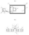
- FIG. 1 illustrates the disclosure made in US 5,955,723 .
- a transponder unit comprises a chip 1 with an antenna 2 and an inductive coupling device, comprising a primary antenna 3 and a secondary antenna 4 connected in series. All the elements are integrated in the card body and aim to extend the range and the quality of the communication of the transponder unit, in particular in the case of a non-contact card.
- a similar approach for RFID smart card is described in EP 0 931 295 .
- a module is provided with an antenna on the module, and the module is fixed in a recess of the card substrate accommodated with an inductive coupling device. The mounting is achieved in such a way that the antenna on the module is inductive coupled with the secondary antenna of the coupling device.
- Similar modules with antenna are disclosed in EP 0 875 039 and WO 07 026 077 . This solution is particularly interesting for dual (contact and non-contact) interface modules.
- a coupling device working with a transponder unit is proposed.
- the chip is electrically connected to the larger antenna (the primary antenna of the coupling device) without physical connection.
- Such units are much more resistant to mechanical stress than the ones using traditional connecting means such as pads, studs or wires.
- the antenna of the transponder is kept small (about the size of the chip or of the module) and is mounted on the same rigid structure as the chip. It can be the chip itself or in/on the chip packaging (as a chip module).
- the mechanism for generating the magnetic field in the magnetic coupling device may vary based on the antennas type or configuration. All types of coupling, at low frequency (LF: 30 - 300 kHz), high frequency (HF: 3 - 30 MHz) or ultra high frequency (UHF: over 300 MHz), are possible.
- LF low frequency
- HF high frequency
- UHF ultra high frequency
- the key issue of this technology is to find a simple and effective mass production process to manufacture the coupling device.
- the problem is that all elements of the coupling device have to be tuned accurately in order to obtain the desired transmission characteristic and performance of the whole system (coupling device + transponder device). This is illustrated for example in the equation giving the mutual inductance in EP 1 325 468 .
- One solution (use for example by Smart Packaging Solutions, France) is to use an etched antenna on a core sheet of dielectric material. Two extremities of the antenna, one on each side of the sheet, are enlarged to form the opposing electrode surface of a capacitor. By choosing accurately the two surface ratio, one can tune the capacitance of the element.
- a drawback of this method is that the antenna paths on each side of the sheet have to be connected electrically through the sheet.
- a simplified version of a coupling device is to use a conductive structure as resonator in order to increase the interaction of the transponder antenna with the magnetic field of the reader.
- a resonator can have different effects, and different forms.
- the loading bar described in US 6,285,342 is selectively adjusted to change the real part of the input impedance of a meander antenna.
- a spiral resonator which is coupled with the loop antenna of a transponder.
- the spiral is formed by a metallic wire of diameter d.
- the size of the pitch (mean distance between the turns of the spiral) p should be of 1 to 5d in order to ensure a proper magnetic coupling with the loop antenna.
- spiral winding is formed by a conductive path obtained by copper engraving.
- the path has a width of 0,15 mm.
- the pitch of the spiral winding is also of 0,15 mm, as the distance between the coil of the antenna (of the transponder to be coupled to the resonator) and one (internal / external) turn of the spiral.
- the extremities of the spiral winding are loose and there are the stray capacitances between the turns of the spiral, current resonance can occur at a particular frequency. This current is then transmitted to the coil of the antenna also by capacitive coupling.
- the two spiral resonators described in these last examples show mainly a capacitive coupling behavior. No inductive coupling with the antenna of a transponder is possible as the effect of the stray capacities are too important.
- a similar spiral resonator 5 is described in Fig. 2 .
- the conductive path forms a spiral with loose ends.
- Reference herein to spiral refers to a continuous path that follows a winding course (geometrically around a point, a form or a shape) and that show a plurality of spaced turns. In the example shown here, the spiral has a rectangular geometry , but any other geometries are possible.
- the distance between the turns On the electrical level, the most important parameter of such a resonator, beside the total length and the number of turns, is the distance between the turns.
- the mean distance between the turns of a spiral is herein called the pitch p of the spiral. If the pitch is small enough, stray capacitances 6 are created between different segments of the spiral that are parallel and close to each other. This is illustrated by the close view of Fig. 2 , on the side of which one has also added the equivalent electrical diagram of this segment of the resonator circuit. As the extremities of the spiral windings are loose and there are stray capacitances between the turns of the spiral, the spiral acts like a transmission line in which a current resonance occurs at a particular frequency.
- the stray capacitance diminishes very fast as the pitch increase.Being over 5 to 10 times the width of the conductive path, the stray capacitance becomes negligible.
- pitch as defined herein supposes regular spiral geometry with a constant winding increasing step. In reality, design and manufacturing constraint make impossible to create a perfectly constant interturn distance. Therefore, the definition of pitch herein has to be understood as the mean interturn distance of the whole spiral (weighted on the length of the spiral).
- the coupling device is formed by a continuous conductive path having a central section and two extremity sections, the central section forming at least a small spiral for inductive coupling with the transponder device, the extremity sections forming each one large spiral for inductive coupling with the reader device, wherein the small spiral shows a larger pitch than the ones of the large spirals, and wherein the two extremities of the continuous path are loose such a way that the coupling device forms an open circuit.
- the pitches of the large spirals are chosen so that interturn stray capacitances are considerable and that the large spirals have mainly a capacitive behaviour.
- the pitch of the small spiral is chosen so that the interturn stray capacitances are negligible, and that the small spiral has mainly an inductive behaviour.
- the fundamental idea of the invention is to use the interturn stray capacitances of the "primary antenna" of the coupling device to optimize the communication with the reader device, when the "secondary antenna” shows a mainly inductive behaviour that is suitable for the inductive coupling to the transponder unit.
- the manufacturing of the coupling device is therefore reduced to the manufacturing of a single continuous conductive path, but with a complex design.
- the design parameters are multiple: total antenna length, number of turn, dimensions, geometry, relative positioning, pitches, etc. All these design parameters are totally interdependent and their accurate determination is a complex empirical process. It has to be considered as a whole complex system interacting with the transponder unit in order to communicate optimally with an external reader.
- the continuous conductive path is made by a conductive wire embedded on the surface of a substrate.
- a conductive wire assures that the electrical and magnetical characteristics are constant and homogeneous all along the whole conductive path.
- Wire embedding is a fast, effective and well known manufacturing process. It is easy to program embedding heads for complex design achievement. Elements like small pitches or bridges (in particular if an insulated wire is used) are easy to achieve, even under mass production conditions (fast, reliable, reproducible, high quality and high yield).
- the substrate can be a core layer for a smart card, that can be laminated with the transponder unit in the body of the card.
- a particular embodiment is to use the coupling device in relationship with a dual interface module, presenting contact pads at the surface of the card for a contact-type communication and an antenna integrated in the module in order to be coupled to the coupling device for a contactless-type communication.
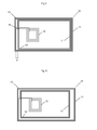
- FIG 3 shows a first embodiment of the coupling device 10 of the invention.
- Such device is used to couple a transponder device 7 (represented here next to the coupling unit 10) with an external reader device not represented in this figure.
- the coupling device 10 is formed by a single conductive path having a central section and two external sections.
- the central portion is formed as a small spiral 12 with a large pitch, whereas the two external sections form a large spiral 11 and 11' with a small pitch.
- the spiral 11 and 11' are two distinct spiral physical elements, but forming a single geometrical spiral element (with a short interruption in the middle).
- the path forms first almost four turns of a large spiral 11 with a small pitch.
- This geometrical element is then stopped and the path extends then in the central region of the spiral 11 to form there a smaller spiral 12 of three turns and with a larger pitch.
- this geometrical element is stopped, and the conductive path goes back just next to the first interruption point.
- the path forms a second large spiral 11', which is the geometrical continuation of the large spiral 11, with also almost four turns and approximately the same small pitch.
- the distance of separation between the internal turn of the large spiral 11 and the external turn of the large spiral 11' is constant and equal to the pitch of the large spirals.
- the continuous path comprises also some small link portions, like the ones between the different bridges 14.
- the extremities 13 and 13' of the continuous path are also geometrically not part of the large spirals 11 and 11', but are formed as small free extensions of them. As long as they stay loose or do not form an additional radiating element, the exact form of these extremities is not relevant for the invention.
- the continuous conductive path there are many ways to manufacture the continuous conductive path, such as for example: printing (by screen printing, ink-jet etc.), etching (plasma, electro-plating), fixed (conductive band or metal surface, or wire for example), ...
- the preferred embodiment according the invention is to use a conductive wire, preferably embedded on an substrate.
- a conductive wire ensures that the electrical and magnetic characteristics are constant and homogeneous all along the whole conductive path.
- Wire embedding is a fast, effective and well known manufacturing process. It is easy to program embedding heads for a complex design achievement.
- the continuous path is made by an insulated wire that has been embedded on a substrate (not shown).
- an insulated wire it is extremely advantageous to form bridge 14 along the path. Due to the complexity of the design (different spiral structures), one cannot avoid the use of bridge, where a path portion is crossing over (or under) another path portion.
- the creation of a bridge portion is only possible by interrupting the manufacturing process of the conductive path, covering the bridged path portion with an isolation material, and restarting the manufacturing of the conductive path by forming a path portion over the isolation material.
- Such interruption, in the process and in the structure of the conductive path is considered a drawback. Therefore an advantageous embodiment is to use an insulated wire.
- the insulation of the wire ensures that no short circuit will occur.
- An alternative is to use non insulated wire and the process step described in DE 19 916 180 .
- the transponder device 7 represented next to the coupling device 10 on Fig. 3 is intended to be placed over the small spiral 12 (as shown by the arrow) in order to be coupled to the coupling device 10.
- the transponder device has an antenna 8 connected to a transponder chip 9 (integrated circuit). Any kind of transponder device can be used.
- the general idea is to use a small compact transponder device as for example coil-on-chip (as in EP 0 977 145 ), module with antenna (as in EP 0 875 039 and WO 07 026 077 ), air-bobbin (thin wire wound as a small annular (with some hundreds of turns: LF type) and directly bonded on the pads of the chip, as in EP 0 756 736 ).
- the transponder device 7 represented in figure 3 is purely symbolic, and neither the design of the antenna 8, nor its connection to the chip 9 should be understood as limiting the scope of the invention.
- the geometry and dimensions of the antenna 8 must be as similar as possible to the ones of the spiral 12.
- the leads of the coils should extend at the slightest possible spacing from one another in order to couple inductively well. It doesn't mean that the design of the antenna 8 and of the spiral 12 should be absolutely identical.
- the design of the spiral 12 is submitted to different constraints than the transponder antenna: available space on the substrate, large pitch, diameter of the wire, etc. The more portions of the spiral 12 are parallel and close to portions of the antenna 8, the better the inductive coupling. Both elements can have differences like: physical nature (wire, printed, deposited, ...), number of turns, pitch, ...
- the small spiral 12 can also extend externally to the large spirals 11 and 11'. It all depends on the available surface.
- FIG 4 shows a simplified theoretical electrical diagram equivalent to the embodiment shown in figure 3 .
- the two large spirals 11 and 11' are represented by the discrete succession of local interturn stray capacitances and local path portions impedances, as discussed above in the description of Fig. 2 .
- the two spirals 11 and 11' act like a transmission line in which a current resonance occurs at a particular frequency. This current also circulates in the coil portion (small spiral) 12 facing directly the antenna 8, and an inductively generated corresponding current is generated in the transponder 7.
- a RFID communication process can be achieved between an external RFID reader and the transponder chip 9, via the resonance current occurring in the large spirals 11 and 11'.
- the determination of the design parameters is an empirical process.
- One is facing a complex system with interdependent parameters.
- the two large spirals 11 and 11' as represented in the Fig. 3 are coupled together, as there are at least additional stray capacitances between them.
- These additional coupling capacities 15 have been added (on a hypothetical basis) in gray doted lines in the Fig. 4 .
- the complete real equivalent electrical diagram of Fig. 3 is even more complex but the principles are illustrated in the present application.
- the geometry and dimensions of the antenna 8 must be as similar as possible to the ones of the spiral 12.(as discussed above).
- a pitch of the small spiral 12 approximately equivalent to the fifth or ten times the diameter of the wire used to form the conductive path has shown to be a good and practical solution.
- the two large spirals 11 and 11' should be as similar as possible.
- the more equivalent their electrical (and magnetical) properties the better the current resonance and the better the performances of the coupling device.
- the two spirals should be perfectly symmetrical, positioned one next to the other. But due to space constraint, this will often not be possible.
- the embodiment of Fig. 3 is an example of a practical solution. Any variation has to be understood as being part of the scope of this invention.
- Figures 5 and 6 show two further embodiments of the coupling device 10 of the invention.
- the two large spirals 11 and 11' show a distance of separation d that is much larger than their pitch.
- this gap exist only on one side of the perimeter of the respective large spirals, whereas on the other side, the distance of separation between the internal turn of the large spiral 11 and the external turn of the large spiral 11' is constant and equal to the pitch of the large spirals.
- Embodiment of Fig 6 . is even more extreme, as it shows different gaps (each much larger than the pitch of the large spirals) for each side of the large spirals 11 and 11'.
- a resonator as illustrated on Fig. 2 .
- the coupling device 10 according the Fig. 5 has been manufactured by wire embedding on a PVC layer.
- a spiral resonator is manufactured also by wire embedding.
- This resonator has the same geometry and dimensions as the external large spiral 11.
- This spiral resonator can eventually have more turns (the number of turns must be chosen accurately with the desired resonant frequency) and has two loose ends.
- the two layers are then laminated together (eventually in a card body).
Abstract
Description
- The invention relates to a coupling device for a transponder device and to a smart card comprising a transponder device inductively coupled to a coupling device. The object of the invention is more particularly a coupling device that is easy to manufacture, in particular for contactless or dual-interface cards.
- The technology of an inductive coupling unit is known in the art and was first published for RFID transponders in
US 5,270,717 , as a solution to provide an extended range transponder/antenna configuration. A standard transponder is coupled to a long and narrow antenna by a loosely coupled coil. This document describes the general principle of a inductive coupling device. - A coupling device for transponder generally comprises a primary antenna configured for long range communication with an external RFID reader and a secondary antenna connected in series, wherein the secondary antenna is configured as such to be inductively coupled to an antenna of the transponder device.
- Inductive coupling, also called magnetic, capacitive or reactive coupling, is defined in contrast to direct electrical coupling by electrically conductive material. References in the present description to inductive, magnetic, capacitive or reactive coupling refer to a coupling that is predominantly or primarily inductive, magnetic, capacitive or reactive. It will be appreciated that a coupling that is primarily inductive may also include some capacitive coupling. Conversely, a coupling that is primarily capacitive may also include some inductive (magnetic) coupling as a secondary coupling mechanism. Systems using primarily inductive coupling are referred to herein as inductive coupling, and systems using primarily capacitive coupling are referred to herein as capacitive coupling.
- This technology has been extensively used for manufacturing non-contact cards. As an example,
figure 1 illustrates the disclosure made inUS 5,955,723 . A transponder unit comprises achip 1 with anantenna 2 and an inductive coupling device, comprising aprimary antenna 3 and asecondary antenna 4 connected in series. All the elements are integrated in the card body and aim to extend the range and the quality of the communication of the transponder unit, in particular in the case of a non-contact card. - A similar approach for RFID smart card is described in
EP 0 931 295 . A module is provided with an antenna on the module, and the module is fixed in a recess of the card substrate accommodated with an inductive coupling device. The mounting is achieved in such a way that the antenna on the module is inductive coupled with the secondary antenna of the coupling device. Similar modules with antenna are disclosed inEP 0 875 039 andWO 07 026 077 - An alternative is presented in
EP 0 977 145 , where an antenna is formed directly on the surface of the chip, when the primary and secondary antennas of the coupling device are formed on a module board on which the chip is going to be mounted by the flip-chip method. This kind of small transponders (chip and antenna together) is called coil-on-chip and is known in the art and largely distributed on the market. - In all the documents of the prior art cited above, a coupling device working with a transponder unit is proposed. The chip is electrically connected to the larger antenna (the primary antenna of the coupling device) without physical connection. Such units are much more resistant to mechanical stress than the ones using traditional connecting means such as pads, studs or wires. The antenna of the transponder is kept small (about the size of the chip or of the module) and is mounted on the same rigid structure as the chip. It can be the chip itself or in/on the chip packaging (as a chip module).
- All configurations disclosed above, also as dipole, patch, slot, spiral, wire, single-loop, multi-loops and various hybrid antenna types are suitable for such inductive coupling systems. The mechanism for generating the magnetic field in the magnetic coupling device may vary based on the antennas type or configuration. All types of coupling, at low frequency (LF: 30 - 300 kHz), high frequency (HF: 3 - 30 MHz) or ultra high frequency (UHF: over 300 MHz), are possible.
- The key issue of this technology is to find a simple and effective mass production process to manufacture the coupling device. The problem is that all elements of the coupling device have to be tuned accurately in order to obtain the desired transmission characteristic and performance of the whole system (coupling device + transponder device). This is illustrated for example in the equation giving the mutual inductance in
EP 1 325 468 - Many solutions are proposed today that all involve a multiple step manufacturing process.
- One solution (use for example by Smart Packaging Solutions, France) is to use an etched antenna on a core sheet of dielectric material. Two extremities of the antenna, one on each side of the sheet, are enlarged to form the opposing electrode surface of a capacitor. By choosing accurately the two surface ratio, one can tune the capacitance of the element. A drawback of this method is that the antenna paths on each side of the sheet have to be connected electrically through the sheet.
- Other solutions like connecting capacitors, closing antenna loops, etc... all imply additional manufacturing steps, most of the time with high technical difficulties and error potential. This complexity implies lower reproducible and quality yield that are essential drawbacks for mass production.
- A simplified version of a coupling device is to use a conductive structure as resonator in order to increase the interaction of the transponder antenna with the magnetic field of the reader. Such a resonator can have different effects, and different forms. For example, the loading bar described in
US 6,285,342 is selectively adjusted to change the real part of the input impedance of a meander antenna. - In
DE 100 10 936 , a spiral resonator is described which is coupled with the loop antenna of a transponder. The spiral is formed by a metallic wire of diameter d. The size of the pitch (mean distance between the turns of the spiral) p should be of 1 to 5d in order to ensure a proper magnetic coupling with the loop antenna. - Another spiral resonator is disclosed in
WO 06 125 916 - By contrast to the coupling device described above, the two spiral resonators described in these last examples show mainly a capacitive coupling behavior. No inductive coupling with the antenna of a transponder is possible as the effect of the stray capacities are too important. A similar
spiral resonator 5 is described inFig. 2 . The conductive path forms a spiral with loose ends. Reference herein to spiral refers to a continuous path that follows a winding course (geometrically around a point, a form or a shape) and that show a plurality of spaced turns. In the example shown here, the spiral has a rectangular geometry , but any other geometries are possible. - On the electrical level, the most important parameter of such a resonator, beside the total length and the number of turns, is the distance between the turns. The mean distance between the turns of a spiral is herein called the pitch p of the spiral. If the pitch is small enough,
stray capacitances 6 are created between different segments of the spiral that are parallel and close to each other. This is illustrated by the close view ofFig. 2 , on the side of which one has also added the equivalent electrical diagram of this segment of the resonator circuit. As the extremities of the spiral windings are loose and there are stray capacitances between the turns of the spiral, the spiral acts like a transmission line in which a current resonance occurs at a particular frequency. The smaller the pitch, the stronger the interturn stray capacitances and the stronger the resonance. The stray capacitance diminishes very fast as the pitch increase.Being over 5 to 10 times the width of the conductive path, the stray capacitance becomes negligible. - The pitch as defined herein supposes regular spiral geometry with a constant winding increasing step. In reality, design and manufacturing constraint make impossible to create a perfectly constant interturn distance. Therefore, the definition of pitch herein has to be understood as the mean interturn distance of the whole spiral (weighted on the length of the spiral).
- Of interest is also the document
WO 07 025 934 - It is an aim of the present invention to improve the known devices.
- More specifically, it is a aim of the present invention to provide a coupling device for a transponder device that is easy to manufacture, in particular for contactless or dual-interface cards.
- It is a further aim of the present invention to provide a coupling device for which the manufacturing process is simple to carry out, reliable and which produces devices of good quality, in particular by using one single manufacturing step, implying only one element and one technology and by avoiding the use of multiple electrical elements to be connected.
- According to the present invention, the coupling device is formed by a continuous conductive path having a central section and two extremity sections, the central section forming at least a small spiral for inductive coupling with the transponder device, the extremity sections forming each one large spiral for inductive coupling with the reader device, wherein the small spiral shows a larger pitch than the ones of the large spirals, and wherein the two extremities of the continuous path are loose such a way that the coupling device forms an open circuit.
- The pitches of the large spirals are chosen so that interturn stray capacitances are considerable and that the large spirals have mainly a capacitive behaviour. And the pitch of the small spiral is chosen so that the interturn stray capacitances are negligible, and that the small spiral has mainly an inductive behaviour.
- The fundamental idea of the invention is to use the interturn stray capacitances of the "primary antenna" of the coupling device to optimize the communication with the reader device, when the "secondary antenna" shows a mainly inductive behaviour that is suitable for the inductive coupling to the transponder unit.
- The manufacturing of the coupling device is therefore reduced to the manufacturing of a single continuous conductive path, but with a complex design. The design parameters are multiple: total antenna length, number of turn, dimensions, geometry, relative positioning, pitches, etc. All these design parameters are totally interdependent and their accurate determination is a complex empirical process. It has to be considered as a whole complex system interacting with the transponder unit in order to communicate optimally with an external reader.
- In a preferred embodiment, the continuous conductive path is made by a conductive wire embedded on the surface of a substrate. The use of a conductive wire assures that the electrical and magnetical characteristics are constant and homogeneous all along the whole conductive path. Wire embedding is a fast, effective and well known manufacturing process. It is easy to program embedding heads for complex design achievement. Elements like small pitches or bridges (in particular if an insulated wire is used) are easy to achieve, even under mass production conditions (fast, reliable, reproducible, high quality and high yield).
- The substrate can be a core layer for a smart card, that can be laminated with the transponder unit in the body of the card. A particular embodiment is to use the coupling device in relationship with a dual interface module, presenting contact pads at the surface of the card for a contact-type communication and an antenna integrated in the module in order to be coupled to the coupling device for a contactless-type communication.
- The invention will be better understood in the text below together with the following drawings:
-
Figure 1 shows a coupling device according to a known embodiment of the state of the art -
Figure 2 shows a spiral resonator according to the state of the art -
Figure 3 shows a transponder device and a coupling device according to a first embodiment of the present invention -
Figure 4 shows a simplified theoretical electrical scheme equivalent to the embodiment shown infigure 3 -
Figure 5 shows a coupling device according to a second embodiment of the present invention and -
Figure 6 shows a coupling device according to a third embodiment of the present invention. -
Figure 3 shows a first embodiment of thecoupling device 10 of the invention. Such device is used to couple a transponder device 7 (represented here next to the coupling unit 10) with an external reader device not represented in this figure. Thecoupling device 10 is formed by a single conductive path having a central section and two external sections. The central portion is formed as asmall spiral 12 with a large pitch, whereas the two external sections form alarge spiral 11 and 11' with a small pitch. In fact, thespiral 11 and 11' are two distinct spiral physical elements, but forming a single geometrical spiral element (with a short interruption in the middle). - Starting from the
loose extremity 13 on the external side of the device, the path forms first almost four turns of alarge spiral 11 with a small pitch. This geometrical element is then stopped and the path extends then in the central region of the spiral 11 to form there asmaller spiral 12 of three turns and with a larger pitch. Once again, this geometrical element is stopped, and the conductive path goes back just next to the first interruption point. From there, the path forms a second large spiral 11', which is the geometrical continuation of thelarge spiral 11, with also almost four turns and approximately the same small pitch. In this embodiment, the distance of separation between the internal turn of thelarge spiral 11 and the external turn of the large spiral 11' is constant and equal to the pitch of the large spirals. - In addition to the
spiral elements figure 3 , theextremities 13 and 13' of the continuous path are also geometrically not part of thelarge spirals 11 and 11', but are formed as small free extensions of them. As long as they stay loose or do not form an additional radiating element, the exact form of these extremities is not relevant for the invention. - There are many ways to manufacture the continuous conductive path, such as for example: printing (by screen printing, ink-jet etc.), etching (plasma, electro-plating), fixed (conductive band or metal surface, or wire for example), ...
- The preferred embodiment according the invention is to use a conductive wire, preferably embedded on an substrate. As mentioned already above, the use of a conductive wire ensures that the electrical and magnetic characteristics are constant and homogeneous all along the whole conductive path. Wire embedding is a fast, effective and well known manufacturing process. It is easy to program embedding heads for a complex design achievement.
- In
figure 3 , the continuous path is made by an insulated wire that has been embedded on a substrate (not shown). With the use of an insulated wire it is extremely advantageous to formbridge 14 along the path. Due to the complexity of the design (different spiral structures), one cannot avoid the use of bridge, where a path portion is crossing over (or under) another path portion. In many different technology processes, such as printing, etching, ... the creation of a bridge portion is only possible by interrupting the manufacturing process of the conductive path, covering the bridged path portion with an isolation material, and restarting the manufacturing of the conductive path by forming a path portion over the isolation material. Such interruption, in the process and in the structure of the conductive path is considered a drawback. Therefore an advantageous embodiment is to use an insulated wire. When a wire portion is placed over another by the embedding head to form a bridge, the insulation of the wire ensures that no short circuit will occur. An alternative is to use non insulated wire and the process step described inDE 19 916 180 . - The
transponder device 7 represented next to thecoupling device 10 onFig. 3 , is intended to be placed over the small spiral 12 (as shown by the arrow) in order to be coupled to thecoupling device 10. The transponder device has anantenna 8 connected to a transponder chip 9 (integrated circuit). Any kind of transponder device can be used. The general idea is to use a small compact transponder device as for example coil-on-chip (as inEP 0 977 145 ), module with antenna (as inEP 0 875 039 andWO 07 026 077 EP 0 756 736 ). Thetransponder device 7 represented infigure 3 is purely symbolic, and neither the design of theantenna 8, nor its connection to thechip 9 should be understood as limiting the scope of the invention. - The geometry and dimensions of the
antenna 8 must be as similar as possible to the ones of thespiral 12. When theantenna 8 is positioned over the spiral 12, the leads of the coils should extend at the slightest possible spacing from one another in order to couple inductively well. It doesn't mean that the design of theantenna 8 and of the spiral 12 should be absolutely identical. The design of the spiral 12 is submitted to different constraints than the transponder antenna: available space on the substrate, large pitch, diameter of the wire, etc. The more portions of the spiral 12 are parallel and close to portions of theantenna 8, the better the inductive coupling. Both elements can have differences like: physical nature (wire, printed, deposited, ...), number of turns, pitch, ... - It should be considered that the invention is not restricted to the design shown in the
figure 3 . One can have a plurality ofsmall spirals 12 formed by the central portion of the continuous path. Thesmall spiral 12 can also extend externally to thelarge spirals 11 and 11'. It all depends on the available surface. -
Figure 4 shows a simplified theoretical electrical diagram equivalent to the embodiment shown infigure 3 . The twolarge spirals 11 and 11' are represented by the discrete succession of local interturn stray capacitances and local path portions impedances, as discussed above in the description ofFig. 2 . The two spirals 11 and 11' act like a transmission line in which a current resonance occurs at a particular frequency. This current also circulates in the coil portion (small spiral) 12 facing directly theantenna 8, and an inductively generated corresponding current is generated in thetransponder 7. Thus a RFID communication process can be achieved between an external RFID reader and thetransponder chip 9, via the resonance current occurring in thelarge spirals 11 and 11'. - As said above, the determination of the design parameters is an empirical process. One is facing a complex system with interdependent parameters. It is also probable that the two
large spirals 11 and 11' as represented in theFig. 3 are coupled together, as there are at least additional stray capacitances between them. Theseadditional coupling capacities 15 have been added (on a hypothetical basis) in gray doted lines in theFig. 4 . The complete real equivalent electrical diagram ofFig. 3 is even more complex but the principles are illustrated in the present application. - Tests have shown that a wire-to-wire pitch minimization of the large spiral is one way to obtain optimal resonant frequencies. A pitch of the
large spirals 11 and 11' approximately equivalent to the diameter of the wire used to form the conductive path appeared to be a good and practical solution (typically 100 micrometers for LF applications). - One other clear optimum is that the geometry and dimensions of the
antenna 8 must be as similar as possible to the ones of the spiral 12.(as discussed above). A pitch of thesmall spiral 12 approximately equivalent to the fifth or ten times the diameter of the wire used to form the conductive path has shown to be a good and practical solution. - Finally, it has been shown that the two
large spirals 11 and 11' should be as similar as possible. The more equivalent their electrical (and magnetical) properties, the better the current resonance and the better the performances of the coupling device. Ideally, the two spirals should be perfectly symmetrical, positioned one next to the other. But due to space constraint, this will often not be possible. One can play with differences in geometry (square, rounded, elliptic,...), in number of turns, in total length, in pitches, etc. The embodiment ofFig. 3 is an example of a practical solution. Any variation has to be understood as being part of the scope of this invention. - There is also another reason to have two
large spirals 11 and 11', one on each side (according the continuous conductive path) of thesmall spiral 12. If one end of thesmall spiral 12 is loose and electrically "floating", no resonance is possible. -
Figures 5 and 6 show two further embodiments of thecoupling device 10 of the invention. In these cases, the twolarge spirals 11 and 11' show a distance of separation d that is much larger than their pitch. Infigure 5 , this gap exist only on one side of the perimeter of the respective large spirals, whereas on the other side, the distance of separation between the internal turn of thelarge spiral 11 and the external turn of the large spiral 11' is constant and equal to the pitch of the large spirals. Embodiment ofFig 6 . is even more extreme, as it shows different gaps (each much larger than the pitch of the large spirals) for each side of thelarge spirals 11 and 11'. - Due to technical constraints, one can be forced to modify the ideal embodiment shown at
Fig. 3 , and face gaps d as described above. The consequence of such gaps is that there is less (case ofFig. 5 ) or no more (case ofFig. 6 ) capacitive coupling between the twolarge spiral 11 and 11'. One has measured decreased performances, when they are not interacting properly. Consequently, one has to form many more turns on each large spirals 11 and 11', in order to achieve optimal resonant frequencies. It impacts on the process quality (it becomes difficult to ensure a stable wire embedding - with constant pitch, ...) and reinforce the size constraint (in particular in the case a smart card with given ISO dimensions). - One solution to improve the performance of the system and to reduce the resonant frequency of the system is to add a resonator as illustrated on
Fig. 2 . As an example, one assumes that thecoupling device 10 according theFig. 5 has been manufactured by wire embedding on a PVC layer. On a second layer, a spiral resonator is manufactured also by wire embedding. This resonator has the same geometry and dimensions as the externallarge spiral 11. This spiral resonator can eventually have more turns (the number of turns must be chosen accurately with the desired resonant frequency) and has two loose ends. The two layers are then laminated together (eventually in a card body). By using a resonator and a coupling device together, one can avoid the use of an "unreasonable" number of turns for one of these elements, and one ensures at the same time optimal performances for the whole system. As shown above, the use of such a resonator is well known in the art, but its use in combination with a coupling device is also part of the invention. -
- 1
- transponder chip
- 2
- transponder antenna
- 3
- primary antenna of the coupling device
- 4
- secondary antenna of the coupling device
- 5
- spiral resonator
- 6
- interturn stray capacitance
- 7
- transponder device
- 8
- transponder chip
- 9
- transponder antenna
- 10
- coupling device
- 11
- large spirals
- 12
- small spiral
- 13
- loose extremity
- 14
- bridge
- 15
- additional coupling capacitance
Claims (13)
- A coupling device (10) for the coupling of a transponder device (7), comprising a transponder antenna (8) connected to a transponder chip (9), with a reader device, the coupling device comprising a continuous conductive path having a central section and two external sections, the central section forming at least a small spiral (12) for inductive coupling with the transponder device, the external sections forming each one large spiral (11,11') for inductive coupling with the reader device, wherein the small spiral shows a larger pitch than the pitch of the large spirals, and wherein the two extremities (13,13') of the continuous path are loose, such that the coupling device forms an open circuit.
- A coupling device according claim 1 wherein the pitches of the large spirals (11,11') are chosen such as that the interturn stray capacitances are important and that the large spirals have mainly a capacitive behaviour.
- A coupling device according to one of the preceding claims wherein the pitch of the small spiral is chosen such as that the interturn stray capacitances are negligible, and that the small spiral has mainly an inductive behaviour.
- A coupling device according to one of the preceding claims wherein the pitches of the two large spirals (11, 11') are approximately equal.
- A coupling device according to one of the preceding claims wherein one of said large spirals is an outer spiral and the other of said large spirals is an inner spiral, the distance of separation between the internal turn of the outer large spiral (11) and the external turn of the inner spiral (11') is constant and approximately equal to the pitch of the large spirals.
- A coupling device according to one of the preceding claims wherein the conductive path is made by a single continuous wire.
- A coupling device according to claim 6 wherein the wire is embedded on a surface of a substrate.
- A coupling device according to one of claims 6 to 7 wherein the pitches of the large spirals (11,11') is approximately equivalent to the diameter of the wire.
- A coupling device according to one of the preceding claim wherein the small spiral (12) has approximately the same dimensions as the transponder antenna (8).
- A smart card comprising a transponder device inductively coupled to a coupling device according to anyone of the previous claims, wherein the coupling device has been formed on a core layer of the smart card.
- A smart card according to claim 10 wherein the transponder device is a dual interface module, with the transponder antenna mounted on the module.
- A smart card according to one of the claims 10 to 11 wherein one of the large spirals (11) has approximately the same dimensions as the card.
- A smart card according to one of the claims 10 to 12 wherein a spiral resonator (5) having approximately the same dimensions as one of the large spirals (11) is placed in the card body in the vertical proximity of this large spiral.
Priority Applications (6)
| Application Number | Priority Date | Filing Date | Title |
|---|---|---|---|
| AT07117825T ATE520167T1 (en) | 2007-10-03 | 2007-10-03 | COUPLING DEVICE FOR A TRANSPONDER AND CHIP CARD HAVING SUCH A DEVICE |
| ES07117825T ES2371366T3 (en) | 2007-10-03 | 2007-10-03 | COUPLING DEVICE FOR TRANSPONDER AND SMART CARD WITH SUCH DEVICE. |
| EP07117825A EP2045872B1 (en) | 2007-10-03 | 2007-10-03 | Coupling device for transponder and smart card with such device |
| AU2008203253A AU2008203253A1 (en) | 2007-10-03 | 2008-07-22 | A coupling device for a transponder and a smart card with such device |
| CA002638345A CA2638345A1 (en) | 2007-10-03 | 2008-07-25 | Coupling device for transponder and smart card with such device |
| US12/244,137 US8130166B2 (en) | 2007-10-03 | 2008-10-02 | Coupling device for transponder and smart card with such device |
Applications Claiming Priority (1)
| Application Number | Priority Date | Filing Date | Title |
|---|---|---|---|
| EP07117825A EP2045872B1 (en) | 2007-10-03 | 2007-10-03 | Coupling device for transponder and smart card with such device |
Publications (2)
| Publication Number | Publication Date |
|---|---|
| EP2045872A1 true EP2045872A1 (en) | 2009-04-08 |
| EP2045872B1 EP2045872B1 (en) | 2011-08-10 |
Family
ID=39126189
Family Applications (1)
| Application Number | Title | Priority Date | Filing Date |
|---|---|---|---|
| EP07117825A Active EP2045872B1 (en) | 2007-10-03 | 2007-10-03 | Coupling device for transponder and smart card with such device |
Country Status (6)
| Country | Link |
|---|---|
| US (1) | US8130166B2 (en) |
| EP (1) | EP2045872B1 (en) |
| AT (1) | ATE520167T1 (en) |
| AU (1) | AU2008203253A1 (en) |
| CA (1) | CA2638345A1 (en) |
| ES (1) | ES2371366T3 (en) |
Cited By (7)
| Publication number | Priority date | Publication date | Assignee | Title |
|---|---|---|---|---|
| WO2013020971A1 (en) * | 2011-08-08 | 2013-02-14 | Féinics Amatech Teoranta | Improving coupling in and to rfid smart cards |
| WO2014206579A1 (en) * | 2013-06-29 | 2014-12-31 | Féinics Amatech Teoranta | Booster antenna configurations and methods |
| US9033250B2 (en) | 2010-08-12 | 2015-05-19 | Féinics Amatech Teoranta | Dual interface smart cards, and methods of manufacturing |
| EP2782050A4 (en) * | 2011-11-17 | 2015-06-17 | Toppan Printing Co Ltd | Composite ic card |
| EP2899805A1 (en) * | 2014-01-24 | 2015-07-29 | Sony Corporation | Antenna device and method for increasing loop antenna communication range |
| US9195932B2 (en) | 2010-08-12 | 2015-11-24 | Féinics Amatech Teoranta | Booster antenna configurations and methods |
| US10762413B2 (en) | 2012-08-30 | 2020-09-01 | Féinics Amatech Teoranta | Booster antenna configurations and methods |
Families Citing this family (35)
| Publication number | Priority date | Publication date | Assignee | Title |
|---|---|---|---|---|
| KR101047189B1 (en) * | 2007-12-20 | 2011-07-06 | 가부시키가이샤 무라타 세이사쿠쇼 | Wireless IC devices |
| US8474726B2 (en) | 2010-08-12 | 2013-07-02 | Feinics Amatech Teoranta | RFID antenna modules and increasing coupling |
| US8366009B2 (en) | 2010-08-12 | 2013-02-05 | Féinics Amatech Teoranta | Coupling in and to RFID smart cards |
| US9633304B2 (en) | 2010-08-12 | 2017-04-25 | Féinics Amatech Teoranta | Booster antenna configurations and methods |
| US8789762B2 (en) | 2010-08-12 | 2014-07-29 | Feinics Amatech Teoranta | RFID antenna modules and methods of making |
| US8870080B2 (en) | 2010-08-12 | 2014-10-28 | Féinics Amatech Teoranta | RFID antenna modules and methods |
| US9112272B2 (en) | 2010-08-12 | 2015-08-18 | Feinics Amatech Teoranta | Antenna modules for dual interface smart cards, booster antenna configurations, and methods |
| US8991712B2 (en) | 2010-08-12 | 2015-03-31 | Féinics Amatech Teoranta | Coupling in and to RFID smart cards |
| DE202011002173U1 (en) * | 2011-02-01 | 2011-06-01 | ASTRA Gesellschaft für Asset Management mbH & Co. KG, 30890 | detection microchip |
| US20150129665A1 (en) * | 2013-11-13 | 2015-05-14 | David Finn | Connection bridges for dual interface transponder chip modules |
| US10733494B2 (en) | 2014-08-10 | 2020-08-04 | Féinics Amatech Teoranta | Contactless metal card constructions |
| CA2853767A1 (en) | 2011-08-08 | 2013-02-14 | Feinics Amatech Teoranta | Improving coupling in and to rfid smart cards |
| US10518518B2 (en) | 2013-01-18 | 2019-12-31 | Féinics Amatech Teoranta | Smart cards with metal layer(s) and methods of manufacture |
| US10867235B2 (en) | 2011-08-08 | 2020-12-15 | Féinics Amatech Teoranta | Metallized smartcard constructions and methods |
| CA2847968A1 (en) | 2011-09-11 | 2013-03-14 | Feinics Amatech Teoranta | Rfid antenna modules and methods of making |
| JP2015513712A (en) * | 2012-01-23 | 2015-05-14 | フェイニクス アマテック テオランタ | Metallized smart card shielding cancellation and increased coupling |
| KR20140123562A (en) | 2012-02-05 | 2014-10-22 | 페이닉스 아마테크 테오란타 | Rfid antenna module and methods |
| US10783426B2 (en) | 2012-08-30 | 2020-09-22 | David Finn | Dual-interface metal hybrid smartcard |
| US10824931B2 (en) | 2012-08-30 | 2020-11-03 | Féinics Amatech Teoranta | Contactless smartcards with multiple coupling frames |
| US10552722B2 (en) | 2014-08-10 | 2020-02-04 | Féinics Amatech Teoranta | Smartcard with coupling frame antenna |
| US11928537B2 (en) | 2013-01-18 | 2024-03-12 | Amatech Group Limited | Manufacturing metal inlays for dual interface metal cards |
| US11341389B2 (en) | 2013-01-18 | 2022-05-24 | Amatech Group Limited | Manufacturing metal inlays for dual interface metal cards |
| US11354560B2 (en) | 2013-01-18 | 2022-06-07 | Amatech Group Limited | Smartcards with multiple coupling frames |
| US10977542B2 (en) | 2013-01-18 | 2021-04-13 | Amtech Group Limited Industrial Estate | Smart cards with metal layer(s) and methods of manufacture |
| US11354558B2 (en) | 2013-01-18 | 2022-06-07 | Amatech Group Limited | Contactless smartcards with coupling frames |
| US10599972B2 (en) | 2013-01-18 | 2020-03-24 | Féinics Amatech Teoranta | Smartcard constructions and methods |
| US11551051B2 (en) | 2013-01-18 | 2023-01-10 | Amatech Group Limiied | Coupling frames for smartcards with various module opening shapes |
| US9293825B2 (en) * | 2013-03-15 | 2016-03-22 | Verifone, Inc. | Multi-loop antenna system for contactless applications |
| WO2014191123A1 (en) | 2013-05-28 | 2014-12-04 | Féinics Amatech Teoranta | Antenna modules for dual interface smartcards, booster antenna configurations, and methods |
| US9363794B1 (en) * | 2014-12-15 | 2016-06-07 | Motorola Solutions, Inc. | Hybrid antenna for portable radio communication devices |
| US20160284461A1 (en) * | 2015-03-28 | 2016-09-29 | Intel IP Corporation | Tuning inductance ratio of a passive device |
| DE102016106698A1 (en) * | 2016-04-12 | 2017-10-12 | Infineon Technologies Ag | Chip card and method for producing a chip card |
| US10055619B2 (en) * | 2016-06-17 | 2018-08-21 | Intermec, Inc. | Systems and methods for compensation of interference in radiofrequency identification (RFID) devices |
| FR3073307B1 (en) * | 2017-11-08 | 2021-05-28 | Oberthur Technologies | SECURITY DEVICE SUCH AS A CHIP CARD |
| US11551050B2 (en) | 2020-11-12 | 2023-01-10 | Advanide Holdings Pte. Ltd. | Card inlay for direct connection or inductive coupling technology |
Citations (3)
| Publication number | Priority date | Publication date | Assignee | Title |
|---|---|---|---|---|
| EP0977145A2 (en) | 1998-07-28 | 2000-02-02 | Kabushiki Kaisha Toshiba | Radio IC card |
| US20020105232A1 (en) * | 2000-06-29 | 2002-08-08 | Olivier Parrault | Contact-free portable object comprising one or several contact-free peripheral device |
| WO2007025934A1 (en) | 2005-09-02 | 2007-03-08 | Gemplus | Adjusting resonant frequency by adjusting distributed interturn capacity |
Family Cites Families (5)
| Publication number | Priority date | Publication date | Assignee | Title |
|---|---|---|---|---|
| US5574470A (en) * | 1994-09-30 | 1996-11-12 | Palomar Technologies Corporation | Radio frequency identification transponder apparatus and method |
| EP1031939B1 (en) * | 1997-11-14 | 2005-09-14 | Toppan Printing Co., Ltd. | Composite ic card |
| US7334734B2 (en) * | 2000-01-27 | 2008-02-26 | Hitachi Maxwell, Ltd. | Non-contact IC module |
| US7286053B1 (en) * | 2004-07-31 | 2007-10-23 | Kovio, Inc. | Electronic article surveillance (EAS) tag/device with coplanar and/or multiple coil circuits, an EAS tag/device with two or more memory bits, and methods for tuning the resonant frequency of an RLC EAS tag/device |
| US7692546B2 (en) * | 2006-01-26 | 2010-04-06 | Atmel Automotive Gmbh | Antenna for a backscatter-based RFID transponder |
-
2007
- 2007-10-03 EP EP07117825A patent/EP2045872B1/en active Active
- 2007-10-03 AT AT07117825T patent/ATE520167T1/en not_active IP Right Cessation
- 2007-10-03 ES ES07117825T patent/ES2371366T3/en active Active
-
2008
- 2008-07-22 AU AU2008203253A patent/AU2008203253A1/en not_active Abandoned
- 2008-07-25 CA CA002638345A patent/CA2638345A1/en not_active Abandoned
- 2008-10-02 US US12/244,137 patent/US8130166B2/en active Active
Patent Citations (3)
| Publication number | Priority date | Publication date | Assignee | Title |
|---|---|---|---|---|
| EP0977145A2 (en) | 1998-07-28 | 2000-02-02 | Kabushiki Kaisha Toshiba | Radio IC card |
| US20020105232A1 (en) * | 2000-06-29 | 2002-08-08 | Olivier Parrault | Contact-free portable object comprising one or several contact-free peripheral device |
| WO2007025934A1 (en) | 2005-09-02 | 2007-03-08 | Gemplus | Adjusting resonant frequency by adjusting distributed interturn capacity |
Cited By (12)
| Publication number | Priority date | Publication date | Assignee | Title |
|---|---|---|---|---|
| US9033250B2 (en) | 2010-08-12 | 2015-05-19 | Féinics Amatech Teoranta | Dual interface smart cards, and methods of manufacturing |
| US9195932B2 (en) | 2010-08-12 | 2015-11-24 | Féinics Amatech Teoranta | Booster antenna configurations and methods |
| US9449269B2 (en) | 2010-08-12 | 2016-09-20 | Féinics Amatech Teoranta | Methods and apparatus for embedding wire in substrates for secure documents |
| WO2013020971A1 (en) * | 2011-08-08 | 2013-02-14 | Féinics Amatech Teoranta | Improving coupling in and to rfid smart cards |
| CN103930906A (en) * | 2011-08-08 | 2014-07-16 | 菲尼克斯阿美特克有限公司 | Improving coupling in and to RFID smart cards |
| EP2782050A4 (en) * | 2011-11-17 | 2015-06-17 | Toppan Printing Co Ltd | Composite ic card |
| US9183492B2 (en) | 2011-11-17 | 2015-11-10 | Toppan Printing Co., Ltd. | Composite IC card |
| EP2988254A1 (en) * | 2011-11-17 | 2016-02-24 | Toppan Printing Co., Ltd. | Composite ic card |
| US10762413B2 (en) | 2012-08-30 | 2020-09-01 | Féinics Amatech Teoranta | Booster antenna configurations and methods |
| WO2014206579A1 (en) * | 2013-06-29 | 2014-12-31 | Féinics Amatech Teoranta | Booster antenna configurations and methods |
| EP2899805A1 (en) * | 2014-01-24 | 2015-07-29 | Sony Corporation | Antenna device and method for increasing loop antenna communication range |
| US9306283B2 (en) | 2014-01-24 | 2016-04-05 | Sony Corporation | Antenna device and method for increasing loop antenna communication range |
Also Published As
| Publication number | Publication date |
|---|---|
| US8130166B2 (en) | 2012-03-06 |
| ATE520167T1 (en) | 2011-08-15 |
| AU2008203253A1 (en) | 2009-04-23 |
| CA2638345A1 (en) | 2009-04-03 |
| US20090152362A1 (en) | 2009-06-18 |
| ES2371366T3 (en) | 2011-12-30 |
| EP2045872B1 (en) | 2011-08-10 |
Similar Documents
| Publication | Publication Date | Title |
|---|---|---|
| EP2045872B1 (en) | Coupling device for transponder and smart card with such device | |
| EP3115937B1 (en) | Multiple frequency transponder | |
| EP2148449B1 (en) | Wireless ic device | |
| US8289165B2 (en) | RFID device with conductive loop shield | |
| US7793849B2 (en) | Contactless identification device | |
| US20120098728A1 (en) | Antenna module | |
| US11120323B2 (en) | Method of using shielded RFID straps with RFID tag designs | |
| AU2016267549B2 (en) | Radiofrequency antenna circuit having interlocking mutual inductors | |
| CN109075447B (en) | RFID tag | |
| KR20140082647A (en) | Improving coupling in and to rfid smart cards | |
| JP2007527174A (en) | Antenna structure for RFID tag | |
| US8360324B2 (en) | Wireless IC device | |
| US7692545B2 (en) | Wireless IC tag and process for manufacturing the same | |
| JP7428958B2 (en) | IC-equipped media | |
| US20230394256A1 (en) | Pair of resonance transponders | |
| KR20040022293A (en) | Non-contact type integrated circuit card |
Legal Events
| Date | Code | Title | Description |
|---|---|---|---|
| PUAI | Public reference made under article 153(3) epc to a published international application that has entered the european phase |
Free format text: ORIGINAL CODE: 0009012 |
|
| AK | Designated contracting states |
Kind code of ref document: A1 Designated state(s): AT BE BG CH CY CZ DE DK EE ES FI FR GB GR HU IE IS IT LI LT LU LV MC MT NL PL PT RO SE SI SK TR |
|
| AX | Request for extension of the european patent |
Extension state: AL BA HR MK RS |
|
| 17P | Request for examination filed |
Effective date: 20090910 |
|
| 17Q | First examination report despatched |
Effective date: 20091006 |
|
| AKX | Designation fees paid |
Designated state(s): AT BE BG CH CY CZ DE DK EE ES FI FR GB GR HU IE IS IT LI LT LU LV MC MT NL PL PT RO SE SI SK TR |
|
| GRAP | Despatch of communication of intention to grant a patent |
Free format text: ORIGINAL CODE: EPIDOSNIGR1 |
|
| GRAS | Grant fee paid |
Free format text: ORIGINAL CODE: EPIDOSNIGR3 |
|
| GRAA | (expected) grant |
Free format text: ORIGINAL CODE: 0009210 |
|
| AK | Designated contracting states |
Kind code of ref document: B1 Designated state(s): AT BE BG CH CY CZ DE DK EE ES FI FR GB GR HU IE IS IT LI LT LU LV MC MT NL PL PT RO SE SI SK TR |
|
| REG | Reference to a national code |
Ref country code: GB Ref legal event code: FG4D |
|
| REG | Reference to a national code |
Ref country code: CH Ref legal event code: EP |
|
| REG | Reference to a national code |
Ref country code: IE Ref legal event code: FG4D |
|
| REG | Reference to a national code |
Ref country code: DE Ref legal event code: R096 Ref document number: 602007016387 Country of ref document: DE Effective date: 20111013 |
|
| REG | Reference to a national code |
Ref country code: NL Ref legal event code: VDEP Effective date: 20110810 |
|
| REG | Reference to a national code |
Ref country code: ES Ref legal event code: FG2A Ref document number: 2371366 Country of ref document: ES Kind code of ref document: T3 Effective date: 20111230 |
|
| LTIE | Lt: invalidation of european patent or patent extension |
Effective date: 20110810 |
|
| PG25 | Lapsed in a contracting state [announced via postgrant information from national office to epo] |
Ref country code: LT Free format text: LAPSE BECAUSE OF FAILURE TO SUBMIT A TRANSLATION OF THE DESCRIPTION OR TO PAY THE FEE WITHIN THE PRESCRIBED TIME-LIMIT Effective date: 20110810 Ref country code: FI Free format text: LAPSE BECAUSE OF FAILURE TO SUBMIT A TRANSLATION OF THE DESCRIPTION OR TO PAY THE FEE WITHIN THE PRESCRIBED TIME-LIMIT Effective date: 20110810 Ref country code: IS Free format text: LAPSE BECAUSE OF FAILURE TO SUBMIT A TRANSLATION OF THE DESCRIPTION OR TO PAY THE FEE WITHIN THE PRESCRIBED TIME-LIMIT Effective date: 20111210 Ref country code: PT Free format text: LAPSE BECAUSE OF FAILURE TO SUBMIT A TRANSLATION OF THE DESCRIPTION OR TO PAY THE FEE WITHIN THE PRESCRIBED TIME-LIMIT Effective date: 20111212 Ref country code: SE Free format text: LAPSE BECAUSE OF FAILURE TO SUBMIT A TRANSLATION OF THE DESCRIPTION OR TO PAY THE FEE WITHIN THE PRESCRIBED TIME-LIMIT Effective date: 20110810 Ref country code: NL Free format text: LAPSE BECAUSE OF FAILURE TO SUBMIT A TRANSLATION OF THE DESCRIPTION OR TO PAY THE FEE WITHIN THE PRESCRIBED TIME-LIMIT Effective date: 20110810 |
|
| REG | Reference to a national code |
Ref country code: AT Ref legal event code: MK05 Ref document number: 520167 Country of ref document: AT Kind code of ref document: T Effective date: 20110810 |
|
| PG25 | Lapsed in a contracting state [announced via postgrant information from national office to epo] |
Ref country code: PL Free format text: LAPSE BECAUSE OF FAILURE TO SUBMIT A TRANSLATION OF THE DESCRIPTION OR TO PAY THE FEE WITHIN THE PRESCRIBED TIME-LIMIT Effective date: 20110810 Ref country code: GR Free format text: LAPSE BECAUSE OF FAILURE TO SUBMIT A TRANSLATION OF THE DESCRIPTION OR TO PAY THE FEE WITHIN THE PRESCRIBED TIME-LIMIT Effective date: 20111111 Ref country code: LV Free format text: LAPSE BECAUSE OF FAILURE TO SUBMIT A TRANSLATION OF THE DESCRIPTION OR TO PAY THE FEE WITHIN THE PRESCRIBED TIME-LIMIT Effective date: 20110810 Ref country code: AT Free format text: LAPSE BECAUSE OF FAILURE TO SUBMIT A TRANSLATION OF THE DESCRIPTION OR TO PAY THE FEE WITHIN THE PRESCRIBED TIME-LIMIT Effective date: 20110810 Ref country code: SI Free format text: LAPSE BECAUSE OF FAILURE TO SUBMIT A TRANSLATION OF THE DESCRIPTION OR TO PAY THE FEE WITHIN THE PRESCRIBED TIME-LIMIT Effective date: 20110810 Ref country code: CY Free format text: LAPSE BECAUSE OF FAILURE TO SUBMIT A TRANSLATION OF THE DESCRIPTION OR TO PAY THE FEE WITHIN THE PRESCRIBED TIME-LIMIT Effective date: 20110810 |
|
| PG25 | Lapsed in a contracting state [announced via postgrant information from national office to epo] |
Ref country code: BE Free format text: LAPSE BECAUSE OF FAILURE TO SUBMIT A TRANSLATION OF THE DESCRIPTION OR TO PAY THE FEE WITHIN THE PRESCRIBED TIME-LIMIT Effective date: 20110810 |
|
| PG25 | Lapsed in a contracting state [announced via postgrant information from national office to epo] |
Ref country code: CZ Free format text: LAPSE BECAUSE OF FAILURE TO SUBMIT A TRANSLATION OF THE DESCRIPTION OR TO PAY THE FEE WITHIN THE PRESCRIBED TIME-LIMIT Effective date: 20110810 Ref country code: SK Free format text: LAPSE BECAUSE OF FAILURE TO SUBMIT A TRANSLATION OF THE DESCRIPTION OR TO PAY THE FEE WITHIN THE PRESCRIBED TIME-LIMIT Effective date: 20110810 |
|
| PLBI | Opposition filed |
Free format text: ORIGINAL CODE: 0009260 |
|
| PG25 | Lapsed in a contracting state [announced via postgrant information from national office to epo] |
Ref country code: IT Free format text: LAPSE BECAUSE OF FAILURE TO SUBMIT A TRANSLATION OF THE DESCRIPTION OR TO PAY THE FEE WITHIN THE PRESCRIBED TIME-LIMIT Effective date: 20110810 Ref country code: MC Free format text: LAPSE BECAUSE OF NON-PAYMENT OF DUE FEES Effective date: 20111031 Ref country code: RO Free format text: LAPSE BECAUSE OF FAILURE TO SUBMIT A TRANSLATION OF THE DESCRIPTION OR TO PAY THE FEE WITHIN THE PRESCRIBED TIME-LIMIT Effective date: 20110810 Ref country code: EE Free format text: LAPSE BECAUSE OF FAILURE TO SUBMIT A TRANSLATION OF THE DESCRIPTION OR TO PAY THE FEE WITHIN THE PRESCRIBED TIME-LIMIT Effective date: 20110810 |
|
| REG | Reference to a national code |
Ref country code: CH Ref legal event code: PL |
|
| 26 | Opposition filed |
Opponent name: GIESECKE & DEVRIENT GMBH Effective date: 20120427 |
|
| PLAX | Notice of opposition and request to file observation + time limit sent |
Free format text: ORIGINAL CODE: EPIDOSNOBS2 |
|
| PG25 | Lapsed in a contracting state [announced via postgrant information from national office to epo] |
Ref country code: DK Free format text: LAPSE BECAUSE OF FAILURE TO SUBMIT A TRANSLATION OF THE DESCRIPTION OR TO PAY THE FEE WITHIN THE PRESCRIBED TIME-LIMIT Effective date: 20110810 |
|
| GBPC | Gb: european patent ceased through non-payment of renewal fee |
Effective date: 20111110 |
|
| PG25 | Lapsed in a contracting state [announced via postgrant information from national office to epo] |
Ref country code: LI Free format text: LAPSE BECAUSE OF NON-PAYMENT OF DUE FEES Effective date: 20111031 Ref country code: CH Free format text: LAPSE BECAUSE OF NON-PAYMENT OF DUE FEES Effective date: 20111031 |
|
| REG | Reference to a national code |
Ref country code: IE Ref legal event code: MM4A |
|
| REG | Reference to a national code |
Ref country code: DE Ref legal event code: R026 Ref document number: 602007016387 Country of ref document: DE Effective date: 20120427 |
|
| PLAF | Information modified related to communication of a notice of opposition and request to file observations + time limit |
Free format text: ORIGINAL CODE: EPIDOSCOBS2 |
|
| PLBB | Reply of patent proprietor to notice(s) of opposition received |
Free format text: ORIGINAL CODE: EPIDOSNOBS3 |
|
| REG | Reference to a national code |
Ref country code: GB Ref legal event code: S28 Free format text: APPLICATION FILED |
|
| PG25 | Lapsed in a contracting state [announced via postgrant information from national office to epo] |
Ref country code: IE Free format text: LAPSE BECAUSE OF NON-PAYMENT OF DUE FEES Effective date: 20111003 |
|
| REG | Reference to a national code |
Ref country code: GB Ref legal event code: S28 Free format text: RESTORATION ALLOWED Effective date: 20121219 |
|
| PG25 | Lapsed in a contracting state [announced via postgrant information from national office to epo] |
Ref country code: MT Free format text: LAPSE BECAUSE OF FAILURE TO SUBMIT A TRANSLATION OF THE DESCRIPTION OR TO PAY THE FEE WITHIN THE PRESCRIBED TIME-LIMIT Effective date: 20110810 |
|
| PG25 | Lapsed in a contracting state [announced via postgrant information from national office to epo] |
Ref country code: LU Free format text: LAPSE BECAUSE OF NON-PAYMENT OF DUE FEES Effective date: 20111003 |
|
| PG25 | Lapsed in a contracting state [announced via postgrant information from national office to epo] |
Ref country code: BG Free format text: LAPSE BECAUSE OF FAILURE TO SUBMIT A TRANSLATION OF THE DESCRIPTION OR TO PAY THE FEE WITHIN THE PRESCRIBED TIME-LIMIT Effective date: 20111110 |
|
| PG25 | Lapsed in a contracting state [announced via postgrant information from national office to epo] |
Ref country code: TR Free format text: LAPSE BECAUSE OF FAILURE TO SUBMIT A TRANSLATION OF THE DESCRIPTION OR TO PAY THE FEE WITHIN THE PRESCRIBED TIME-LIMIT Effective date: 20110810 |
|
| PG25 | Lapsed in a contracting state [announced via postgrant information from national office to epo] |
Ref country code: HU Free format text: LAPSE BECAUSE OF FAILURE TO SUBMIT A TRANSLATION OF THE DESCRIPTION OR TO PAY THE FEE WITHIN THE PRESCRIBED TIME-LIMIT Effective date: 20110810 |
|
| PLCK | Communication despatched that opposition was rejected |
Free format text: ORIGINAL CODE: EPIDOSNREJ1 |
|
| PLBN | Opposition rejected |
Free format text: ORIGINAL CODE: 0009273 |
|
| STAA | Information on the status of an ep patent application or granted ep patent |
Free format text: STATUS: OPPOSITION REJECTED |
|
| 27O | Opposition rejected |
Effective date: 20131023 |
|
| REG | Reference to a national code |
Ref country code: DE Ref legal event code: R100 Ref document number: 602007016387 Country of ref document: DE Effective date: 20131023 |
|
| REG | Reference to a national code |
Ref country code: FR Ref legal event code: PLFP Year of fee payment: 9 |
|
| REG | Reference to a national code |
Ref country code: FR Ref legal event code: PLFP Year of fee payment: 10 |
|
| PG25 | Lapsed in a contracting state [announced via postgrant information from national office to epo] |
Ref country code: GB Free format text: THE PATENT HAS BEEN ANNULLED BY A DECISION OF A NATIONAL AUTHORITY Effective date: 20111110 |
|
| REG | Reference to a national code |
Ref country code: FR Ref legal event code: PLFP Year of fee payment: 11 |
|
| REG | Reference to a national code |
Ref country code: FR Ref legal event code: PLFP Year of fee payment: 12 |
|
| PGFP | Annual fee paid to national office [announced via postgrant information from national office to epo] |
Ref country code: GB Payment date: 20230907 Year of fee payment: 17 |
|
| PGFP | Annual fee paid to national office [announced via postgrant information from national office to epo] |
Ref country code: FR Payment date: 20230921 Year of fee payment: 17 |
|
| PGFP | Annual fee paid to national office [announced via postgrant information from national office to epo] |
Ref country code: ES Payment date: 20231108 Year of fee payment: 17 |
|
| PGFP | Annual fee paid to national office [announced via postgrant information from national office to epo] |
Ref country code: DE Payment date: 20230912 Year of fee payment: 17 |