EP2045805A1 - Optical information recording medium - Google Patents
Optical information recording medium Download PDFInfo
- Publication number
- EP2045805A1 EP2045805A1 EP08253070A EP08253070A EP2045805A1 EP 2045805 A1 EP2045805 A1 EP 2045805A1 EP 08253070 A EP08253070 A EP 08253070A EP 08253070 A EP08253070 A EP 08253070A EP 2045805 A1 EP2045805 A1 EP 2045805A1
- Authority
- EP
- European Patent Office
- Prior art keywords
- light
- layer
- substrate
- information recording
- optical information
- Prior art date
- Legal status (The legal status is an assumption and is not a legal conclusion. Google has not performed a legal analysis and makes no representation as to the accuracy of the status listed.)
- Withdrawn
Links
- 230000003287 optical effect Effects 0.000 title claims abstract description 46
- 239000000758 substrate Substances 0.000 claims abstract description 71
- 230000002093 peripheral effect Effects 0.000 claims abstract description 43
- 239000011347 resin Substances 0.000 claims abstract description 28
- 229920005989 resin Polymers 0.000 claims abstract description 28
- 239000000126 substance Substances 0.000 claims abstract description 7
- 239000010410 layer Substances 0.000 description 148
- 239000000975 dye Substances 0.000 description 38
- 230000032798 delamination Effects 0.000 description 12
- 238000004544 sputter deposition Methods 0.000 description 12
- 150000001875 compounds Chemical class 0.000 description 11
- 239000010408 film Substances 0.000 description 10
- 239000011248 coating agent Substances 0.000 description 9
- 238000000576 coating method Methods 0.000 description 9
- 238000000034 method Methods 0.000 description 8
- ZKATWMILCYLAPD-UHFFFAOYSA-N niobium pentoxide Chemical compound O=[Nb](=O)O[Nb](=O)=O ZKATWMILCYLAPD-UHFFFAOYSA-N 0.000 description 8
- 239000012790 adhesive layer Substances 0.000 description 7
- 229910052751 metal Inorganic materials 0.000 description 7
- 239000002184 metal Substances 0.000 description 7
- 238000004528 spin coating Methods 0.000 description 7
- PNEYBMLMFCGWSK-UHFFFAOYSA-N aluminium oxide Inorganic materials [O-2].[O-2].[O-2].[Al+3].[Al+3] PNEYBMLMFCGWSK-UHFFFAOYSA-N 0.000 description 5
- 229910052593 corundum Inorganic materials 0.000 description 5
- 239000011521 glass Substances 0.000 description 5
- 229910001845 yogo sapphire Inorganic materials 0.000 description 5
- PXHVJJICTQNCMI-UHFFFAOYSA-N Nickel Chemical compound [Ni] PXHVJJICTQNCMI-UHFFFAOYSA-N 0.000 description 4
- 125000000623 heterocyclic group Chemical group 0.000 description 4
- 238000001746 injection moulding Methods 0.000 description 4
- 229910052757 nitrogen Inorganic materials 0.000 description 4
- 125000004433 nitrogen atom Chemical group N* 0.000 description 4
- 229910001316 Ag alloy Inorganic materials 0.000 description 3
- 239000011358 absorbing material Substances 0.000 description 3
- 239000000463 material Substances 0.000 description 3
- 150000002739 metals Chemical class 0.000 description 3
- 238000001552 radio frequency sputter deposition Methods 0.000 description 3
- 239000000243 solution Substances 0.000 description 3
- 238000012546 transfer Methods 0.000 description 3
- CSUFEOXMCRPQBB-UHFFFAOYSA-N 1,1,2,2-tetrafluoropropan-1-ol Chemical compound CC(F)(F)C(O)(F)F CSUFEOXMCRPQBB-UHFFFAOYSA-N 0.000 description 2
- 239000004925 Acrylic resin Substances 0.000 description 2
- 229920000178 Acrylic resin Polymers 0.000 description 2
- UFHFLCQGNIYNRP-UHFFFAOYSA-N Hydrogen Chemical compound [H][H] UFHFLCQGNIYNRP-UHFFFAOYSA-N 0.000 description 2
- 229910045601 alloy Inorganic materials 0.000 description 2
- 239000000956 alloy Substances 0.000 description 2
- 229910052782 aluminium Inorganic materials 0.000 description 2
- 150000001450 anions Chemical class 0.000 description 2
- 239000000987 azo dye Substances 0.000 description 2
- 150000001555 benzenes Chemical group 0.000 description 2
- 229910052799 carbon Inorganic materials 0.000 description 2
- 125000004432 carbon atom Chemical group C* 0.000 description 2
- 230000015556 catabolic process Effects 0.000 description 2
- 150000001768 cations Chemical class 0.000 description 2
- 230000000052 comparative effect Effects 0.000 description 2
- 150000004696 coordination complex Chemical class 0.000 description 2
- 238000006731 degradation reaction Methods 0.000 description 2
- 229910052739 hydrogen Inorganic materials 0.000 description 2
- 239000001257 hydrogen Substances 0.000 description 2
- 238000007733 ion plating Methods 0.000 description 2
- 150000002500 ions Chemical class 0.000 description 2
- 229910052759 nickel Inorganic materials 0.000 description 2
- 239000002245 particle Substances 0.000 description 2
- 229920000515 polycarbonate Polymers 0.000 description 2
- 239000004417 polycarbonate Substances 0.000 description 2
- 238000012360 testing method Methods 0.000 description 2
- 238000009281 ultraviolet germicidal irradiation Methods 0.000 description 2
- 238000007740 vapor deposition Methods 0.000 description 2
- -1 Ag alloy films Chemical class 0.000 description 1
- 229910000838 Al alloy Inorganic materials 0.000 description 1
- BZHJMEDXRYGGRV-UHFFFAOYSA-N Vinyl chloride Chemical compound ClC=C BZHJMEDXRYGGRV-UHFFFAOYSA-N 0.000 description 1
- XAGFODPZIPBFFR-UHFFFAOYSA-N aluminium Chemical compound [Al] XAGFODPZIPBFFR-UHFFFAOYSA-N 0.000 description 1
- 239000011230 binding agent Substances 0.000 description 1
- 229920001577 copolymer Polymers 0.000 description 1
- 229910052802 copper Inorganic materials 0.000 description 1
- 230000003247 decreasing effect Effects 0.000 description 1
- 238000011161 development Methods 0.000 description 1
- 238000001035 drying Methods 0.000 description 1
- 230000007613 environmental effect Effects 0.000 description 1
- 239000003822 epoxy resin Substances 0.000 description 1
- 229910052737 gold Inorganic materials 0.000 description 1
- LNEPOXFFQSENCJ-UHFFFAOYSA-N haloperidol Chemical compound C1CC(O)(C=2C=CC(Cl)=CC=2)CCN1CCCC(=O)C1=CC=C(F)C=C1 LNEPOXFFQSENCJ-UHFFFAOYSA-N 0.000 description 1
- 230000001788 irregular Effects 0.000 description 1
- 238000005459 micromachining Methods 0.000 description 1
- 239000000203 mixture Substances 0.000 description 1
- 238000012986 modification Methods 0.000 description 1
- 230000004048 modification Effects 0.000 description 1
- 229910052763 palladium Inorganic materials 0.000 description 1
- 229920002120 photoresistant polymer Polymers 0.000 description 1
- 239000003504 photosensitizing agent Substances 0.000 description 1
- 239000001007 phthalocyanine dye Substances 0.000 description 1
- 238000007747 plating Methods 0.000 description 1
- 229920003229 poly(methyl methacrylate) Polymers 0.000 description 1
- 229920005668 polycarbonate resin Polymers 0.000 description 1
- 239000004431 polycarbonate resin Substances 0.000 description 1
- 229920000647 polyepoxide Polymers 0.000 description 1
- 229920001225 polyester resin Polymers 0.000 description 1
- 239000004645 polyester resin Substances 0.000 description 1
- 239000004926 polymethyl methacrylate Substances 0.000 description 1
- 229920000098 polyolefin Polymers 0.000 description 1
- 239000004800 polyvinyl chloride Substances 0.000 description 1
- 229920000915 polyvinyl chloride Polymers 0.000 description 1
- 238000007650 screen-printing Methods 0.000 description 1
- 229910052709 silver Inorganic materials 0.000 description 1
- 239000002904 solvent Substances 0.000 description 1
- 239000007921 spray Substances 0.000 description 1
- 229920005992 thermoplastic resin Polymers 0.000 description 1
- 239000010409 thin film Substances 0.000 description 1
- ANRHNWWPFJCPAZ-UHFFFAOYSA-M thionine Chemical compound [Cl-].C1=CC(N)=CC2=[S+]C3=CC(N)=CC=C3N=C21 ANRHNWWPFJCPAZ-UHFFFAOYSA-M 0.000 description 1
- 238000002834 transmittance Methods 0.000 description 1
Images
Classifications
-
- G—PHYSICS
- G11—INFORMATION STORAGE
- G11B—INFORMATION STORAGE BASED ON RELATIVE MOVEMENT BETWEEN RECORD CARRIER AND TRANSDUCER
- G11B7/00—Recording or reproducing by optical means, e.g. recording using a thermal beam of optical radiation by modifying optical properties or the physical structure, reproducing using an optical beam at lower power by sensing optical properties; Record carriers therefor
- G11B7/24—Record carriers characterised by shape, structure or physical properties, or by the selection of the material
- G11B7/2403—Layers; Shape, structure or physical properties thereof
- G11B7/24056—Light transmission layers lying on the light entrance side and being thinner than the substrate, e.g. specially adapted for Blu-ray® discs
-
- G—PHYSICS
- G11—INFORMATION STORAGE
- G11B—INFORMATION STORAGE BASED ON RELATIVE MOVEMENT BETWEEN RECORD CARRIER AND TRANSDUCER
- G11B7/00—Recording or reproducing by optical means, e.g. recording using a thermal beam of optical radiation by modifying optical properties or the physical structure, reproducing using an optical beam at lower power by sensing optical properties; Record carriers therefor
- G11B7/24—Record carriers characterised by shape, structure or physical properties, or by the selection of the material
- G11B7/241—Record carriers characterised by shape, structure or physical properties, or by the selection of the material characterised by the selection of the material
- G11B7/252—Record carriers characterised by shape, structure or physical properties, or by the selection of the material characterised by the selection of the material of layers other than recording layers
- G11B7/257—Record carriers characterised by shape, structure or physical properties, or by the selection of the material characterised by the selection of the material of layers other than recording layers of layers having properties involved in recording or reproduction, e.g. optical interference layers or sensitising layers or dielectric layers, which are protecting the recording layers
- G11B2007/25705—Record carriers characterised by shape, structure or physical properties, or by the selection of the material characterised by the selection of the material of layers other than recording layers of layers having properties involved in recording or reproduction, e.g. optical interference layers or sensitising layers or dielectric layers, which are protecting the recording layers consisting essentially of inorganic materials
- G11B2007/25706—Record carriers characterised by shape, structure or physical properties, or by the selection of the material characterised by the selection of the material of layers other than recording layers of layers having properties involved in recording or reproduction, e.g. optical interference layers or sensitising layers or dielectric layers, which are protecting the recording layers consisting essentially of inorganic materials containing transition metal elements (Zn, Fe, Co, Ni, Pt)
-
- G—PHYSICS
- G11—INFORMATION STORAGE
- G11B—INFORMATION STORAGE BASED ON RELATIVE MOVEMENT BETWEEN RECORD CARRIER AND TRANSDUCER
- G11B7/00—Recording or reproducing by optical means, e.g. recording using a thermal beam of optical radiation by modifying optical properties or the physical structure, reproducing using an optical beam at lower power by sensing optical properties; Record carriers therefor
- G11B7/24—Record carriers characterised by shape, structure or physical properties, or by the selection of the material
- G11B7/241—Record carriers characterised by shape, structure or physical properties, or by the selection of the material characterised by the selection of the material
- G11B7/252—Record carriers characterised by shape, structure or physical properties, or by the selection of the material characterised by the selection of the material of layers other than recording layers
- G11B7/257—Record carriers characterised by shape, structure or physical properties, or by the selection of the material characterised by the selection of the material of layers other than recording layers of layers having properties involved in recording or reproduction, e.g. optical interference layers or sensitising layers or dielectric layers, which are protecting the recording layers
- G11B2007/25705—Record carriers characterised by shape, structure or physical properties, or by the selection of the material characterised by the selection of the material of layers other than recording layers of layers having properties involved in recording or reproduction, e.g. optical interference layers or sensitising layers or dielectric layers, which are protecting the recording layers consisting essentially of inorganic materials
- G11B2007/25708—Record carriers characterised by shape, structure or physical properties, or by the selection of the material characterised by the selection of the material of layers other than recording layers of layers having properties involved in recording or reproduction, e.g. optical interference layers or sensitising layers or dielectric layers, which are protecting the recording layers consisting essentially of inorganic materials containing group 13 elements (B, Al, Ga)
-
- G—PHYSICS
- G11—INFORMATION STORAGE
- G11B—INFORMATION STORAGE BASED ON RELATIVE MOVEMENT BETWEEN RECORD CARRIER AND TRANSDUCER
- G11B7/00—Recording or reproducing by optical means, e.g. recording using a thermal beam of optical radiation by modifying optical properties or the physical structure, reproducing using an optical beam at lower power by sensing optical properties; Record carriers therefor
- G11B7/24—Record carriers characterised by shape, structure or physical properties, or by the selection of the material
- G11B7/241—Record carriers characterised by shape, structure or physical properties, or by the selection of the material characterised by the selection of the material
- G11B7/252—Record carriers characterised by shape, structure or physical properties, or by the selection of the material characterised by the selection of the material of layers other than recording layers
- G11B7/257—Record carriers characterised by shape, structure or physical properties, or by the selection of the material characterised by the selection of the material of layers other than recording layers of layers having properties involved in recording or reproduction, e.g. optical interference layers or sensitising layers or dielectric layers, which are protecting the recording layers
- G11B2007/25705—Record carriers characterised by shape, structure or physical properties, or by the selection of the material characterised by the selection of the material of layers other than recording layers of layers having properties involved in recording or reproduction, e.g. optical interference layers or sensitising layers or dielectric layers, which are protecting the recording layers consisting essentially of inorganic materials
- G11B2007/25715—Record carriers characterised by shape, structure or physical properties, or by the selection of the material characterised by the selection of the material of layers other than recording layers of layers having properties involved in recording or reproduction, e.g. optical interference layers or sensitising layers or dielectric layers, which are protecting the recording layers consisting essentially of inorganic materials containing oxygen
-
- G—PHYSICS
- G11—INFORMATION STORAGE
- G11B—INFORMATION STORAGE BASED ON RELATIVE MOVEMENT BETWEEN RECORD CARRIER AND TRANSDUCER
- G11B7/00—Recording or reproducing by optical means, e.g. recording using a thermal beam of optical radiation by modifying optical properties or the physical structure, reproducing using an optical beam at lower power by sensing optical properties; Record carriers therefor
- G11B7/24—Record carriers characterised by shape, structure or physical properties, or by the selection of the material
- G11B7/241—Record carriers characterised by shape, structure or physical properties, or by the selection of the material characterised by the selection of the material
- G11B7/242—Record carriers characterised by shape, structure or physical properties, or by the selection of the material characterised by the selection of the material of recording layers
- G11B7/244—Record carriers characterised by shape, structure or physical properties, or by the selection of the material characterised by the selection of the material of recording layers comprising organic materials only
- G11B7/246—Record carriers characterised by shape, structure or physical properties, or by the selection of the material characterised by the selection of the material of recording layers comprising organic materials only containing dyes
- G11B7/2467—Record carriers characterised by shape, structure or physical properties, or by the selection of the material characterised by the selection of the material of recording layers comprising organic materials only containing dyes azo-dyes
-
- G—PHYSICS
- G11—INFORMATION STORAGE
- G11B—INFORMATION STORAGE BASED ON RELATIVE MOVEMENT BETWEEN RECORD CARRIER AND TRANSDUCER
- G11B7/00—Recording or reproducing by optical means, e.g. recording using a thermal beam of optical radiation by modifying optical properties or the physical structure, reproducing using an optical beam at lower power by sensing optical properties; Record carriers therefor
- G11B7/24—Record carriers characterised by shape, structure or physical properties, or by the selection of the material
- G11B7/241—Record carriers characterised by shape, structure or physical properties, or by the selection of the material characterised by the selection of the material
- G11B7/252—Record carriers characterised by shape, structure or physical properties, or by the selection of the material characterised by the selection of the material of layers other than recording layers
- G11B7/254—Record carriers characterised by shape, structure or physical properties, or by the selection of the material characterised by the selection of the material of layers other than recording layers of protective topcoat layers
- G11B7/2542—Record carriers characterised by shape, structure or physical properties, or by the selection of the material characterised by the selection of the material of layers other than recording layers of protective topcoat layers consisting essentially of organic resins
Definitions
- the present invention relates to an optical information recording medium, and in particular relates to an optical information recording medium, such as a Blu-ray disc, which includes an optical recording layer containing an organic dye and which has an increased recording density.
- optical information recording media such as optical disks
- optical information recording media include a medium, such as CD-R, in which a recording layer and a reflection layer are disposed in that order on a light-transmissive resin substrate with a thickness of 1.2 mm and a diameter of 120 mm or 80 mm.
- a higher information recording density has been required.
- a method has been conceived in which the laser wavelength is decreased and an object lens having a high numerical aperture (NA) is used, and thus, optical information recording media, such as DVD+R and DVD-R, have been realized.
- NA numerical aperture
- DVD+R or DVD-R has a structure in which, in order to increase the permissible value of the angle of tilt of the disk due to a decrease in wavelength and an increase in NA, two light-transmissive resin substrates with a thickness of 0.6 mm are bonded to each other with a reflection layer and a recording layer provided therebetween.
- an optical information recording medium which, as in a Blu-ray disc (BD-R), has a structure in which a reflection layer and a recording layer are disposed on a surface of a resin substrate with a thickness of 1.1 mm, and a light-transmissive layer with a thickness of 0.1 mm is disposed so as to cover the surface provided with the reflection layer and the recording layer.
- BD-R Blu-ray disc
- the optical information recording medium includes a light-reflective layer, a phase-change recording layer, and a light-transmissive layer with a thickness of about 0.1 mm disposed on a disk-shaped substrate having an outer diameter of 120 mm, an inner diameter of 15 mm, and a thickness of about 1.1 mm, and by performing irradiation of laser light with a wavelength of about 405 nm from an optical head with a numerical aperture of about 0.85, user information can be recorded in the recording layer.
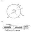
- Japanese Unexamined Patent Application Publication No. 2006-147135 discloses an optical information recording medium 110 which includes at least a dye recording layer 113 containing an organic dye and a light-transmissive layer 116 composed of a resin disposed on a substrate 111 (refer to Figs. 3 and 4 ).
- an intermediate layer 114 is provided between the dye recording layer 113 and the light-transmissive layer 116 (or an adhesive layer 115), the intermediate layer 114 preventing mixing of the dye recording layer 113 and the light-transmissive layer 116 (or adhesive layer 115).
- the intermediate layer 114 is composed of a Ta-containing compound, a Nb-containing compound, or a compound oxide containing Ta and/or Nb.
- the intermediate layer 114 has a thickness of 1 to 80 nm.
- the optical information recording medium 110 described above as the related art includes an intermediate layer 114 composed of an inorganic substance, such as a Ta-containing compound or a Nb-containing compound, disposed between the dye recording layer 113 and the light-transmissive layer 116. Since adhesion between the intermediate layer 114 and the light-transmissive layer 116 (or adhesive layer 115) is not good, delamination easily occurs at the interface between the intermediate layer 114 and the light-transmissive layer 116 (or adhesive layer 115).
- an intermediate layer 114 composed of an inorganic substance, such as a Ta-containing compound or a Nb-containing compound
- an optical information recording medium includes a disk-like substrate having a hole in a central portion thereof, and a light-reflective layer, a dye recording layer containing an organic dye, an intermediate layer composed of an inorganic substance, and a light-transmissive layer composed of a resin disposed in that order on one principal surface of the substrate, in which information is recorded/reproduced by irradiation of laser light from the light-transmissive layer side.
- the light-transmissive layer covers a surface of the intermediate layer from an inner peripheral edge of the intermediate layer to an outer peripheral edge of the intermediate layer, and a vicinity of an outer peripheral edge of the light-transmissive layer is in contact with the substrate in an annular region extending around an outer peripheral side of the substrate. According to the aspect of the present invention, adhesion between the substrate and the light-transmissive layer improves, and consequently, delamination can be prevented from occurring at the interface between the intermediate layer and the light-transmissive layer.
- the optical information recording medium may further include a hard coat layer disposed on the light-transmissive layer.
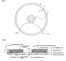
- Fig. 1 is a plan view showing an overall structure of an optical information recording medium according to a first embodiment of the present invention
- Fig. 2 is a longitudinal cross-sectional view showing an internal structure of the optical information recording medium according to the first embodiment
- Fig. 3 is a plan view showing an optical information recording medium according to a related art.
- Fig. 4 is a cross-sectional view showing the optical information recording medium according to the
- FIG. 1 is a plan view showing an overall structure of an optical information recording medium 10 according to the first embodiment.
- Fig. 2 is a longitudinal cross-sectional view showing an internal structure of the optical information recording medium 10 according to the first embodiment.
- the optical information recording medium 10 has a hole in a central portion thereof and has a disk-like outer shape with an outer diameter of about 120 mm, an inner diameter of about 15 mm, and a thickness of about 1.2 mm.
- a substrate 11 has a disk-like outer shape having a hole in a central portion thereof.
- the substrate 11 has a thickness of about 1.1 mm and is composed of a resin. Furthermore, one principal surface 11a of the substrate 11 is provided with a spiral groove (not shown).
- a light-reflective layer 12 composed of an Ag alloy that reflects laser light, which will be described below, is disposed on the principal surface 11a of the substrate 11.
- a groove (not shown) is spirally formed in a surface of the light-reflective layer 12, opposite to the surface in contact with the principal surface 11a provided with the groove, at the same track pitch as that of the groove of the substrate 11 so as to correspond to the groove of the substrate 11.
- the light-reflective layer 12 has a land (not shown) between adjacent segments of the spiral groove.
- a dye recording layer 13 containing a light-absorbing material composed of an organic dye represented by general formula 1 below is disposed on the light-reflective layer 12, the light-absorbing material absorbing laser light with a wavelength of 400 to 420 nm (e.g., 405 nm).
- ring A represents a heterocyclic ring formed together with the carbon atom and the nitrogen atom bonded thereto;
- ring B represents an optionally substituted benzene ring;
- ring C represents a heterocyclic ring containing the nitrogen atom bonded thereto and may form a bond together with the ring B;
- X - represents a group which can have active hydrogen;
- M 2+ represents a divalent metal cation, the dye being a metal complex in which one molecule of M 2+ is bonded to two azo dye molecules represented by anions.
- An intermediate layer 14 made of an inorganic substance composed of a Nb 2 O 5 -Al 2 O 3 -based compound oxide containing 60 mole percent of Nb 2 O 5 is formed on the dye recording layer 13 using a target composed of a Nb 2 O 5 -Al 2 O 3 -based compound oxide containing 60 mole percent of Nb 2 O 5 .
- a light-transmissive layer 16 composed of a transparent resin material is disposed on the intermediate layer 14.
- the light-transmissive layer 16 has a thickness of about 0.1 mm.
- the optical information recording medium 10 according to this embodiment further includes a hard coat layer 17 composed of an ultraviolet curable resin provided on the light-transmissive layer 16 in order to prevent the surface of the light-transmissive layer 16 from being damaged.
- the light-transmissive layer 16 covers the surface of the intermediate layer 14 from the inner peripheral edge to the outer peripheral edge of the intermediate layer 14, and a vicinity of an outer peripheral edge of the light-transmissive layer 16 is in contact with the substrate 11 in an annular region extending around an outer peripheral side 11d of the substrate 11. Consequently, adhesion between the substrate 11 and the light-transmissive layer 16 improves, and thereby, delamination can be prevented from occurring at the interface between the intermediate layer 14 and the light-transmissive layer 16.
- the organic dye in the dye recording layer 13 absorbs the laser light and generates heat to form pits (not shown) which can be optically read, and thus user information can be satisfactory recorded.
- any of various materials for the substrates of the known optical information recording media can be selected for use.
- Specific examples thereof include polycarbonate; acrylic resins, such as and polymethyl methacrylate; vinyl chloride-based resins, such as polyvinyl chloride and vinyl chloride copolymers; epoxy resins: amorphous polyolefins; polyester resins; metals, such as aluminum; and glass.
- polycarbonate acrylic resins, such as and polymethyl methacrylate
- vinyl chloride-based resins such as polyvinyl chloride and vinyl chloride copolymers
- epoxy resins amorphous polyolefins
- polyester resins such as polyvinyl chloride and vinyl chloride copolymers
- metals such as aluminum
- glass glass
- thermoplastic resin is preferable, and polycarbonate is particularly preferable.
- the substrate 11 is formed by injection molding or the like into a predetermined shape (annular shape in the case of an optical disk).
- the thickness of the substrate 11 is preferably in a range of 0.9 to 1.1 mm.
- a die plate which is referred to as a stamper and on which a spiral protrusion having a reverse pattern of the groove on one surface of the substrate 11 is formed by micromachining, is placed in a mold used for injection molding of the substrate 11 so that the spiral groove is formed simultaneously during the injection molding of the substrate 11.
- the groove is generally formed with a pitch of 0.35 or 0.32 ⁇ m.
- the substrate 11 is not limited to that described above.
- a method may be used in which an ultraviolet curable resin is applied by coating onto a base, and the coating film is cured, separated from the base, and used as the substrate 11.
- the light-reflective layer 12 reflects laser light for recording and/or reproducing data, and in the present invention, in order to increase the reflectance with respect to laser light and provide a function of improving recording and reproducing characteristics, preferably, the light-reflective layer 12 is disposed between the substrate 11 and the dye recording layer 13.
- the light-reflective layer 12 is preferably composed of a metal thin film having a high reflectance. Examples thereof include metal films, such as Au, Al, Ag, Cu, and Pd; alloy films of these metals, such as Ag alloy films, Al alloy films, and alloy films in which trace components are added to these metals.
- the light-reflective layer 12 is formed, for example, by vapor deposition, ion plating, sputtering, or the like, on the one principal surface 11a provided with the groove. In view of mass productivity and cost, sputtering is particularly preferable.
- a spiral groove is preferably formed in a surface of the light-reflective layer 12, opposite to the surface in contact with the principal surface 11a of the substrate 11, at the same track pitch as that of the groove of the substrate 11 so as to correspond to the groove of the substrate 11.
- the groove is formed by forming the light-reflective layer 13 by sputtering or the like at a uniform thickness on the one principal surface 11a of the substrate 11 provided with the spiral groove.
- the dye recording layer 13 preferably contains a light-absorbing material composed of an organic dye which absorbs laser light.
- the dye recording layer 13 is a dye-type optical recording layer in which pits are formed by irradiation of laser light, and thus data is recorded.
- the organic dye a phthalocyanine dye, a cyanine dye, an azo-based dye, or the like is preferable, and the azo-based dye represented by general formula 1 below is more preferable.
- ring A represents a heterocyclic ring formed together with the carbon atom and the nitrogen atom bonded thereto;
- ring B represents an optionally substituted benzene ring;
- ring C represents a heterocyclic ring containing the nitrogen atom bonded thereto and may form a bond together with the ring B;
- X - represents a group which can have active hydrogen;
- M 2+ represents a divalent metal cation, the dye being a metal complex in which one molecule of M 2+ is bonded to two azo dye molecules represented by anions.
- the dye recording layer 13 is preferably formed by a method in which a coating solution is prepared by dissolving the dye represented by general formula 1, a binder, etc., in a solvent, such as tetrafluoropropanol (TFP), the coating solution is applied by spin-coating, screen-printing, or the like on the substrate 11 through the light-reflective layer 12 to form a coating film, and then the coating film is dried, for example, at 80°C for 30 minutes.
- a coating solution is prepared by dissolving the dye represented by general formula 1, a binder, etc., in a solvent, such as tetrafluoropropanol (TFP)
- the coating solution is applied by spin-coating, screen-printing, or the like on the substrate 11 through the light-reflective layer 12 to form a coating film, and then the coating film is dried, for example, at 80°C for 30 minutes.
- the intermediate layer 14 is preferably formed between the dye recording layer 13 and the light-transmissive layer 16, which will be described below, in order to prevent mixing of the dye recording layer 13 and the light-transmissive layer 16.
- the intermediate layer 14 is preferably composed of a Nb 2 O 5 -Al 2 O 3 -based compound oxide.
- the intermediate layer 14 is preferably light-transmissive, and is preferably formed, for example, by vapor deposition, ion plating, sputtering, or the like, on the surface provided with the dye recording layer 13. In view of mass productivity and cost, sputtering using an RF sputtering system is particularly preferable.
- an AC (radio frequency) voltage is applied between a conductive vacuum chamber and a target, electrons on the target side have nowhere to go, thus increasing the density, as a result, the target side is negatively biased, ions are attracted to the target, the ions collided with the target sputter the particles of the target, the sputtered particles of the compound oxide collide with and adhere to the dye recording layer 13 of the substrate 11, and thus the intermediate layer (inorganic substance layer) 14 is formed.
- the pressure in the vacuum chamber is preferably set at 1 ⁇ 10 -2 to 1 ⁇ 10 -5 torr, and the sputtering rate is preferably set at 0.1 to 10 nm/sec. Furthermore, the sputtering power is preferably 0.2 to 2.5 kW.
- the light-transmissive layer 16 is preferably composed of a light-transmissive resin, and is preferably formed, by spin-coating or the like, using an ultraviolet resin.
- the thickness of the light-transmissive layer 16 is preferably 0.1 mm so that data can be recorded in and/or read from the dye recording layer 13 by irradiation of laser light with a wavelength of, usually, about 400 to 420 nm (e.g., 405 nm).
- the light transmittance of the light-transmissive layer 16 is preferably 70% or more, and more preferably 80% or more, when measured by a spectrophotometer using light with a wavelength of about 400 to 420 nm (e.g., 405 nm) at a thickness after curing of 0.1 mm.
- the light-transmissive layer 16 covers the surface of the intermediate layer 14 from the inner peripheral edge to the outer peripheral edge of the intermediate layer 14, and a vicinity of an outer peripheral edge of the light-transmissive layer 16 is in contact with the substrate 11 in an annular region extending around an outer peripheral side 11d of the substrate 11.
- the light-transmissive layer 16 is formed on the outer peripheral side 11d of the substrate 11, preferably, by a method in which, before or after the application of the light-transmissive resin by spin-coating or the like described above, the light-transmissive resin is separately applied to the outer peripheral side 11d of the substrate 11.
- the resin is applied to the outer peripheral side 11d of the substrate 11, preferably, by a method in which, for example, a coating means (not shown), such as a transfer roller or a spray nozzle, is arranged so as to face, in contact with or away from, the outer peripheral side 11d of the substrate 11, and using the coating means, the light-transmissive resin is applied to the annular region extending around the outer peripheral side 11d of the substrate 11.
- a coating means such as a transfer roller or a spray nozzle
- the uncured resin irregularly protruding over the outer peripheral side 11d of the substrate 11 in the application process by spin-coating may be spread over the outer peripheral side 11d of the substrate 11 using a roller, a squeegee, or the like arranged in the same manner as above.
- the thickness of the transparent resin formed by coating on the outer peripheral side 11d of the substrate 11 is preferably 100 to 300 ⁇ m, and is preferably equal to or larger than the thickness of the resin applied onto the intermediate layer 14.
- the light-transmissive layer 16 covers the entire surface of the outer peripheral side 11d of the substrate 11 so that the edge of the outer periphery of the light-transmissive layer 16 reaches the lower end of the outer peripheral side 11d of the substrate 11.
- the present invention is not limited thereto as long as the edge of the outer periphery of the light-transmissive layer 16 is in contact with the substrate 11 in the annular region extending around the outer peripheral side 11d of the substrate 11.
- optical information recording medium 10 Examples of an optical information recording medium 10 according to an embodiment of the present invention will be described below.
- a resist film was formed by applying a photoresist (photosensitizing agent) onto a glass board at a predetermined thickness, exposure was performed using laser light of a cutting apparatus so as to achieve a predetermined exposure width, and then a developer was added dropwise onto the resulting glass board to carry out development treatment. Thereby, an irregular resist pattern corresponding to the groove of a substrate of a disk-shaped optical information recording medium was formed. Then, nickel was precipitated by plating treatment on the glass board, and the resulting nickel film was separated from the glass board and trimmed so as to have a disk-like outer shape. Thereby, a stamper was obtained. The stamper was set in a cavity of an injection molding apparatus, and a polycarbonate resin was injected into the cavity. Thereby, a substrate 11 having a spiral groove on one principal surface 11a thereof was obtained.
- a photoresist photosensitizing agent
- An Ag alloy was sputtered to the principal surface 11a of the substrate 11 provided with the spiral groove, at a uniform thickness, using a sputtering system. Thereby, a light-reflective layer 12 with a thickness of 100 nm having a spiral groove corresponding to the groove of the substrate 11 on a surface opposite to the surface in contact with the principal surface 11a of the substrate 11 was formed.
- a dye solution containing an azo-based organic dye represented by general formula 1 was applied by spin-coating onto the light-reflective layer 12 on the substrate 11 at a thickness of 60 nm, followed by drying, to obtain a dye recording layer 13.
- an intermediate layer 14 made of an inorganic substance composed of a Nb 2 O 5 -Al 2 O 3 -based compound oxide containing about 60 mole percent of Nb 2 O 5 with a thickness of 25 nm was formed on the dye recording layer 13 by sputtering under the condition of a sputtering power of 2.0 kW in a sputtering system, using a target composed of a Nb 2 O 5 -Al 2 O 3 -based compound oxide containing 60 mole percent of Nb 2 O 5 .
- the compositions of the target and the intermediate layer 14 were confirmed by an ICP analyzer.
- an ultraviolet curable resin was applied by spin-coating onto the intermediate layer 14 so as to cover the surface of the intermediate layer 14 from the inner peripheral edge to the outer peripheral edge of the intermediate layer 14, and cured by UV irradiation.
- a transfer roller was arranged so as to face the outer peripheral side 11d of the substrate 11, and the same ultraviolet curable resin was applied by a roller transfer method so as to be in contact with the substrate 11 in an annular region extending around the outer peripheral side 11d of the substrate 11, and cured by UV irradiation.
- a light-transmissive layer 16 having a thickness of 0.1 mm on the intermediate layer 14 and a thickness of 200 ⁇ m on the outer peripheral side 11d of the substrate 11 was formed.
- an ultraviolet curable resin composed of an acrylic resin was applied by spin-coating onto the light-transmissive layer 16 to form a hard coat layer 17 with a thickness of 2 to 3 ⁇ m.
- a sample of an optical information recording medium was prepared.
- the appearance of the sample of the optical information recording medium 10 was visually observed from the light-transmissive layer 16 side. As a result, no delamination from the outer peripheral side 11d was found at the interface between the intermediate layer 14 and the light-transmissive layer 16.
- the sample of the optical information recording medium 10 was dropped from a height of 80 cm onto a corner portion of a resin block. With respect to the sample, the occurrence of delamination from the outer peripheral side 11d at the interface between the intermediate layer 14 and the light-transmissive layer 16 was again examined. As a result, no delamination from the outer peripheral side 11d was observed.
- Comparative Example a sample of an optical information recording medium was prepared as in Example except that a transparent resin sheet with a thickness of 0.1 mm was bonded onto the intermediate layer using an ultraviolet curable adhesive layer to form a light-transmissive layer. Then, as in Example, the occurrence of delamination at the interface between the intermediate layer and the light-transmissive layer and the occurrence of delamination from the outer peripheral side after the same drop test as that described above were observed. As a result, in the sample after the drop test, delamination from the outer peripheral side was observed.
- the light-reflective layer 12 and the dye recording layer 13 are disposed in that order on one principal surface 11a of the substrate 11, and the intermediate layer 14 is disposed on the dye recording layer 13.
- the present invention is not limited thereto.
- An intermediate layer 14 may be formed directly or through another layer on one principal surface 11a of the substrate 11.
- the hard coat layer 17 is further disposed on the light-transmissive layer 16.
- the present invention is not limited thereto.
- the hard coat layer 17 may be omitted.
Landscapes
- Optical Record Carriers And Manufacture Thereof (AREA)
Abstract
Description
- The present invention relates to an optical information recording medium, and in particular relates to an optical information recording medium, such as a Blu-ray disc, which includes an optical recording layer containing an organic dye and which has an increased recording density.
- As information recording media, optical information recording media, such as optical disks, are widely used. Examples of such optical information recording media include a medium, such as CD-R, in which a recording layer and a reflection layer are disposed in that order on a light-transmissive resin substrate with a thickness of 1.2 mm and a diameter of 120 mm or 80 mm. In recent years, a higher information recording density has been required. Under these circumstances, a method has been conceived in which the laser wavelength is decreased and an object lens having a high numerical aperture (NA) is used, and thus, optical information recording media, such as DVD+R and DVD-R, have been realized. DVD+R or DVD-R has a structure in which, in order to increase the permissible value of the angle of tilt of the disk due to a decrease in wavelength and an increase in NA, two light-transmissive resin substrates with a thickness of 0.6 mm are bonded to each other with a reflection layer and a recording layer provided therebetween.
- Furthermore, in recent years, in order to record high-definition image data, a much higher information recording density has been required. Under these circumstances, an optical information recording medium has been proposed which, as in a Blu-ray disc (BD-R), has a structure in which a reflection layer and a recording layer are disposed on a surface of a resin substrate with a thickness of 1.1 mm, and a light-transmissive layer with a thickness of 0.1 mm is disposed so as to cover the surface provided with the reflection layer and the recording layer. Specifically, the optical information recording medium includes a light-reflective layer, a phase-change recording layer, and a light-transmissive layer with a thickness of about 0.1 mm disposed on a disk-shaped substrate having an outer diameter of 120 mm, an inner diameter of 15 mm, and a thickness of about 1.1 mm, and by performing irradiation of laser light with a wavelength of about 405 nm from an optical head with a numerical aperture of about 0.85, user information can be recorded in the recording layer.
- Use of a recording layer containing a dye, instead of the phase-change recording layer, is also under study. Japanese Unexamined Patent Application Publication No.
2006-147135 information recording medium 110 which includes at least adye recording layer 113 containing an organic dye and a light-transmissive layer 116 composed of a resin disposed on a substrate 111 (refer toFigs. 3 and 4 ). In the opticalinformation recording medium 110, anintermediate layer 114 is provided between thedye recording layer 113 and the light-transmissive layer 116 (or an adhesive layer 115), theintermediate layer 114 preventing mixing of thedye recording layer 113 and the light-transmissive layer 116 (or adhesive layer 115). Theintermediate layer 114 is composed of a Ta-containing compound, a Nb-containing compound, or a compound oxide containing Ta and/or Nb. Theintermediate layer 114 has a thickness of 1 to 80 nm. - The optical
information recording medium 110 described above as the related art includes anintermediate layer 114 composed of an inorganic substance, such as a Ta-containing compound or a Nb-containing compound, disposed between thedye recording layer 113 and the light-transmissive layer 116. Since adhesion between theintermediate layer 114 and the light-transmissive layer 116 (or adhesive layer 115) is not good, delamination easily occurs at the interface between theintermediate layer 114 and the light-transmissive layer 116 (or adhesive layer 115). In particular, when a user drops by mistake the opticalinformation recording medium 110 to the floor or the like, delamination easily occurs from an outerperipheral side 111d of the opticalinformation recording medium 110 at the interface between theintermediate layer 114 and the light-transmissive layer 116 (or adhesive layer 115). The occurrence of delamination at the interface between theintermediate layer 114 and the light-transmissive layer 116 (or adhesive layer 115) results in degradation in quality in terms of appearance as well as degradation in environmental resistance (moisture resistance), etc., which is a problem. - It is an object of the present invention to provide an optical information recording medium in which delamination does not occur at the interface between an intermediate layer and a light-transmissive layer, unlike in the related art.
- In order to achieve the object described above, according to an aspect of the present invention, an optical information recording medium includes a disk-like substrate having a hole in a central portion thereof, and a light-reflective layer, a dye recording layer containing an organic dye, an intermediate layer composed of an inorganic substance, and a light-transmissive layer composed of a resin disposed in that order on one principal surface of the substrate, in which information is recorded/reproduced by irradiation of laser light from the light-transmissive layer side. In the optical information recording medium, the light-transmissive layer covers a surface of the intermediate layer from an inner peripheral edge of the intermediate layer to an outer peripheral edge of the intermediate layer, and a vicinity of an outer peripheral edge of the light-transmissive layer is in contact with the substrate in an annular region extending around an outer peripheral side of the substrate. According to the aspect of the present invention, adhesion between the substrate and the light-transmissive layer improves, and consequently, delamination can be prevented from occurring at the interface between the intermediate layer and the light-transmissive layer.
- According to an embodiment of the present invention, the optical information recording medium may further include a hard coat layer disposed on the light-transmissive layer.
- The above object and other objects, features, and operational advantages of the present invention will become apparent from the following description of preferred embodiments with reference to the attached drawings.
-
Fig. 1 is a plan view showing an overall structure of an optical information recording medium according to a first embodiment of the present invention; -
Fig. 2 is a longitudinal cross-sectional view showing an internal structure of the optical information recording medium according to the first embodiment; -
Fig. 3 is a plan view showing an optical information recording medium according to a related art; and -
Fig. 4 is a cross-sectional view showing the optical information recording medium according to the - An optical information recording medium according to a first embodiment of the present invention will be described below with reference to
Figs. 1 and 2. Fig. 1 is a plan view showing an overall structure of an opticalinformation recording medium 10 according to the first embodiment.Fig. 2 is a longitudinal cross-sectional view showing an internal structure of the opticalinformation recording medium 10 according to the first embodiment. - As shown in
Figs. 1 and 2 , the opticalinformation recording medium 10 according to this embodiment has a hole in a central portion thereof and has a disk-like outer shape with an outer diameter of about 120 mm, an inner diameter of about 15 mm, and a thickness of about 1.2 mm. - As is obvious from the drawings, a
substrate 11 has a disk-like outer shape having a hole in a central portion thereof. Thesubstrate 11 has a thickness of about 1.1 mm and is composed of a resin. Furthermore, oneprincipal surface 11a of thesubstrate 11 is provided with a spiral groove (not shown). - A light-reflective layer 12 composed of an Ag alloy that reflects laser light, which will be described below, is disposed on the
principal surface 11a of thesubstrate 11. A groove (not shown) is spirally formed in a surface of the light-reflective layer 12, opposite to the surface in contact with theprincipal surface 11a provided with the groove, at the same track pitch as that of the groove of thesubstrate 11 so as to correspond to the groove of thesubstrate 11. The light-reflective layer 12 has a land (not shown) between adjacent segments of the spiral groove. - A dye recording layer 13 containing a light-absorbing material composed of an organic dye represented by general formula 1 below is disposed on the light-reflective layer 12, the light-absorbing material absorbing laser light with a wavelength of 400 to 420 nm (e.g., 405 nm).


- In general formula 1, ring A represents a heterocyclic ring formed together with the carbon atom and the nitrogen atom bonded thereto; ring B represents an optionally substituted benzene ring; ring C represents a heterocyclic ring containing the nitrogen atom bonded thereto and may form a bond together with the ring B; X- represents a group which can have active hydrogen; and M2+ represents a divalent metal cation, the dye being a metal complex in which one molecule of M2+ is bonded to two azo dye molecules represented by anions.
- An intermediate layer 14 made of an inorganic substance composed of a Nb2O5-Al2O3-based compound oxide containing 60 mole percent of Nb2O5 is formed on the dye recording layer 13 using a target composed of a Nb2O5-Al2O3-based compound oxide containing 60 mole percent of Nb2O5.
- A light-
transmissive layer 16 composed of a transparent resin material is disposed on the intermediate layer 14. The light-transmissive layer 16 has a thickness of about 0.1 mm. The opticalinformation recording medium 10 according to this embodiment further includes ahard coat layer 17 composed of an ultraviolet curable resin provided on the light-transmissive layer 16 in order to prevent the surface of the light-transmissive layer 16 from being damaged. - In the optical
information recording medium 10 according to this embodiment, the light-transmissive layer 16 covers the surface of the intermediate layer 14 from the inner peripheral edge to the outer peripheral edge of the intermediate layer 14, and a vicinity of an outer peripheral edge of the light-transmissive layer 16 is in contact with thesubstrate 11 in an annular region extending around an outerperipheral side 11d of thesubstrate 11. Consequently, adhesion between thesubstrate 11 and the light-transmissive layer 16 improves, and thereby, delamination can be prevented from occurring at the interface between the intermediate layer 14 and the light-transmissive layer 16. - When laser light with a wavelength of 400 to 420 nm (e.g., 405 nm) is applied to the optical
information recording medium 10 from the light-transmissive layer 16 side, the organic dye in the dye recording layer 13 absorbs the laser light and generates heat to form pits (not shown) which can be optically read, and thus user information can be satisfactory recorded. - A preferred embodiment of the
substrate 11 will be described below. As thesubstrate 11, any of various materials for the substrates of the known optical information recording media can be selected for use.
Specific examples thereof include polycarbonate; acrylic resins, such as and polymethyl methacrylate; vinyl chloride-based resins, such as polyvinyl chloride and vinyl chloride copolymers; epoxy resins: amorphous polyolefins; polyester resins; metals, such as aluminum; and glass. As required, these may be used in combination. Among the materials described above, in view of moldability, moisture resistance, dimensional stability, low cost, etc., a thermoplastic resin is preferable, and polycarbonate is particularly preferable. - When any of these resins is used, preferably, the
substrate 11 is formed by injection molding or the like into a predetermined shape (annular shape in the case of an optical disk). The thickness of thesubstrate 11 is preferably in a range of 0.9 to 1.1 mm. In this step, preferably, a die plate, which is referred to as a stamper and on which a spiral protrusion having a reverse pattern of the groove on one surface of thesubstrate 11 is formed by micromachining, is placed in a mold used for injection molding of thesubstrate 11 so that the spiral groove is formed simultaneously during the injection molding of thesubstrate 11. The groove is generally formed with a pitch of 0.35 or 0.32 µm. Furthermore, thesubstrate 11 is not limited to that described above. For example, a method may be used in which an ultraviolet curable resin is applied by coating onto a base, and the coating film is cured, separated from the base, and used as thesubstrate 11. - A preferred embodiment of the light-reflective layer 12 will be described below. The light-reflective layer 12 reflects laser light for recording and/or reproducing data, and in the present invention, in order to increase the reflectance with respect to laser light and provide a function of improving recording and reproducing characteristics, preferably, the light-reflective layer 12 is disposed between the
substrate 11 and the dye recording layer 13. The light-reflective layer 12 is preferably composed of a metal thin film having a high reflectance. Examples thereof include metal films, such as Au, Al, Ag, Cu, and Pd; alloy films of these metals, such as Ag alloy films, Al alloy films, and alloy films in which trace components are added to these metals. Preferably, the light-reflective layer 12 is formed, for example, by vapor deposition, ion plating, sputtering, or the like, on the oneprincipal surface 11a provided with the groove. In view of mass productivity and cost, sputtering is particularly preferable. A spiral groove is preferably formed in a surface of the light-reflective layer 12, opposite to the surface in contact with theprincipal surface 11a of thesubstrate 11, at the same track pitch as that of the groove of thesubstrate 11 so as to correspond to the groove of thesubstrate 11. Preferably, the groove is formed by forming the light-reflective layer 13 by sputtering or the like at a uniform thickness on the oneprincipal surface 11a of thesubstrate 11 provided with the spiral groove. - A preferred embodiment of the dye recording layer 13 will be described below. The dye recording layer 13 preferably contains a light-absorbing material composed of an organic dye which absorbs laser light. In particular, the dye recording layer 13 is a dye-type optical recording layer in which pits are formed by irradiation of laser light, and thus data is recorded. As the organic dye, a phthalocyanine dye, a cyanine dye, an azo-based dye, or the like is preferable, and the azo-based dye represented by general formula 1 below is more preferable.


- In general formula 1, ring A represents a heterocyclic ring formed together with the carbon atom and the nitrogen atom bonded thereto; ring B represents an optionally substituted benzene ring; ring C represents a heterocyclic ring containing the nitrogen atom bonded thereto and may form a bond together with the ring B; X- represents a group which can have active hydrogen; and M2+ represents a divalent metal cation, the dye being a metal complex in which one molecule of M2+ is bonded to two azo dye molecules represented by anions.
- The dye recording layer 13 is preferably formed by a method in which a coating solution is prepared by dissolving the dye represented by general formula 1, a binder, etc., in a solvent, such as tetrafluoropropanol (TFP), the coating solution is applied by spin-coating, screen-printing, or the like on the
substrate 11 through the light-reflective layer 12 to form a coating film, and then the coating film is dried, for example, at 80°C for 30 minutes. - A preferred embodiment of the intermediate layer 14 will be described below. The intermediate layer 14 is preferably formed between the dye recording layer 13 and the light-
transmissive layer 16, which will be described below, in order to prevent mixing of the dye recording layer 13 and the light-transmissive layer 16. The intermediate layer 14 is preferably composed of a Nb2O5-Al2O3-based compound oxide. However, the present invention is not limited thereto, and various changes are possible. The intermediate layer 14 is preferably light-transmissive, and is preferably formed, for example, by vapor deposition, ion plating, sputtering, or the like, on the surface provided with the dye recording layer 13. In view of mass productivity and cost, sputtering using an RF sputtering system is particularly preferable.
In the RF sputtering system, an AC (radio frequency) voltage is applied between a conductive vacuum chamber and a target, electrons on the target side have nowhere to go, thus increasing the density, as a result, the target side is negatively biased, ions are attracted to the target, the ions collided with the target sputter the particles of the target, the sputtered particles of the compound oxide collide with and adhere to the dye recording layer 13 of thesubstrate 11, and thus the intermediate layer (inorganic substance layer) 14 is formed. When the intermediate layer 14 is formed by sputtering using the RF sputtering system, the pressure in the vacuum chamber is preferably set at 1 × 10⁻² to 1 × 10⁻⁵ torr, and the sputtering rate is preferably set at 0.1 to 10 nm/sec. Furthermore, the sputtering power is preferably 0.2 to 2.5 kW. - A preferred embodiment of the light-
transmissive layer 16 will be described below. The light-transmissive layer 16 is preferably composed of a light-transmissive resin, and is preferably formed, by spin-coating or the like, using an ultraviolet resin. The thickness of the light-transmissive layer 16 is preferably 0.1 mm so that data can be recorded in and/or read from the dye recording layer 13 by irradiation of laser light with a wavelength of, usually, about 400 to 420 nm (e.g., 405 nm). The light transmittance of the light-transmissive layer 16 is preferably 70% or more, and more preferably 80% or more, when measured by a spectrophotometer using light with a wavelength of about 400 to 420 nm (e.g., 405 nm) at a thickness after curing of 0.1 mm. - Furthermore, preferably, the light-
transmissive layer 16 covers the surface of the intermediate layer 14 from the inner peripheral edge to the outer peripheral edge of the intermediate layer 14, and a vicinity of an outer peripheral edge of the light-transmissive layer 16 is in contact with thesubstrate 11 in an annular region extending around an outerperipheral side 11d of thesubstrate 11. - The light-
transmissive layer 16 is formed on the outerperipheral side 11d of thesubstrate 11, preferably, by a method in which, before or after the application of the light-transmissive resin by spin-coating or the like described above, the light-transmissive resin is separately applied to the outerperipheral side 11d of thesubstrate 11. - The resin is applied to the outer
peripheral side 11d of thesubstrate 11, preferably, by a method in which, for example, a coating means (not shown), such as a transfer roller or a spray nozzle, is arranged so as to face, in contact with or away from, the outerperipheral side 11d of thesubstrate 11, and using the coating means, the light-transmissive resin is applied to the annular region extending around the outerperipheral side 11d of thesubstrate 11. By this method, the resin can be applied with a uniform thickness to the outerperipheral side 11d of thesubstrate 11. The present invention is not limited thereto. For example, the uncured resin irregularly protruding over the outerperipheral side 11d of thesubstrate 11 in the application process by spin-coating may be spread over the outerperipheral side 11d of thesubstrate 11 using a roller, a squeegee, or the like arranged in the same manner as above. - The thickness of the transparent resin formed by coating on the outer
peripheral side 11d of thesubstrate 11 is preferably 100 to 300 µm, and is preferably equal to or larger than the thickness of the resin applied onto the intermediate layer 14. Furthermore, the light-transmissive layer 16 covers the entire surface of the outerperipheral side 11d of thesubstrate 11 so that the edge of the outer periphery of the light-transmissive layer 16 reaches the lower end of the outerperipheral side 11d of thesubstrate 11. However, the present invention is not limited thereto as long as the edge of the outer periphery of the light-transmissive layer 16 is in contact with thesubstrate 11 in the annular region extending around the outerperipheral side 11d of thesubstrate 11. - Examples of an optical
information recording medium 10 according to an embodiment of the present invention will be described below. - A resist film was formed by applying a photoresist (photosensitizing agent) onto a glass board at a predetermined thickness, exposure was performed using laser light of a cutting apparatus so as to achieve a predetermined exposure width, and then a developer was added dropwise onto the resulting glass board to carry out development treatment. Thereby, an irregular resist pattern corresponding to the groove of a substrate of a disk-shaped optical information recording medium was formed. Then, nickel was precipitated by plating treatment on the glass board, and the resulting nickel film was separated from the glass board and trimmed so as to have a disk-like outer shape. Thereby, a stamper was obtained. The stamper was set in a cavity of an injection molding apparatus, and a polycarbonate resin was injected into the cavity. Thereby, a
substrate 11 having a spiral groove on oneprincipal surface 11a thereof was obtained. - An Ag alloy was sputtered to the
principal surface 11a of thesubstrate 11 provided with the spiral groove, at a uniform thickness, using a sputtering system. Thereby, a light-reflective layer 12 with a thickness of 100 nm having a spiral groove corresponding to the groove of thesubstrate 11 on a surface opposite to the surface in contact with theprincipal surface 11a of thesubstrate 11 was formed. - Furthermore, a dye solution containing an azo-based organic dye represented by general formula 1 was applied by spin-coating onto the light-reflective layer 12 on the
substrate 11 at a thickness of 60 nm, followed by drying, to obtain a dye recording layer 13. - Then, an intermediate layer 14 made of an inorganic substance composed of a Nb2O5-Al2O3-based compound oxide containing about 60 mole percent of Nb2O5 with a thickness of 25 nm was formed on the dye recording layer 13 by sputtering under the condition of a sputtering power of 2.0 kW in a sputtering system, using a target composed of a Nb2O5-Al2O3-based compound oxide containing 60 mole percent of Nb2O5. The compositions of the target and the intermediate layer 14 were confirmed by an ICP analyzer.
- Next, an ultraviolet curable resin was applied by spin-coating onto the intermediate layer 14 so as to cover the surface of the intermediate layer 14 from the inner peripheral edge to the outer peripheral edge of the intermediate layer 14, and cured by UV irradiation. Then, a transfer roller was arranged so as to face the outer
peripheral side 11d of thesubstrate 11, and the same ultraviolet curable resin was applied by a roller transfer method so as to be in contact with thesubstrate 11 in an annular region extending around the outerperipheral side 11d of thesubstrate 11, and cured by UV irradiation. Thereby, a light-transmissive layer 16 having a thickness of 0.1 mm on the intermediate layer 14 and a thickness of 200 µm on the outerperipheral side 11d of thesubstrate 11 was formed. Furthermore, an ultraviolet curable resin composed of an acrylic resin was applied by spin-coating onto the light-transmissive layer 16 to form ahard coat layer 17 with a thickness of 2 to 3 µm. Thereby, a sample of an optical information recording medium was prepared. - The appearance of the sample of the optical
information recording medium 10 was visually observed from the light-transmissive layer 16 side. As a result, no delamination from the outerperipheral side 11d was found at the interface between the intermediate layer 14 and the light-transmissive layer 16. Next, the sample of the opticalinformation recording medium 10 was dropped from a height of 80 cm onto a corner portion of a resin block. With respect to the sample, the occurrence of delamination from the outerperipheral side 11d at the interface between the intermediate layer 14 and the light-transmissive layer 16 was again examined. As a result, no delamination from the outerperipheral side 11d was observed. - In Comparative Example, a sample of an optical information recording medium was prepared as in Example except that a transparent resin sheet with a thickness of 0.1 mm was bonded onto the intermediate layer using an ultraviolet curable adhesive layer to form a light-transmissive layer. Then, as in Example, the occurrence of delamination at the interface between the intermediate layer and the light-transmissive layer and the occurrence of delamination from the outer peripheral side after the same drop test as that described above were observed. As a result, in the sample after the drop test, delamination from the outer peripheral side was observed.
- In the optical
information recording medium 10 according to the first embodiment, the light-reflective layer 12 and the dye recording layer 13 are disposed in that order on oneprincipal surface 11a of thesubstrate 11, and the intermediate layer 14 is disposed on the dye recording layer 13. However, the present invention is not limited thereto. An intermediate layer 14 may be formed directly or through another layer on oneprincipal surface 11a of thesubstrate 11. Furthermore, in the opticalinformation recording medium 10 according to the first embodiment, thehard coat layer 17 is further disposed on the light-transmissive layer 16. However, the present invention is not limited thereto. Thehard coat layer 17 may be omitted.
Claims (2)
- An optical information recording medium comprising:a disk-like substrate having a hole in a central portion thereof; anda light-reflective layer, a dye recording layer containing an organic dye, an intermediate layer composed of an inorganic substance, and a light-transmissive layer composed of a resin disposed in that order on one principal surface of the substrate, in which information is recorded/reproduced by irradiation of laser light from the light-transmissive layer side,wherein the light-transmissive layer covers a surface of the intermediate layer from an inner peripheral edge of the intermediate layer to an outer peripheral edge of the intermediate layer, and a vicinity of an outer peripheral edge of the light-transmissive layer is in contact with the substrate in an annular region extending around an outer peripheral side of the substrate.
- The optical information recording medium according to Claim 1, further comprising a hard coat layer disposed on the light-transmissive layer.
Applications Claiming Priority (1)
| Application Number | Priority Date | Filing Date | Title |
|---|---|---|---|
| JP2007247557A JP2009080871A (en) | 2007-09-25 | 2007-09-25 | Optical information recording medium |
Publications (1)
| Publication Number | Publication Date |
|---|---|
| EP2045805A1 true EP2045805A1 (en) | 2009-04-08 |
Family
ID=40104659
Family Applications (1)
| Application Number | Title | Priority Date | Filing Date |
|---|---|---|---|
| EP08253070A Withdrawn EP2045805A1 (en) | 2007-09-25 | 2008-09-18 | Optical information recording medium |
Country Status (5)
| Country | Link |
|---|---|
| US (1) | US7835257B2 (en) |
| EP (1) | EP2045805A1 (en) |
| JP (1) | JP2009080871A (en) |
| CN (1) | CN101404165A (en) |
| TW (1) | TWI386935B (en) |
Families Citing this family (3)
| Publication number | Priority date | Publication date | Assignee | Title |
|---|---|---|---|---|
| JP4695632B2 (en) * | 2007-10-05 | 2011-06-08 | 太陽誘電株式会社 | Optical information recording medium |
| JP2012164372A (en) * | 2011-02-03 | 2012-08-30 | Sony Corp | Manufacturing method of optical information recording medium and optical information recording medium |
| JP2016207234A (en) * | 2013-10-03 | 2016-12-08 | パナソニックIpマネジメント株式会社 | Optical information recording medium |
Citations (3)
| Publication number | Priority date | Publication date | Assignee | Title |
|---|---|---|---|---|
| EP0245833A2 (en) * | 1986-05-14 | 1987-11-19 | Teijin Limited | Magneto-optical recording medium |
| EP0398662A2 (en) * | 1989-05-15 | 1990-11-22 | Sharp Kabushiki Kaisha | Process for manufacturing a magneto-optic disc, and a magneto-optic disc manufactured by such a process |
| JP2006147135A (en) | 2004-10-20 | 2006-06-08 | Fuji Photo Film Co Ltd | Optical recording medium |
Family Cites Families (5)
| Publication number | Priority date | Publication date | Assignee | Title |
|---|---|---|---|---|
| EP0404521A3 (en) * | 1989-06-21 | 1991-05-02 | Hitachi Maxell Ltd. | Optical recording medium and method for manufacturing the same |
| JP3588608B2 (en) * | 2002-05-31 | 2004-11-17 | 株式会社東芝 | Optical disc and optical disc manufacturing method |
| TWI317516B (en) * | 2002-06-07 | 2009-11-21 | Fujifilm Corp | Photo-data recording media |
| JP2005111756A (en) * | 2003-10-06 | 2005-04-28 | Fuji Photo Film Co Ltd | Hard-coated article, curable composition, and information recording carrier |
| TW200621645A (en) | 2004-10-20 | 2006-07-01 | Fuji Photo Film Co Ltd | Optical recording medium |
-
2007
- 2007-09-25 JP JP2007247557A patent/JP2009080871A/en not_active Withdrawn
-
2008
- 2008-09-01 TW TW097133498A patent/TWI386935B/en not_active IP Right Cessation
- 2008-09-18 EP EP08253070A patent/EP2045805A1/en not_active Withdrawn
- 2008-09-23 CN CNA2008101613483A patent/CN101404165A/en active Pending
- 2008-09-24 US US12/237,324 patent/US7835257B2/en not_active Expired - Fee Related
Patent Citations (3)
| Publication number | Priority date | Publication date | Assignee | Title |
|---|---|---|---|---|
| EP0245833A2 (en) * | 1986-05-14 | 1987-11-19 | Teijin Limited | Magneto-optical recording medium |
| EP0398662A2 (en) * | 1989-05-15 | 1990-11-22 | Sharp Kabushiki Kaisha | Process for manufacturing a magneto-optic disc, and a magneto-optic disc manufactured by such a process |
| JP2006147135A (en) | 2004-10-20 | 2006-06-08 | Fuji Photo Film Co Ltd | Optical recording medium |
Also Published As
| Publication number | Publication date |
|---|---|
| CN101404165A (en) | 2009-04-08 |
| TWI386935B (en) | 2013-02-21 |
| US20090116369A1 (en) | 2009-05-07 |
| JP2009080871A (en) | 2009-04-16 |
| TW200923939A (en) | 2009-06-01 |
| US7835257B2 (en) | 2010-11-16 |
Similar Documents
| Publication | Publication Date | Title |
|---|---|---|
| TWI240924B (en) | Optical information recording medium and method of manufacturing optical information recording medium | |
| EP1139340B1 (en) | Optical recording medium having an oriented silver reflecting layer | |
| US7835257B2 (en) | Optical information recording medium | |
| US20080241525A1 (en) | Stamper for optical information recording medium, master for magnetic transfer, and manufacturing methods thereof | |
| JP4755680B2 (en) | Optical information recording medium and manufacturing method thereof | |
| EP1811516A1 (en) | Optical information recording medium and method for manufacturing same | |
| JP4695632B2 (en) | Optical information recording medium | |
| HK1126889A (en) | Optical information recording medium | |
| JP4410141B2 (en) | Optical information recording medium | |
| JP2007294055A (en) | Optical information recording medium and method of manufacturing optical information recording medium | |
| JP3600177B2 (en) | Optical recording medium and manufacturing method thereof | |
| JP3718076B2 (en) | Optical information recording medium | |
| US8119216B2 (en) | Optical information recording medium and manufacturing method thereof | |
| JP4312211B2 (en) | Optical information recording medium and manufacturing method thereof | |
| JP2007152825A (en) | Manufacturing method of optical recording medium | |
| JP2004030785A (en) | Optical recording medium | |
| JPH1125509A (en) | Information recording medium | |
| WO2006093038A1 (en) | Stamper, die and method for manufacturing optical disc substrate | |
| JP2010134978A (en) | Method and device for manufacturing optical recording medium | |
| JP2003263786A (en) | Optical information recording medium | |
| HK1129943B (en) | Optical information recording medium | |
| JP2000268402A (en) | Optical information recording medium | |
| JP2007280574A (en) | Information recording method | |
| JP2008041187A (en) | Optical disc bonding method, optical disc manufacturing apparatus, and optical disc manufacturing method | |
| JP2001056971A (en) | Method of manufacturing optical disk medium and optical disk medium |
Legal Events
| Date | Code | Title | Description |
|---|---|---|---|
| PUAI | Public reference made under article 153(3) epc to a published international application that has entered the european phase |
Free format text: ORIGINAL CODE: 0009012 |
|
| AK | Designated contracting states |
Kind code of ref document: A1 Designated state(s): AT BE BG CH CY CZ DE DK EE ES FI FR GB GR HR HU IE IS IT LI LT LU LV MC MT NL NO PL PT RO SE SI SK TR |
|
| AX | Request for extension of the european patent |
Extension state: AL BA MK RS |
|
| 17P | Request for examination filed |
Effective date: 20090306 |
|
| 17Q | First examination report despatched |
Effective date: 20090515 |
|
| AKX | Designation fees paid |
Designated state(s): AT BE BG CH CY CZ DE DK EE ES FI FR GB GR HR HU IE IS IT LI LT LU LV MC MT NL NO PL PT RO SE SI SK TR |
|
| STAA | Information on the status of an ep patent application or granted ep patent |
Free format text: STATUS: THE APPLICATION IS DEEMED TO BE WITHDRAWN |
|
| 18D | Application deemed to be withdrawn |
Effective date: 20090926 |