EP2040380A2 - EL emitting touch switch - Google Patents
EL emitting touch switch Download PDFInfo
- Publication number
- EP2040380A2 EP2040380A2 EP08005164A EP08005164A EP2040380A2 EP 2040380 A2 EP2040380 A2 EP 2040380A2 EP 08005164 A EP08005164 A EP 08005164A EP 08005164 A EP08005164 A EP 08005164A EP 2040380 A2 EP2040380 A2 EP 2040380A2
- Authority
- EP
- European Patent Office
- Prior art keywords
- electrode
- electrodes
- touch
- touch switch
- emitting
- Prior art date
- Legal status (The legal status is an assumption and is not a legal conclusion. Google has not performed a legal analysis and makes no representation as to the accuracy of the status listed.)
- Granted
Links
Images


Classifications
-
- H—ELECTRICITY
- H01—ELECTRIC ELEMENTS
- H01H—ELECTRIC SWITCHES; RELAYS; SELECTORS; EMERGENCY PROTECTIVE DEVICES
- H01H13/00—Switches having rectilinearly-movable operating part or parts adapted for pushing or pulling in one direction only, e.g. push-button switch
- H01H13/70—Switches having rectilinearly-movable operating part or parts adapted for pushing or pulling in one direction only, e.g. push-button switch having a plurality of operating members associated with different sets of contacts, e.g. keyboard
- H01H13/702—Switches having rectilinearly-movable operating part or parts adapted for pushing or pulling in one direction only, e.g. push-button switch having a plurality of operating members associated with different sets of contacts, e.g. keyboard with contacts carried by or formed from layers in a multilayer structure, e.g. membrane switches
-
- H—ELECTRICITY
- H03—ELECTRONIC CIRCUITRY
- H03K—PULSE TECHNIQUE
- H03K17/00—Electronic switching or gating, i.e. not by contact-making and –breaking
- H03K17/94—Electronic switching or gating, i.e. not by contact-making and –breaking characterised by the way in which the control signals are generated
- H03K17/96—Touch switches
- H03K17/962—Capacitive touch switches
- H03K17/9622—Capacitive touch switches using a plurality of detectors, e.g. keyboard
-
- H—ELECTRICITY
- H01—ELECTRIC ELEMENTS
- H01H—ELECTRIC SWITCHES; RELAYS; SELECTORS; EMERGENCY PROTECTIVE DEVICES
- H01H36/00—Switches actuated by change of magnetic field or of electric field, e.g. by change of relative position of magnet and switch, by shielding
-
- H—ELECTRICITY
- H03—ELECTRONIC CIRCUITRY
- H03K—PULSE TECHNIQUE
- H03K2217/00—Indexing scheme related to electronic switching or gating, i.e. not by contact-making or -breaking covered by H03K17/00
- H03K2217/94—Indexing scheme related to electronic switching or gating, i.e. not by contact-making or -breaking covered by H03K17/00 characterised by the way in which the control signal is generated
- H03K2217/96—Touch switches
- H03K2217/9607—Capacitive touch switches
- H03K2217/960785—Capacitive touch switches with illumination
Definitions
- This invention relates to EL (electroluminescence) emitting touch switches utilizing EL in combination with a touch switch, and more particularly, to an EL emitting touch switch provided with a plurality of touch detection electrodes.
- Touch switches have been conventionally known which are provided with conductive electrodes for detecting the contact or proximity of part of a human body with or to the electrodes.
- the electrode functions as a capacitance sensor, and the on/off operation of the touch switch is detected based on change in the impedance (electrostatic capacitance) of the electrode induced by the contact of a human body with the electrode.
- Patent Document 1 Unexamined Japanese Patent Publication No. H05-135654
- FIG. 3 is a schematic sectional view of an example of the body of the touch switch disclosed in Patent Document 1.
- the body of the touch switch has a transparent, electrically insulating substrate 2, a transparent electrode 5 formed on a surface (upper surface) of the substrate 2, and a transparent insulating film 6 covering the upper surface of the electrode 5 and forming a touch surface.
- an EL layer 1 is formed on the reverse surface (lower surface) of the transparent insulating substrate 2.
- the EL layer 1 is formed by successively laminating, from the substrate side downward, a transparent electrode 1a, a phosphor layer 1b, an insulating layer 1c, and a back electrode 1d.
- an alternating-current (AC) voltage is applied between the two electrodes 1a and 1d, the EL layer 1 emits light.
- the emitted light propagates through the transparent electrode 1a, the transparent insulating substrate 2, the transparent touch detection electrode 5 and the transparent insulating film 6 to the outside of the touch switch, thus enabling the operator to easily locate the transparent insulating film 2 with the aid of the emitted light and touch the switch with his/her finger.
- a touch decision circuit not shown, connected to the transparent touch detection electrode 5 detects a change of the impedance or capacitance and judges that the transparent insulating film 6 is touched by the operator. Based on the judgment, the on-off control of a device connected to the touch decision circuit may be executed.
- This touch switch essentially requires, however, a pair of electrodes 1a and 1d for driving the EL layer 1 to emit light, as well as the transparent touch detection electrode 5. It is therefore difficult to reduce the thickness of the touch switch, and also since the number of electrode layers is large, the cost increases.
- Patent Document 2 discloses an EL emitting touch switch in which the touch detection electrode and the EL driving electrode are unified into one common electrode, thereby making it possible to reduce the thickness of the touch switch.
- FIG. 4 schematically shows the configuration of the EL emitting touch switch disclosed in Patent Document 2.
- the switch body 10 of the touch switch includes an EL layer 1, which is a laminate having a phosphor layer 1b and an insulating layer 1c sandwiched between a transparent electrode (surface electrode) 1a and a back electrode 1d.
- the EL layer 1 is formed on an insulating substrate 3 and covered with a transparent insulating film 6.
- the transparent electrode 1a functions as both the touch detection electrode and the EL driving electrode.
- a touch decision circuit 100 detects change in potential of the transparent electrode 1a, to thereby detect the contact of part of the operator's body with the transparent insulating film 6.
- the EL driver circuit 200 outputs an AC voltage based on the potential of the transparent electrode 1a, to cause the EL layer 1 to emit light.
- the switch body 10 is further provided with a drive control circuit 300, in addition to the touch decision circuit 100 and the EL driver circuit 200.
- the touch decision circuit 100 operates in accordance with a control signal from the drive control circuit 300.
- the touch decision circuit 100 is so configured as to detect the contact of the operator's finger with the transparent insulating film 6 on the basis of change in the difference between the potential VA of the transparent electrode 1a and a ground potential VG.
- the drive control circuit 300 drives the EL driver circuit 200 to apply an AC electric field between the electrodes 1a and 1d, thereby controlling the emission of light from the EL layer 1.
- touch switches such as those described above are applied to a control panel for equipment (specifically, audio equipment or an air conditioner) installed in the passenger compartment of an automobile.
- a control panel for equipment specifically, audio equipment or an air conditioner
- the disclosed touch switch is not suited for use in the control panel of, for example, audio equipment or air conditioner of an automobile.
- the touch detection electrode (transparent electrode 1a) used is one in number, but the disclosed technique fails to provide an effective solution in cases where a plurality of touch detection electrodes exist in the same panel, as in a control panel for an automobile device.
- the back electrode 1d generally has an area covering all light emitting regions so as to be used as a common electrode.
- the EL panel is configured in the manner disclosed in Patent Document 2 such that the EL driver circuit is connected to the transparent electrode 1a and the back electrode 1d so as to operate based on the potential of the transparent electrode 1a serving also as the touch detection electrode, that is, the potential of the back electrode 1d is floating with respect to the ground potential, large electrostatic capacitance exists between the transparent electrode 1a, which constitutes an independent light emitting region, and the back electrode 1d. Consequently, when one of the multiple touch detection electrodes is touched by the operator, the touch is detected with respect to all switches at the same time (see FIG. 5 ).
- the present invention was made to solve the above problems, and an object thereof is to provide an EL emitting touch switch which includes a plurality of surface electrodes, each functioning as both a touch detection electrode and an EL driving electrode, and a single (common) back electrode and in which mutual influence of the surface electrodes is eliminated to enable a touch on the individual surface electrode to be detected independently and accurately.
- the present invention provides an EL emitting touch switch characterized by comprising a plurality of first electrodes having light permeability; a second electrode arranged so as to face the plurality of first electrodes, the second electrode functioning as a single electrode associated with the plurality of first electrodes; a plurality of EL layers each sandwiched between a corresponding one of the first electrodes and the second electrode, each of the EL layers being a laminate including a phosphor layer and an electrically insulating layer; light emission driving means arranged for applying a driving voltage between each of the first electrodes and the second electrode to cause the EL layers to emit light; timing signal generating means arranged for generating a timing signal to control the light emission driving means such that the application of the driving voltage is stopped at predetermined intervals; and touch decision means provided for each of the first electrodes, each of the touch decision means including a feedback circuit that supplies an electric current to a corresponding one of the first electrodes such that potentials of the corresponding first electrode and the second electrode become equal to each other, and
- the first electrodes are surface electrodes each functioning as both the touch detection electrode and the EL driving electrode
- the second electrode is a single (common) back electrode. Consequently, the EL emitting touch switch having the multiple surface electrodes is provided.
- This configuration makes it possible to eliminate the mutual influence of the surface electrodes caused due to the electrostatic capacitance between the surface and back electrodes and, as a consequence, to accurately detect a touch on the individual surface electrode. It is therefore possible to provide an EL emitting touch switch best suited for use in a panel with a plurality of switches, such as a control panel (instrument panel) for a device installed in the passenger compartment of a motor vehicle.
- the feedback circuit is a differential amplifier circuit including an operational amplifier and resistors, and each of the touch decision means detects the contact of a human body with the corresponding first electrode based on an output voltage of the operational amplifier.
- an EL emitting touch switch with differential amplifier circuits each including an operational amplifier (41) and resistors (R1, R2, R3, R4) for supplying an electric current to a corresponding surface electrode (1a) so that the potential of the surface electrode (1a) may become equal to that of a back electrode (1d).
- a corresponding detector (40) of the EL emitting touch switch detects the contact of a human body with the surface electrode (1a) on the basis of the output signal from the operational amplifier (41).
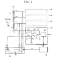
- FIG. 1 illustrates the system configuration of an EL emitting touch switch according to the present invention.
- the EL emitting touch switch of the embodiment comprises a switch body 10, an EL driver (light emission driving means) 20, a timing signal generator (timing signal generating means) 30, and detectors (touch decision means) 40.
- the switch body 10 comprises an EL layer 1, which is a laminate obtained by sandwiching a phosphor layer 1b and an insulating layer 1c between a transparent surface electrode (first electrode) 1a and a back electrode (second electrode) 1d, and a transparent insulating film 6 formed over the EL layer 1.
- the surface electrode 1a serves as both a touch detection electrode and an EL driving electrode.
- the switch body 10 of the embodiment is configured in the form of a panel provided with multiple touch detection electrodes. In other words, multiple surface electrodes 1a are associated with a single back electrode 1d.
- the EL layer 1 is formed with respect to each of the surface electrodes 1a.
- the EL driver 20 includes an AC power supply 21 for outputting a 5-kHz sinusoidal wave voltage of 200 V, for example, and switching elements 22.
- the EL driver 20 has the function of applying a driving voltage between the back electrode 1d and each surface electrode 1a to cause the corresponding EL layer 1 to emit light.
- Each switching element 22 is inserted in a circuit connecting the AC power supply 21 and the corresponding surface electrode 1a to open and close the circuit.
- the EL driver 20 turns on or off the switching element 22 connected to the surface electrode 1a associated with the corresponding EL layer.
- the on/off operation of each switching element 22 is also controlled by a timing signal T1 periodically supplied from the timing signal generator 30.
- T1 periodically supplied from the timing signal generator 30.
- the detector 40 is provided for each of the surface electrodes 1a and has the function of detecting the contact of part of a human body with the corresponding surface electrode 1a. Specifically, the detector 40 determines, based on an input signal (input voltage) S2 from the surface electrode 1a and an input signal (input voltage) S1 from the back electrode 1d, whether or not the corresponding surface electrode 1a is in contact with a human body.
- Each detector 40 comprises a differential amplifier circuit (feedback circuit) including resistors R1 to R4 and an operational amplifier 41, and a decision circuit 42.
- the switching element 22 While the switching element 22 is turned on and thus the corresponding EL layer is emitting light, the S2 input side is grounded and the voltage of the AC power supply 21 is applied only to the S1 input side because of the ON state of the switching element 22.
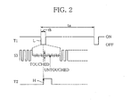
- FIG. 2 is a time chart showing the transition of timing signals T1 and T2 and an output signal S3 of the differential amplifier circuit (output signal of the operational amplifier 41).
- the output signal (output voltage) S3 of the operational amplifier 41 has a large amplitude corresponding to the voltage of the AC power supply 21, as shown in FIG. 2 , the amplitude value being given by the following expression (3):
- S ⁇ 3 S ⁇ 2 - S ⁇ 1 ⁇ R ⁇ 3 / R ⁇ 1
- the timing signal generator 30 outputs, as the timing signal T1, an L signal (OFF signal) which appears at intervals of ta and lasts for a period tb.
- Each switching element 22 is configured so as to be turned off (opened) when supplied with the L signal (OFF signal) from the timing signal generator 30.
- the interval ta and OFF period tb of the timing signal T1 are set to about 50 msec and 2 msec, respectively, but the interval ta and the OFF period tb to be set are not limited to these values and may be set as needed on condition that the relationship tb ⁇ ta is fulfilled.
- the timing signal generator 30 also outputs, as the timing signal T2, an H signal shorter than the OFF period tb to the decision circuit 42. The generation timing (OFF-to-ON transition) of the H signal is set so as to take place while the L signal is being output.
- the back electrode 1d and the surface electrode 1a of the switch body 10 are coupled with large electrostatic capacitance, and accordingly, both the voltage of the back electrode 1d and the voltage of the surface electrode 1a become equal to the voltage of the AC power supply 21.
- the voltage of the output signal S3 of the differential amplifier circuit is therefore 0 V while the switching element 22 is turned off.
- the period for which the output signal S3 remains at 0 V is equal to the period tb for which the timing signal T1 remains low (L signal) but is shown enlarged for the sake of visibility, as indicated by broken lines in the figure.
- the timing signal T2 is also shown on the same time scale as the output signal S3.
- the output signal S3 shows different amplitudes during the OFF period of the switching element 22 depending on whether the surface electrode 1a is touched by the operator or not, as indicated by the solid and broken lines in FIG. 2 . Based on the change in the amplitude, the decision circuit 42 detects the operator's touch.
- the decision circuit 42 includes a detector circuit, not shown, for converting the amplitude of the output signal S3 to direct current (DC) voltage, and compares the DC voltage with a predetermined threshold at the rise timing of the timing signal T2 supplied from the timing signal generator 30. Then, the decision circuit 42 outputs the result of the comparison from a terminal S4, the output being used to control the operation of the corresponding automobile device connected to the detector 40.
- a detector circuit not shown, for converting the amplitude of the output signal S3 to direct current (DC) voltage, and compares the DC voltage with a predetermined threshold at the rise timing of the timing signal T2 supplied from the timing signal generator 30. Then, the decision circuit 42 outputs the result of the comparison from a terminal S4, the output being used to control the operation of the corresponding automobile device connected to the detector 40.
- the potentials of the signals S1 and S2 are kept equal by the feedback current Ib.
- the value of the electrostatic capacitance or impedance does not affect the sensitivity of the detector for detecting the operator's touch, and moreover, the mutual influence of adjacent surface electrodes 1a of the switch body 10 attributable to the electrostatic capacitance or the impedance can be eliminated.
- the EL emitting touch switch of the embodiment includes the multiple surface electrodes 1a, each functioning as both the touch detection electrode and the EL driving electrode, and the single (common) back electrode 1d.
- This configuration makes it possible to eliminate the mutual influence of the surface electrodes caused due to the electrostatic capacitance or impedance present between each of the surface electrodes 1a and the back electrode 1d, and also permits accurate detection of the operator's touch on the individual surface electrode 1a.
Landscapes
- Switches That Are Operated By Magnetic Or Electric Fields (AREA)
- Electronic Switches (AREA)
- Electroluminescent Light Sources (AREA)
- Push-Button Switches (AREA)
- Circuit Arrangement For Electric Light Sources In General (AREA)
- Control Of El Displays (AREA)
Abstract
Description
- This invention relates to EL (electroluminescence) emitting touch switches utilizing EL in combination with a touch switch, and more particularly, to an EL emitting touch switch provided with a plurality of touch detection electrodes.
- Touch switches have been conventionally known which are provided with conductive electrodes for detecting the contact or proximity of part of a human body with or to the electrodes. In such touch switches, the electrode functions as a capacitance sensor, and the on/off operation of the touch switch is detected based on change in the impedance (electrostatic capacitance) of the electrode induced by the contact of a human body with the electrode.
- There have also been known EL emitting touch switches in which the touch switch is combined with an organic or inorganic EL device for emitting light from a phosphor therein so that light may be emitted from the electrode upon detection of the contact of a human body with the electrode. This type of touch switch is disclosed, for example, in Unexamined Japanese Patent Publication No.
H05-135654 -
FIG. 3 is a schematic sectional view of an example of the body of the touch switch disclosed inPatent Document 1. As shown inFIG. 3 , the body of the touch switch has a transparent, electricallyinsulating substrate 2, a transparent electrode 5 formed on a surface (upper surface) of thesubstrate 2, and a transparentinsulating film 6 covering the upper surface of the electrode 5 and forming a touch surface. - Also, an
EL layer 1 is formed on the reverse surface (lower surface) of the transparentinsulating substrate 2. TheEL layer 1 is formed by successively laminating, from the substrate side downward, a transparent electrode 1a, aphosphor layer 1b, aninsulating layer 1c, and aback electrode 1d. When an alternating-current (AC) voltage is applied between the twoelectrodes 1a and 1d, theEL layer 1 emits light. - The emitted light propagates through the transparent electrode 1a, the transparent
insulating substrate 2, the transparent touch detection electrode 5 and the transparentinsulating film 6 to the outside of the touch switch, thus enabling the operator to easily locate the transparentinsulating film 2 with the aid of the emitted light and touch the switch with his/her finger. When the transparentinsulating film 6 is touched with the operator's finger, a touch decision circuit, not shown, connected to the transparent touch detection electrode 5 detects a change of the impedance or capacitance and judges that the transparentinsulating film 6 is touched by the operator. Based on the judgment, the on-off control of a device connected to the touch decision circuit may be executed. - This touch switch essentially requires, however, a pair of
electrodes 1a and 1d for driving theEL layer 1 to emit light, as well as the transparent touch detection electrode 5. It is therefore difficult to reduce the thickness of the touch switch, and also since the number of electrode layers is large, the cost increases. - As a solution to the problem, Japanese Patent No.
3284259 -
FIG. 4 schematically shows the configuration of the EL emitting touch switch disclosed inPatent Document 2. As shown inFIG. 4 , theswitch body 10 of the touch switch includes anEL layer 1, which is a laminate having aphosphor layer 1b and aninsulating layer 1c sandwiched between a transparent electrode (surface electrode) 1a and aback electrode 1d. TheEL layer 1 is formed on aninsulating substrate 3 and covered with a transparentinsulating film 6. The transparent electrode 1a functions as both the touch detection electrode and the EL driving electrode. - Also, to the
switch body 10 are connected atouch decision circuit 100 and anEL driver circuit 200 in parallel with each other. Thetouch decision circuit 100 detects change in potential of the transparent electrode 1a, to thereby detect the contact of part of the operator's body with the transparentinsulating film 6. TheEL driver circuit 200 outputs an AC voltage based on the potential of the transparent electrode 1a, to cause theEL layer 1 to emit light. - The
switch body 10 is further provided with adrive control circuit 300, in addition to thetouch decision circuit 100 and theEL driver circuit 200. Thetouch decision circuit 100 operates in accordance with a control signal from thedrive control circuit 300. Also, thetouch decision circuit 100 is so configured as to detect the contact of the operator's finger with the transparentinsulating film 6 on the basis of change in the difference between the potential VA of the transparent electrode 1a and a ground potential VG. When the operator's touch on thetransparent insulating film 6 is detected by thetouch decision circuit 100, thedrive control circuit 300 drives theEL driver circuit 200 to apply an AC electric field between theelectrodes 1a and 1d, thereby controlling the emission of light from theEL layer 1. - It is conceivable that touch switches such as those described above are applied to a control panel for equipment (specifically, audio equipment or an air conditioner) installed in the passenger compartment of an automobile. With the technique disclosed in
Patent Document 1, however, it is difficult to reduce the thickness of the touch switch, and accordingly, the disclosed touch switch is not suited for use in the control panel of, for example, audio equipment or air conditioner of an automobile. In the case ofPatent Document 2, no problem arises if the touch detection electrode (transparent electrode 1a) used is one in number, but the disclosed technique fails to provide an effective solution in cases where a plurality of touch detection electrodes exist in the same panel, as in a control panel for an automobile device. - Specifically, in an EL panel with many independent light emitting regions (EL layer 1), the
back electrode 1d generally has an area covering all light emitting regions so as to be used as a common electrode. However, where the EL panel is configured in the manner disclosed inPatent Document 2 such that the EL driver circuit is connected to the transparent electrode 1a and theback electrode 1d so as to operate based on the potential of the transparent electrode 1a serving also as the touch detection electrode, that is, the potential of theback electrode 1d is floating with respect to the ground potential, large electrostatic capacitance exists between the transparent electrode 1a, which constitutes an independent light emitting region, and theback electrode 1d. Consequently, when one of the multiple touch detection electrodes is touched by the operator, the touch is detected with respect to all switches at the same time (seeFIG. 5 ). - The present invention was made to solve the above problems, and an object thereof is to provide an EL emitting touch switch which includes a plurality of surface electrodes, each functioning as both a touch detection electrode and an EL driving electrode, and a single (common) back electrode and in which mutual influence of the surface electrodes is eliminated to enable a touch on the individual surface electrode to be detected independently and accurately.
- This object can be achieved by the features defined in the claims.
- Particularly, the present invention provides an EL emitting touch switch characterized by comprising a plurality of first electrodes having light permeability; a second electrode arranged so as to face the plurality of first electrodes, the second electrode functioning as a single electrode associated with the plurality of first electrodes; a plurality of EL layers each sandwiched between a corresponding one of the first electrodes and the second electrode, each of the EL layers being a laminate including a phosphor layer and an electrically insulating layer; light emission driving means arranged for applying a driving voltage between each of the first electrodes and the second electrode to cause the EL layers to emit light; timing signal generating means arranged for generating a timing signal to control the light emission driving means such that the application of the driving voltage is stopped at predetermined intervals; and touch decision means provided for each of the first electrodes, each of the touch decision means including a feedback circuit that supplies an electric current to a corresponding one of the first electrodes such that potentials of the corresponding first electrode and the second electrode become equal to each other, and each of the touch decision means detecting contact of a human body with the corresponding first electrode based on operation of the feedback circuit while the application of the driving voltage by the light emission driving means is stopped in accordance with the timing signal.
- In the EL emitting touch switch according to the present invention, the first electrodes are surface electrodes each functioning as both the touch detection electrode and the EL driving electrode, and the second electrode is a single (common) back electrode. Consequently, the EL emitting touch switch having the multiple surface electrodes is provided. This configuration makes it possible to eliminate the mutual influence of the surface electrodes caused due to the electrostatic capacitance between the surface and back electrodes and, as a consequence, to accurately detect a touch on the individual surface electrode. It is therefore possible to provide an EL emitting touch switch best suited for use in a panel with a plurality of switches, such as a control panel (instrument panel) for a device installed in the passenger compartment of a motor vehicle.
- Preferably, the feedback circuit is a differential amplifier circuit including an operational amplifier and resistors, and each of the touch decision means detects the contact of a human body with the corresponding first electrode based on an output voltage of the operational amplifier.
- With the EL emitting touch switch configured in this manner, electric current can be supplied to the corresponding one of the first electrodes by using a simple circuit configuration so that the potentials of the corresponding first electrode and the second electrode may become equal to each other, thus making it easy to implement the touch decision means.
- According to a preferred embodiment, there is provided an EL emitting touch switch with differential amplifier circuits each including an operational amplifier (41) and resistors (R1, R2, R3, R4) for supplying an electric current to a corresponding surface electrode (1a) so that the potential of the surface electrode (1a) may become equal to that of a back electrode (1d). While the application of a driving voltage to an EL layer (1) is stopped, a corresponding detector (40) of the EL emitting touch switch detects the contact of a human body with the surface electrode (1a) on the basis of the output signal from the operational amplifier (41).
- The present invention will become more fully understood from the detailed description given hereinafter and the accompanying drawings which are given by way of illustration only, and thus, are not limitative of the present invention, and wherein:
-
FIG. 1 shows the configuration of an EL emitting touch switch according to the present invention; -
FIG. 2 is a time chart showing the transition of timing signals and the output signal of a differential amplifier circuit, used in the EL emitting touch switch according to the present invention; -
FIG. 3 is a sectional view of the switch body of a conventional EL emitting touch switch; -
FIG. 4 shows the configuration of another conventional EL emitting touch switch; and -
FIG. 5 illustrates a problem associated with the conventional switch. - A preferred embodiment of the present invention will be hereinafter described with reference to the accompanying drawings.
-
FIG. 1 illustrates the system configuration of an EL emitting touch switch according to the present invention. - As shown in
FIG. 1 , the EL emitting touch switch of the embodiment comprises aswitch body 10, an EL driver (light emission driving means) 20, a timing signal generator (timing signal generating means) 30, and detectors (touch decision means) 40. - Like the
switch body 10 of the conventional touch switch shown inFIG. 4 , theswitch body 10 comprises anEL layer 1, which is a laminate obtained by sandwiching aphosphor layer 1b and aninsulating layer 1c between a transparent surface electrode (first electrode) 1a and a back electrode (second electrode) 1d, and a transparentinsulating film 6 formed over theEL layer 1. The surface electrode 1a serves as both a touch detection electrode and an EL driving electrode. More specifically, theswitch body 10 of the embodiment is configured in the form of a panel provided with multiple touch detection electrodes. In other words, multiple surface electrodes 1a are associated with asingle back electrode 1d. Thus, theEL layer 1 is formed with respect to each of the surface electrodes 1a. - The
EL driver 20 includes anAC power supply 21 for outputting a 5-kHz sinusoidal wave voltage of 200 V, for example, andswitching elements 22. TheEL driver 20 has the function of applying a driving voltage between theback electrode 1d and each surface electrode 1a to cause thecorresponding EL layer 1 to emit light. - Each
switching element 22 is inserted in a circuit connecting theAC power supply 21 and the corresponding surface electrode 1a to open and close the circuit. In compliance with an external requirement (e.g., when the nighttime illumination switch, which is not shown, of an automobile is operated), theEL driver 20 turns on or off theswitching element 22 connected to the surface electrode 1a associated with the corresponding EL layer. The on/off operation of eachswitching element 22 is also controlled by a timing signal T1 periodically supplied from thetiming signal generator 30. Thus, even while theswitching elements 22 are controlled to be turned on in accordance with external requirements, theelements 22 are periodically turned off in response to the timing signal T1. - The
detector 40 is provided for each of the surface electrodes 1a and has the function of detecting the contact of part of a human body with the corresponding surface electrode 1a. Specifically, thedetector 40 determines, based on an input signal (input voltage) S2 from the surface electrode 1a and an input signal (input voltage) S1 from theback electrode 1d, whether or not the corresponding surface electrode 1a is in contact with a human body. Eachdetector 40 comprises a differential amplifier circuit (feedback circuit) including resistors R1 to R4 and anoperational amplifier 41, and adecision circuit 42. The resistance values of the resistors R1 to R4 are set so as to fulfill the relationships indicated by the following expressions (1) and (2):

- While the switching
element 22 is turned on and thus the corresponding EL layer is emitting light, the S2 input side is grounded and the voltage of theAC power supply 21 is applied only to the S1 input side because of the ON state of the switchingelement 22. -
FIG. 2 is a time chart showing the transition of timing signals T1 and T2 and an output signal S3 of the differential amplifier circuit (output signal of the operational amplifier 41). During the application of the voltage from theAC power supply 21, the output signal (output voltage) S3 of theoperational amplifier 41 has a large amplitude corresponding to the voltage of theAC power supply 21, as shown inFIG. 2 , the amplitude value being given by the following expression (3):
- The
timing signal generator 30 outputs, as the timing signal T1, an L signal (OFF signal) which appears at intervals of ta and lasts for a period tb. Each switchingelement 22 is configured so as to be turned off (opened) when supplied with the L signal (OFF signal) from thetiming signal generator 30. Preferably, the interval ta and OFF period tb of the timing signal T1 are set to about 50 msec and 2 msec, respectively, but the interval ta and the OFF period tb to be set are not limited to these values and may be set as needed on condition that the relationship tb < ta is fulfilled. Thetiming signal generator 30 also outputs, as the timing signal T2, an H signal shorter than the OFF period tb to thedecision circuit 42. The generation timing (OFF-to-ON transition) of the H signal is set so as to take place while the L signal is being output. - While the L signal is output (during the OFF period), the
back electrode 1d and the surface electrode 1a of theswitch body 10 are coupled with large electrostatic capacitance, and accordingly, both the voltage of theback electrode 1d and the voltage of the surface electrode 1a become equal to the voltage of theAC power supply 21. The voltage of the output signal S3 of the differential amplifier circuit is therefore 0 V while the switchingelement 22 is turned off. - In
FIG. 2 , the period for which the output signal S3 remains at 0 V is equal to the period tb for which the timing signal T1 remains low (L signal) but is shown enlarged for the sake of visibility, as indicated by broken lines in the figure. The timing signal T2 is also shown on the same time scale as the output signal S3. - When the operator touches the surface electrode 1a, a ground current IS flows through the operator. Accordingly, the potential of the surface electrode 1a tends to lower, developing a potential difference between the input signals S1 and S2. However, the
operational amplifier 41 outputs, through the resistor R3, a feedback current Ib compensating for the potential difference (an imaginary short state of the operational amplifier), with the result that the potential difference between the signals S1 and S2, in other words, between the back andsurface electrodes 1d and 1a is canceled out. At this time, therefore, the voltage of the output signal S3, which is the voltage generated by theoperational amplifier 41 to output the feedback current through the resistor R3, is proportional to the ground current IS flowing through the operator. - Since the
detector 40 operates in the aforementioned manner, the output signal S3 shows different amplitudes during the OFF period of the switchingelement 22 depending on whether the surface electrode 1a is touched by the operator or not, as indicated by the solid and broken lines inFIG. 2 . Based on the change in the amplitude, thedecision circuit 42 detects the operator's touch. - The
decision circuit 42 includes a detector circuit, not shown, for converting the amplitude of the output signal S3 to direct current (DC) voltage, and compares the DC voltage with a predetermined threshold at the rise timing of the timing signal T2 supplied from thetiming signal generator 30. Then, thedecision circuit 42 outputs the result of the comparison from a terminal S4, the output being used to control the operation of the corresponding automobile device connected to thedetector 40. - According to the embodiment configured as described above, while the L signal is being output, the potentials of the signals S1 and S2 are kept equal by the feedback current Ib. In addition, since the resistors fulfill the relationships R1 = R2 and R3 = R4, the potentials of the back and
surface electrodes 1d and 1a also are eventually made equal to each other. Consequently, no electric current flows between the back andsurface electrodes 1d and 1a, no matter what value the electrostatic capacitance or impedance present between theelectrodes 1d and 1a may be, and thus, the value of the electrostatic capacitance or impedance has nothing to do with the magnitude of the output signal S3 that varies when the operator touches the surface electrode 1a. That is to say, the value of the electrostatic capacitance or impedance does not affect the sensitivity of the detector for detecting the operator's touch, and moreover, the mutual influence of adjacent surface electrodes 1a of theswitch body 10 attributable to the electrostatic capacitance or the impedance can be eliminated. - As described above, the EL emitting touch switch of the embodiment includes the multiple surface electrodes 1a, each functioning as both the touch detection electrode and the EL driving electrode, and the single (common)
back electrode 1d. This configuration makes it possible to eliminate the mutual influence of the surface electrodes caused due to the electrostatic capacitance or impedance present between each of the surface electrodes 1a and theback electrode 1d, and also permits accurate detection of the operator's touch on the individual surface electrode 1a. - The invention being thus described, it will be obvious that the same may be varied in many ways. Such variations are not to be regarded as a departure from the spirit and scope of the invention, and all such modifications as would be obvious to one skilled in the art are intended to be included within the scope of the following claims.
Claims (2)
- An EL emitting touch switch, characterized by comprising:a plurality of first electrodes (1a) having light permeability;a second electrode (1d) arranged so as to face the plurality of first electrodes (1a), the second electrode (1d) functioning as a single electrode associated with the plurality of first electrodes (1a);a plurality of EL layers (1) each sandwiched between a corresponding one of the first electrodes (1a) and the second electrode (1d), each of the EL layers (1) being a laminate including a phosphor layer (1b) and an electrically insulating layer (1c);light emission driving means (20) arranged for applying a driving voltage between each of the first electrodes (1a) and the second electrode (1d) to cause the EL layers (1) to emit light;timing signal generating means (30) arranged for generating a timing signal (T1) to control the light emission driving means (20) such that the application of the driving voltage is stopped at predetermined intervals; andtouch decision means (40) provided for each of the first electrodes (1a), each of the touch decision means (40) including a feedback circuit (R1, R2, R3, R4, 41) that supplies an electric current to a corresponding one of the first electrodes (1a) such that potentials of the corresponding first electrode (1a) and the second electrode (1d) become equal to each other, and each of the touch decision means detecting contact of a human body with the corresponding first electrode (1a) based on operation of the feedback circuit (R1, R2, R3, R4, 41) while the application of the driving voltage by the light emission driving means (20) is stopped in accordance with the timing signal (T1).
- The EL emitting touch switch according to claim 1, characterized in that:said feedback circuit is a differential amplifier circuit including an operational amplifier (41) and resistors (R1, R2, R3, R4); andeach of said touch decision means (40) detects the contact of a human body with the corresponding first electrode (1a) based on an output voltage of the operational amplifier (41).
Applications Claiming Priority (1)
| Application Number | Priority Date | Filing Date | Title |
|---|---|---|---|
| JP2007242059A JP4791427B2 (en) | 2007-09-19 | 2007-09-19 | EL light-emitting touch switch |
Publications (4)
| Publication Number | Publication Date |
|---|---|
| EP2040380A2 true EP2040380A2 (en) | 2009-03-25 |
| EP2040380A3 EP2040380A3 (en) | 2014-11-26 |
| EP2040380B1 EP2040380B1 (en) | 2018-10-10 |
| EP2040380B8 EP2040380B8 (en) | 2019-03-06 |
Family
ID=40242717
Family Applications (1)
| Application Number | Title | Priority Date | Filing Date |
|---|---|---|---|
| EP08005164.2A Ceased EP2040380B8 (en) | 2007-09-19 | 2008-03-19 | EL emitting touch switch |
Country Status (6)
| Country | Link |
|---|---|
| US (1) | US8766924B2 (en) |
| EP (1) | EP2040380B8 (en) |
| JP (1) | JP4791427B2 (en) |
| KR (1) | KR100992278B1 (en) |
| CN (1) | CN101394175B (en) |
| RU (1) | RU2389132C2 (en) |
Cited By (1)
| Publication number | Priority date | Publication date | Assignee | Title |
|---|---|---|---|---|
| EP2290493A3 (en) * | 2009-08-27 | 2014-09-03 | LG Electronics Inc. | Mobile terminal |
Families Citing this family (9)
| Publication number | Priority date | Publication date | Assignee | Title |
|---|---|---|---|---|
| CN106020583B (en) | 2009-08-21 | 2019-05-28 | 苹果公司 | Method and apparatus for capacitance sensing |
| KR101588450B1 (en) * | 2009-10-23 | 2016-01-25 | 엘지디스플레이 주식회사 | Touch Sensor Insel Type Organic Light Emitting Diode |
| JP5766928B2 (en) * | 2010-09-29 | 2015-08-19 | 株式会社ジャパンディスプレイ | Display device with touch detection function and electronic device |
| KR101202745B1 (en) | 2011-04-21 | 2012-11-19 | 주식회사 실리콘웍스 | Touch sensing circuit |
| JP6096421B2 (en) * | 2012-05-07 | 2017-03-15 | 拓夫 高井 | Touch switch input device |
| US9035894B2 (en) * | 2013-01-24 | 2015-05-19 | Industrial Technology Research Institute | Touch sensing and feedback apparatuses and methods |
| CN105493626B (en) * | 2014-06-06 | 2017-05-03 | 柯尼卡美能达株式会社 | Organic electroluminescence module, smart device and lighting device |
| EP3187983A4 (en) * | 2014-08-25 | 2018-04-18 | Konica Minolta, Inc. | Organic electroluminescent module, smart device, and illumination apparatus |
| WO2016181704A1 (en) * | 2015-05-13 | 2016-11-17 | コニカミノルタ株式会社 | Organic electroluminescence module and smart device |
Citations (2)
| Publication number | Priority date | Publication date | Assignee | Title |
|---|---|---|---|---|
| JPH05135654A (en) | 1991-11-14 | 1993-06-01 | Matsushita Electric Ind Co Ltd | EL illuminated switch |
| JP3284259B2 (en) | 1996-03-14 | 2002-05-20 | 松下電工株式会社 | EL illuminated touch switch |
Family Cites Families (20)
| Publication number | Priority date | Publication date | Assignee | Title |
|---|---|---|---|---|
| DE2626927B2 (en) * | 1976-06-16 | 1981-02-19 | Bodenseewerk Perkin-Elmer & Co Gmbh, 7770 Ueberlingen | Circuit for converting an alternating voltage into a direct voltage |
| GB2059657B (en) * | 1977-07-30 | 1982-12-01 | Ti Group Services Ltd | Supervision of touch control switches |
| JPS6025851B2 (en) * | 1978-04-11 | 1985-06-20 | 株式会社日立製作所 | Display element drive circuit |
| JPS5528247A (en) * | 1978-08-21 | 1980-02-28 | Hitachi Ltd | El element drive circuit |
| US4740781A (en) * | 1985-02-08 | 1988-04-26 | Itt Gilfillan | Touch panel data entry device for thin film electroluminescent panels |
| JP2969760B2 (en) * | 1990-03-30 | 1999-11-02 | 株式会社島津製作所 | Patient transfer device |
| US5572205A (en) * | 1993-03-29 | 1996-11-05 | Donnelly Technology, Inc. | Touch control system |
| KR100300397B1 (en) | 1994-04-21 | 2001-10-22 | 김순택 | System having touch panel and digitizer function and driving method |
| JP3473303B2 (en) * | 1996-12-24 | 2003-12-02 | 松下電工株式会社 | Illuminated touch switch device |
| JP3394187B2 (en) * | 1997-08-08 | 2003-04-07 | シャープ株式会社 | Coordinate input device and display integrated type coordinate input device |
| JP2000150144A (en) * | 1998-11-11 | 2000-05-30 | Citizen Electronics Co Ltd | EL inverter using simulated inductor |
| TW507158B (en) * | 2001-01-05 | 2002-10-21 | Darfon Electronics Corp | Detecting device and method of mouse touch pad |
| KR100642183B1 (en) * | 2001-08-22 | 2006-11-06 | 샤프 가부시키가이샤 | Touch sensor, display device with touch sensor, and location data generation method |
| JP2003075547A (en) * | 2001-09-04 | 2003-03-12 | Matsushita Electric Ind Co Ltd | Object detection device |
| KR100449745B1 (en) * | 2002-11-21 | 2004-09-22 | 삼성전자주식회사 | Apparatus and Method for avoiding noise of touch screen |
| US7626575B2 (en) * | 2003-03-28 | 2009-12-01 | Samsung Electronics Co., Ltd. | Light pen |
| JP2005166939A (en) * | 2003-12-02 | 2005-06-23 | Sumitomo Electric Ind Ltd | Semiconductor light emitting device driving circuit |
| US7221359B2 (en) * | 2004-03-17 | 2007-05-22 | Lear Corporation | Illuminated touch switch |
| KR100460194B1 (en) * | 2004-07-22 | 2004-12-04 | (주)디지텍시스템스 | Device for controlling touch panel |
| JP2006313709A (en) * | 2005-05-09 | 2006-11-16 | Hosiden Corp | El illumination type switch |
-
2007
- 2007-09-19 JP JP2007242059A patent/JP4791427B2/en not_active Expired - Fee Related
-
2008
- 2008-03-14 US US12/076,207 patent/US8766924B2/en not_active Expired - Fee Related
- 2008-03-19 EP EP08005164.2A patent/EP2040380B8/en not_active Ceased
- 2008-04-01 KR KR1020080030101A patent/KR100992278B1/en not_active Expired - Fee Related
- 2008-06-20 RU RU2008125131/09A patent/RU2389132C2/en active
- 2008-06-23 CN CN2008101252540A patent/CN101394175B/en not_active Expired - Fee Related
Patent Citations (2)
| Publication number | Priority date | Publication date | Assignee | Title |
|---|---|---|---|---|
| JPH05135654A (en) | 1991-11-14 | 1993-06-01 | Matsushita Electric Ind Co Ltd | EL illuminated switch |
| JP3284259B2 (en) | 1996-03-14 | 2002-05-20 | 松下電工株式会社 | EL illuminated touch switch |
Cited By (2)
| Publication number | Priority date | Publication date | Assignee | Title |
|---|---|---|---|---|
| EP2290493A3 (en) * | 2009-08-27 | 2014-09-03 | LG Electronics Inc. | Mobile terminal |
| US9244534B2 (en) | 2009-08-27 | 2016-01-26 | Lg Electronics Inc. | Mobile terminal |
Also Published As
| Publication number | Publication date |
|---|---|
| RU2008125131A (en) | 2009-12-27 |
| KR100992278B1 (en) | 2010-11-05 |
| CN101394175A (en) | 2009-03-25 |
| EP2040380B8 (en) | 2019-03-06 |
| US20090073133A1 (en) | 2009-03-19 |
| RU2389132C2 (en) | 2010-05-10 |
| EP2040380A3 (en) | 2014-11-26 |
| KR20090030194A (en) | 2009-03-24 |
| JP4791427B2 (en) | 2011-10-12 |
| CN101394175B (en) | 2012-01-18 |
| EP2040380B1 (en) | 2018-10-10 |
| US8766924B2 (en) | 2014-07-01 |
| JP2009076237A (en) | 2009-04-09 |
Similar Documents
| Publication | Publication Date | Title |
|---|---|---|
| EP2040380B1 (en) | EL emitting touch switch | |
| US8638314B2 (en) | Capacitive touch buttons combined with electroluminescent lighting | |
| US7910842B2 (en) | EL light emitting touch switch | |
| US20100295604A1 (en) | Oled illumination device with integrated proximity sensor | |
| KR102811755B1 (en) | Touch sensor and display device having the touch sensor | |
| US20060185968A1 (en) | Seat control system | |
| JP2016120890A (en) | Vehicular switching device | |
| US20070018998A1 (en) | Poster with electronic touchpad input areas | |
| JPH09251820A (en) | El light emission type touch switch | |
| KR100891223B1 (en) | Input device, electronic device and control method of input device | |
| EP3514452B1 (en) | Illuminating device | |
| US10120492B2 (en) | Touch sensor and information processing system | |
| JP5490043B2 (en) | Occupant detection device | |
| CN118519545A (en) | Detecting user input in a vehicle with integrated capacitive compensation | |
| US20240118759A1 (en) | Touch display | |
| US20070068786A1 (en) | Touch pad having integrated lighting feature and touch sensor and method of operating the same | |
| CN110418730A (en) | Display element and device for running display element | |
| KR20170104857A (en) | Touch pressure detecting IC using mutual method | |
| JP2023154468A (en) | display input device | |
| WO2024194601A1 (en) | Touch-sensitive apparatus having a touch sensor and display element and method of operating such |
Legal Events
| Date | Code | Title | Description |
|---|---|---|---|
| PUAI | Public reference made under article 153(3) epc to a published international application that has entered the european phase |
Free format text: ORIGINAL CODE: 0009012 |
|
| 17P | Request for examination filed |
Effective date: 20080319 |
|
| AK | Designated contracting states |
Kind code of ref document: A2 Designated state(s): AT BE BG CH CY CZ DE DK EE ES FI FR GB GR HR HU IE IS IT LI LT LU LV MC MT NL NO PL PT RO SE SI SK TR |
|
| AX | Request for extension of the european patent |
Extension state: AL BA MK RS |
|
| PUAL | Search report despatched |
Free format text: ORIGINAL CODE: 0009013 |
|
| AK | Designated contracting states |
Kind code of ref document: A3 Designated state(s): AT BE BG CH CY CZ DE DK EE ES FI FR GB GR HR HU IE IS IT LI LT LU LV MC MT NL NO PL PT RO SE SI SK TR |
|
| AX | Request for extension of the european patent |
Extension state: AL BA MK RS |
|
| RIC1 | Information provided on ipc code assigned before grant |
Ipc: H03K 17/96 20060101AFI20141022BHEP |
|
| RBV | Designated contracting states (corrected) |
Designated state(s): AT BE BG CH CY CZ DE DK EE ES FI FR GB GR HR HU IE IS IT LI LT LU LV MC MT NL NO PL PT RO SE SI SK TR |
|
| RBV | Designated contracting states (corrected) |
Designated state(s): AT BE BG CH CY CZ DE DK EE ES FI FR GB GR HR HU IE IS IT LI LT LU LV MC MT NL NO PL PT RO SE SI SK TR |
|
| AKX | Designation fees paid |
Designated state(s): DE FR GB |
|
| AXX | Extension fees paid |
Extension state: RS Extension state: AL Extension state: MK Extension state: BA |
|
| GRAP | Despatch of communication of intention to grant a patent |
Free format text: ORIGINAL CODE: EPIDOSNIGR1 |
|
| INTG | Intention to grant announced |
Effective date: 20180423 |
|
| GRAS | Grant fee paid |
Free format text: ORIGINAL CODE: EPIDOSNIGR3 |
|
| GRAA | (expected) grant |
Free format text: ORIGINAL CODE: 0009210 |
|
| AK | Designated contracting states |
Kind code of ref document: B1 Designated state(s): DE FR GB |
|
| REG | Reference to a national code |
Ref country code: GB Ref legal event code: FG4D |
|
| RIN1 | Information on inventor provided before grant (corrected) |
Inventor name: YAMAUCHI, KAZUTO Inventor name: MURAYAMA, YASUNORI Inventor name: TANAKA, SADAHIKO Inventor name: YAMANOUE, KOUICHI Inventor name: TAKIZAWA, KEITARO |
|
| REG | Reference to a national code |
Ref country code: DE Ref legal event code: R096 Ref document number: 602008057308 Country of ref document: DE |
|
| RAP2 | Party data changed (patent owner data changed or rights of a patent transferred) |
Owner name: MITSUBISHI JIDOSHA KOGYO KABUSHIKI KAISHA |
|
| RAP2 | Party data changed (patent owner data changed or rights of a patent transferred) |
Owner name: MITSUBISHI JIDOSHA KOGYO KABUSHIKI KAISHA |
|
| REG | Reference to a national code |
Ref country code: DE Ref legal event code: R097 Ref document number: 602008057308 Country of ref document: DE |
|
| PLBE | No opposition filed within time limit |
Free format text: ORIGINAL CODE: 0009261 |
|
| STAA | Information on the status of an ep patent application or granted ep patent |
Free format text: STATUS: NO OPPOSITION FILED WITHIN TIME LIMIT |
|
| 26N | No opposition filed |
Effective date: 20190711 |
|
| GBPC | Gb: european patent ceased through non-payment of renewal fee |
Effective date: 20190319 |
|
| PG25 | Lapsed in a contracting state [announced via postgrant information from national office to epo] |
Ref country code: GB Free format text: LAPSE BECAUSE OF NON-PAYMENT OF DUE FEES Effective date: 20190319 |
|
| PGFP | Annual fee paid to national office [announced via postgrant information from national office to epo] |
Ref country code: FR Payment date: 20210210 Year of fee payment: 14 |
|
| PGFP | Annual fee paid to national office [announced via postgrant information from national office to epo] |
Ref country code: DE Payment date: 20210310 Year of fee payment: 14 |
|
| REG | Reference to a national code |
Ref country code: DE Ref legal event code: R119 Ref document number: 602008057308 Country of ref document: DE |
|
| PG25 | Lapsed in a contracting state [announced via postgrant information from national office to epo] |
Ref country code: FR Free format text: LAPSE BECAUSE OF NON-PAYMENT OF DUE FEES Effective date: 20220331 Ref country code: DE Free format text: LAPSE BECAUSE OF NON-PAYMENT OF DUE FEES Effective date: 20221001 |