EP2040378A1 - Semiconductor integrated circuit device - Google Patents
Semiconductor integrated circuit device Download PDFInfo
- Publication number
- EP2040378A1 EP2040378A1 EP06780693A EP06780693A EP2040378A1 EP 2040378 A1 EP2040378 A1 EP 2040378A1 EP 06780693 A EP06780693 A EP 06780693A EP 06780693 A EP06780693 A EP 06780693A EP 2040378 A1 EP2040378 A1 EP 2040378A1
- Authority
- EP
- European Patent Office
- Prior art keywords
- connecting part
- electrostatic capacitance
- power supply
- capacitance element
- gate control
- Prior art date
- Legal status (The legal status is an assumption and is not a legal conclusion. Google has not performed a legal analysis and makes no representation as to the accuracy of the status listed.)
- Granted
Links
Images



Classifications
-
- H—ELECTRICITY
- H03—ELECTRONIC CIRCUITRY
- H03K—PULSE TECHNIQUE
- H03K17/00—Electronic switching or gating, i.e. not by contact-making and –breaking
- H03K17/51—Electronic switching or gating, i.e. not by contact-making and –breaking characterised by the components used
- H03K17/56—Electronic switching or gating, i.e. not by contact-making and –breaking characterised by the components used by the use, as active elements, of semiconductor devices
- H03K17/687—Electronic switching or gating, i.e. not by contact-making and –breaking characterised by the components used by the use, as active elements, of semiconductor devices the devices being field-effect transistors
- H03K17/6871—Electronic switching or gating, i.e. not by contact-making and –breaking characterised by the components used by the use, as active elements, of semiconductor devices the devices being field-effect transistors the output circuit comprising more than one controlled field-effect transistor
- H03K17/6874—Electronic switching or gating, i.e. not by contact-making and –breaking characterised by the components used by the use, as active elements, of semiconductor devices the devices being field-effect transistors the output circuit comprising more than one controlled field-effect transistor in a symmetrical configuration
-
- H—ELECTRICITY
- H02—GENERATION; CONVERSION OR DISTRIBUTION OF ELECTRIC POWER
- H02M—APPARATUS FOR CONVERSION BETWEEN AC AND AC, BETWEEN AC AND DC, OR BETWEEN DC AND DC, AND FOR USE WITH MAINS OR SIMILAR POWER SUPPLY SYSTEMS; CONVERSION OF DC OR AC INPUT POWER INTO SURGE OUTPUT POWER; CONTROL OR REGULATION THEREOF
- H02M3/00—Conversion of DC power input into DC power output
- H02M3/02—Conversion of DC power input into DC power output without intermediate conversion into AC
- H02M3/04—Conversion of DC power input into DC power output without intermediate conversion into AC by static converters
- H02M3/06—Conversion of DC power input into DC power output without intermediate conversion into AC by static converters using resistors or capacitors, e.g. potential divider
- H02M3/07—Conversion of DC power input into DC power output without intermediate conversion into AC by static converters using resistors or capacitors, e.g. potential divider using capacitors charged and discharged alternately by semiconductor devices with control electrode, e.g. charge pumps
-
- H—ELECTRICITY
- H03—ELECTRONIC CIRCUITRY
- H03K—PULSE TECHNIQUE
- H03K17/00—Electronic switching or gating, i.e. not by contact-making and –breaking
- H03K17/06—Modifications for ensuring a fully conducting state
- H03K17/063—Modifications for ensuring a fully conducting state in field-effect transistor switches
-
- H—ELECTRICITY
- H03—ELECTRONIC CIRCUITRY
- H03K—PULSE TECHNIQUE
- H03K17/00—Electronic switching or gating, i.e. not by contact-making and –breaking
- H03K17/10—Modifications for increasing the maximum permissible switched voltage
- H03K17/102—Modifications for increasing the maximum permissible switched voltage in field-effect transistor switches
-
- H—ELECTRICITY
- H03—ELECTRONIC CIRCUITRY
- H03K—PULSE TECHNIQUE
- H03K17/00—Electronic switching or gating, i.e. not by contact-making and –breaking
- H03K17/51—Electronic switching or gating, i.e. not by contact-making and –breaking characterised by the components used
- H03K17/56—Electronic switching or gating, i.e. not by contact-making and –breaking characterised by the components used by the use, as active elements, of semiconductor devices
- H03K17/687—Electronic switching or gating, i.e. not by contact-making and –breaking characterised by the components used by the use, as active elements, of semiconductor devices the devices being field-effect transistors
- H03K17/693—Switching arrangements with several input- or output-terminals, e.g. multiplexers, distributors
-
- H—ELECTRICITY
- H02—GENERATION; CONVERSION OR DISTRIBUTION OF ELECTRIC POWER
- H02M—APPARATUS FOR CONVERSION BETWEEN AC AND AC, BETWEEN AC AND DC, OR BETWEEN DC AND DC, AND FOR USE WITH MAINS OR SIMILAR POWER SUPPLY SYSTEMS; CONVERSION OF DC OR AC INPUT POWER INTO SURGE OUTPUT POWER; CONTROL OR REGULATION THEREOF
- H02M3/00—Conversion of DC power input into DC power output
- H02M3/02—Conversion of DC power input into DC power output without intermediate conversion into AC
- H02M3/04—Conversion of DC power input into DC power output without intermediate conversion into AC by static converters
- H02M3/06—Conversion of DC power input into DC power output without intermediate conversion into AC by static converters using resistors or capacitors, e.g. potential divider
- H02M3/07—Conversion of DC power input into DC power output without intermediate conversion into AC by static converters using resistors or capacitors, e.g. potential divider using capacitors charged and discharged alternately by semiconductor devices with control electrode, e.g. charge pumps
- H02M3/072—Conversion of DC power input into DC power output without intermediate conversion into AC by static converters using resistors or capacitors, e.g. potential divider using capacitors charged and discharged alternately by semiconductor devices with control electrode, e.g. charge pumps adapted to generate an output voltage whose value is lower than the input voltage
Definitions
- the present invention relates to a technique for providing a power supply by a switching circuit, and particularly to a technique effectively applied to provide a power supply of a floating power supply by a switching circuit.
- Non-Patent Document 1 As an object of establishing a LAN (Local Area Network) of an airbag system in an automobile, LAN protocols established by Safe-by-Wire Plus consortium and ISO (International Organization for Standardization)/IEC (International Electrotechnical Commission) are known (see Non-Patent Document 1 and Non-Patent Document 2).
- ISO International Organization for Standardization
- ISO International Electrotechnical Commission
- the above-described standards define common specifications for an airbag control unit, a communication protocol between controllers which controls a peripheral device such as an airbag and a seatbelt, and a driver unit which drives a bus, and the requisite minimum specifications are determined.
- the airbag control unit serving as a controller which controls the bus is called a "master", and a side of controlling the peripheral device such as an airbag and a seatbelt is called a "slave".
- the bus connects two lines of the master and the slave and becomes a path for providing the power supply and an operation of a bidirectional communication from a bus interface of the master side to a bus interface of the slave.
- a floating switch unit is used in the bus interface so that communication can be continued even when one side of the buses is short-circuited to a battery (power supply voltage) or a ground potential (reference potential).
- the configuration is operated so that a voltage differential between the buses (the bus A - the bus B) is always maintained.
- the floating switch unit comprises, for example, a switch which charges a first electrostatic capacitance from a battery power supply, a switch which provides the power supply from the first electrostatic capacitance to a transmitter circuit and the like, a switch which provides the power supply from the first electrostatic capacitance to the bus, a switch which charges a second electrostatic capacitance from the battery power supply, a switch which provides the power supply from the second electrostatic capacitance to a bus driver, and others.
- the above-described floating switch unit is required a MOS (Metal Oxide Semiconductor) transistor with high breakdown voltage, an element area of the transistor configuring the switch is comparatively large.
- MOS Metal Oxide Semiconductor
- the required current value is different depending on the number or the type of the slave connected to the bus.
- the current has to be increased in order to enable a plurality of connection, therefore, it can be easily expected that the chip area occupied by a transistor element is further increased in order to decrease the ON-resistance of the switch.
- An object of the present invention is to provide a technique which considerably reduces the number of switches in a switching circuit which provides a floating power supply and achieves downsizing and low-cost of a semiconductor integrated circuit device.
- the present invention includes a semiconductor integrated circuit device having two externally-connected buses and a switching circuit providing the power supply voltage to an arbitrary internal peripheral circuit, wherein the switching circuit comprises: a first switch unit connecting, to an externally-connected a first electrostatic capacitance element, the power supply voltage provided from the battery; a second switch unit providing a electrostatic capacitance charged in a second electrostatic capacitance element to the bus; and a third switch unit charging the electrostatic capacitance in the first electrostatic capacitance element to the second electrostatic capacitance element and providing the power supply to the internal peripheral circuit.
- the present invention comprises in which the first switch unit comprising a first Hi-side switch portion in which a one connecting part thereof is connected to the battery power supply side and the other connecting part thereof is connected to a one connecting part of the first electrostatic capacitance element and comprising a first Lo-side switch portion in which a one connecting part thereof is connected to the battery reference potential side and the other connecting part thereof is connected to the other connecting part of the first electrostatic capacitance element, the second switch unit comprising a second Hi-side switch portion in which a one connecting part thereof is connected to a one connecting part of the first electrostatic capacitance element and the other connecting part thereof is connected to one of the buses and comprising a second Lo-side switch portion in which a one connecting part thereof is connected to the other connecting part of the first electrostatic capacitance element and the other connecting part thereof is connected to the other of the buses, and the third switch unit comprising a third Hi-side switch portion in which a one connecting part thereof is connected to a one connecting part of the first electrostatic capacitance element and the other
- the present invention comprises the first switch unit comprising the first Hi-side switch portion in which a one connecting part thereof is connected to the battery power supply side and the other connecting part thereof is connected to a one junction part of the first electrostatic capacitance element and comprising the first Lo-side switch portion in which a one connecting part thereof is connected to the battery reference potential side and the other connecting part thereof is connected to the other connecting part of the first electrostatic capacitance element, the third switch unit comprising the third Hi-side switch portion in which a one connecting part thereof is connected to a one connecting part of the first electrostatic capacitance element and the other connecting part thereof is connected to a one connecting part of the second electrostatic capacitance element and comprising the third Lo-side switch portion in which a one connecting part thereof is connected to the other connecting part of the first electrostatic capacitance element and the other connecting part thereof is connected to the other connecting part of the second electrostatic capacitance element, and the second switch unit comprising the second Hi-side switch portion in which a one connecting part thereof is connected to a one connecting part thereof
- the present invention comprises each of the first to third Hi-side switch portions comprising first and second transistors connected in series and comprising a P-channel MOS operating as a switch and comprising a first gate control unit generating a gate control signal from an inputted control signal and driving and controlling the first transistor by the gate control signal and comprising a second gate control unit outputting the gate control signal from an inputted control signal and driving and controlling the second transistor by the gate control signal and comprising a first power supply generating unit generating a power supply voltage by which the first gate control unit is operated and comprising a second power supply generating unit generating a power supply voltage by which the second gate control unit is operated, and each of the first to third Lo-side switch portions comprising third and fourth MOS transistors connected in series and operating as a switch and comprising a third gate control unit generating a gate control signal from an inputted control signal and driving and controlling the third transistor by the gate control signal and comprising a fourth gate control unit generating a gate control signal from an inputted control signal and driving and controlling and controlling
- the present invention comprises the first to fourth gate control units comprising level shift units which level-shift the inputted control signals, to convert them to voltage levels for driving the first to fourth transistors, and output them and driver units which generate the gate control signals driving the first to fourth transistors from the signals outputted from the level shift units, and output them.
- the present invention comprises the driver units each has a configuration in which two invertors are connected in series.
- the present invention comprises in which the first to fourth power supply generating units are provided with Zener diodes connected between the power supply voltages provided from the battery, and the power supply voltages which generate, as references, Zener voltages of the Zener diodes are provided to the first to fourth gate control units.
- the present invention comprises in which the first to fourth power supply generating units are provided with: first Zener diodes whose cathodes are connected to the power supply side of the battery; second Zener diodes whose cathodes are connected to anodes of the first Zener diodes and anodes are connected to the reference potential side of the battery; and switches connected between the anodes and the cathodes of the second Zener diodes; and the switches become non-conductive states in performing acceleration tests of gate breakdown voltages in the first to fourth transistors.
- a semiconductor integrated circuit device 1 is used for an airbag system of an automobile and is used as a communication device which controls a bus in the LAN protocol of Automotive Safety Restraints BUS (ASRB) 2.0.
- ASRB Automotive Safety Restraints BUS
- the semiconductor integrated circuit device 1 comprises a control unit 2, a level shift 3, a floating control circuit 4, a transmitter circuit 5, a receiver circuit 6, and a floating switch unit 7.
- a slave unit SU which controls a peripheral device such as an airbag and a seatbelt is connected to the buses A and B.
- the floating control circuit 4 the transmitter circuit 5, and the receiver circuit 6 which are an internal peripheral circuit, the floating power supply is connected so as to be provided from the floating switch unit 7.
- An MCU Micro Controller Unit which controls the entire airbag system through a control terminal is connected to the control unit 2. And a power supply voltage provided from an automobile battery BAT or the like is connected to the control unit 2, the level shift 3, and the floating switch unit 7 so as to be provided. Electrostatic capacitance elements CS and CH are connected externally to the floating switch unit 7, respectively.
- the control unit 2 performs all control of the semiconductor integrated circuit device 1.
- the level shift 3 is an interface which performs a level conversion of a signal transmitted and received between the floating control circuit 4 operated by the floating power supply and the control unit 2 operated by the power supply voltage provided from the automobile battery BAT or the like.
- the floating control circuit 4 performs a switching control of the floating switch unit 7 and controls a transmission/reception signal inputted from and outputted to the buses A and B through the transmitter circuit 5 and the receiver circuit 6.
- the transmitter circuit 5 controls the voltage between the buses A and B, and the receiver circuit 6 determines the voltage level between the buses A and B.
- the floating switch unit 7 charges the electrostatic capacitance elements CS and CH by power supply provided from the battery BAT, provides power supply to the buses A and B and at the same time provides power supply to the floating control circuit 4, the transmitter circuit 5, and the receiver circuit 6 which operate as the floating circuit.
- the plurality of slave units SU on a slave side are connected to the buses A and B as described above, and communication is established through the buses A and B.
- the power phase is used for providing power supply from the master to the slave, and the data phase is used for transmission/reception of data.
- the data is determined by a voltage level difference between the buses A and B (bus A - bus B) of the two lines.
- the voltage level difference when it is at a voltage VP or more, it is regarded as the power phase, and when being at a lower voltage level than that, it is regarded as the data phase.
- '0' is determined at a voltage V0
- '1' is determined at a voltage V1 which is lower than the voltage V0.
- a level at a voltage V1S0 which is lower than the voltage V1 is a special level and is used, for example, for ordering ignition of an airbag and the like.
- the bus interface part which comprises the floating control unit 4, the transmitter circuit 5, the receiver circuit 6 and the like, becomes a floating circuit so that communication can be continued even when either one of the buses A and B is short-circuited to the power supply side of the battery BAT or a ground potential GND serving as a reference potential.
- the bus A is short-circuited to the battery, as shown in FIG. 3
- the voltage level of the bus B is shifted to the battery voltage side
- the voltage level of the bus A is shifted to the ground potential GND side, whereby the buses operate so that a voltage difference of the buses (BUS A - BUS B) is always maintained.
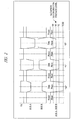
- FIG. 5 is an explanatory diagram showing a configuration example of the floating switch unit 7.
- CL represents a bus load capacitance
- ZL represents a bus load impedance.
- the floating switch unit 7 comprises: switch portions SW1H and SW1L configuring a first switch unit; switch portions SW2H and SW2L configuring a second switch unit; and switch portions SW3H and SW3L configuring a third switch unit.
- the switch portion SW1H as a first Hi-side switch unit and the switch portion SW1L as a first Lo-side switch unit function as a switch for performing charges from the battery BAT to the electrostatic capacitance element CS.
- the switch portion SW2H as a second Hi-side switch unit and the switch portion SW2L as a second Lo-side switch unit function as a switch for performing charges from the electrostatic capacitance element CS as a first electrostatic capacitance element to the electrostatic capacitance element CH as a second electrostatic capacitance element.
- the switch portion SW3H as a third Hi-side switch unit and the switch portion SW3L as a third Lo-side switch unit function as a switch which connects the electrostatic capacitance element CS to each of the buses A and B.
- a one connecting part of the switch portion SW1H is connected to a power supply terminal VBAT, and a one connecting part of the switch portion SW1L is connected to a ground potential terminal GD.
- the battery BAT is connected externally through the power supply terminal VBAT and the ground potential terminal GD.
- the other connecting part of the switch portion SW1H is connected to a one connecting part of the switch portion SW2H, SW3L and a capacitance terminal CS1, respectively.
- the other connecting part of the switch portion SW1L is connected to a one connecting part of the switch portion SW2L, SW3H and a capacitance terminal CS2, respectively.
- the electrostatic capacitance element CS is connected externally to the capacitance terminals CS1 and CS2.
- a bus terminal B1 is connected to the other connecting part of the switch portion SW2H, and a bus terminal B2 is connected to the other connecting part of the switch portion SW2L, and the buses A and B are connected to the bus terminals B1 and B2, respectively.
- the capacitance terminal CS1 is connected to the other connecting part of the switch portion SW3H, and the capacitance terminal CS2 is connected to the other connecting part of the switch portion SW3L.
- the electrostatic capacitance element CH is connected externally to the capacitance terminals CS1 and CS2.
- the other connecting parts of the switch portions SW3H and SW3L are connected respectively so that the power supply voltage is provided as a floating power supply to the floating control circuit 4, the transmitter circuit 5, and the receiver circuit 6.
- the power phase and the data phase are repeated.
- the switch portions SW2H and SW2L and the switch portions SW3H and SW3L are turned ON (conductive state) respectively, and the switch portions SW1H and SW1L are turned OFF (non-conductive state), and the floating power supply is provided from the electrostatic capacitance element CS to each of the buses A and B, the floating control circuit 4, the transmitter circuit 5, and the receiver circuit 6.
- the switch portions SW1H and SW1L are turned ON, and the switch portions SW2H, SW2L, SW3H, and SW3L are turned OFF.
- the electrostatic capacitance element CS is charged by the power supply of the battery BAT, and the electrostatic capacitance element CH provides the floating power supply to each of the floating control circuit 4, the transmitter circuit 5, and the receiver circuit 6.
- the switch portions SW3H and SW3L are turned ON, thereby performing charges from the electrostatic capacitance element CS to the electrostatic capacitance element CH and at the same time providing the power supply voltage to each of the floating control circuit 4, the transmitter circuit 5, and the receiver circuit 6. And, when the power supply is turned ON, since providing the power supply is not performed to the buses A and B, the switch portions SW3H and SW3L are turned OFF.
- the floating switch unit 7 in which the number of switch portions is significantly reduced can be configured.
- ON-resistance of each of the switch portions can be increased, whereby the switch portions can be downsized.
- the switch portion SW1H comprises: voltage generating units 8 and 9; gate control units 10 and 11; and transistors 12 and 13 which comprise P-channel MOSs and serve as first and second MOS transistors.
- the switch portion SW1L comprises: voltage generating units 14 and 15; gate control units 16 and 17; and transistors 18 and 19 which comprise N-channel MOSs and serve as third and fourth MOS transistors.
- the voltage generating units 8 and 9 generate operation voltages which are provided from the power supply voltage of the battery BAT to the gate control units 10 and 11, respectively.
- output parts of the power supply provided from the voltage generating units 8 and 9 to the gate control units 10 and 11 are a NODE b' and a NODE outb', respectively.
- the voltage generating units 14 and 15 generate the operating voltages which are provided from the power supply voltage of the battery BAT to the gate control units 16 and 17, respectively.
- output parts of the power supply provided from the voltage generating units 14 and 15 to the gate control units 16 and 17 are a NODE a' and a NODE outa', respectively.
- the gate control units 8 and 9 output, based on the control signal outputted from the floating control unit 4, the gate control signal, which drives the transistors 12 and 13, to the gate of the transistors 12 and 13, respectively.
- the transistors 12 and 13 are connected in series between the NODE a and the NODE outa shown in FIG. 5 .
- the gate control units 16 and 17 output, based on the control signal outputted from the floating control unit 4, the gate control signal, which drives the transistors 18 and 19, to gates of the transistors 18 and 19, respectively.
- the transistors 18 and 19 are connected in series between the NODE b and the NODE outb shown in FIG. 5 .
- FIG. 6 the configuration example of the switch portion SW1H and the switch portion SW1L has been shown.
- the configurations of the switch portion SW2H, SW3H, SW2L, and SW3L are also similar to configurations shown by FIG. 6 .
- FIG. 7 is an explanatory diagram showing a configuration example of the voltage generating unit 7 and the gate control unit 9 in the switch portion SW1H.
- the voltage generation unit 8 comprises a Zener diode 20 and P-type transistors 21 and 22 composed of bipolars
- the gate control unit 10 comprises a level shifter 23 and inverters 24 and 25.
- a cathode of the Zener diode 20 is connected to the NODE a, and an anode of the Zener diode 20 is connected to the NODE b.
- the anode of the Zener diode 20 is connected to a base of the transistor 22.
- a base of the transistor 21 is connected to an emitter of the transistor 22.
- Each collector of the transistors 21 and 22 is connected to the NODE b.
- An emitter of the transistor 21 is connected to the NODE b'.
- a control signal outputted from the floating control unit 4 is connected so as to be inputted.
- the inverters 24 and 25 are configured to be connected in series.
- the voltage level between the NODE a and the NODE b' that is, such a power supply voltage that a Zener voltage of the Zener diode 20 is generated as a reference is connected.
- control signal outputted from the floating control unit 4 is converted in voltage level by the level shifter 23, and then, through the inverters 24 and 25, is outputted as a gate control signal which drives the transistor 12.
- the transistor 12 can be driven at high speed. And, by using the inverters 24 and 25, power consumption can be reduced, whereby power consumption reduction of the semiconductor integrated circuit device 1 can be realized.
- FIG. 8 is an explanatory diagram showing a configuration example of the voltage generating unit 14 and the gate control unit 16 in the switch portion SW1L.
- the voltage generating unit 14 comprises: a Zener diode 26; and N-type transistors 27 and 28 composed of bipolars.
- the gate control unit 16 comprises a level shifter 29 and inverters 30 and 31.
- a cathode of the Zener diode 26 is connected to the NODE a, and an anode of the Zener diode 26 is connected to the NODE b.
- a cathode of the Zener diode 26 is connected to a base of the transistor 27.
- Each collector of the transistors 27 and 28 is connected to the NODE a, and the emitter of the transistor 27 is connected to a base of the transistor 28. And an emitter of the transistor 28 is connected to the NODE a'.
- the control signal outputted from the floating control unit 4 is connected so as to be inputted.
- the inverters 30 and 31 are connected in series.
- the voltage level between the NODE a' and the NODE b that is, such a power supply voltage that a Zener voltage of the Zener diode 26 is generated as a reference is connected.
- control signal output from the floating control unit 4 is converted the voltage level by the level shifter 29, and then, through the inverters 30 and 31, is output as a gate control signal which drives the transistor 17.
- FIG. 7 and FIG. 8 the configuration examples of the voltage generating units 8 and 14 and the gate control units 10 and 16 of the switch portion SW1H are described.
- the voltage generating units 9 and 15 and the gate control units 11 and 17 of the switch portion SW1H, and the voltage generating units and the gate control units provided in the switch portions SW1L, SW2H, SW3H, SW2L, and SW3L are also the similar configuration.
- the performance can be improved as downsizing the semiconductor integrated circuit device 1. Besides, the reliability of the semiconductor integrated circuit device 1 can be improved.
- the voltage generating unit 13 can be configured enable to easily perform an acceleration test of a gate breakdown voltage in the MOS transistor which functions as a transistor for switching.
- a Zener diode 26a which functions as a new first Zener diode is connected in series to a Zener diode 26 which functions as a first Zener diode, and a switch 32 is provided between the anode and the cathode of the Zener diode 26a.
- the switch 32 is turned ON. By turning it OFF when performing an acceleration test of a gate breakdown voltage in the transistor 18, the voltage applied to the gate of the transistor 18 can be easily increased. Note that, herein, although the voltage generating unit 14 has been described, it is configured so that the similar circuit is added to all of the voltage generating units.
- the semiconductor integrated circuit device 1 comprises, as same with the above-described first embodiment ( FIG. 1 ), the control unit 2, the level shift 3, the floating control circuit 4, the transmitter circuit 5, the receiver circuit 6, and the floating switch unit 7.
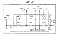
- the floating switch unit 7 comprises six switch portions SW1H, SW1L, SW2H, SW2L, SW3H, and SW3L, and the different point from FIG. 5 of the above-described embodiment is the relation of the connection of the switch portions SW2H and SW2L and the switch portions SW3H and SW3L.
- the one connecting part of the switch portion SW4H is connected to the other connecting part of the switch SW1H, and the one connecting part of the switch portion SW4L is connected to the other connecting part of the switch SW1L.
- the one connecting part of the switch SW2H is connected to the other connecting part of the switch portion SW4H, and the one connecting part of the switch SW2L is connected to the other connecting part of the switch portion SW4L.
- bus terminals B1 and B2 are connected to the other connecting parts of the switches SW2H and SW2L, respectively. Also the other connecting parts of the switch portions SW3H and SW3L are connected so that the power supply voltage is provided to the floating control circuit 4, the transmitter circuit 5, and the receiver circuit 6, respectively as the floating power supply.
- the capacitance terminals CS1 and CS2 are connected to the other connecting parts of the switch portions SW1H and SW1L, respectively. And the capacitance terminals CH1 and CH2 are connected to the other connecting parts of the switch portions SW3H and SW3L, respectively.
- the electrostatic capacitance element CS is connected externally to the capacitance terminals CS1 and CS2, and the electrostatic capacitance element CH is connected externally to the capacitance terminals CH1 and CH2.
- the switch portions SW1H and SW1L are turned OFF, and the switch portions SW2H, SW3H, SW2L, and SW3L are turned ON, respectively.
- the floating power supply is provided from the electrostatic capacitance element CS to the buses A and B, the floating control circuit 4, the transmitter circuit 5, and the receiver circuit 6.
- the floating switch unit 7 in which the number of the switch portions is considerably reduced can be configured. Also, in the data phase period, since only the switch portions SW3H and SW3L are required to be turned ON, the ON-resistance of each of the switch portions can be increased, whereby the switch units can be downsized.
- the performance can be improved as downsizing the semiconductor integrated circuit device 1. Also, the reliability of the semiconductor integrated circuit device 1 can be improved.
- the present invention is, in a semiconductor integrated circuit device, appropriate for the technique that considerably reduces the number of switches in a switching circuit which provides a floating power supply.
Landscapes
- Engineering & Computer Science (AREA)
- Power Engineering (AREA)
- Electronic Switches (AREA)
- Semiconductor Integrated Circuits (AREA)
Abstract
Description
- The present invention relates to a technique for providing a power supply by a switching circuit, and particularly to a technique effectively applied to provide a power supply of a floating power supply by a switching circuit.
- As an object of establishing a LAN (Local Area Network) of an airbag system in an automobile, LAN protocols established by Safe-by-Wire Plus consortium and ISO (International Organization for Standardization)/IEC (International Electrotechnical Commission) are known (see Non-Patent
Document 1 and Non-Patent Document 2). - The above-described standards define common specifications for an airbag control unit, a communication protocol between controllers which controls a peripheral device such as an airbag and a seatbelt, and a driver unit which drives a bus, and the requisite minimum specifications are determined.
- And, the airbag control unit serving as a controller which controls the bus is called a "master", and a side of controlling the peripheral device such as an airbag and a seatbelt is called a "slave". The bus connects two lines of the master and the slave and becomes a path for providing the power supply and an operation of a bidirectional communication from a bus interface of the master side to a bus interface of the slave.
- In the airbag control unit, a floating switch unit is used in the bus interface so that communication can be continued even when one side of the buses is short-circuited to a battery (power supply voltage) or a ground potential (reference potential).
- For example, when the bus A is short-circuited to the battery, the voltage level of the bus B is shifted to the battery voltage side, and when the bus B is short-circuited to the ground potential, the voltage level of the bus A is shifted to the ground potential side, whereby the configuration is operated so that a voltage differential between the buses (the bus A - the bus B) is always maintained.
- And, the floating switch unit comprises, for example, a switch which charges a first electrostatic capacitance from a battery power supply, a switch which provides the power supply from the first electrostatic capacitance to a transmitter circuit and the like, a switch which provides the power supply from the first electrostatic capacitance to the bus, a switch which charges a second electrostatic capacitance from the battery power supply, a switch which provides the power supply from the second electrostatic capacitance to a bus driver, and others.
- Non-Patent Document 1: Automotive Safety Restraints BUS (ASRB) 2.0
- Non-Patent Document 2: ISO/IEC 22896: Road Vehicles-Deployment and sensor bus for passenger safety systems
- However, in the switching technique by the floating switch unit in the airbag control unit described above, the present inventors have found the following problems.
- That is, since the above-described floating switch unit is required a MOS (Metal Oxide Semiconductor) transistor with high breakdown voltage, an element area of the transistor configuring the switch is comparatively large.
- By this manner, downsizing of a semiconductor integrated circuit device configuring the airbag control unit is difficult, therefore there is also a problem that the manufacturing cost is high.
- And, the required current value is different depending on the number or the type of the slave connected to the bus. However, the current has to be increased in order to enable a plurality of connection, therefore, it can be easily expected that the chip area occupied by a transistor element is further increased in order to decrease the ON-resistance of the switch.
- An object of the present invention is to provide a technique which considerably reduces the number of switches in a switching circuit which provides a floating power supply and achieves downsizing and low-cost of a semiconductor integrated circuit device.
- The above and other objects and novel characteristics of the present invention will be apparent from the description of this specification and the accompanying drawings.
- The typical ones of the inventions disclosed in this application will be briefly described as follows.
- The present invention includes a semiconductor integrated circuit device having two externally-connected buses and a switching circuit providing the power supply voltage to an arbitrary internal peripheral circuit, wherein the switching circuit comprises: a first switch unit connecting, to an externally-connected a first electrostatic capacitance element, the power supply voltage provided from the battery; a second switch unit providing a electrostatic capacitance charged in a second electrostatic capacitance element to the bus; and a third switch unit charging the electrostatic capacitance in the first electrostatic capacitance element to the second electrostatic capacitance element and providing the power supply to the internal peripheral circuit.
- Also, a summary of other invention of the present application will be briefly described.
- The present invention comprises in which the first switch unit comprising a first Hi-side switch portion in which a one connecting part thereof is connected to the battery power supply side and the other connecting part thereof is connected to a one connecting part of the first electrostatic capacitance element and comprising a first Lo-side switch portion in which a one connecting part thereof is connected to the battery reference potential side and the other connecting part thereof is connected to the other connecting part of the first electrostatic capacitance element, the second switch unit comprising a second Hi-side switch portion in which a one connecting part thereof is connected to a one connecting part of the first electrostatic capacitance element and the other connecting part thereof is connected to one of the buses and comprising a second Lo-side switch portion in which a one connecting part thereof is connected to the other connecting part of the first electrostatic capacitance element and the other connecting part thereof is connected to the other of the buses, and the third switch unit comprising a third Hi-side switch portion in which a one connecting part thereof is connected to a one connecting part of the first electrostatic capacitance element and the other connecting part thereof is connected to a one connecting part of the second electrostatic capacitance element and comprising a third Lo-side switch portion in which a one connecting part thereof is connected to the other connecting part of the first electrostatic capacitance element and the other connecting part thereof is connected to the other connecting part of the second electrostatic capacitance element.
- Also, the present invention comprises the first switch unit comprising the first Hi-side switch portion in which a one connecting part thereof is connected to the battery power supply side and the other connecting part thereof is connected to a one junction part of the first electrostatic capacitance element and comprising the first Lo-side switch portion in which a one connecting part thereof is connected to the battery reference potential side and the other connecting part thereof is connected to the other connecting part of the first electrostatic capacitance element, the third switch unit comprising the third Hi-side switch portion in which a one connecting part thereof is connected to a one connecting part of the first electrostatic capacitance element and the other connecting part thereof is connected to a one connecting part of the second electrostatic capacitance element and comprising the third Lo-side switch portion in which a one connecting part thereof is connected to the other connecting part of the first electrostatic capacitance element and the other connecting part thereof is connected to the other connecting part of the second electrostatic capacitance element, and the second switch unit comprising the second Hi-side switch portion in which a one connecting part thereof is connected to a one connecting part of the second electrostatic capacitance element and the other connecting part thereof is connected to one of the buses and comprising the second Lo-side switch portion in which a one connecting part thereof is connected to the other connecting part of the second electrostatic capacitance element and the other connecting part thereof is connected to the other of the buses.
- Besides, the present invention comprises each of the first to third Hi-side switch portions comprising first and second transistors connected in series and comprising a P-channel MOS operating as a switch and comprising a first gate control unit generating a gate control signal from an inputted control signal and driving and controlling the first transistor by the gate control signal and comprising a second gate control unit outputting the gate control signal from an inputted control signal and driving and controlling the second transistor by the gate control signal and comprising a first power supply generating unit generating a power supply voltage by which the first gate control unit is operated and comprising a second power supply generating unit generating a power supply voltage by which the second gate control unit is operated, and each of the first to third Lo-side switch portions comprising third and fourth MOS transistors connected in series and operating as a switch and comprising a third gate control unit generating a gate control signal from an inputted control signal and driving and controlling the third transistor by the gate control signal and comprising a fourth gate control unit generating a gate control signal from an inputted control signal and driving and controlling the fourth transistor by the gate control signal and comprising a third power supply generating unit generating a power supply voltage by which the third gate control unit is operated and comprising a fourth power supply generating unit generating a power supply voltage by which the fourth gate control unit is operated.
- Also, the present invention comprises the first to fourth gate control units comprising level shift units which level-shift the inputted control signals, to convert them to voltage levels for driving the first to fourth transistors, and output them and driver units which generate the gate control signals driving the first to fourth transistors from the signals outputted from the level shift units, and output them.
- Moreover, the present invention comprises the driver units each has a configuration in which two invertors are connected in series.
- Further, the present invention comprises in which the first to fourth power supply generating units are provided with Zener diodes connected between the power supply voltages provided from the battery, and the power supply voltages which generate, as references, Zener voltages of the Zener diodes are provided to the first to fourth gate control units.
- Still further, the present invention comprises in which the first to fourth power supply generating units are provided with: first Zener diodes whose cathodes are connected to the power supply side of the battery; second Zener diodes whose cathodes are connected to anodes of the first Zener diodes and anodes are connected to the reference potential side of the battery; and switches connected between the anodes and the cathodes of the second Zener diodes; and the switches become non-conductive states in performing acceleration tests of gate breakdown voltages in the first to fourth transistors.
- Effects obtained by typical ones of the inventions disclosed in the present application will be briefly described below.
- (1) The semiconductor integrated circuit device can be downsized.
- (2) Reliability of the semiconductor integrated circuit device can be increased.
-
-
FIG. 1 is a block diagram showing a configuration example of a semiconductor integrated circuit device according to a first embodiment of the present invention; -
FIG. 2 is a timing chart showing a schematic operation of a bus in the semiconductor integrated circuit device ofFIG. 1 ; -
FIG. 3 is a timing chart showing a schematic operation of a case in which the bus in the semiconductor integrated circuit device ofFIG. 1 is short-circuited to a battery; -
FIG. 4 is a timing chart showing a schematic operation of a case in which the bus in the semiconductor integrated circuit device ofFIG. 1 is short-circuited to a ground potential; -
FIG. 5 is an explanatory diagram showing a configuration example of a floating switch unit provided in the semiconductor integrated circuit device ofFIG. 1 ; -
FIG. 6 is an explanatory diagram showing a configuration example of a switch unit provided in the semiconductor integrated circuit device ofFIG. 1 ; -
FIG. 7 is an explanatory diagram showing a configuration example of a voltage generating unit and a gate control unit provided in the switch unit ofFIG. 6 ; -
FIG. 8 is an explanatory diagram showing another configuration example of the voltage generating unit and the gate control unit provided in the switch unit ofFIG. 6 ; -
FIG. 9 is an explanatory diagram showing a configuration example of a voltage generating unit and a gate control unit provided in a switch unit according to another embodiment of the present invention; and -
FIG. 10 is an explanatory diagram showing a configuration example of a floating switch unit according to a second embodiment of the present invention. - Hereinafter, embodiments of the present invention will be described in detail with reference to the accompanying drawings. Note that components having the same function are denoted by the same reference symbols throughout the drawings for describing the embodiment, and the repetitive description thereof will be omitted.
- According to the present embodiment, a semiconductor integrated
circuit device 1 is used for an airbag system of an automobile and is used as a communication device which controls a bus in the LAN protocol of Automotive Safety Restraints BUS (ASRB) 2.0. - As shown in
FIG. 1 , the semiconductorintegrated circuit device 1 comprises acontrol unit 2, alevel shift 3, afloating control circuit 4, atransmitter circuit 5, areceiver circuit 6, and afloating switch unit 7. - Two buses A and B are connected to the
transmitter circuit 5, thereceiver circuit 6, and thefloating switch unit 7. A slave unit SU which controls a peripheral device such as an airbag and a seatbelt is connected to the buses A and B. - And, to the
floating control circuit 4, thetransmitter circuit 5, and thereceiver circuit 6 which are an internal peripheral circuit, the floating power supply is connected so as to be provided from thefloating switch unit 7. - An MCU (Micro Controller Unit) which controls the entire airbag system through a control terminal is connected to the
control unit 2. And a power supply voltage provided from an automobile battery BAT or the like is connected to thecontrol unit 2, thelevel shift 3, and thefloating switch unit 7 so as to be provided. Electrostatic capacitance elements CS and CH are connected externally to thefloating switch unit 7, respectively. - The
control unit 2 performs all control of the semiconductorintegrated circuit device 1. Thelevel shift 3 is an interface which performs a level conversion of a signal transmitted and received between thefloating control circuit 4 operated by the floating power supply and thecontrol unit 2 operated by the power supply voltage provided from the automobile battery BAT or the like. - The
floating control circuit 4 performs a switching control of thefloating switch unit 7 and controls a transmission/reception signal inputted from and outputted to the buses A and B through thetransmitter circuit 5 and thereceiver circuit 6. - The
transmitter circuit 5 controls the voltage between the buses A and B, and thereceiver circuit 6 determines the voltage level between the buses A and B. Thefloating switch unit 7 charges the electrostatic capacitance elements CS and CH by power supply provided from the battery BAT, provides power supply to the buses A and B and at the same time provides power supply to thefloating control circuit 4, thetransmitter circuit 5, and thereceiver circuit 6 which operate as the floating circuit. - Schematic operation outlines of the buses A and B will be described by using
FIG. 2 to FIG. 4 . - The plurality of slave units SU on a slave side are connected to the buses A and B as described above, and communication is established through the buses A and B. In operations of the buses, as shown in
FIG. 2 , a power phase (Tx=Lo) and a data phase (Tx=Hi) are alternately switched. - The power phase is used for providing power supply from the master to the slave, and the data phase is used for transmission/reception of data. In the transmission/reception of data, the data is determined by a voltage level difference between the buses A and B (bus A - bus B) of the two lines.
- For example, when the voltage level difference is at a voltage VP or more, it is regarded as the power phase, and when being at a lower voltage level than that, it is regarded as the data phase. In the data phase, '0' is determined at a voltage V0, and '1' is determined at a voltage V1 which is lower than the voltage V0.
- And, a level at a voltage V1S0 which is lower than the voltage V1 is a special level and is used, for example, for ordering ignition of an airbag and the like.
- The bus interface part, which comprises the floating
control unit 4, thetransmitter circuit 5, thereceiver circuit 6 and the like, becomes a floating circuit so that communication can be continued even when either one of the buses A and B is short-circuited to the power supply side of the battery BAT or a ground potential GND serving as a reference potential. For example, when the bus A is short-circuited to the battery, as shown inFIG. 3 , the voltage level of the bus B is shifted to the battery voltage side and as shown inFIG. 4 , when the bus B is short-circuited to the ground potential GND, the voltage level of the bus A is shifted to the ground potential GND side, whereby the buses operate so that a voltage difference of the buses (BUS A - BUS B) is always maintained. -
FIG. 5 is an explanatory diagram showing a configuration example of the floatingswitch unit 7. InFIG. 5 , "CL" represents a bus load capacitance, and "ZL" represents a bus load impedance. - As shown in Figure, the floating
switch unit 7 comprises: switch portions SW1H and SW1L configuring a first switch unit; switch portions SW2H and SW2L configuring a second switch unit; and switch portions SW3H and SW3L configuring a third switch unit. - The switch portion SW1H as a first Hi-side switch unit and the switch portion SW1L as a first Lo-side switch unit function as a switch for performing charges from the battery BAT to the electrostatic capacitance element CS.
- The switch portion SW2H as a second Hi-side switch unit and the switch portion SW2L as a second Lo-side switch unit function as a switch for performing charges from the electrostatic capacitance element CS as a first electrostatic capacitance element to the electrostatic capacitance element CH as a second electrostatic capacitance element.
- The switch portion SW3H as a third Hi-side switch unit and the switch portion SW3L as a third Lo-side switch unit function as a switch which connects the electrostatic capacitance element CS to each of the buses A and B.
- A one connecting part of the switch portion SW1H is connected to a power supply terminal VBAT, and a one connecting part of the switch portion SW1L is connected to a ground potential terminal GD. And the battery BAT is connected externally through the power supply terminal VBAT and the ground potential terminal GD.
- The other connecting part of the switch portion SW1H is connected to a one connecting part of the switch portion SW2H, SW3L and a capacitance terminal CS1, respectively. The other connecting part of the switch portion SW1L is connected to a one connecting part of the switch portion SW2L, SW3H and a capacitance terminal CS2, respectively. The electrostatic capacitance element CS is connected externally to the capacitance terminals CS1 and CS2.
- A bus terminal B1 is connected to the other connecting part of the switch portion SW2H, and a bus terminal B2 is connected to the other connecting part of the switch portion SW2L, and the buses A and B are connected to the bus terminals B1 and B2, respectively.
- The capacitance terminal CS1 is connected to the other connecting part of the switch portion SW3H, and the capacitance terminal CS2 is connected to the other connecting part of the switch portion SW3L. The electrostatic capacitance element CH is connected externally to the capacitance terminals CS1 and CS2.
- Also, the other connecting parts of the switch portions SW3H and SW3L are connected respectively so that the power supply voltage is provided as a floating power supply to the floating
control circuit 4, thetransmitter circuit 5, and thereceiver circuit 6. - Next, an operation of the floating
switch unit 7 according to the present embodiment will be described. - First, during a normal operation, as described above, the power phase and the data phase are repeated. In a power phase period, the switch portions SW2H and SW2L and the switch portions SW3H and SW3L are turned ON (conductive state) respectively, and the switch portions SW1H and SW1L are turned OFF (non-conductive state), and the floating power supply is provided from the electrostatic capacitance element CS to each of the buses A and B, the floating
control circuit 4, thetransmitter circuit 5, and thereceiver circuit 6. - In a data phase period, the switch portions SW1H and SW1L are turned ON, and the switch portions SW2H, SW2L, SW3H, and SW3L are turned OFF. Thereby, the electrostatic capacitance element CS is charged by the power supply of the battery BAT, and the electrostatic capacitance element CH provides the floating power supply to each of the floating
control circuit 4, thetransmitter circuit 5, and thereceiver circuit 6. - And, when the power supply is turned on, since the electrostatic capacitance elements CH and CS are not charged, only providing the power supply is repeated until a voltage level is increased by a certain level. In this case, in a period corresponding to the data phase, only the switch portions SW1H and SW1L are turned ON, whereby the electrostatic capacitance element CS is charged from the power supply of the battery BAT, and the electrostatic capacitance element CH provides the power supply voltage to each of the floating
control circuit 4, thetransmitter circuit 5, and thereceiver circuit 6. - In a period corresponding to the power phase, the switch portions SW3H and SW3L are turned ON, thereby performing charges from the electrostatic capacitance element CS to the electrostatic capacitance element CH and at the same time providing the power supply voltage to each of the floating
control circuit 4, thetransmitter circuit 5, and thereceiver circuit 6. And, when the power supply is turned ON, since providing the power supply is not performed to the buses A and B, the switch portions SW3H and SW3L are turned OFF. - By this manner, the floating
switch unit 7 in which the number of switch portions is significantly reduced can be configured. In the data phase period, since only the switch portions SW3H and SW3L are turned ON, ON-resistance of each of the switch portions can be increased, whereby the switch portions can be downsized. - Next, configuration examples of the switch portions SW1H and SW1L will be described by using
FIG. 6 to FIG. 8 . - As shown in
FIG. 6 , the switch portion SW1H comprises:voltage generating units gate control units transistors - The switch portion SW1L comprises:
voltage generating units gate control units transistors - The
voltage generating units gate control units voltage generating units gate control units - The
voltage generating units gate control units voltage generating units gate control units - The
gate control units control unit 4, the gate control signal, which drives thetransistors transistors transistors FIG. 5 . Thegate control units control unit 4, the gate control signal, which drives thetransistors transistors transistors FIG. 5 . - In
FIG. 6 , the configuration example of the switch portion SW1H and the switch portion SW1L has been shown. However, the configurations of the switch portion SW2H, SW3H, SW2L, and SW3L are also similar to configurations shown byFIG. 6 . -
FIG. 7 is an explanatory diagram showing a configuration example of thevoltage generating unit 7 and thegate control unit 9 in the switch portion SW1H. - As shown in Figure, the
voltage generation unit 8 comprises aZener diode 20 and P-type transistors 21 and 22 composed of bipolars, and thegate control unit 10 comprises alevel shifter 23 andinverters 24 and 25. - A cathode of the
Zener diode 20 is connected to the NODE a, and an anode of theZener diode 20 is connected to the NODE b. The anode of theZener diode 20 is connected to a base of thetransistor 22. - And, a base of the transistor 21 is connected to an emitter of the
transistor 22. Each collector of thetransistors 21 and 22 is connected to the NODE b. An emitter of the transistor 21 is connected to the NODE b'. - To an input part of the
level shifter 23, a control signal outputted from the floatingcontrol unit 4 is connected so as to be inputted. And to an output part of thelevel shifter 23, theinverters 24 and 25 are configured to be connected in series. - To power supply parts of the
level shifter 23 and theinverters 24 and 25, the voltage level between the NODE a and the NODE b', that is, such a power supply voltage that a Zener voltage of theZener diode 20 is generated as a reference is connected. - Therefore, the control signal outputted from the floating
control unit 4 is converted in voltage level by thelevel shifter 23, and then, through theinverters 24 and 25, is outputted as a gate control signal which drives thetransistor 12. - In this manner, by using the
inverters 24 and 25 in driving thetransistor 12, thetransistor 12 can be driven at high speed. And, by using theinverters 24 and 25, power consumption can be reduced, whereby power consumption reduction of the semiconductor integratedcircuit device 1 can be realized. -
FIG. 8 is an explanatory diagram showing a configuration example of thevoltage generating unit 14 and thegate control unit 16 in the switch portion SW1L. - As shown in the diagram, the
voltage generating unit 14 comprises: aZener diode 26; and N-type transistors gate control unit 16 comprises alevel shifter 29 andinverters - A cathode of the
Zener diode 26 is connected to the NODE a, and an anode of theZener diode 26 is connected to the NODE b. A cathode of theZener diode 26 is connected to a base of thetransistor 27. - Each collector of the
transistors transistor 27 is connected to a base of thetransistor 28. And an emitter of thetransistor 28 is connected to the NODE a'. - Also, to an input part of the
level shifter 29, the control signal outputted from the floatingcontrol unit 4 is connected so as to be inputted. And to an output part of thelevel shifter 29, theinverters - To power supply parts of the
level shifter 29 and theinverters Zener diode 26 is generated as a reference is connected. - Also in this case, the control signal output from the floating
control unit 4 is converted the voltage level by thelevel shifter 29, and then, through theinverters transistor 17. - And, in
FIG. 7 andFIG. 8 , the configuration examples of thevoltage generating units gate control units voltage generating units gate control units - In this manner, by the configuration of driving the
transistors inverters transistors - By this manner according to the first embodiment, the performance can be improved as downsizing the semiconductor integrated
circuit device 1. Besides, the reliability of the semiconductor integratedcircuit device 1 can be improved. - Also, for example, the
voltage generating unit 13 can be configured enable to easily perform an acceleration test of a gate breakdown voltage in the MOS transistor which functions as a transistor for switching. - In this case, as shown in
FIG. 9 , in thevoltage generating unit 13, a Zener diode 26a which functions as a new first Zener diode is connected in series to aZener diode 26 which functions as a first Zener diode, and a switch 32 is provided between the anode and the cathode of the Zener diode 26a. - Normally, the switch 32 is turned ON. By turning it OFF when performing an acceleration test of a gate breakdown voltage in the
transistor 18, the voltage applied to the gate of thetransistor 18 can be easily increased. Note that, herein, although thevoltage generating unit 14 has been described, it is configured so that the similar circuit is added to all of the voltage generating units. - In a second embodiment, the semiconductor integrated
circuit device 1 comprises, as same with the above-described first embodiment (FIG. 1 ), thecontrol unit 2, thelevel shift 3, the floatingcontrol circuit 4, thetransmitter circuit 5, thereceiver circuit 6, and the floatingswitch unit 7. - And, as shown in
FIG. 10 , the floatingswitch unit 7 comprises six switch portions SW1H, SW1L, SW2H, SW2L, SW3H, and SW3L, and the different point fromFIG. 5 of the above-described embodiment is the relation of the connection of the switch portions SW2H and SW2L and the switch portions SW3H and SW3L. - In this case, the one connecting part of the switch portion SW4H is connected to the other connecting part of the switch SW1H, and the one connecting part of the switch portion SW4L is connected to the other connecting part of the switch SW1L.
- Also, the one connecting part of the switch SW2H is connected to the other connecting part of the switch portion SW4H, and the one connecting part of the switch SW2L is connected to the other connecting part of the switch portion SW4L.
- And, bus terminals B1 and B2 are connected to the other connecting parts of the switches SW2H and SW2L, respectively. Also the other connecting parts of the switch portions SW3H and SW3L are connected so that the power supply voltage is provided to the floating
control circuit 4, thetransmitter circuit 5, and thereceiver circuit 6, respectively as the floating power supply. - The capacitance terminals CS1 and CS2 are connected to the other connecting parts of the switch portions SW1H and SW1L, respectively. And the capacitance terminals CH1 and CH2 are connected to the other connecting parts of the switch portions SW3H and SW3L, respectively. The electrostatic capacitance element CS is connected externally to the capacitance terminals CS1 and CS2, and the electrostatic capacitance element CH is connected externally to the capacitance terminals CH1 and CH2.
- In the floating
switch unit 7 according to the second embodiment, in the power phase period when in normal operation, the switch portions SW1H and SW1L are turned OFF, and the switch portions SW2H, SW3H, SW2L, and SW3L are turned ON, respectively. Through the switch portions SW2H, SW3H, SW2L and SW3L, the floating power supply is provided from the electrostatic capacitance element CS to the buses A and B, the floatingcontrol circuit 4, thetransmitter circuit 5, and thereceiver circuit 6. - Also, about the other operations, the explanation thereof is omitted since they are similar to those of the above-described first embodiment.
- Therefore, also in this case, the floating
switch unit 7 in which the number of the switch portions is considerably reduced can be configured. Also, in the data phase period, since only the switch portions SW3H and SW3L are required to be turned ON, the ON-resistance of each of the switch portions can be increased, whereby the switch units can be downsized. - By this manner, also in the second embodiment, the performance can be improved as downsizing the semiconductor integrated
circuit device 1. Also, the reliability of the semiconductor integratedcircuit device 1 can be improved. - In the foregoing, the invention made by the inventors of the present invention has been concretely described based on the embodiments. However, it is needless to say that the present invention is not limited to the foregoing embodiments and various modifications and alterations can be made within the scope of the present invention.
- The present invention is, in a semiconductor integrated circuit device, appropriate for the technique that considerably reduces the number of switches in a switching circuit which provides a floating power supply.
Claims (8)
- A semiconductor integrated circuit device having two externally-connected buses and a switching circuit which provides a power supply voltage to an arbitrary internal peripheral circuit, wherein
the switching circuit comprises:a first switch unit connecting, to an externally-connected first electrostatic capacitance element, the power supply voltage provided from a battery;a second switch unit providing an electrostatic capacitance charged in a second electrostatic capacitance element to the buses; anda third switch unit charging an electrostatic capacitance of the first electrostatic capacitance element to the second electrostatic capacitance element and providing power supply to the internal peripheral circuit. - The semiconductor integrated circuit device according to claim 1, wherein
the first switch unit comprises:a first Hi-side switch portion in which a one connecting part thereof is connected to a power supply side of the battery and the other connecting part thereof is connected to a one connecting part of the first electrostatic capacitance element; anda first Lo-side switch portion in which a one connecting part thereof is connected to a reference potential side of the battery and the other connecting part thereof is connected to the other connecting part of the first electrostatic capacitance element,the second switch unit comprises:a second Hi-side switch portion in which a one connecting part thereof is connected to a one connecting part of the first electrostatic capacitance element and the other connecting part thereof is connected to one of the buses; anda second Lo-side switch portion in which a one connecting part thereof is connected to the other connecting part of the first electrostatic capacitance element and the other connecting part thereof is connected to the other of the buses, andthe third switch unit comprises:a third Hi-side switch portion in which a one connecting part thereof is connected to a one connecting part of the first electrostatic capacitance element and the other connecting part thereof is connected to a one connecting part of the second electrostatic capacitance element; anda third Lo-side switch portion in which a one connecting part thereof is connected to the other connecting part of the first electrostatic capacitance element and the other connecting part thereof is connected to the other connecting part of the second electrostatic capacitance element. - The semiconductor integrated circuit device according to claim 1, wherein
the first switch unit comprises:a first Hi-side switch portion in which a one connecting part thereof is connected to a power supply side of the battery and the other connecting part thereof is connected to a one connecting part of the first electrostatic capacitance element; anda first Lo-side switch portion in which a one connecting part thereof is connected to a reference potential side of the battery and the other connecting part thereof is connected to the other connecting part of the first electrostatic capacitance element,the third switch unit comprises:a third Hi-side switch portion in which a one connecting part thereof is connected to a one connecting part of the first electrostatic capacitance element and the other connecting part thereof is connected to a one connecting part of the second electrostatic capacitance element; anda third Lo-side switch portion in which a one connecting part thereof is connected to the other connecting part of the first electrostatic capacitance element and the other connecting part thereof is connected to the other connecting part of the second electrostatic capacitance element, andthe second switch part comprises:a second Hi-side switch portion in which a one connecting part thereof is connected to a one connecting part of the second electrostatic capacitance element and the other connecting part thereof is connected to one of the buses; anda second Lo-side switch portion in which a one connecting part thereof is connected to the other connecting part of the second electrostatic capacitance element and the other connecting part thereof is connected to the other of the buses. - The semiconductor integrated circuit device according to claim 2 or 3, wherein
each of the first to third Hi-side switch portions comprises:
first and second MOS transistors which are connected in series and operated as a switch;
a first gate control unit which generates a gate control signal from an inputted control signal and drives and controls the first MOS transistor by the gate control signal;
a second gate control unit which outputs a gate control signal from an inputted control signal and drives and controls the second MOS transistor by the gate control signal;
a first power supply generating unit which generates a power supply voltage by which the first gate control unit is operated; and
a second power supply generating unit which generates a power supply voltage by which the second gate control unit is operated, and
each of the first to third Lo-side switch portions comprises:
third and fourth MOS transistors which are connected in series and operated as a switch;
a third gate control unit which generates a gate control signal from an inputted control signal and drives and controls the third MOS transistor by the gate control signal;
a fourth gate control unit which generates a gate control signal from an inputted control signal and drives and controls the fourth transistor by the gate control signal;
a third power supply generating unit which generates a power supply voltage by which the third gate control unit is operated; and
a fourth power supply generating unit which generates a power supply voltage by which the fourth gate control unit is operated. - The semiconductor integrated circuit device according to claim 4, wherein
the first to fourth gate control units comprise:level shift units which level-shift the inputted control signals, to convert them to voltage levels for driving the first to fourth MOS transistors, and output them; anddriver units which generate the gate control signals driving the first to fourth MOS transistors from the signals outputted from the level shift units, and output them. - The semiconductor integrated circuit device according to claim 5, wherein
the driver units each have a configuration in which two inverters are connected in series. - The semiconductor integrated circuit device according to any one of claims 4 to 6, wherein
the first to fourth power supply generating units comprise Zener diodes connected between the power supply voltages provided from the battery, and
power supply voltages which generate, as references, Zener voltages of the Zener diodes are provided to the first to fourth gate control units. - The semiconductor integrated circuit device according to any one of claims 4 to 6, wherein
the first to fourth power supply generating units comprise:
first Zener diodes whose cathodes are connected to the power supply side of the battery;
second Zener diodes whose cathodes are connected to anodes of the first Zener diodes and whose anodes are connected to the reference potential side of the battery; and
switches connected between the anodes and the cathodes of the second Zener diodes, and
the switches become non-conductive states in performing acceleration tests of gate breakdown voltages in the first to fourth MOS transistors.
Applications Claiming Priority (1)
| Application Number | Priority Date | Filing Date | Title |
|---|---|---|---|
| PCT/JP2006/313126 WO2008001467A1 (en) | 2006-06-30 | 2006-06-30 | Semiconductor integrated circuit device |
Publications (3)
| Publication Number | Publication Date |
|---|---|
| EP2040378A1 true EP2040378A1 (en) | 2009-03-25 |
| EP2040378A4 EP2040378A4 (en) | 2011-02-23 |
| EP2040378B1 EP2040378B1 (en) | 2012-09-19 |
Family
ID=38845242
Family Applications (1)
| Application Number | Title | Priority Date | Filing Date |
|---|---|---|---|
| EP20060780693 Not-in-force EP2040378B1 (en) | 2006-06-30 | 2006-06-30 | Semiconductor integrated circuit device |
Country Status (5)
| Country | Link |
|---|---|
| US (2) | US7989988B2 (en) |
| EP (1) | EP2040378B1 (en) |
| JP (1) | JP4977701B2 (en) |
| CN (1) | CN101473538B (en) |
| WO (1) | WO2008001467A1 (en) |
Families Citing this family (12)
| Publication number | Priority date | Publication date | Assignee | Title |
|---|---|---|---|---|
| JP5378930B2 (en) | 2009-09-28 | 2013-12-25 | ルネサスエレクトロニクス株式会社 | Semiconductor device and wireless communication device |
| US9112494B2 (en) | 2011-07-28 | 2015-08-18 | Infineon Technologies Ag | Charge pump driven electronic switch with rapid turn off |
| US8723491B2 (en) | 2011-12-19 | 2014-05-13 | Arctic Sand Technologies, Inc. | Control of power converters with capacitive energy transfer |
| CN104782040A (en) * | 2012-08-17 | 2015-07-15 | 先端充电技术公司 | Power device |
| US9520799B2 (en) | 2012-08-17 | 2016-12-13 | Advanced Charging Technologies, LLC | Power device |
| US9991821B2 (en) | 2012-08-17 | 2018-06-05 | Advanced Charging Technologies, LLC | Transformerless multiple output capable power supply system |
| US9203299B2 (en) | 2013-03-15 | 2015-12-01 | Artic Sand Technologies, Inc. | Controller-driven reconfiguration of switched-capacitor power converter |
| US8619445B1 (en) | 2013-03-15 | 2013-12-31 | Arctic Sand Technologies, Inc. | Protection of switched capacitor power converter |
| US8724353B1 (en) | 2013-03-15 | 2014-05-13 | Arctic Sand Technologies, Inc. | Efficient gate drivers for switched capacitor converters |
| DE102016111036B4 (en) * | 2016-06-16 | 2017-12-28 | Infineon Technologies Ag | Circuit and method of operating the circuit |
| US10505444B1 (en) * | 2018-10-04 | 2019-12-10 | Xilinx, Inc. | Voltage divider and method of implementing a voltage divider |
| JP7251351B2 (en) * | 2019-06-24 | 2023-04-04 | 富士電機株式会社 | Gate drive and power converter |
Family Cites Families (9)
| Publication number | Priority date | Publication date | Assignee | Title |
|---|---|---|---|---|
| JPS5280423A (en) * | 1975-12-26 | 1977-07-06 | M Syst Giken Kk | Dccdc converter |
| US4807104A (en) | 1988-04-15 | 1989-02-21 | Motorola, Inc. | Voltage multiplying and inverting charge pump |
| CN2138595Y (en) * | 1992-08-03 | 1993-07-21 | 何顺禄 | Safety air bag for vehicle driver |
| JPH08332913A (en) * | 1995-04-07 | 1996-12-17 | Kansei Corp | Occupant crash protection for vehicle |
| CN2335840Y (en) * | 1998-12-28 | 1999-09-01 | 张根发 | Mechanoelectric collision transducer for controlling automotive safety air bag device |
| JP2004140756A (en) * | 2002-10-21 | 2004-05-13 | Renesas Technology Corp | Load controller and power line communication apparatus |
| DE60332383D1 (en) * | 2002-11-18 | 2010-06-10 | Nxp Bv | INTEGRATED FLOATING POWER TRANSMISSION DEVICE AND CORRESPONDING METHOD |
| JP3595329B1 (en) * | 2003-07-30 | 2004-12-02 | 有限会社オデオ | Power supply insulation circuit |
| JP2005176131A (en) * | 2003-12-12 | 2005-06-30 | Sumitomo Electric Ind Ltd | Communication system in a mobile body |
-
2006
- 2006-06-30 US US12/306,500 patent/US7989988B2/en not_active Expired - Fee Related
- 2006-06-30 EP EP20060780693 patent/EP2040378B1/en not_active Not-in-force
- 2006-06-30 CN CN2006800551351A patent/CN101473538B/en not_active Expired - Fee Related
- 2006-06-30 JP JP2008522270A patent/JP4977701B2/en not_active Expired - Fee Related
- 2006-06-30 WO PCT/JP2006/313126 patent/WO2008001467A1/en not_active Ceased
-
2011
- 2011-07-08 US US13/178,933 patent/US8093762B2/en active Active
Also Published As
| Publication number | Publication date |
|---|---|
| JP4977701B2 (en) | 2012-07-18 |
| CN101473538A (en) | 2009-07-01 |
| US20110260776A1 (en) | 2011-10-27 |
| US20090200874A1 (en) | 2009-08-13 |
| CN101473538B (en) | 2011-12-07 |
| EP2040378B1 (en) | 2012-09-19 |
| US8093762B2 (en) | 2012-01-10 |
| WO2008001467A1 (en) | 2008-01-03 |
| EP2040378A4 (en) | 2011-02-23 |
| US7989988B2 (en) | 2011-08-02 |
| JPWO2008001467A1 (en) | 2009-11-26 |
Similar Documents
| Publication | Publication Date | Title |
|---|---|---|
| US8093762B2 (en) | Semiconductor integrated circuit device | |
| US8836300B2 (en) | Step-down switching regulator | |
| EP2624455B1 (en) | Level shift circuit | |
| JP4148162B2 (en) | Circuit system | |
| CN102290982A (en) | Transmitter, interface device, and car mounted communication system | |
| US20100253392A1 (en) | I/o buffer with twice the supply voltage tolerance using normal supply voltage devices | |
| CN111342541B (en) | Power supply switching circuit | |
| CN102904554B (en) | Drive electronic switch | |
| CN103227656B (en) | Bi-directional transceiver and method | |
| US20090085542A1 (en) | Drive system for power semiconductor device | |
| CN111277247B (en) | A position pulse generating circuit and driving method thereof | |
| US7626441B2 (en) | Drive circuit with BOT level shifter for transmitting an input signal and assigned method | |
| US20050248381A1 (en) | Level shift circuit | |
| US6741116B2 (en) | Semiconductor component for direct gate control and monitoring of power semiconductor switches | |
| CN112585864B (en) | Power module and its level conversion circuit | |
| US20060038544A1 (en) | Power supply circuit capable of rapidly changing output voltages | |
| US20260051883A1 (en) | GATE DRIVER CIRCUIT and CHIP | |
| US11539312B2 (en) | Motor driver and motor driving system | |
| CN113615089B (en) | Switching device for converting a differential input signal and system having a switching device | |
| JP5321000B2 (en) | Level shift circuit | |
| CN101290712A (en) | Output current pumping circuit and remote controller using the same | |
| CN117394723A (en) | Motor pre-driving circuit and motor control system | |
| US20240283269A1 (en) | Switch control device and battery pack including the same | |
| EP4727070A1 (en) | Can transceiver | |
| CN223067028U (en) | Motor driving circuit, chip and system |
Legal Events
| Date | Code | Title | Description |
|---|---|---|---|
| PUAI | Public reference made under article 153(3) epc to a published international application that has entered the european phase |
Free format text: ORIGINAL CODE: 0009012 |
|
| 17P | Request for examination filed |
Effective date: 20090106 |
|
| AK | Designated contracting states |
Kind code of ref document: A1 Designated state(s): AT BE BG CH CY CZ DE DK EE ES FI FR GB GR HU IE IS IT LI LT LU LV MC NL PL PT RO SE SI SK TR |
|
| AX | Request for extension of the european patent |
Extension state: AL BA HR MK RS |
|
| RIN1 | Information on inventor provided before grant (corrected) |
Inventor name: KUBO, KAZUAKI Inventor name: KATO, KIKUO Inventor name: YASHITA, TAKAHIRO Inventor name: TAKAI, KAZUYOSHI |
|
| RBV | Designated contracting states (corrected) |
Designated state(s): DE FR GB IT |
|
| RAP1 | Party data changed (applicant data changed or rights of an application transferred) |
Owner name: RENESAS ELECTRONICS CORPORATION |
|
| A4 | Supplementary search report drawn up and despatched |
Effective date: 20110125 |
|
| RIC1 | Information provided on ipc code assigned before grant |
Ipc: H03K 17/10 20060101ALI20110119BHEP Ipc: H02M 3/07 20060101AFI20110119BHEP |
|
| REG | Reference to a national code |
Ref country code: DE Ref legal event code: R079 Ref document number: 602006032060 Country of ref document: DE Free format text: PREVIOUS MAIN CLASS: H03K0017060000 Ipc: H02M0003070000 |
|
| RIC1 | Information provided on ipc code assigned before grant |
Ipc: H03K 17/10 20060101ALI20120404BHEP Ipc: H02M 3/07 20060101AFI20120404BHEP |
|
| GRAP | Despatch of communication of intention to grant a patent |
Free format text: ORIGINAL CODE: EPIDOSNIGR1 |
|
| DAX | Request for extension of the european patent (deleted) | ||
| GRAS | Grant fee paid |
Free format text: ORIGINAL CODE: EPIDOSNIGR3 |
|
| GRAA | (expected) grant |
Free format text: ORIGINAL CODE: 0009210 |
|
| AK | Designated contracting states |
Kind code of ref document: B1 Designated state(s): DE FR GB IT |
|
| REG | Reference to a national code |
Ref country code: GB Ref legal event code: FG4D |
|
| REG | Reference to a national code |
Ref country code: DE Ref legal event code: R096 Ref document number: 602006032060 Country of ref document: DE Effective date: 20121115 |
|
| PLBE | No opposition filed within time limit |
Free format text: ORIGINAL CODE: 0009261 |
|
| STAA | Information on the status of an ep patent application or granted ep patent |
Free format text: STATUS: NO OPPOSITION FILED WITHIN TIME LIMIT |
|
| PGFP | Annual fee paid to national office [announced via postgrant information from national office to epo] |
Ref country code: GB Payment date: 20130620 Year of fee payment: 8 Ref country code: DE Payment date: 20130626 Year of fee payment: 8 |
|
| 26N | No opposition filed |
Effective date: 20130620 |
|
| REG | Reference to a national code |
Ref country code: DE Ref legal event code: R097 Ref document number: 602006032060 Country of ref document: DE Effective date: 20130620 |
|
| PGFP | Annual fee paid to national office [announced via postgrant information from national office to epo] |
Ref country code: FR Payment date: 20130717 Year of fee payment: 8 |
|
| PGFP | Annual fee paid to national office [announced via postgrant information from national office to epo] |
Ref country code: IT Payment date: 20130628 Year of fee payment: 8 |
|
| REG | Reference to a national code |
Ref country code: DE Ref legal event code: R119 Ref document number: 602006032060 Country of ref document: DE |
|
| GBPC | Gb: european patent ceased through non-payment of renewal fee |
Effective date: 20140630 |
|
| REG | Reference to a national code |
Ref country code: DE Ref legal event code: R119 Ref document number: 602006032060 Country of ref document: DE Effective date: 20150101 |
|
| REG | Reference to a national code |
Ref country code: FR Ref legal event code: ST Effective date: 20150227 |
|
| PG25 | Lapsed in a contracting state [announced via postgrant information from national office to epo] |
Ref country code: DE Free format text: LAPSE BECAUSE OF NON-PAYMENT OF DUE FEES Effective date: 20150101 Ref country code: IT Free format text: LAPSE BECAUSE OF NON-PAYMENT OF DUE FEES Effective date: 20140630 |
|
| PG25 | Lapsed in a contracting state [announced via postgrant information from national office to epo] |
Ref country code: GB Free format text: LAPSE BECAUSE OF NON-PAYMENT OF DUE FEES Effective date: 20140630 Ref country code: FR Free format text: LAPSE BECAUSE OF NON-PAYMENT OF DUE FEES Effective date: 20140630 |