EP2040307A1 - A photodetector for an optical device - Google Patents
A photodetector for an optical device Download PDFInfo
- Publication number
- EP2040307A1 EP2040307A1 EP07301386A EP07301386A EP2040307A1 EP 2040307 A1 EP2040307 A1 EP 2040307A1 EP 07301386 A EP07301386 A EP 07301386A EP 07301386 A EP07301386 A EP 07301386A EP 2040307 A1 EP2040307 A1 EP 2040307A1
- Authority
- EP
- European Patent Office
- Prior art keywords
- photodetector
- transition
- band
- wavelength
- multiplication
- Prior art date
- Legal status (The legal status is an assumption and is not a legal conclusion. Google has not performed a legal analysis and makes no representation as to the accuracy of the status listed.)
- Granted
Links
- 230000003287 optical effect Effects 0.000 title description 5
- 230000007704 transition Effects 0.000 claims abstract description 43
- 238000010521 absorption reaction Methods 0.000 claims abstract description 31
- 239000003574 free electron Substances 0.000 claims abstract description 14
- 238000000034 method Methods 0.000 claims abstract description 11
- 230000004044 response Effects 0.000 claims abstract description 8
- 230000004888 barrier function Effects 0.000 claims description 21
- 239000000969 carrier Substances 0.000 claims description 4
- 230000005641 tunneling Effects 0.000 claims description 4
- 238000010586 diagram Methods 0.000 description 10
- 239000000463 material Substances 0.000 description 10
- 238000000098 azimuthal photoelectron diffraction Methods 0.000 description 6
- 230000005684 electric field Effects 0.000 description 6
- 239000000203 mixture Substances 0.000 description 5
- 239000000243 solution Substances 0.000 description 5
- 229910000661 Mercury cadmium telluride Inorganic materials 0.000 description 3
- 230000005540 biological transmission Effects 0.000 description 3
- 230000000694 effects Effects 0.000 description 3
- 239000004065 semiconductor Substances 0.000 description 3
- 238000001816 cooling Methods 0.000 description 2
- 238000002347 injection Methods 0.000 description 2
- 239000007924 injection Substances 0.000 description 2
- 230000007246 mechanism Effects 0.000 description 2
- 239000000758 substrate Substances 0.000 description 2
- 229910004613 CdTe Inorganic materials 0.000 description 1
- 229910001218 Gallium arsenide Inorganic materials 0.000 description 1
- 229910000530 Gallium indium arsenide Inorganic materials 0.000 description 1
- 229910004262 HgTe Inorganic materials 0.000 description 1
- 229910045601 alloy Inorganic materials 0.000 description 1
- 239000000956 alloy Substances 0.000 description 1
- 238000004458 analytical method Methods 0.000 description 1
- 230000007547 defect Effects 0.000 description 1
- 238000001514 detection method Methods 0.000 description 1
- 230000001627 detrimental effect Effects 0.000 description 1
- 238000006073 displacement reaction Methods 0.000 description 1
- 230000009977 dual effect Effects 0.000 description 1
- 238000005516 engineering process Methods 0.000 description 1
- 238000000752 ionisation method Methods 0.000 description 1
- 238000004519 manufacturing process Methods 0.000 description 1
- 230000004297 night vision Effects 0.000 description 1
- 238000004088 simulation Methods 0.000 description 1
- 230000003595 spectral effect Effects 0.000 description 1
- 238000004611 spectroscopical analysis Methods 0.000 description 1
- 239000000126 substance Substances 0.000 description 1
Images


Classifications
-
- H—ELECTRICITY
- H10—SEMICONDUCTOR DEVICES; ELECTRIC SOLID-STATE DEVICES NOT OTHERWISE PROVIDED FOR
- H10F—INORGANIC SEMICONDUCTOR DEVICES SENSITIVE TO INFRARED RADIATION, LIGHT, ELECTROMAGNETIC RADIATION OF SHORTER WAVELENGTH OR CORPUSCULAR RADIATION
- H10F30/00—Individual radiation-sensitive semiconductor devices in which radiation controls the flow of current through the devices, e.g. photodetectors
- H10F30/20—Individual radiation-sensitive semiconductor devices in which radiation controls the flow of current through the devices, e.g. photodetectors the devices having potential barriers, e.g. phototransistors
- H10F30/21—Individual radiation-sensitive semiconductor devices in which radiation controls the flow of current through the devices, e.g. photodetectors the devices having potential barriers, e.g. phototransistors the devices being sensitive to infrared, visible or ultraviolet radiation
- H10F30/22—Individual radiation-sensitive semiconductor devices in which radiation controls the flow of current through the devices, e.g. photodetectors the devices having potential barriers, e.g. phototransistors the devices being sensitive to infrared, visible or ultraviolet radiation the devices having only one potential barrier, e.g. photodiodes
- H10F30/225—Individual radiation-sensitive semiconductor devices in which radiation controls the flow of current through the devices, e.g. photodetectors the devices having potential barriers, e.g. phototransistors the devices being sensitive to infrared, visible or ultraviolet radiation the devices having only one potential barrier, e.g. photodiodes the potential barrier working in avalanche mode, e.g. avalanche photodiodes
- H10F30/2255—Individual radiation-sensitive semiconductor devices in which radiation controls the flow of current through the devices, e.g. photodetectors the devices having potential barriers, e.g. phototransistors the devices being sensitive to infrared, visible or ultraviolet radiation the devices having only one potential barrier, e.g. photodiodes the potential barrier working in avalanche mode, e.g. avalanche photodiodes in which the active layers form heterostructures, e.g. SAM structures
-
- H—ELECTRICITY
- H10—SEMICONDUCTOR DEVICES; ELECTRIC SOLID-STATE DEVICES NOT OTHERWISE PROVIDED FOR
- H10F—INORGANIC SEMICONDUCTOR DEVICES SENSITIVE TO INFRARED RADIATION, LIGHT, ELECTROMAGNETIC RADIATION OF SHORTER WAVELENGTH OR CORPUSCULAR RADIATION
- H10F77/00—Constructional details of devices covered by this subclass
- H10F77/10—Semiconductor bodies
- H10F77/12—Active materials
- H10F77/124—Active materials comprising only Group III-V materials, e.g. GaAs
- H10F77/1248—Active materials comprising only Group III-V materials, e.g. GaAs having three or more elements, e.g. GaAlAs, InGaAs or InGaAsP
Definitions
- the present invention relates to a photodetector for an optical device for use in applications such as DWDM optical transmission and free space optics (FSO).
- Other applications may include NIR (Near Infra-Red) remote sensing spectroscopy for chemical analysis and satellites or security-type applications such as night visions, homeland security, and the like.
- NIR Near Infra-Red
- Photodetectors operating at a wavelength range from 1.6 ⁇ m to 2.6 ⁇ m at room temperature are being increasingly used in applications such as DWDM optical transmission at L-U/XL bands (up to 1.7 ⁇ m) and free space optics (FSO) systems for last mile cable-free high capacity connectivity for carrier applications where optimum overall performances are usually achieved in the 2.0-2.5 ⁇ m range (so-called atmospheric transmission window).
- Conventional photodetectors for this wavelength range are known to be made by using two main types of material systems: HgCdTe and InGaAs.
- HgCdTe photodetectors wavelength range can be tuned between 1 to 14 ⁇ m, which is a wide range for the applications identified above, depending on composition ratio of HgTe and CdTe.
- this technology suffers from the drawback that devices made based on HgCdTe generate excessive dark current, thus requiring an additional cooling mechanism in order to achieve good capability for photo-detection.
- the addition of a cooling mechanism is detrimental as it complicates the manufacturing of the device.
- dark current in this context, refers to an electric current generated inside the photodetector device without the presence of photons, which is an undesirable effect in the photodetector, the expression being known to those skilled in the related art.
- a high dark current is generated due to a lattice-mismatched InAsP buffer layer which produces dislocations, i . e . crystalline defects, with the associated drawbacks.
- a further solution is based on the use of In 0.83 Ga 0.17 As multiple quantum wells, strain-compensated by In 0.83 Ga 0.17 P barrier layers. This solution allows to extend the cut-off wavelength up to 1.9 ⁇ m using inter-band transition. However, a large number of quantum well periods (in the order of 100 quantum wells) become necessary in order to achieve a good detector responsivity.
- response in this context, refers to the ratio between the electrical output to the optical input of the device, the term being known to those skilled in the related art.
- a still further solution is based on the use of dual-band transition in InGaAs/InP quantum wells, namely intra-band and inter-band transition.
- intra-band refers to a type of transition in which an electron excited by an incident photon is made to move from a first level to a second level, the two levels being inside one single band, be it valence band or conduction band.
- inter-band in turn refers to the transition of an electron excited by an incident photon from a first level to a second level, where each of said levels is in a different band, for example a transition from the valence band to the conduction band or vice-versa. Both these terms are known to those skilled in the related art.
- the material properties of these quantum wells allow only transitions at wavelength of 1.1 ⁇ m in NIR and 9 ⁇ m in MIR (MIR standing for Mid-Infra-Red).
- a still further known solution relates to photodetectors based on the use of type II inter-band transition in GaInAs/GaAsSb quantum wells.
- an operation wavelength of 2.3 ⁇ m is known.
- the photodetector responsivity remains low because of the low efficiency of type II transitions in quantum wells.
- the invention proposes the multiplication of the photogenerated electrons in a separate avalanche layer based on a separate absorption and multiplication (SAM) structure.
- SAM absorption and multiplication
- one object of the present invention is that of providing a method for detecting wavelengths within a predefined range by a photodetector, comprising the step of performing a transition of electron energy by absorption of energy in response to an incident light, characterized by comprising the steps of:
- said predefined range of wavelength is between about 1.6 ⁇ m and about 2.6 ⁇ m.
- the wavelength is about 2.6 ⁇ m or about 2 ⁇ m.
- the photodetector is built on a separate absorption grading and multiplication avalanche photodiode.
- intra-band photogenerated carriers move out of quantum wells, thus becoming free electrons which are the injected into the avalanche layer.
- Another object of the present invention is that of providing a photodetector for detecting wavelengths within a predefined range, using electron energy transition by absorption of energy in response to an incident light, characterized in that the photodetector is adapted to perform said transition in intra-band within a quantum well, between quantized levels in a conduction band, and to perform multiplication of free electrons generated by said transition in an avalanche layer.
- the photodetector is built on a separate absorption and multiplication avalanche photodiode.
- the photodetector is built on a separate absorption grading and multiplication avalanche photodiode.
- the quantum well of the photodetector has barrier layers, wherein the height and width of the barrier layers are selected so as to minimize a tunneling current.
- said width of the barrier layers is between 6 and 8 nm, and more preferably about 7 nm.
- said height of the barrier layers is between 0.5 eV and 0.9 eV.
- said predefined range of wavelength is between about 1.6 ⁇ m and about 2.6 ⁇ m.
- the photodetector is further adapted to perform inter-band transition from an energy level in a valence band to an energy level in the conduction band.
- a doping level of the charge present in the avalanche region is 4x10 12 cm -2 .
- the quantum well has a width of 4 nm and the wavelength is about 2 ⁇ m.
- the quantum well has a width of 4.5 nm and the wavelength is about 2.3 ⁇ m.
- the device is built on a separate absorption and multiplication (SAM) structure which is well-known in the art.
- SAM absorption and multiplication
- the device is built on the well known structure known as SAGM APD (SAGM standing for Separate Absorption Grading and Multiplication which is a specific variant of SAM with the particularity that in SAGM an additional layer is incorporated between absorption and multiplication with gradual composition which provides a gradual effect in the band-gap of the semi-conductor; APD standing for Avalanche Photodiode) where the absorption of incident light at the desired range of wavelengths is achieved by an intra-band transition in InAlAs/InGaAs quantum wells such as quantum well infrared photodetectors (QWIP).
- QWIP quantum well infrared photodetectors
- III-V type APDs the structure is based on SAGM where multiplication and absorption take place in two different layers.
- Figure 1 shows a schematic energy band diagram of a single quantum well 1 according to the present invention.
- the diagram is shown on a coordinate axes of Energy in eV on the Y axis and width of the device in nm on the X axis.
- the quantum well 1 has two energy levels, or bands, one being the valence band 11 and the other being the conduction band 12.
- the quantum wells are separated from each other by means of the so-called barriers.
- a barrier corresponds to the bulk of the semiconductor located between two neighboring quantum wells.
- barrier levels are represented by reference numeral 13. The distance separating two neighboring quantum wells corresponds to the width of the barrier separating the quantum well.
- the quantum well 1 does not have a bias voltage applied thereto.
- the valence band 11 comprises energy levels shown in the figure by horizontal lines HH1, HH2 and HH3.
- the conduction band also comprises energy levels shown in the figure by horizontal lines E1 and E2. This is known in the related art.
- the material composition and the width of the quantum well as well 1 as the those of the surrounding barrier(s) 13 are selected so as to provide optimum results.
- One preferred material composition for the quantum well is In 0,72 Ga 0,28 As.
- the photo-excited electrons now in the E2 level, can therefore be swept out of the well by thermionic emission (thermally activated electrons) or by an applied voltage, resulting in free electrons which may then constitute a photocurrent, i.e. electric current generated as a result of a photon absorption.
- the absorption region response time is very small as it is limited only by the photoelectron response time (no hole response time is associated with this transition).
- Figure 1 shows also a possible inter-band transition, namely a transition between the valence band 11 and the conduction band 12. This is represented by the arrow EH showing a transition from the energy level HH1 in the valence band 11 to energy level E2 in the conduction band 12.
- the wavelength is typically 1.5 ⁇ m. This structure thus allows for providing a dual band photodetector operation using InAlAs/InGaAs material system.
- a preferred range for the height of the barrier level is between 0.5 eV to 0.9 eV.
- an appropriate doping level of the charge present in the avalanche region is to be selected.
- a typical value for an appropriate doping level of the charge in the avalanche region is 4x10 12 cm -2 . This prevents the presence of an excessive electric field in the absorption layer despite the fact that the quantum wells used are n-doped so as to provide free electrons which are confined in the well regions. Such characteristics allow to increase detector responsivity of incident light at wavelengths in the desired range m by multiplication gain without excessive dark current in the quantum well absorption layer.
- Figure 2-a shows a calculated energy band diagram by simulation, with an applied bias of an SAGM APD with an absorption layer comprising ten quantum wells having the characteristics described above, and with intra-band transition at 2.3 ⁇ m.
- the diagram is shown on a coordinate axes of energy in eV on the Y axis and thickness of the device vertical structure in ⁇ m on the X axis.
- the structure comprises an N-doped InAlAs contact layer 2, a non-intentionally-doped avalanche layer 3 of InAlAs material, a P-doped InAlAs charge layer (not shown), an InGaAlAs grading layer (not shown), followed by an absorption layer 4 comprising ten quantum wells 1 of InGaAs/InAlAs material (as described above) and a P-doped window layer 5 of InP material.
- the upper level energy line of the diagram, reference numeral 12 represents the conduction band energy level (in correspondence to figure 1 ) and the lower level energy line thereof, reference numeral 11, represent the valence band level (also in correspondence to figure 1 ).
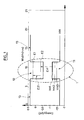
- Figure 2-b is a representation of a part of the diagram of figure 2-a showing in further detail the absorption layer 4 being located between the P-doped layer 5 and the avalanche layer 3.
- the absorption layer 4 being located between the P-doped layer 5 and the avalanche layer 3.
- Like elements of this figure are given like reference numerals as those of figure 2-a .
- intra-band photogenerated carriers 6 move out of the quantum wells 1 and become free electrons which are the injected into the avalanche layer 3.
- This is schematically represented in figure 2-b by means of arrows 7 showing the direction of displacement of the free electrons 6 towards the avalanche layer 3.
- the injection of the free electrons 6 in the avalanche layer allows for avalanche multiplication of the primary photocurrent, which improves the detector responsivity, to the extent that the responsivity is multiplied by a factor corresponding to the avalanche gain.
- the latter factor in the case of avalanche multiplication obtained by the injection of the free electrons 6 may be within the following range: 1 ⁇ M ⁇ 100.
- the SAGM structure with its field control layer allows an accurate distribution of the electric field with a high electric field in the avalanche layer, as needed for impact ionization process, while the electric field in the absorption layer remains low, thus favoring multiplication gain without excessive dark current.
- an optimized selection of well and barrier widths contribute to preventing dark current tunneling with an electric field in the small energy band-gap quantum wells (InGaAs) remaining below 160 kV/cm.
- the primary responsivity of the photodetector depends on the number of quantum wells and on their doping level because such doping provides the necessary free electrons for intra-band transition.
- SAGM APD with intra-band QWIP absorption layer allows up to 20 periods of InAlAs/InGaAs quantum wells, which is the same amount of InP/InGaAs quantum well periods currently known in the related art, where high responsivity was nevertheless achieved for the intra-band transition at 9 ⁇ m wavelength.
Landscapes
- Light Receiving Elements (AREA)
Abstract
Description
- The present invention relates to a photodetector for an optical device for use in applications such as DWDM optical transmission and free space optics (FSO). Other applications may include NIR (Near Infra-Red) remote sensing spectroscopy for chemical analysis and satellites or security-type applications such as night visions, homeland security, and the like.
- Photodetectors operating at a wavelength range from 1.6 µm to 2.6 µm at room temperature are being increasingly used in applications such as DWDM optical transmission at L-U/XL bands (up to 1.7 µm) and free space optics (FSO) systems for last mile cable-free high capacity connectivity for carrier applications where optimum overall performances are usually achieved in the 2.0-2.5 µm range (so-called atmospheric transmission window). Conventional photodetectors for this wavelength range are known to be made by using two main types of material systems: HgCdTe and InGaAs.
- HgCdTe photodetectors wavelength range can be tuned between 1 to 14 µm, which is a wide range for the applications identified above, depending on composition ratio of HgTe and CdTe. However, this technology suffers from the drawback that devices made based on HgCdTe generate excessive dark current, thus requiring an additional cooling mechanism in order to achieve good capability for photo-detection. However, the addition of a cooling mechanism is detrimental as it complicates the manufacturing of the device.
- The expression "dark current", in this context, refers to an electric current generated inside the photodetector device without the presence of photons, which is an undesirable effect in the photodetector, the expression being known to those skilled in the related art.
- As regard use of InGaAs material, photodiodes made with the known lattice-matched InxGa(1-x)As (x=0.53) grown on an InP substrate can be tailored so as to achieve a spectral bandwidth edge in a range between 1.65 µm and 2.6 µm, the range being obtainable by varying the x fraction in the alloy. However, here again a high dark current is generated due to a lattice-mismatched InAsP buffer layer which produces dislocations, i.e. crystalline defects, with the associated drawbacks.
- A further solution is based on the use of In0.83Ga0.17As multiple quantum wells, strain-compensated by In0.83Ga0.17P barrier layers. This solution allows to extend the cut-off wavelength up to 1.9 µm using inter-band transition. However, a large number of quantum well periods (in the order of 100 quantum wells) become necessary in order to achieve a good detector responsivity.
- The term "responsivity", in this context, refers to the ratio between the electrical output to the optical input of the device, the term being known to those skilled in the related art.
- A still further solution is based on the use of dual-band transition in InGaAs/InP quantum wells, namely intra-band and inter-band transition.
- The term "intra-band" refers to a type of transition in which an electron excited by an incident photon is made to move from a first level to a second level, the two levels being inside one single band, be it valence band or conduction band. The term "inter-band" in turn refers to the transition of an electron excited by an incident photon from a first level to a second level, where each of said levels is in a different band, for example a transition from the valence band to the conduction band or vice-versa. Both these terms are known to those skilled in the related art. However, the material properties of these quantum wells allow only transitions at wavelength of 1.1 µm in NIR and 9 µm in MIR (MIR standing for Mid-Infra-Red). Therefore by using this technique, the desired range of 1.6 µm to 2.6 µm is not covered. In addition, devices manufactured using this technique suffer from excessive leakage currents, thus requiring the photodetector to operate at only very low temperatures (typically around 77K).
- A still further known solution relates to photodetectors based on the use of type II inter-band transition in GaInAs/GaAsSb quantum wells. For this type of photodetectors, an operation wavelength of 2.3 µm is known. However, in this case, despite a large number of quantum well pairs present in the device, the photodetector responsivity remains low because of the low efficiency of type II transitions in quantum wells.
- It is therefore desired to provide a photodetector capable of operating at wavelengths in the range of 1.6 µm to 2.6 µm providing at the same time an improved level of responsivity as compared to the known devices, without suffering from the above-identified drawbacks.
- The above objective is reached by using the solution proposed by the present invention according to which intra-band transition is used between quantized states within the conduction band in InAlAs/InGaAs quantum wells in order to achieve an absorption wavelength in the desired range of 1.6 µm to 2.6 µm. Furthermore, in order to increase the responsivity of the device, the invention proposes the multiplication of the photogenerated electrons in a separate avalanche layer based on a separate absorption and multiplication (SAM) structure. The terms "photogenerated electron" refer to electrons and holes generated by absorption of the incident light.
- Accordingly one object of the present invention is that of providing a method for detecting wavelengths within a predefined range by a photodetector, comprising the step of performing a transition of electron energy by absorption of energy in response to an incident light, characterized by comprising the steps of:
- performing said transition in intra-band within a quantum well, between quantized levels in a conduction band; and
- performing multiplication of free electrons generated by said transition in an avalanche layer.
- According to an aspect of the invention, said predefined range of wavelength is between about 1.6 µm and about 2.6 µm.
- According to another aspect of the invention the wavelength is about 2.6 µm or about 2 µm.
- According to still another aspect of the invention the photodetector is built on a separate absorption grading and multiplication avalanche photodiode.
- According to a further aspect of the invention, intra-band photogenerated carriers move out of quantum wells, thus becoming free electrons which are the injected into the avalanche layer.
- Another object of the present invention is that of providing a photodetector for detecting wavelengths within a predefined range, using electron energy transition by absorption of energy in response to an incident light, characterized in that the photodetector is adapted to perform said transition in intra-band within a quantum well, between quantized levels in a conduction band, and to perform multiplication of free electrons generated by said transition in an avalanche layer.
- According to an aspect of the invention the photodetector is built on a separate absorption and multiplication avalanche photodiode.
- Preferably the photodetector is built on a separate absorption grading and multiplication avalanche photodiode.
- According to another aspect of the invention the quantum well of the photodetector has barrier layers, wherein the height and width of the barrier layers are selected so as to minimize a tunneling current.
- Preferably said width of the barrier layers is between 6 and 8 nm, and more preferably about 7 nm.
- Preferably said height of the barrier layers is between 0.5 eV and 0.9 eV.
- According to still another aspect of the invention said predefined range of wavelength is between about 1.6 µm and about 2.6 µm.
- According to yet another aspect of the invention the photodetector is further adapted to perform inter-band transition from an energy level in a valence band to an energy level in the conduction band.
- According to a further aspect of the invention a doping level of the charge present in the avalanche region is 4x1012 cm-2.
- According to still a further aspect of the invention the quantum well has a width of 4 nm and the wavelength is about 2 µm.
- According to yet a further aspect of the invention the quantum well has a width of 4.5 nm and the wavelength is about 2.3 µm.
- As a result of performing transition in intra-band between quantized states in a conduction band within a quantum well, an absorption at the predefined wavelength range is achieved.
- Furthermore, the multiplication of photogenerated electrons in an avalanche layer improves responsivity.
- These and further features and advantages of the present invention are described in more detail in the following description as well as in the claims with the aid of the accompanying drawings.
-
-
Figure 1 is a schematic energy-band diagram of a single quantum well absorption layer. -
Figure 2-a is a calculated energy band diagram of an SAGM APD with intra-band transition quantum wells absorption layer. -
Figure 2-b is a representation in part of the diagram offigure 2-a showing in further detail intra-band photogenerated carriers in the quantum wells being injected into the avalanche layer. - The device, according to the present invention is built on a separate absorption and multiplication (SAM) structure which is well-known in the art. Preferably, the device is built on the well known structure known as SAGM APD (SAGM standing for Separate Absorption Grading and Multiplication which is a specific variant of SAM with the particularity that in SAGM an additional layer is incorporated between absorption and multiplication with gradual composition which provides a gradual effect in the band-gap of the semi-conductor; APD standing for Avalanche Photodiode) where the absorption of incident light at the desired range of wavelengths is achieved by an intra-band transition in InAlAs/InGaAs quantum wells such as quantum well infrared photodetectors (QWIP). For known III-V type APDs, the structure is based on SAGM where multiplication and absorption take place in two different layers.
-
Figure 1 shows a schematic energy band diagram of a singlequantum well 1 according to the present invention. The diagram is shown on a coordinate axes of Energy in eV on the Y axis and width of the device in nm on the X axis. As shown in the figure, thequantum well 1 has two energy levels, or bands, one being thevalence band 11 and the other being theconduction band 12. In the figure only one quantum well is shown, however in practice further quantum wells adjacent to the one shown in the figure may exist, as will be observed in reference tofigures 2-a and 2-b . In the case of multiple quantum wells, the quantum wells are separated from each other by means of the so-called barriers. A barrier corresponds to the bulk of the semiconductor located between two neighboring quantum wells. Infigure 1 , barrier levels are represented byreference numeral 13. The distance separating two neighboring quantum wells corresponds to the width of the barrier separating the quantum well. - In the present example, the
quantum well 1 does not have a bias voltage applied thereto. Thevalence band 11 comprises energy levels shown in the figure by horizontal lines HH1, HH2 and HH3. The conduction band also comprises energy levels shown in the figure by horizontal lines E1 and E2. This is known in the related art. - According to the invention, upon the impact of an incident light, a bound-to-bound level transition of an electron occurs from a first energy level E1 to a second energy level E2 for an incident photon energy of E21, where:

- In this manner the transition of the excited electron is performed within the conduction band, and thereby an intra-band transition is obtained. This transition is shown in
figure 1 by the arrow E21. - In order to achieve one single transition E21 of interest with a corresponding wavelength within the desired range, for example 2.3 µm (E21 = 537 meV), the material composition and the width of the quantum well as well 1 as the those of the surrounding barrier(s) 13 are selected so as to provide optimum results. One preferred material composition for the quantum well is In0,72Ga0,28As. A preferred width for the quantum well is 4.5 nm with exx = -1.3% (exx standing for bi-axial strain and defined by the relationship exx=-Δa/a where a is the lattice-constant of the semi-conductor). A preferred material composition for the barrier is In0,3Al0,7GaAs and a preferred width for the barrier is in the range of 6-8 nm, and preferably 7 nm with exx = +1.50%.
- In a further example, a similar barrier width (7 nm) with exx= +1.5% is used, however with an In0,72Ga0,28As quantum well having the width of 4 nm (with exx= -1.3%). In this case, a single E21 transition of 2.0 µm wavelength (E21 = 606 meV) is produced which is also in the desired range.
- The photo-excited electrons, now in the E2 level, can therefore be swept out of the well by thermionic emission (thermally activated electrons) or by an applied voltage, resulting in free electrons which may then constitute a photocurrent, i.e. electric current generated as a result of a photon absorption.
- The absorption region response time is very small as it is limited only by the photoelectron response time (no hole response time is associated with this transition).
-
Figure 1 shows also a possible inter-band transition, namely a transition between thevalence band 11 and theconduction band 12. This is represented by the arrow EH showing a transition from the energy level HH1 in thevalence band 11 to energy level E2 in theconduction band 12. The wavelength is typically 1.5 µm. This structure thus allows for providing a dual band photodetector operation using InAlAs/InGaAs material system. - In order to avoid or minimize tunneling effect, which is undesirable, appropriate height and width for the
barrier layer 13 are selected. The preferred value of the width of the barrier level given above, i.e. in the range of 6-8 nm and preferably 7 nm, is also appropriate for this purpose. A preferred range for the height of the barrier level is between 0.5 eV to 0.9 eV. - In order to obtain an accurate electric field distribution along the detector structure, an appropriate doping level of the charge present in the avalanche region is to be selected. A typical value for an appropriate doping level of the charge in the avalanche region is 4x1012 cm-2. This prevents the presence of an excessive electric field in the absorption layer despite the fact that the quantum wells used are n-doped so as to provide free electrons which are confined in the well regions. Such characteristics allow to increase detector responsivity of incident light at wavelengths in the desired range m by multiplication gain without excessive dark current in the quantum well absorption layer.
-
Figure 2-a shows a calculated energy band diagram by simulation, with an applied bias of an SAGM APD with an absorption layer comprising ten quantum wells having the characteristics described above, and with intra-band transition at 2.3 µm. The diagram is shown on a coordinate axes of energy in eV on the Y axis and thickness of the device vertical structure in µm on the X axis. Starting from the substrate, on the bottom-right hand side of the diagram, the structure comprises an N-dopedInAlAs contact layer 2, a non-intentionally-dopedavalanche layer 3 of InAlAs material, a P-doped InAlAs charge layer (not shown), an InGaAlAs grading layer (not shown), followed by anabsorption layer 4 comprising tenquantum wells 1 of InGaAs/InAlAs material (as described above) and a P-dopedwindow layer 5 of InP material. The upper level energy line of the diagram,reference numeral 12, represents the conduction band energy level (in correspondence tofigure 1 ) and the lower level energy line thereof,reference numeral 11, represent the valence band level (also in correspondence tofigure 1 ). -
Figure 2-b is a representation of a part of the diagram offigure 2-a showing in further detail theabsorption layer 4 being located between the P-dopedlayer 5 and theavalanche layer 3. Like elements of this figure are given like reference numerals as those offigure 2-a . - According to the invention, intra-band
photogenerated carriers 6 move out of thequantum wells 1 and become free electrons which are the injected into theavalanche layer 3. This is schematically represented infigure 2-b by means ofarrows 7 showing the direction of displacement of thefree electrons 6 towards theavalanche layer 3. The injection of thefree electrons 6 in the avalanche layer allows for avalanche multiplication of the primary photocurrent, which improves the detector responsivity, to the extent that the responsivity is multiplied by a factor corresponding to the avalanche gain. Here, the primary photocurrent corresponds to the device photocurrent without avalanche gain, i.e. M=1, where M is the avalanche multiplication factor. The latter factor, in the case of avalanche multiplication obtained by the injection of thefree electrons 6 may be within the following range: 1 <M<100. - In this manner a photodetector is obtained which is capable of operating at wavelengths in the range of 1.6 µm to 2.6 µm, providing at the same time improved responsivity due to the avalanche multiplication gain.
- The SAGM structure with its field control layer (P-type charge layer) allows an accurate distribution of the electric field with a high electric field in the avalanche layer, as needed for impact ionization process, while the electric field in the absorption layer remains low, thus favoring multiplication gain without excessive dark current. In addition, as described above, an optimized selection of well and barrier widths contribute to preventing dark current tunneling with an electric field in the small energy band-gap quantum wells (InGaAs) remaining below 160 kV/cm.
- The primary responsivity of the photodetector depends on the number of quantum wells and on their doping level because such doping provides the necessary free electrons for intra-band transition. Presently, SAGM APD with intra-band QWIP absorption layer allows up to 20 periods of InAlAs/InGaAs quantum wells, which is the same amount of InP/InGaAs quantum well periods currently known in the related art, where high responsivity was nevertheless achieved for the intra-band transition at 9 µm wavelength.
Claims (17)
- Method for detecting wavelengths within a predefined range by a photodetector, comprising the step of performing a transition of electron energy by absorption of energy in response to an incident light, characterized by comprising the steps of:- performing said transition in intra-band within a quantum well (1), between quantized levels (E1, E2) in a conduction band (12); and- performing multiplication of free electrons (6) generated by said transition in an avalanche layer (3).
- A method according to claim 1, wherein said predefined range of wavelength is between about 1.6 µm and about 2.6 µm.
- A method according to claim 2, wherein the wavelength is about 2.6 µm.
- A method according to claim 2, wherein the wavelength is about 2 µm.
- A method according to any one of the preceding claims, wherein the photodetector is built on a separate absorption grading and multiplication avalanche photodiode.
- A method according to any one of the preceding claims, wherein intra-band photogenerated carriers (6) move out of quantum wells (1) thus becoming free electrons which are the injected into the avalanche layer (3).
- A photodetector for detecting wavelengths within a predefined range, using electron energy transition by absorption of energy in response to an incident light, characterized in that the photodetector is adapted to perform said transition in intra-band within a quantum well, between quantized levels (E1, E2) in a conduction band (12), and to perform multiplication of free electrons (6) generated by said transition in an avalanche layer (3).
- A photodetector according to claim 7, wherein the photodetector is built on a separate absorption and multiplication avalanche photodiode.
- A photodetector according to claim 8, wherein the photodetector is built on a separate absorption grading and multiplication avalanche photodiode.
- A photodetector according to any one of claims 7 to 9, wherein the quantum well (1) of the photodetector has barrier layers, wherein the height and width of the barrier layers are selected so as to minimize a tunneling current.
- A photodetector according to claim 10, wherein said width of the barrier layers is between 6 and 8 nm, preferably about 7 nm.
- A photodetector according to claim 10 or claim 11, wherein said height of the barrier layers is between 0.5 eV and 0.9 eV.
- A photodetector according to any one of the claims 7 to 12, wherein said predefined range of wavelength is between about 1.6 µm and about 2.6 µm.
- A photodetector according to any one of the claims 7 to 13, wherein the photodetector is further adapted to perform inter-band transition from an energy level (HH1) in a valence band (11) to an energy level (E2) in the conduction band (12).
- A photodetector according to any one of the claims 7 to 14, wherein a doping level of the charge present in the avalanche region is 4x1012 cm-2.
- A photodetector according to claim 13, wherein the quantum well has a width of 4 nm and the wavelength is about 2 µm.
- A photodetector according to claim 13, wherein the quantum well has a width of 4.5 nm and the wavelength is about 2.3 µm.
Priority Applications (1)
| Application Number | Priority Date | Filing Date | Title |
|---|---|---|---|
| EP07301386.4A EP2040307B1 (en) | 2007-09-20 | 2007-09-20 | A photodetector for an optical device |
Applications Claiming Priority (1)
| Application Number | Priority Date | Filing Date | Title |
|---|---|---|---|
| EP07301386.4A EP2040307B1 (en) | 2007-09-20 | 2007-09-20 | A photodetector for an optical device |
Publications (2)
| Publication Number | Publication Date |
|---|---|
| EP2040307A1 true EP2040307A1 (en) | 2009-03-25 |
| EP2040307B1 EP2040307B1 (en) | 2013-08-07 |
Family
ID=39145124
Family Applications (1)
| Application Number | Title | Priority Date | Filing Date |
|---|---|---|---|
| EP07301386.4A Not-in-force EP2040307B1 (en) | 2007-09-20 | 2007-09-20 | A photodetector for an optical device |
Country Status (1)
| Country | Link |
|---|---|
| EP (1) | EP2040307B1 (en) |
Citations (2)
| Publication number | Priority date | Publication date | Assignee | Title |
|---|---|---|---|---|
| US5121181A (en) | 1989-01-31 | 1992-06-09 | International Business Machines Corporation | Resonant tunneling photodetector for long wavelength applications |
| US20030047752A1 (en) | 2000-09-29 | 2003-03-13 | Campbell Joe C. | Avalanche photodiodes with an impact-ionization-engineered multiplication region |
-
2007
- 2007-09-20 EP EP07301386.4A patent/EP2040307B1/en not_active Not-in-force
Patent Citations (2)
| Publication number | Priority date | Publication date | Assignee | Title |
|---|---|---|---|---|
| US5121181A (en) | 1989-01-31 | 1992-06-09 | International Business Machines Corporation | Resonant tunneling photodetector for long wavelength applications |
| US20030047752A1 (en) | 2000-09-29 | 2003-03-13 | Campbell Joe C. | Avalanche photodiodes with an impact-ionization-engineered multiplication region |
Non-Patent Citations (2)
| Title |
|---|
| PAN J L ET AL: "Theory, fabrication and characterization of quantum well infrared photodetectors", MATERIALS SCIENCE AND ENGINEERING R: REPORTS, ELSEVIER SEQUOIA S.A., LAUSANNE, CH, vol. 28, no. 3-4, July 2000 (2000-07-01), pages 65 - 147, XP004201221, ISSN: 0927-796X * |
| ROGALSKI A: "Quantum well photoconductors in infrared detector technology", JOURNAL OF APPLIED PHYSICS, AMERICAN INSTITUTE OF PHYSICS. NEW YORK, US, vol. 93, no. 8, 15 April 2003 (2003-04-15), pages 4355 - 4391, XP012059396, ISSN: 0021-8979 * |
Also Published As
| Publication number | Publication date |
|---|---|
| EP2040307B1 (en) | 2013-08-07 |
Similar Documents
| Publication | Publication Date | Title |
|---|---|---|
| US7271405B2 (en) | Intersubband detector with avalanche multiplier region | |
| US6455908B1 (en) | Multispectral radiation detectors using strain-compensating superlattices | |
| US9887307B2 (en) | Diode barrier infrared detector devices and barrier superlattice structures | |
| EP2200096B1 (en) | Avalanche photodiode | |
| Rogalski | Comparison of the performance of quantum well and conventional bulk infrared photodetectors | |
| Martyniuk et al. | Interband quantum cascade infrared photodetectors: Current status and future trends | |
| US5457331A (en) | Dual-band infrared radiation detector optimized for fabrication in compositionally graded HgCdTe | |
| US5313073A (en) | Light detector using intersub-valence band transitions with strained barriers | |
| US20150179863A1 (en) | Avalanche photodiode utilizing interfacial misfit array | |
| Schönbein et al. | A 10 μm GaAs/Al x Ga1− x As intersubband photodetector operating at zero bias voltage | |
| Circir et al. | Optimization of in-device depleted passivation layer for InGaAs photodetectors | |
| Wang et al. | Photovoltaic and photoconductive dual‐mode operation GaAs quantum well infrared photodetector for two‐band detection | |
| Bansal et al. | Photodetectors for security application | |
| US20140217540A1 (en) | Fully depleted diode passivation active passivation architecture | |
| US6747296B1 (en) | Avalanche photodiode multiplication region and avalanche photodiode with low impact ionization rate ratio | |
| Uzgur et al. | InGaAs nBn SWIR detector design with lattice-matched InAlGaAs barrier | |
| US6965152B1 (en) | Broad-band quantum well infrared photodetectors | |
| Buffaz et al. | State of the art of quantum cascade photodetectors | |
| EP2040307B1 (en) | A photodetector for an optical device | |
| WO2014002082A2 (en) | Photodetector device | |
| Hostut et al. | Three-color broadband asymmetric quantum well infrared photodetectors in long wavelength infrared range (LWIR) | |
| Goh et al. | InAlAs avalanche photodiode with type-II absorber for detection beyond 2 μm | |
| EP2015366A1 (en) | Superlattice structure for photodetection incorporating coupled quantum dots | |
| Yuan et al. | Analysis of the detectivity for triple-layer heterojunction GaSb/GaInAsSb infrared detectors | |
| Rutkowski et al. | Two-colour HgCdTe infrared detectors operating above 200 K |
Legal Events
| Date | Code | Title | Description |
|---|---|---|---|
| PUAI | Public reference made under article 153(3) epc to a published international application that has entered the european phase |
Free format text: ORIGINAL CODE: 0009012 |
|
| AK | Designated contracting states |
Kind code of ref document: A1 Designated state(s): AT BE BG CH CY CZ DE DK EE ES FI FR GB GR HU IE IS IT LI LT LU LV MC MT NL PL PT RO SE SI SK TR |
|
| AX | Request for extension of the european patent |
Extension state: AL BA HR MK RS |
|
| 17P | Request for examination filed |
Effective date: 20090925 |
|
| 17Q | First examination report despatched |
Effective date: 20091104 |
|
| AKX | Designation fees paid |
Designated state(s): AT BE BG CH CY CZ DE DK EE ES FI FR GB GR HU IE IS IT LI LT LU LV MC MT NL PL PT RO SE SI SK TR |
|
| RAP1 | Party data changed (applicant data changed or rights of an application transferred) |
Owner name: ALCATEL LUCENT |
|
| GRAP | Despatch of communication of intention to grant a patent |
Free format text: ORIGINAL CODE: EPIDOSNIGR1 |
|
| GRAS | Grant fee paid |
Free format text: ORIGINAL CODE: EPIDOSNIGR3 |
|
| GRAA | (expected) grant |
Free format text: ORIGINAL CODE: 0009210 |
|
| AK | Designated contracting states |
Kind code of ref document: B1 Designated state(s): AT BE BG CH CY CZ DE DK EE ES FI FR GB GR HU IE IS IT LI LT LU LV MC MT NL PL PT RO SE SI SK TR |
|
| REG | Reference to a national code |
Ref country code: GB Ref legal event code: FG4D |
|
| REG | Reference to a national code |
Ref country code: CH Ref legal event code: EP Ref country code: AT Ref legal event code: REF Ref document number: 626090 Country of ref document: AT Kind code of ref document: T Effective date: 20130815 |
|
| REG | Reference to a national code |
Ref country code: IE Ref legal event code: FG4D |
|
| 111Z | Information provided on other rights and legal means of execution |
Free format text: AT BE BG CH CY CZ DE DK EE ES FI FR GB GR HU IE IS IT LI LT LU LV MC MT NL PL PT RO SE SI SK TR Effective date: 20130410 |
|
| REG | Reference to a national code |
Ref country code: DE Ref legal event code: R096 Ref document number: 602007032094 Country of ref document: DE Effective date: 20131002 |
|
| REG | Reference to a national code |
Ref country code: AT Ref legal event code: MK05 Ref document number: 626090 Country of ref document: AT Kind code of ref document: T Effective date: 20130807 |
|
| REG | Reference to a national code |
Ref country code: NL Ref legal event code: VDEP Effective date: 20130807 |
|
| REG | Reference to a national code |
Ref country code: LT Ref legal event code: MG4D |
|
| PG25 | Lapsed in a contracting state [announced via postgrant information from national office to epo] |
Ref country code: IS Free format text: LAPSE BECAUSE OF FAILURE TO SUBMIT A TRANSLATION OF THE DESCRIPTION OR TO PAY THE FEE WITHIN THE PRESCRIBED TIME-LIMIT Effective date: 20131207 Ref country code: SE Free format text: LAPSE BECAUSE OF FAILURE TO SUBMIT A TRANSLATION OF THE DESCRIPTION OR TO PAY THE FEE WITHIN THE PRESCRIBED TIME-LIMIT Effective date: 20130807 Ref country code: AT Free format text: LAPSE BECAUSE OF FAILURE TO SUBMIT A TRANSLATION OF THE DESCRIPTION OR TO PAY THE FEE WITHIN THE PRESCRIBED TIME-LIMIT Effective date: 20130807 Ref country code: PT Free format text: LAPSE BECAUSE OF FAILURE TO SUBMIT A TRANSLATION OF THE DESCRIPTION OR TO PAY THE FEE WITHIN THE PRESCRIBED TIME-LIMIT Effective date: 20131209 Ref country code: CY Free format text: LAPSE BECAUSE OF FAILURE TO SUBMIT A TRANSLATION OF THE DESCRIPTION OR TO PAY THE FEE WITHIN THE PRESCRIBED TIME-LIMIT Effective date: 20130731 Ref country code: LT Free format text: LAPSE BECAUSE OF FAILURE TO SUBMIT A TRANSLATION OF THE DESCRIPTION OR TO PAY THE FEE WITHIN THE PRESCRIBED TIME-LIMIT Effective date: 20130807 |
|
| PG25 | Lapsed in a contracting state [announced via postgrant information from national office to epo] |
Ref country code: SI Free format text: LAPSE BECAUSE OF FAILURE TO SUBMIT A TRANSLATION OF THE DESCRIPTION OR TO PAY THE FEE WITHIN THE PRESCRIBED TIME-LIMIT Effective date: 20130807 Ref country code: PL Free format text: LAPSE BECAUSE OF FAILURE TO SUBMIT A TRANSLATION OF THE DESCRIPTION OR TO PAY THE FEE WITHIN THE PRESCRIBED TIME-LIMIT Effective date: 20130807 Ref country code: LV Free format text: LAPSE BECAUSE OF FAILURE TO SUBMIT A TRANSLATION OF THE DESCRIPTION OR TO PAY THE FEE WITHIN THE PRESCRIBED TIME-LIMIT Effective date: 20130807 Ref country code: NL Free format text: LAPSE BECAUSE OF FAILURE TO SUBMIT A TRANSLATION OF THE DESCRIPTION OR TO PAY THE FEE WITHIN THE PRESCRIBED TIME-LIMIT Effective date: 20130807 Ref country code: BE Free format text: LAPSE BECAUSE OF FAILURE TO SUBMIT A TRANSLATION OF THE DESCRIPTION OR TO PAY THE FEE WITHIN THE PRESCRIBED TIME-LIMIT Effective date: 20130807 Ref country code: GR Free format text: LAPSE BECAUSE OF FAILURE TO SUBMIT A TRANSLATION OF THE DESCRIPTION OR TO PAY THE FEE WITHIN THE PRESCRIBED TIME-LIMIT Effective date: 20131108 Ref country code: FI Free format text: LAPSE BECAUSE OF FAILURE TO SUBMIT A TRANSLATION OF THE DESCRIPTION OR TO PAY THE FEE WITHIN THE PRESCRIBED TIME-LIMIT Effective date: 20130807 |
|
| PG25 | Lapsed in a contracting state [announced via postgrant information from national office to epo] |
Ref country code: CY Free format text: LAPSE BECAUSE OF FAILURE TO SUBMIT A TRANSLATION OF THE DESCRIPTION OR TO PAY THE FEE WITHIN THE PRESCRIBED TIME-LIMIT Effective date: 20130807 |
|
| PG25 | Lapsed in a contracting state [announced via postgrant information from national office to epo] |
Ref country code: SK Free format text: LAPSE BECAUSE OF FAILURE TO SUBMIT A TRANSLATION OF THE DESCRIPTION OR TO PAY THE FEE WITHIN THE PRESCRIBED TIME-LIMIT Effective date: 20130807 Ref country code: EE Free format text: LAPSE BECAUSE OF FAILURE TO SUBMIT A TRANSLATION OF THE DESCRIPTION OR TO PAY THE FEE WITHIN THE PRESCRIBED TIME-LIMIT Effective date: 20130807 Ref country code: DK Free format text: LAPSE BECAUSE OF FAILURE TO SUBMIT A TRANSLATION OF THE DESCRIPTION OR TO PAY THE FEE WITHIN THE PRESCRIBED TIME-LIMIT Effective date: 20130807 Ref country code: RO Free format text: LAPSE BECAUSE OF FAILURE TO SUBMIT A TRANSLATION OF THE DESCRIPTION OR TO PAY THE FEE WITHIN THE PRESCRIBED TIME-LIMIT Effective date: 20130807 Ref country code: CZ Free format text: LAPSE BECAUSE OF FAILURE TO SUBMIT A TRANSLATION OF THE DESCRIPTION OR TO PAY THE FEE WITHIN THE PRESCRIBED TIME-LIMIT Effective date: 20130807 |
|
| REG | Reference to a national code |
Ref country code: CH Ref legal event code: PL |
|
| PG25 | Lapsed in a contracting state [announced via postgrant information from national office to epo] |
Ref country code: MC Free format text: LAPSE BECAUSE OF FAILURE TO SUBMIT A TRANSLATION OF THE DESCRIPTION OR TO PAY THE FEE WITHIN THE PRESCRIBED TIME-LIMIT Effective date: 20130807 Ref country code: ES Free format text: LAPSE BECAUSE OF FAILURE TO SUBMIT A TRANSLATION OF THE DESCRIPTION OR TO PAY THE FEE WITHIN THE PRESCRIBED TIME-LIMIT Effective date: 20130807 Ref country code: IT Free format text: LAPSE BECAUSE OF FAILURE TO SUBMIT A TRANSLATION OF THE DESCRIPTION OR TO PAY THE FEE WITHIN THE PRESCRIBED TIME-LIMIT Effective date: 20130807 |
|
| PLBE | No opposition filed within time limit |
Free format text: ORIGINAL CODE: 0009261 |
|
| STAA | Information on the status of an ep patent application or granted ep patent |
Free format text: STATUS: NO OPPOSITION FILED WITHIN TIME LIMIT |
|
| REG | Reference to a national code |
Ref country code: IE Ref legal event code: MM4A |
|
| 26N | No opposition filed |
Effective date: 20140508 |
|
| PG25 | Lapsed in a contracting state [announced via postgrant information from national office to epo] |
Ref country code: CH Free format text: LAPSE BECAUSE OF NON-PAYMENT OF DUE FEES Effective date: 20130930 Ref country code: LI Free format text: LAPSE BECAUSE OF NON-PAYMENT OF DUE FEES Effective date: 20130930 Ref country code: IE Free format text: LAPSE BECAUSE OF NON-PAYMENT OF DUE FEES Effective date: 20130920 |
|
| REG | Reference to a national code |
Ref country code: DE Ref legal event code: R097 Ref document number: 602007032094 Country of ref document: DE Effective date: 20140508 |
|
| PG25 | Lapsed in a contracting state [announced via postgrant information from national office to epo] |
Ref country code: TR Free format text: LAPSE BECAUSE OF FAILURE TO SUBMIT A TRANSLATION OF THE DESCRIPTION OR TO PAY THE FEE WITHIN THE PRESCRIBED TIME-LIMIT Effective date: 20130807 Ref country code: MT Free format text: LAPSE BECAUSE OF FAILURE TO SUBMIT A TRANSLATION OF THE DESCRIPTION OR TO PAY THE FEE WITHIN THE PRESCRIBED TIME-LIMIT Effective date: 20130807 |
|
| PG25 | Lapsed in a contracting state [announced via postgrant information from national office to epo] |
Ref country code: LU Free format text: LAPSE BECAUSE OF NON-PAYMENT OF DUE FEES Effective date: 20130920 Ref country code: BG Free format text: LAPSE BECAUSE OF FAILURE TO SUBMIT A TRANSLATION OF THE DESCRIPTION OR TO PAY THE FEE WITHIN THE PRESCRIBED TIME-LIMIT Effective date: 20130807 Ref country code: HU Free format text: LAPSE BECAUSE OF FAILURE TO SUBMIT A TRANSLATION OF THE DESCRIPTION OR TO PAY THE FEE WITHIN THE PRESCRIBED TIME-LIMIT; INVALID AB INITIO Effective date: 20070920 |
|
| REG | Reference to a national code |
Ref country code: FR Ref legal event code: PLFP Year of fee payment: 9 |
|
| REG | Reference to a national code |
Ref country code: FR Ref legal event code: PLFP Year of fee payment: 10 |
|
| REG | Reference to a national code |
Ref country code: FR Ref legal event code: PLFP Year of fee payment: 11 |
|
| PGFP | Annual fee paid to national office [announced via postgrant information from national office to epo] |
Ref country code: GB Payment date: 20170921 Year of fee payment: 11 Ref country code: FR Payment date: 20170928 Year of fee payment: 11 Ref country code: DE Payment date: 20170928 Year of fee payment: 11 |
|
| REG | Reference to a national code |
Ref country code: DE Ref legal event code: R119 Ref document number: 602007032094 Country of ref document: DE |
|
| GBPC | Gb: european patent ceased through non-payment of renewal fee |
Effective date: 20180920 |
|
| REG | Reference to a national code |
Ref country code: GB Ref legal event code: 732E Free format text: REGISTERED BETWEEN 20190429 AND 20190502 |
|
| REG | Reference to a national code |
Ref country code: DE Ref legal event code: R082 Ref document number: 602007032094 Country of ref document: DE Representative=s name: MENZIETTI WETZEL, DE Ref country code: DE Ref legal event code: R081 Ref document number: 602007032094 Country of ref document: DE Owner name: PROVENANCE ASSET GROUP LLC, PITTSFORD, US Free format text: FORMER OWNER: ALCATEL LUCENT, PARIS, FR |
|
| PG25 | Lapsed in a contracting state [announced via postgrant information from national office to epo] |
Ref country code: DE Free format text: LAPSE BECAUSE OF NON-PAYMENT OF DUE FEES Effective date: 20190402 |
|
| PG25 | Lapsed in a contracting state [announced via postgrant information from national office to epo] |
Ref country code: FR Free format text: LAPSE BECAUSE OF NON-PAYMENT OF DUE FEES Effective date: 20180930 |
|
| PG25 | Lapsed in a contracting state [announced via postgrant information from national office to epo] |
Ref country code: GB Free format text: LAPSE BECAUSE OF NON-PAYMENT OF DUE FEES Effective date: 20180920 |