EP2037315A2 - LCD display with LED backlight optimized for minimum notebook computer dimensions - Google Patents
LCD display with LED backlight optimized for minimum notebook computer dimensions Download PDFInfo
- Publication number
- EP2037315A2 EP2037315A2 EP08015833A EP08015833A EP2037315A2 EP 2037315 A2 EP2037315 A2 EP 2037315A2 EP 08015833 A EP08015833 A EP 08015833A EP 08015833 A EP08015833 A EP 08015833A EP 2037315 A2 EP2037315 A2 EP 2037315A2
- Authority
- EP
- European Patent Office
- Prior art keywords
- display
- assembly
- display panel
- board
- panel
- Prior art date
- Legal status (The legal status is an assumption and is not a legal conclusion. Google has not performed a legal analysis and makes no representation as to the accuracy of the status listed.)
- Granted
Links
Images


Classifications
-
- G—PHYSICS
- G06—COMPUTING OR CALCULATING; COUNTING
- G06F—ELECTRIC DIGITAL DATA PROCESSING
- G06F1/00—Details not covered by groups G06F3/00 - G06F13/00 and G06F21/00
- G06F1/16—Constructional details or arrangements
- G06F1/1613—Constructional details or arrangements for portable computers
- G06F1/1633—Constructional details or arrangements of portable computers not specific to the type of enclosures covered by groups G06F1/1615 - G06F1/1626
- G06F1/1637—Details related to the display arrangement, including those related to the mounting of the display in the housing
-
- G—PHYSICS
- G06—COMPUTING OR CALCULATING; COUNTING
- G06F—ELECTRIC DIGITAL DATA PROCESSING
- G06F1/00—Details not covered by groups G06F3/00 - G06F13/00 and G06F21/00
- G06F1/16—Constructional details or arrangements
- G06F1/1613—Constructional details or arrangements for portable computers
- G06F1/1615—Constructional details or arrangements for portable computers with several enclosures having relative motions, each enclosure supporting at least one I/O or computing function
- G06F1/1616—Constructional details or arrangements for portable computers with several enclosures having relative motions, each enclosure supporting at least one I/O or computing function with folding flat displays, e.g. laptop computers or notebooks having a clamshell configuration, with body parts pivoting to an open position around an axis parallel to the plane they define in closed position
-
- G—PHYSICS
- G02—OPTICS
- G02F—OPTICAL DEVICES OR ARRANGEMENTS FOR THE CONTROL OF LIGHT BY MODIFICATION OF THE OPTICAL PROPERTIES OF THE MEDIA OF THE ELEMENTS INVOLVED THEREIN; NON-LINEAR OPTICS; FREQUENCY-CHANGING OF LIGHT; OPTICAL LOGIC ELEMENTS; OPTICAL ANALOGUE/DIGITAL CONVERTERS
- G02F1/00—Devices or arrangements for the control of the intensity, colour, phase, polarisation or direction of light arriving from an independent light source, e.g. switching, gating or modulating; Non-linear optics
- G02F1/01—Devices or arrangements for the control of the intensity, colour, phase, polarisation or direction of light arriving from an independent light source, e.g. switching, gating or modulating; Non-linear optics for the control of the intensity, phase, polarisation or colour
- G02F1/13—Devices or arrangements for the control of the intensity, colour, phase, polarisation or direction of light arriving from an independent light source, e.g. switching, gating or modulating; Non-linear optics for the control of the intensity, phase, polarisation or colour based on liquid crystals, e.g. single liquid crystal display cells
- G02F1/133—Constructional arrangements; Operation of liquid crystal cells; Circuit arrangements
- G02F1/1333—Constructional arrangements; Manufacturing methods
- G02F1/1345—Conductors connecting electrodes to cell terminals
- G02F1/13452—Conductors connecting driver circuitry and terminals of panels
Definitions
- the present invention relates to information handling systems and more particularly to information handling systems that comprise a liquid crystal display (LCD) with light-emitting diode (LED) backlight.
- LCD liquid crystal display
- LED light-emitting diode
- An information handling system generally processes, compiles, stores, and/or communicates information or data for business, personal, or other purposes thereby allowing users to take advantage of the value of the information.
- information handling systems may also vary regarding what information is handled, how the information is handled, how much information is processed, stored, or communicated, and how quickly and efficiently the information may be processed, stored, or communicated.
- the variations in information handling systems allow for information handling systems to be general or configured for a specific user or specific use such as financial transaction processing, airline reservations, enterprise data storage, or global communications.
- information handling systems may include a variety of hardware and software components that may be configured to process, store, and communicate information and may include one or more computer systems, data storage systems, and networking systems.
- LCD type displays include LCD panels that utilize an illumination system that is known as a backlight illumination system.
- the backlight illumination system is via a cold cathode fluorescent lamps (CCFL) bulb.
- CCFL cold cathode fluorescent lamps
- Certain LCD panels are now using LEDs for backlight illumination.
- a driver board for the LCD backlight assembly traverses the entire width of the LCD glass to allow flexible circuits to connect to the glass.
- Known notebook display assemblies include a chassis, an LCD panel, an LED driver board, and hinges to connect the display assembly to the base of the notebook information handling system.
- the hinges are generally positioned in the bottom left and right corners of the display assembly.
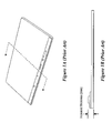
- One issue relating to known LED driver boards is that to minimize the thickness of an LCD assembly, the driver board is often positioned below the glass panel (see e.g., Figures 1A and 1B , labeled Prior Art).
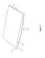
- the driver board and the hinges are often positioned in the same location. Either to rectify interference of the driver board and the hinges, the system can be made larger in the Y-dimension or the driver board can be placed behind the glass panel (see e.g., Figures 2A and 2B , labeled Prior Art).
- the result of placing the driver board (which is populated with components for driving the LED backlight illumination system) behind the panel is that the Z-dimension of the display assembly is increased (e.g., by about 3mm in the location of the driver board).
- a system and method that allows a LED driver board to both traverse the full width of the LCD glass and not occupy the volume occupied by the hinges is set forth. More specifically, by providing an LCD type display that includes an LED backlight illumination system, the LED driver board for a panel may be moved to the bottom side of a display assembly.
- the invention relates to an information handling system display assembly includes a display panel having a width, a display board assembly coupled to the processor and the display panel.
- the display board assembly includes a display board assembly coupled to the display panel on a display panel side of the display board and the display board has a wider portion extending the substantially width of the display panel and a narrow portion extending less than the width of the display panel, and a display component mounted on the display panel side of the display board.
- the invention in another embodiment, relates to an information handling system display assembly that includes a processor, memory coupled to the processor, and a display assembly.
- the display assembly includes a display panel having a width, a display board assembly coupled to the processor and the display panel.
- the display board assembly includes a display board assembly coupled to the display panel on a display panel side of the display board and the display board has a wider portion extending the substantially width of the display panel and a narrow portion extending less than the width of the display panel, and a display component mounted on the display panel side of the display board.
- the information handling system 300 includes a processor 302, input/output (I/O) devices 304, such as a display, a keyboard, a mouse, and associated controllers, memory 306, including volatile memory such as random access memory (RAM) and non-volatile memory such as read only memory (ROM) and hard disk drives, and other storage devices 308, such as an optical disk and drive, and various other subsystems 310, all interconnected via one or more buses 312.
- I/O devices 304 include an LCD display device 320
- an information handling system may include any instrumentality or aggregate of instrumentalities operable to compute, classify, process, transmit, receive, retrieve, originate, switch, store, display, manifest, detect, record, reproduce, handle, or utilize any form of information, intelligence, or data for business, scientific, control, or other purposes.
- an information handling system may be a personal computer, a network storage device, or any other suitable device and may vary in size, shape, performance, functionality, and price.
- the information handling system may include random access memory (RAM), one or more processing resources such as a central processing unit (CPU) or hardware or software control logic, ROM, and/or other types of nonvolatile memory.
- Additional components of the information handling system may include one or more disk drives, one or more network ports for communicating with external devices as well as various input and output (I/O) devices, such as a keyboard, a mouse, and a video display.
- the information handling system may also include one or more buses operable to transmit communications between the various hardware components.
- the LCD display device 320 includes an LCD panel 410 as well as a driver board assembly 420.
- the driver board assembly 420 includes an LED driver board 430 (which may be a printed circuit board) as well as components 440 mounted to the driver board 430.
- the LED driver board 430 is a thickness of, e.g., approximately 0.8mm.
- the total thickness of the driver board assembly 420 is, e.g., approximately 3.0mm.
- the LED driver board 430 is configured in a T shape.
- the wide portion 510 of the T of the LED driver board 430 i.e., the top of the T
- the under side 512 of the T cross bar is substantially flush with the bottom edge 620 of the glass of the LCD panel 410.
- the vertical portion 520 of the T (i.e., the base of the T) of the LED driver board protrudes below the bottom edge 620 of the glass.
- Components 440 of the LCD driver board assembly 420 are located on the portion 630 of the driver board assembly that protrudes below the edge 620 of the glass panel.
- the component portion of the driver board assembly need not traverse the entire width of the glass and can therefore be narrower than the width of the wider portion of the board. Accordingly, the portion of the driver board assembly that protrudes below the edge of the glass panel does not occupy the volume 460 of the panel assembly needed for the hinges. Le., the T shape of the diver board defines spaces into which the hinges may be positioned.
- This panel design allows the Y-dimension of the display assembly to be minimized to the dimension of the LCD glass plus the Y-dimension of the hinge volume.
- the display assembly thickness is only impacted by the 0.8mm addition of the LCD driver board that traverses behind the glass panel 410.
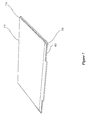
- FIG. 7 a perspective view of an LCD panel assembly including a wire channel is shown. More specifically, a light guide that is placed behind the LCD glass is utilized to illuminate the active area of the LCD glass. Often, there is unused (i.e., dead space) around the perimeter of the LCD glass for electrical connections and sealing of the glass panels (in certain embodiments, this space is approximately 5 mm). In certain embodiments, the light guide is reduced in size by approximately 4mm per side to create a channel 710 on the left and right sides of the panel 410. These channels can then be used for display assembly wire management.
- many notebook information handling systems have antennas positioned along the top edge of a display assembly.
- the wires that connect the antennas to the system base are coaxial wires that are 1.4mm in diameter.
- the non-populated driver board that traverses behind the LCD panel is 0.8mm thickness.
- the light guide has a thickness of approximately 1.2mm. By decreasing the total width of the light guide, a wire channel with a depth of about 2mm is created allowing for antenna wire runs 720 to the top edge of the display without affecting any of the display dimensions.
- the illumination LEDs may be mounted directly to the driver board 420.
- Right angle LEDs mounted to the component side of the driver board are in the correct orientation to illuminate the edge of the light guide that is placed behind the LCD glass 410.
Landscapes
- Engineering & Computer Science (AREA)
- Computer Hardware Design (AREA)
- Theoretical Computer Science (AREA)
- Physics & Mathematics (AREA)
- Human Computer Interaction (AREA)
- General Engineering & Computer Science (AREA)
- General Physics & Mathematics (AREA)
- Mathematical Physics (AREA)
- Devices For Indicating Variable Information By Combining Individual Elements (AREA)
- Liquid Crystal (AREA)
Abstract
Description
- The present invention relates to information handling systems and more particularly to information handling systems that comprise a liquid crystal display (LCD) with light-emitting diode (LED) backlight.
- As the value and use of information continues to increase, individuals and businesses seek additional ways to process and store information. One option available to users is information handling systems. An information handling system generally processes, compiles, stores, and/or communicates information or data for business, personal, or other purposes thereby allowing users to take advantage of the value of the information. Because technology and information handling needs and requirements vary between different users or applications, information handling systems may also vary regarding what information is handled, how the information is handled, how much information is processed, stored, or communicated, and how quickly and efficiently the information may be processed, stored, or communicated. The variations in information handling systems allow for information handling systems to be general or configured for a specific user or specific use such as financial transaction processing, airline reservations, enterprise data storage, or global communications. In addition, information handling systems may include a variety of hardware and software components that may be configured to process, store, and communicate information and may include one or more computer systems, data storage systems, and networking systems.
- It is known to provide portable information handling systems (such as notebook information handling systems) with LCD type displays. LCD type displays include LCD panels that utilize an illumination system that is known as a backlight illumination system. With known LCD panels, the backlight illumination system is via a cold cathode fluorescent lamps (CCFL) bulb. Certain LCD panels are now using LEDs for backlight illumination. With known LCD panels that use LEDs for backlight illumination, a driver board for the LCD backlight assembly traverses the entire width of the LCD glass to allow flexible circuits to connect to the glass.
- Known notebook display assemblies include a chassis, an LCD panel, an LED driver board, and hinges to connect the display assembly to the base of the notebook information handling system. The hinges are generally positioned in the bottom left and right corners of the display assembly. One issue relating to known LED driver boards is that to minimize the thickness of an LCD assembly, the driver board is often positioned below the glass panel (see e.g.,
Figures 1A and 1B , labeled Prior Art). - In known information handling systems, the driver board and the hinges are often positioned in the same location. Either to rectify interference of the driver board and the hinges, the system can be made larger in the Y-dimension or the driver board can be placed behind the glass panel (see e.g.,
Figures 2A and 2B , labeled Prior Art). The result of placing the driver board (which is populated with components for driving the LED backlight illumination system) behind the panel is that the Z-dimension of the display assembly is increased (e.g., by about 3mm in the location of the driver board). - Accordingly, it is desirable to provide a method that allows a LED driver board to both traverse the full width of the LCD glass and not occupy the volume occupied by the hinges.
- In accordance with the present invention a system and method that allows a LED driver board to both traverse the full width of the LCD glass and not occupy the volume occupied by the hinges is set forth. More specifically, by providing an LCD type display that includes an LED backlight illumination system, the LED driver board for a panel may be moved to the bottom side of a display assembly.
- In one embodiment, the invention relates to an information handling system display assembly includes a display panel having a width, a display board assembly coupled to the processor and the display panel. The display board assembly includes a display board assembly coupled to the display panel on a display panel side of the display board and the display board has a wider portion extending the substantially width of the display panel and a narrow portion extending less than the width of the display panel, and a display component mounted on the display panel side of the display board.
- In another embodiment, the invention relates to an information handling system display assembly that includes a processor, memory coupled to the processor, and a display assembly. The display assembly includes a display panel having a width, a display board assembly coupled to the processor and the display panel. The display board assembly includes a display board assembly coupled to the display panel on a display panel side of the display board and the display board has a wider portion extending the substantially width of the display panel and a narrow portion extending less than the width of the display panel, and a display component mounted on the display panel side of the display board.
- The present invention may be better understood, and its numerous objects, features, and advantages made apparent to those skilled in the art by referencing the accompanying drawings. The use of the same reference number throughout the several figures designates a like or similar element.
- Figures 1A and 1B
- labeled Prior Art, show a perspective view and a cross sectional view of a display driver printed circuit board positioned below an LCD panel.
- Figure 2A and 2B,
- labeled Prior Art, show a perspective view and a cross sectional view of a display driver printed circuit board layered with an LCD panel.
- Figure 3
- shows a system block diagram of an information handling system.
- Figure 4
- shows a front perspective view of an LCD panel assembly.
- Figure 5
- shows a rear perspective view of an LCD panel assembly.
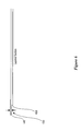
- Figure 6
- shows a cross section view of an LCD panel assembly.
- Figure 7
- shows a perspective view of an LCD panel assembly including a wire channel.
- Referring briefly to
Figure 3 , a system block diagram of aninformation handling system 300 is shown. Theinformation handling system 300 includes aprocessor 302, input/output (I/O)devices 304, such as a display, a keyboard, a mouse, and associated controllers,memory 306, including volatile memory such as random access memory (RAM) and non-volatile memory such as read only memory (ROM) and hard disk drives, andother storage devices 308, such as an optical disk and drive, and various other subsystems 310, all interconnected via one or more buses 312. The I/O devices 304 include anLCD display device 320 - For purposes of this disclosure, an information handling system may include any instrumentality or aggregate of instrumentalities operable to compute, classify, process, transmit, receive, retrieve, originate, switch, store, display, manifest, detect, record, reproduce, handle, or utilize any form of information, intelligence, or data for business, scientific, control, or other purposes. For example, an information handling system may be a personal computer, a network storage device, or any other suitable device and may vary in size, shape, performance, functionality, and price. The information handling system may include random access memory (RAM), one or more processing resources such as a central processing unit (CPU) or hardware or software control logic, ROM, and/or other types of nonvolatile memory. Additional components of the information handling system may include one or more disk drives, one or more network ports for communicating with external devices as well as various input and output (I/O) devices, such as a keyboard, a mouse, and a video display. The information handling system may also include one or more buses operable to transmit communications between the various hardware components.
- Referring to
Figures 4 - 6 , theLCD display device 320 includes anLCD panel 410 as well as adriver board assembly 420. Thedriver board assembly 420 includes an LED driver board 430 (which may be a printed circuit board) as well ascomponents 440 mounted to thedriver board 430. - The
LED driver board 430 is a thickness of, e.g., approximately 0.8mm. When components 610 are mounted on theLED driver board 430, the total thickness of thedriver board assembly 420 is, e.g., approximately 3.0mm. - The
LED driver board 430 is configured in a T shape. Thewide portion 510 of the T of the LED driver board 430 (i.e., the top of the T) traverses the width of theLCD panel 410. The underside 512 of the T cross bar is substantially flush with the bottom edge 620 of the glass of theLCD panel 410. Thevertical portion 520 of the T (i.e., the base of the T) of the LED driver board protrudes below the bottom edge 620 of the glass.Components 440 of the LCDdriver board assembly 420 are located on theportion 630 of the driver board assembly that protrudes below the edge 620 of the glass panel. The component portion of the driver board assembly need not traverse the entire width of the glass and can therefore be narrower than the width of the wider portion of the board. Accordingly, the portion of the driver board assembly that protrudes below the edge of the glass panel does not occupy thevolume 460 of the panel assembly needed for the hinges. Le., the T shape of the diver board defines spaces into which the hinges may be positioned. - This panel design allows the Y-dimension of the display assembly to be minimized to the dimension of the LCD glass plus the Y-dimension of the hinge volume. The display assembly thickness is only impacted by the 0.8mm addition of the LCD driver board that traverses behind the
glass panel 410. - Referring to
Figure 7 , a perspective view of an LCD panel assembly including a wire channel is shown. More specifically, a light guide that is placed behind the LCD glass is utilized to illuminate the active area of the LCD glass. Often, there is unused (i.e., dead space) around the perimeter of the LCD glass for electrical connections and sealing of the glass panels (in certain embodiments, this space is approximately 5 mm). In certain embodiments, the light guide is reduced in size by approximately 4mm per side to create achannel 710 on the left and right sides of thepanel 410. These channels can then be used for display assembly wire management. - Additionally, many notebook information handling systems have antennas positioned along the top edge of a display assembly. The wires that connect the antennas to the system base are coaxial wires that are 1.4mm in diameter. The non-populated driver board that traverses behind the LCD panel is 0.8mm thickness. The light guide has a thickness of approximately 1.2mm. By decreasing the total width of the light guide, a wire channel with a depth of about 2mm is created allowing for antenna wire runs 720 to the top edge of the display without affecting any of the display dimensions.
- The present invention is well adapted to attain the advantages mentioned as well as others inherent therein. While the present invention has been depicted, described, and is defined by reference to particular embodiments of the invention, such references do not imply a limitation on the invention, and no such limitation is to be inferred. The invention is capable of considerable modification, alteration, and equivalents in form and function, as will occur to those ordinarily skilled in the pertinent arts. The depicted and described embodiments are examples only, and are not exhaustive of the scope of the invention.
- For example, in certain embodiments, the illumination LEDs may be mounted directly to the
driver board 420. Right angle LEDs mounted to the component side of the driver board are in the correct orientation to illuminate the edge of the light guide that is placed behind theLCD glass 410. - Consequently, the invention is intended to be limited only by the spirit and scope of the appended claims, giving full cognizance to equivalents in all respects.
Claims (12)
- An information handling system display assembly comprising:a display panel, the display panel having a width;a display board assembly, the display board assembly being coupled to the display panel, the display board assembly comprisinga display board, the display board assembly being coupled to the display panel on a display panel side of the display board, the display board having a wider portion extending the substantially width of the display panel and a narrow portion extending less than the width of the display panel; and,a display component, the display component being mounted on the display panel side of the display board.
- The information handling system display assembly of claim 1 wherein:the display panel comprises a depth; and,when the display component is mounted on the display board, the display component protrudes no further than the depth of the display panel.
- The information handling system display assembly of claim 1 wherein:the display board corresponds to a T shape, the T shape having a top and a base; and,the wider portion of the display panel corresponds to the top of the T shape and the narrower portion of the display panel corresponds to the base of the T shape.
- The information handling system display assembly of claim 1 wherein:the wider portion of the display board and the narrower portion of the display board are contiguous; and,intersection of the wider portion of the display board and the narrower portion of the display board defines spaces into which hinges may be positioned.
- The information handling system display assembly of claim 1 further comprising:a display assembly housing, the display panel being mounted within the display assembly housing, the display assembly housing having a width, the width of the display assembly housing being greater than the width of the display panel and defining a channel; and whereinan antenna is positioned within the channel.
- The information handling system display assembly of claim 1 wherein:the display panel comprises a liquid crystal display (LCD) panel.
- An information handling system display assembly comprising:a processor;memory coupled to the processor; and,a display assembly, the display assembly comprisinga display panel, the display panel having a width;a display board assembly, the display board assembly being coupled to the processor and the display panel, the display board assembly comprisinga display board, the display board assembly being coupled to the display panel on a display panel side of the display board, the display board having a wider portion extending the substantially width of the display panel and a narrow portion extending less than the width of the display panel; and,a display component, the display component being mounted on the display panel side of the display board.
- The information handling system of claim 7 wherein:the display panel comprises a depth; and,when the display component is mounted on the display board, the display component protrudes no further than the depth of the display panel.
- The information handling system of claim 7 wherein:the display board corresponds to a T shape, the T shape having a top and a base; and,the wider portion of the display panel corresponds to the top of the T shape and the narrower portion of the display panel corresponds to the base of the T shape.
- The information handling system of claim 7 wherein:the wider portion of the display board and the narrower portion of the display board are contiguous; and,intersection of the wider portion of the display board and the narrower portion of the display board defines spaces into which hinges may be positioned.
- The information handling system of claim 7 wherein the display assembly further comprises:a display assembly housing, the display panel being mounted within the display assembly housing, the display assembly housing having a width, the width of the display assembly housing being greater than the width of the display panel and defining a channel; and whereinan antenna is positioned within the channel.
- The information handling system of claim 7 wherein:the display panel comprises a liquid crystal display (LCD) panel.
Applications Claiming Priority (1)
| Application Number | Priority Date | Filing Date | Title |
|---|---|---|---|
| US11/853,911 US20090066873A1 (en) | 2007-09-12 | 2007-09-12 | LCD Display with LED Backlight Optimized for Minimum Notebook Computer Dimensions |
Publications (3)
| Publication Number | Publication Date |
|---|---|
| EP2037315A2 true EP2037315A2 (en) | 2009-03-18 |
| EP2037315A3 EP2037315A3 (en) | 2010-02-24 |
| EP2037315B1 EP2037315B1 (en) | 2016-08-31 |
Family
ID=40130560
Family Applications (1)
| Application Number | Title | Priority Date | Filing Date |
|---|---|---|---|
| EP08015833.0A Active EP2037315B1 (en) | 2007-09-12 | 2008-09-09 | Notebook |
Country Status (5)
| Country | Link |
|---|---|
| US (1) | US20090066873A1 (en) |
| EP (1) | EP2037315B1 (en) |
| CN (1) | CN101398704A (en) |
| SG (1) | SG151208A1 (en) |
| TW (1) | TWI460575B (en) |
Families Citing this family (3)
| Publication number | Priority date | Publication date | Assignee | Title |
|---|---|---|---|---|
| US8408780B2 (en) * | 2009-11-03 | 2013-04-02 | Apple Inc. | Portable computer housing with integral display |
| US20110242039A1 (en) * | 2010-03-30 | 2011-10-06 | Garmin Ltd. | Display module for a touchscreen display |
| US10247972B2 (en) | 2013-06-19 | 2019-04-02 | Dell Products L.P. | Ultra-thin display assembly with integrated touch functionality |
Citations (5)
| Publication number | Priority date | Publication date | Assignee | Title |
|---|---|---|---|---|
| JP2000058998A (en) | 1998-08-07 | 2000-02-25 | Matsushita Electric Ind Co Ltd | TCP and liquid crystal display |
| WO2001046809A1 (en) | 1999-12-20 | 2001-06-28 | Telefonaktiebolaget Lm Ericsson (Publ) | Caching of objects in disk-based databases |
| JP2006139020A (en) | 2004-11-11 | 2006-06-01 | Seiko Epson Corp | Electro-optical device and electronic apparatus |
| US20070097068A1 (en) | 2005-10-31 | 2007-05-03 | Kabushiki Kaisha Toshiba | Display apparatus and information processing apparatus |
| JP2007127742A (en) | 2005-11-02 | 2007-05-24 | Funai Electric Co Ltd | Liquid crystal display device |
Family Cites Families (10)
| Publication number | Priority date | Publication date | Assignee | Title |
|---|---|---|---|---|
| JP3509875B2 (en) * | 1995-06-16 | 2004-03-22 | 株式会社 日立製作所 | Liquid crystal display device suitable for narrow frames |
| US6977808B2 (en) * | 1999-05-14 | 2005-12-20 | Apple Computer, Inc. | Display housing for computing device |
| JP4349009B2 (en) * | 2003-06-24 | 2009-10-21 | セイコーエプソン株式会社 | Electro-optical device, manufacturing method, and electronic apparatus |
| US7025474B2 (en) * | 2003-11-03 | 2006-04-11 | Honeywell International Inc. | Dual mode display with a backlight filter for an unactivated light emitting diode (LED) |
| TWI238309B (en) * | 2004-01-29 | 2005-08-21 | Asustek Comp Inc | Electronic apparatus having magnetic switch |
| TWI236166B (en) * | 2004-08-03 | 2005-07-11 | Ind Tech Res Inst | Side structure of a bare LED and backlight module thereof |
| KR100652748B1 (en) * | 2005-07-19 | 2006-12-01 | 엘지전자 주식회사 | LCD module and mobile communication terminal having same |
| US7317403B2 (en) * | 2005-08-26 | 2008-01-08 | Philips Lumileds Lighting Company, Llc | LED light source for backlighting with integrated electronics |
| TWM288957U (en) * | 2005-11-08 | 2006-03-21 | Compal Electronics Inc | Wireless communication module of portable electronic device |
| JP2008242108A (en) * | 2007-03-28 | 2008-10-09 | Hitachi Displays Ltd | LCD module |
-
2007
- 2007-09-12 US US11/853,911 patent/US20090066873A1/en not_active Abandoned
-
2008
- 2008-09-09 TW TW097134537A patent/TWI460575B/en active
- 2008-09-09 EP EP08015833.0A patent/EP2037315B1/en active Active
- 2008-09-10 CN CNA2008102115076A patent/CN101398704A/en active Pending
- 2008-09-11 SG SG200806819-9A patent/SG151208A1/en unknown
Patent Citations (5)
| Publication number | Priority date | Publication date | Assignee | Title |
|---|---|---|---|---|
| JP2000058998A (en) | 1998-08-07 | 2000-02-25 | Matsushita Electric Ind Co Ltd | TCP and liquid crystal display |
| WO2001046809A1 (en) | 1999-12-20 | 2001-06-28 | Telefonaktiebolaget Lm Ericsson (Publ) | Caching of objects in disk-based databases |
| JP2006139020A (en) | 2004-11-11 | 2006-06-01 | Seiko Epson Corp | Electro-optical device and electronic apparatus |
| US20070097068A1 (en) | 2005-10-31 | 2007-05-03 | Kabushiki Kaisha Toshiba | Display apparatus and information processing apparatus |
| JP2007127742A (en) | 2005-11-02 | 2007-05-24 | Funai Electric Co Ltd | Liquid crystal display device |
Also Published As
| Publication number | Publication date |
|---|---|
| SG151208A1 (en) | 2009-04-30 |
| EP2037315B1 (en) | 2016-08-31 |
| TWI460575B (en) | 2014-11-11 |
| US20090066873A1 (en) | 2009-03-12 |
| CN101398704A (en) | 2009-04-01 |
| EP2037315A3 (en) | 2010-02-24 |
| TW200923624A (en) | 2009-06-01 |
Similar Documents
| Publication | Publication Date | Title |
|---|---|---|
| US7567314B2 (en) | Flat panel display apparatus having fixing member to secure display module | |
| US8885119B2 (en) | Display device comprising a light-sourcing unit fixing frame with a lateral extension portion and a fixing protrusion which interlocks the light-sourcing unit fixing frame to a housing | |
| US6950154B2 (en) | Backlight assembly having fixing recess in light guide and liquid crystal display apparatus having the same | |
| CN101819339B (en) | Display device | |
| EP1717633A1 (en) | Backlight unit and liquid crystal display having the same | |
| EP1881747A1 (en) | Printed circuit board and electronic device having the same | |
| US20080036942A1 (en) | Backlight module and liquid crystal display device using same | |
| US20130044271A1 (en) | Liquid crystal display device and electronic device | |
| CN1580892B (en) | Backlight assembly providing light in multiple directions and display device employing the same | |
| KR20170012659A (en) | Backlight unit and liquid crystal dispaly device including the same | |
| EP2466350A1 (en) | LED light source module and display apparatus including the same | |
| US8031291B2 (en) | Liquid crystal display and tablet computer having a chassis fastening member that receives a printed circuit board | |
| EP2037315A2 (en) | LCD display with LED backlight optimized for minimum notebook computer dimensions | |
| US20160018589A1 (en) | Display device | |
| KR100653052B1 (en) | Display device | |
| US9121989B2 (en) | Illuminating device, display device, and television receiving device | |
| US9615418B2 (en) | Segemented light guide panels in liquid crystal displays | |
| US20070138496A1 (en) | Light emitting diode with plural emission openings and backlight module with same | |
| CN116348809A (en) | display device | |
| KR102321473B1 (en) | Display device | |
| CN103899979A (en) | Light source module, backlight module and liquid crystal display device | |
| EP1936430B1 (en) | Display panel unit and information processing apparatus | |
| KR100883097B1 (en) | LCD Display | |
| KR101318118B1 (en) | Liquid crystal display device | |
| US11353748B2 (en) | Liquid crystal display device |
Legal Events
| Date | Code | Title | Description |
|---|---|---|---|
| PUAI | Public reference made under article 153(3) epc to a published international application that has entered the european phase |
Free format text: ORIGINAL CODE: 0009012 |
|
| 17P | Request for examination filed |
Effective date: 20080909 |
|
| AK | Designated contracting states |
Kind code of ref document: A2 Designated state(s): AT BE BG CH CY CZ DE DK EE ES FI FR GB GR HR HU IE IS IT LI LT LU LV MC MT NL NO PL PT RO SE SI SK TR |
|
| AX | Request for extension of the european patent |
Extension state: AL BA MK RS |
|
| RIN1 | Information on inventor provided before grant (corrected) |
Inventor name: O'NEAL, SEAN P. Inventor name: MUNTEANU, EUGEN Inventor name: MUNDT, KEVIN Inventor name: PEANA, STEFAN Inventor name: SULTENFUSS, ANDREW T. Inventor name: LI LIAO, REYNOLD |
|
| PUAL | Search report despatched |
Free format text: ORIGINAL CODE: 0009013 |
|
| AK | Designated contracting states |
Kind code of ref document: A3 Designated state(s): AT BE BG CH CY CZ DE DK EE ES FI FR GB GR HR HU IE IS IT LI LT LU LV MC MT NL NO PL PT RO SE SI SK TR |
|
| AX | Request for extension of the european patent |
Extension state: AL BA MK RS |
|
| 17Q | First examination report despatched |
Effective date: 20100205 |
|
| AKX | Designation fees paid |
Designated state(s): AT BE BG CH CY CZ DE DK EE ES FI FR GB GR HR HU IE IS IT LI LT LU LV MC MT NL NO PL PT RO SE SI SK TR |
|
| REG | Reference to a national code |
Ref country code: DE Ref legal event code: R079 Ref document number: 602008045955 Country of ref document: DE Free format text: PREVIOUS MAIN CLASS: G02F0001130000 Ipc: G02F0001133400 |
|
| GRAP | Despatch of communication of intention to grant a patent |
Free format text: ORIGINAL CODE: EPIDOSNIGR1 |
|
| RIC1 | Information provided on ipc code assigned before grant |
Ipc: G02F 1/1334 20060101AFI20160301BHEP |
|
| INTG | Intention to grant announced |
Effective date: 20160316 |
|
| GRAS | Grant fee paid |
Free format text: ORIGINAL CODE: EPIDOSNIGR3 |
|
| GRAA | (expected) grant |
Free format text: ORIGINAL CODE: 0009210 |
|
| AK | Designated contracting states |
Kind code of ref document: B1 Designated state(s): AT BE BG CH CY CZ DE DK EE ES FI FR GB GR HR HU IE IS IT LI LT LU LV MC MT NL NO PL PT RO SE SI SK TR |
|
| REG | Reference to a national code |
Ref country code: CH Ref legal event code: EP Ref country code: GB Ref legal event code: FG4D |
|
| REG | Reference to a national code |
Ref country code: IE Ref legal event code: FG4D |
|
| REG | Reference to a national code |
Ref country code: DE Ref legal event code: R096 Ref document number: 602008045955 Country of ref document: DE |
|
| REG | Reference to a national code |
Ref country code: AT Ref legal event code: REF Ref document number: 825477 Country of ref document: AT Kind code of ref document: T Effective date: 20161015 |
|
| REG | Reference to a national code |
Ref country code: LT Ref legal event code: MG4D |
|
| REG | Reference to a national code |
Ref country code: NL Ref legal event code: MP Effective date: 20160831 |
|
| REG | Reference to a national code |
Ref country code: AT Ref legal event code: MK05 Ref document number: 825477 Country of ref document: AT Kind code of ref document: T Effective date: 20160831 |
|
| PG25 | Lapsed in a contracting state [announced via postgrant information from national office to epo] |
Ref country code: FI Free format text: LAPSE BECAUSE OF FAILURE TO SUBMIT A TRANSLATION OF THE DESCRIPTION OR TO PAY THE FEE WITHIN THE PRESCRIBED TIME-LIMIT Effective date: 20160831 Ref country code: LT Free format text: LAPSE BECAUSE OF FAILURE TO SUBMIT A TRANSLATION OF THE DESCRIPTION OR TO PAY THE FEE WITHIN THE PRESCRIBED TIME-LIMIT Effective date: 20160831 Ref country code: HR Free format text: LAPSE BECAUSE OF FAILURE TO SUBMIT A TRANSLATION OF THE DESCRIPTION OR TO PAY THE FEE WITHIN THE PRESCRIBED TIME-LIMIT Effective date: 20160831 Ref country code: NO Free format text: LAPSE BECAUSE OF FAILURE TO SUBMIT A TRANSLATION OF THE DESCRIPTION OR TO PAY THE FEE WITHIN THE PRESCRIBED TIME-LIMIT Effective date: 20161130 |
|
| PG25 | Lapsed in a contracting state [announced via postgrant information from national office to epo] |
Ref country code: BE Free format text: LAPSE BECAUSE OF NON-PAYMENT OF DUE FEES Effective date: 20160930 Ref country code: GR Free format text: LAPSE BECAUSE OF FAILURE TO SUBMIT A TRANSLATION OF THE DESCRIPTION OR TO PAY THE FEE WITHIN THE PRESCRIBED TIME-LIMIT Effective date: 20161201 Ref country code: AT Free format text: LAPSE BECAUSE OF FAILURE TO SUBMIT A TRANSLATION OF THE DESCRIPTION OR TO PAY THE FEE WITHIN THE PRESCRIBED TIME-LIMIT Effective date: 20160831 Ref country code: NL Free format text: LAPSE BECAUSE OF FAILURE TO SUBMIT A TRANSLATION OF THE DESCRIPTION OR TO PAY THE FEE WITHIN THE PRESCRIBED TIME-LIMIT Effective date: 20160831 Ref country code: LV Free format text: LAPSE BECAUSE OF FAILURE TO SUBMIT A TRANSLATION OF THE DESCRIPTION OR TO PAY THE FEE WITHIN THE PRESCRIBED TIME-LIMIT Effective date: 20160831 Ref country code: ES Free format text: LAPSE BECAUSE OF FAILURE TO SUBMIT A TRANSLATION OF THE DESCRIPTION OR TO PAY THE FEE WITHIN THE PRESCRIBED TIME-LIMIT Effective date: 20160831 Ref country code: SE Free format text: LAPSE BECAUSE OF FAILURE TO SUBMIT A TRANSLATION OF THE DESCRIPTION OR TO PAY THE FEE WITHIN THE PRESCRIBED TIME-LIMIT Effective date: 20160831 |
|
| PG25 | Lapsed in a contracting state [announced via postgrant information from national office to epo] |
Ref country code: RO Free format text: LAPSE BECAUSE OF FAILURE TO SUBMIT A TRANSLATION OF THE DESCRIPTION OR TO PAY THE FEE WITHIN THE PRESCRIBED TIME-LIMIT Effective date: 20160831 Ref country code: EE Free format text: LAPSE BECAUSE OF FAILURE TO SUBMIT A TRANSLATION OF THE DESCRIPTION OR TO PAY THE FEE WITHIN THE PRESCRIBED TIME-LIMIT Effective date: 20160831 |
|
| REG | Reference to a national code |
Ref country code: CH Ref legal event code: PL |
|
| PG25 | Lapsed in a contracting state [announced via postgrant information from national office to epo] |
Ref country code: DK Free format text: LAPSE BECAUSE OF FAILURE TO SUBMIT A TRANSLATION OF THE DESCRIPTION OR TO PAY THE FEE WITHIN THE PRESCRIBED TIME-LIMIT Effective date: 20160831 Ref country code: SK Free format text: LAPSE BECAUSE OF FAILURE TO SUBMIT A TRANSLATION OF THE DESCRIPTION OR TO PAY THE FEE WITHIN THE PRESCRIBED TIME-LIMIT Effective date: 20160831 Ref country code: BG Free format text: LAPSE BECAUSE OF FAILURE TO SUBMIT A TRANSLATION OF THE DESCRIPTION OR TO PAY THE FEE WITHIN THE PRESCRIBED TIME-LIMIT Effective date: 20161130 Ref country code: BE Free format text: LAPSE BECAUSE OF FAILURE TO SUBMIT A TRANSLATION OF THE DESCRIPTION OR TO PAY THE FEE WITHIN THE PRESCRIBED TIME-LIMIT Effective date: 20160831 Ref country code: PL Free format text: LAPSE BECAUSE OF FAILURE TO SUBMIT A TRANSLATION OF THE DESCRIPTION OR TO PAY THE FEE WITHIN THE PRESCRIBED TIME-LIMIT Effective date: 20160831 Ref country code: CZ Free format text: LAPSE BECAUSE OF FAILURE TO SUBMIT A TRANSLATION OF THE DESCRIPTION OR TO PAY THE FEE WITHIN THE PRESCRIBED TIME-LIMIT Effective date: 20160831 Ref country code: PT Free format text: LAPSE BECAUSE OF FAILURE TO SUBMIT A TRANSLATION OF THE DESCRIPTION OR TO PAY THE FEE WITHIN THE PRESCRIBED TIME-LIMIT Effective date: 20170102 |
|
| REG | Reference to a national code |
Ref country code: DE Ref legal event code: R097 Ref document number: 602008045955 Country of ref document: DE |
|
| REG | Reference to a national code |
Ref country code: IE Ref legal event code: MM4A |
|
| PG25 | Lapsed in a contracting state [announced via postgrant information from national office to epo] |
Ref country code: IT Free format text: LAPSE BECAUSE OF FAILURE TO SUBMIT A TRANSLATION OF THE DESCRIPTION OR TO PAY THE FEE WITHIN THE PRESCRIBED TIME-LIMIT Effective date: 20160831 |
|
| PLBE | No opposition filed within time limit |
Free format text: ORIGINAL CODE: 0009261 |
|
| STAA | Information on the status of an ep patent application or granted ep patent |
Free format text: STATUS: NO OPPOSITION FILED WITHIN TIME LIMIT |
|
| PG25 | Lapsed in a contracting state [announced via postgrant information from national office to epo] |
Ref country code: CH Free format text: LAPSE BECAUSE OF NON-PAYMENT OF DUE FEES Effective date: 20160930 Ref country code: LI Free format text: LAPSE BECAUSE OF NON-PAYMENT OF DUE FEES Effective date: 20160930 Ref country code: IE Free format text: LAPSE BECAUSE OF NON-PAYMENT OF DUE FEES Effective date: 20160909 |
|
| 26N | No opposition filed |
Effective date: 20170601 |
|
| REG | Reference to a national code |
Ref country code: FR Ref legal event code: ST Effective date: 20170720 |
|
| PG25 | Lapsed in a contracting state [announced via postgrant information from national office to epo] |
Ref country code: LU Free format text: LAPSE BECAUSE OF NON-PAYMENT OF DUE FEES Effective date: 20160909 Ref country code: SI Free format text: LAPSE BECAUSE OF FAILURE TO SUBMIT A TRANSLATION OF THE DESCRIPTION OR TO PAY THE FEE WITHIN THE PRESCRIBED TIME-LIMIT Effective date: 20160831 |
|
| PG25 | Lapsed in a contracting state [announced via postgrant information from national office to epo] |
Ref country code: FR Free format text: LAPSE BECAUSE OF NON-PAYMENT OF DUE FEES Effective date: 20161102 |
|
| PG25 | Lapsed in a contracting state [announced via postgrant information from national office to epo] |
Ref country code: CY Free format text: LAPSE BECAUSE OF FAILURE TO SUBMIT A TRANSLATION OF THE DESCRIPTION OR TO PAY THE FEE WITHIN THE PRESCRIBED TIME-LIMIT Effective date: 20160831 Ref country code: HU Free format text: LAPSE BECAUSE OF FAILURE TO SUBMIT A TRANSLATION OF THE DESCRIPTION OR TO PAY THE FEE WITHIN THE PRESCRIBED TIME-LIMIT; INVALID AB INITIO Effective date: 20080909 |
|
| PG25 | Lapsed in a contracting state [announced via postgrant information from national office to epo] |
Ref country code: IS Free format text: LAPSE BECAUSE OF FAILURE TO SUBMIT A TRANSLATION OF THE DESCRIPTION OR TO PAY THE FEE WITHIN THE PRESCRIBED TIME-LIMIT Effective date: 20160831 Ref country code: MT Free format text: LAPSE BECAUSE OF NON-PAYMENT OF DUE FEES Effective date: 20160930 Ref country code: MC Free format text: LAPSE BECAUSE OF FAILURE TO SUBMIT A TRANSLATION OF THE DESCRIPTION OR TO PAY THE FEE WITHIN THE PRESCRIBED TIME-LIMIT Effective date: 20160831 Ref country code: TR Free format text: LAPSE BECAUSE OF FAILURE TO SUBMIT A TRANSLATION OF THE DESCRIPTION OR TO PAY THE FEE WITHIN THE PRESCRIBED TIME-LIMIT Effective date: 20160831 |
|
| P01 | Opt-out of the competence of the unified patent court (upc) registered |
Effective date: 20230528 |
|
| PGFP | Annual fee paid to national office [announced via postgrant information from national office to epo] |
Ref country code: DE Payment date: 20250820 Year of fee payment: 18 |
|
| PGFP | Annual fee paid to national office [announced via postgrant information from national office to epo] |
Ref country code: GB Payment date: 20250820 Year of fee payment: 18 |