EP2036418B1 - Electronic module configured for failure containment and system including same - Google Patents
Electronic module configured for failure containment and system including same Download PDFInfo
- Publication number
- EP2036418B1 EP2036418B1 EP07810079.9A EP07810079A EP2036418B1 EP 2036418 B1 EP2036418 B1 EP 2036418B1 EP 07810079 A EP07810079 A EP 07810079A EP 2036418 B1 EP2036418 B1 EP 2036418B1
- Authority
- EP
- European Patent Office
- Prior art keywords
- electronic module
- chassis
- capacitors
- heat sink
- sides
- Prior art date
- Legal status (The legal status is an assumption and is not a legal conclusion. Google has not performed a legal analysis and makes no representation as to the accuracy of the status listed.)
- Not-in-force
Links
- 239000003990 capacitor Substances 0.000 claims description 55
- 239000004020 conductor Substances 0.000 claims description 14
- 239000000463 material Substances 0.000 claims description 10
- 229910052751 metal Inorganic materials 0.000 claims description 5
- 239000002184 metal Substances 0.000 claims description 5
- 229910001335 Galvanized steel Inorganic materials 0.000 claims description 4
- 239000008397 galvanized steel Substances 0.000 claims description 4
- 229910052782 aluminium Inorganic materials 0.000 claims description 2
- XAGFODPZIPBFFR-UHFFFAOYSA-N aluminium Chemical compound [Al] XAGFODPZIPBFFR-UHFFFAOYSA-N 0.000 claims description 2
- 238000001816 cooling Methods 0.000 description 4
- 238000004880 explosion Methods 0.000 description 4
- 238000013021 overheating Methods 0.000 description 2
- RYGMFSIKBFXOCR-UHFFFAOYSA-N Copper Chemical compound [Cu] RYGMFSIKBFXOCR-UHFFFAOYSA-N 0.000 description 1
- 230000004075 alteration Effects 0.000 description 1
- 238000013459 approach Methods 0.000 description 1
- 238000010276 construction Methods 0.000 description 1
- 229910052802 copper Inorganic materials 0.000 description 1
- 239000010949 copper Substances 0.000 description 1
- 238000013461 design Methods 0.000 description 1
- 238000010891 electric arc Methods 0.000 description 1
- 239000000835 fiber Substances 0.000 description 1
- -1 for example Substances 0.000 description 1
- 238000009499 grossing Methods 0.000 description 1
- 239000011810 insulating material Substances 0.000 description 1
- 238000012986 modification Methods 0.000 description 1
- 230000004048 modification Effects 0.000 description 1
Images


Classifications
-
- H—ELECTRICITY
- H05—ELECTRIC TECHNIQUES NOT OTHERWISE PROVIDED FOR
- H05K—PRINTED CIRCUITS; CASINGS OR CONSTRUCTIONAL DETAILS OF ELECTRIC APPARATUS; MANUFACTURE OF ASSEMBLAGES OF ELECTRICAL COMPONENTS
- H05K7/00—Constructional details common to different types of electric apparatus
- H05K7/20—Modifications to facilitate cooling, ventilating, or heating
- H05K7/20009—Modifications to facilitate cooling, ventilating, or heating using a gaseous coolant in electronic enclosures
- H05K7/20136—Forced ventilation, e.g. by fans
-
- H—ELECTRICITY
- H05—ELECTRIC TECHNIQUES NOT OTHERWISE PROVIDED FOR
- H05K—PRINTED CIRCUITS; CASINGS OR CONSTRUCTIONAL DETAILS OF ELECTRIC APPARATUS; MANUFACTURE OF ASSEMBLAGES OF ELECTRICAL COMPONENTS
- H05K7/00—Constructional details common to different types of electric apparatus
- H05K7/20—Modifications to facilitate cooling, ventilating, or heating
- H05K7/2089—Modifications to facilitate cooling, ventilating, or heating for power electronics, e.g. for inverters for controlling motor
- H05K7/209—Heat transfer by conduction from internal heat source to heat radiating structure
Definitions
- This application discloses an invention that is related, generally and in various embodiments, to an electronic module configured for failure containment.
- Electronic modules come in a variety of shapes, sizes and configurations, and are utilized in a wide range of applications.
- the electronic modules form portions of a power supply, accept a three-phase AC input power, and output a single phase AC voltage.
- Such electronic modules include internal components which generate a measurable amount of heat, and such heat can affect the performance of the respective components and the electronic module itself.
- the amount of heat generated causes certain components to fail.
- capacitors it is known for capacitors to fail to due increased temperatures.
- Such failures can result in an explosion, and debris from the explosion can cause significant damage not only to the electronic module, but to other devices near the electronic module.
- EP 0 356 991 discloses an electronic module having a chassis incorporating capacitors and a plurality of cooling fins positioned between the capacitors and a fist end of the chassis.
- the electronic module is configured to define at least one airflow path between the first and a second end of the chassis, the first and the second end being opposite to each other.
- the present invention provides an electronic module as disclosed in claim 1.
- this application provides a system as disclosed in claim 15.
- FIG. 1 and FIG. 2 illustrate various embodiments of an electronic module 10.
- the electronic module 10 may be implemented as any type of module such as, for example, a power cell, a power supply, an inverter, a drive chassis, etc.
- the electronic module 10 is implemented as a power cell which accepts three phase AC input power and outputs a single phase AC voltage.
- a power cell is described in U.S. Patent 5,625,545 (Hammond ), and includes an AC-to-DC rectifier, a smoothing circuit, an output DC-to-AC converter, and a control circuit.
- the electronic module 10 includes a chassis 12 having a first end 14 and a second end 16 which is opposite the first end 14.
- the first end 14 may be considered the "front" of the electronic module 10.
- the second end 16 is opposite the first end 14 and may be considered the "back" of the electronic module 10.
- the chassis 12 may be comprised of several portions connected together (e.g., a top, a bottom, and four sides), and one or more portions of the chassis 12 may be removable.
- the chassis 12 defines an exterior portion of the electronic module 10, and encloses various components (e.g., any or all of the following: capacitors, printed circuit boards, heat sink, switching devices, resistors, etc.) of the electronic module 10.
- the chassis 12 may be fabricated from any suitable material.
- the chassis 12 is fabricated from a conductive material such as a metal (e.g., galvanized steel).
- the conductive material of the chassis 12 may serve to provide a low impedance path for arcing faults within the chassis 12 to minimize potential damage caused thereby.
- the chassis 12 may be of a thickness sufficient to stop any debris resulting from a failure of an internal component of the electronic module 10 from exiting the space enclosed by the chassis 12, thereby preventing any collateral damage to other components in the vicinity of the electronic module 10.
- chassis 12 may serve to protect internal components of the electronic module 10 from damage during shipping and handling, and may be configured in a manner such that the electronic module 10 can be placed on any of its sides without causing any damage to the components of the electronic module 10.
- chassis 12 may also define an air plenum utilized to assist in the forced air cooling of all components within the chassis 12.
- the chassis 12 also includes a first side 18, a second side 20, a third side 22 (see FIG. 3 ), and a fourth side 24.
- the first side 18 may be considered the "right” side of the chassis 12.
- the second side 20 is opposite the first side 18, and may be considered the "left” side of the chassis 12.
- the third side 22 is connected to at least one of the first and second sides 18, 20, and may be considered the "top” of the chassis 12.
- the electronic module 10 is shown having the third side 22 removed in FIG. 1 and FIG. 2 .
- the fourth side 24 is opposite the third side 22, is connected to at least one of the first and second sides 18, 20, and may be considered the "bottom" of the chassis 12.
- the sides of the chassis are fabricated from a material (e.g., galvanized steel) which stops component debris from passing therethrough.
- the first end 14 defines an opening 26 proximate the fourth side 24, and also defines one or more openings 28 proximate the opening 26.
- the first and second ends 14,16, and the first, second, third, and fourth sides 18, 20, 22, 24 of the chassis 12 enclose substantially the entire electronic module 10.
- the electronic module 10 includes a plurality of bus bars 30 positioned within the chassis 12 proximate the second end 16, a plurality of power plug connectors 32 positioned proximate the second end 16, and a plurality of resistors 34 positioned proximate the second end 16.
- the resistors 34 are electrically connected to capacitors of the electronic module 10, and function to bleed current from the capacitors when power to the electronic module 10 is interrupted or shut down.
- the bus bars 30 may be fabricated from any suitable conductive material, and are collectively configured to route power to and from the electronic module 10.
- at least two of the bus bars 30 are configured as input bus bars and at least two of the bus bars 30 are configured as output bus bars.
- the number, size and shape of the bus bars 30 can vary by application. In general, the respective bus bars 30 are sized to accommodate requirements associated with a particular application.
- each power plug connector 32 includes a conductive material and a housing which surrounds the conductive material.
- the conductive material may be fabricated from any suitable conductor such as, for example, copper.
- the housing may be fabricated from any suitable insulating material such as, for example, a plastic.
- the housing defines an opening configured to receive a portion of a system bus when the electronic module 10 is connected to a system bus.
- the opening surrounds the conductive material, and the conductive material defines a smaller opening configured to receive the portion of the system bus when the electronic module 10 is connected to the system bus.
- the housing and the conductive material collectively define an opening which is sized to receive the portion of the system bus when the electronic module 10 is connected to the system bus.
- the power plug connectors 32 are connected to corresponding bus bars 30.
- a given power plug connector 32 may be connected to a corresponding bus bar 30 in any suitable manner.
- the power plug connector 32 is mechanically connected to the bus bar 30 via fasteners (e.g., screws or nuts and bolts) in a manner that places the conductive material in direct contact with the bus bar 30.
- the bus bar 30 may also act as a heat sink for the power plug connector 32 connected thereto.
- the power plug connector 32 is configured such that it can be connected to the bus bar 30 in a manner that the permits some movement of the power plug connector 32.
- the power plug connectors may be configured in a different manner.
- a given power plug connector may include a male portion and a separate female portion which collectively function to connect the electronic module 10 to the system bus.
- the male portion is connected to the corresponding bus bar and the female portion is connected to the system bus.
- the male portion is connected to system bus and the female portion is connected to the corresponding bus bar.
- the particular configuration of power plug connectors are selected to accommodate requirements associated with a particular application.
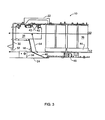
- FIG. 3 illustrates a cross-section of the electronic module 10 according to various embodiments.
- the electronic module 10 also includes a plurality of capacitors 36, a heat sink 38, a first switching device 40, a second switching device 42, one or more capacitor trays 44, a control board 46, and a deflector 48.
- the respective components of the electronic module 10 are positioned in a c manner which defines various paths for air flowing through the chassis 12. For reasons of clarity, the paths are shown in a single line format in FIG. 3 , and include a first path 50, a second path 52, and a third path 54.
- the capacitors 36 are positioned within the chassis 12, and at least one of the capacitors 36 is proximate the first end 14 of the chassis 12. According to various embodiments, the capacitors 36 are electrolytic capacitors.
- the heat sink 38 is positioned between the capacitors 36 and the bus bars 30.
- the heat sink 38 may be fabricated from any suitable thermally conductive material.
- the heat sink 38 is fabricated from a metal (e.g., lightweight aluminum) and incorporates a mechanically swagged hollow fin design. The fins are spaced apart from one another, and operate to dissipate heat and stop component debris from passing therebetween.
- the first switching device 40 is positioned between the heat sink 38 and the third side 22 of the chassis 12.
- the second switching device 42 is positioned between the heat sink 38 and the third side 22 of the chassis 12, as well as between the first switching device 40 and the second end 16 of the chassis 12.
- the first and second switching devices 40, 42 are implemented as insulated gate bipolar transistor modules and are configured to operate in parallel as one device.
- Each capacitor tray 44 is positioned within the chassis 12 between the capacitors 36 and the fourth side 24 of the chassis 12, and may be fabricated from any suitable material (e.g., a plastic).
- the capacitor tray 44 functions to help support the capacitors 36 in a position away from the fourth side 24 of the chassis 12.
- the capacitor tray also functions to stop at least a portion of component debris from passing therethrough.
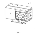
- a given capacitor tray 44 defines one or more openings 56 (see FIG. 4 ) aligned with corresponding capacitors 36, wherein each opening 56 is sized smaller than a circumference of the corresponding capacitor 36.
- the control board 46 is positioned between the capacitor tray 44 and the fourth side 24 of the chassis 12, includes a number of components, and is configured to monitor and/or control the operation of the electronic module 10.
- the control board 46 is configured to control the operation of first and second switching devices 40, 42, control fiber optic communications from the electronic module 10, etc.
- the portion of the fourth side 24 of the chassis 12 that the control board 46 is connected to may be hingedly connected to the chassis 12 to allow for easy access to the control board 46.
- the deflector 48 is positioned between the capacitors 36 and the second end 16 of the chassis 12, as well as between the heat sink 34 and the fourth side 24 of the chassis 12.
- the deflector 48 may be fabricated from any suitable material.
- the deflector is fabricated from a material (e.g., a metal, a plastic, etc.) having a thickness sufficient to stop at least some of the debris resulting from a failure of an internal component of the electronic module 10 from passing through the deflector 48.
- the deflector 48 is configured to redirect a portion of air approaching the deflector 48 toward the heat sink 38. Although the deflector 48 is shown in FIG.
- the functionality of the deflector 48 may be realized with other configurations.
- the deflector 48 defines an opening 58 therethrough.
- the opening 58 allows air flowing towards the deflector 48 to pass through the opening 58 toward the resistors 34.
- the opening 58 is aligned with the resistors 34.
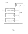
- FIG. 5 illustrates various embodiments of a system 60.
- the system 60 may be utilized in a variety of applications.
- the system 60 may be utilized as a power supply.
- the system 60 includes the electronic module 10 of FIG. 1 .
- the system 60 may include any number of electronic modules 10.
- the system 60 may include anywhere from one to twenty-four electronic modules 10. For purposes of clarity only three electronic modules 10 are shown in FIG. 5 .
- the system 60 also includes a fan 62.
- the fan 62 may be any type of fan suitable for moving air.
- the fan 62 is a backward inclined centrifugal fan.
- the fan 62 may be arranged in any suitable configuration with respect to the electronic modules 10.
- the fan 62 may be arranged in a draw-thru configuration as shown in FIG. 5 .
- the fan 62 may be arranged in a different configuration (e.g., blow-thru).
- the system 60 may include any number of fans 62.
- the system 60 includes two fans 62.
- one of the two fans 62 may be utilized as a redundant fan.
- the fan 62 serves to generate an airflow 64 through the respective electronic modules 10 of the system 60.
- a first portion of the airflow enters the chassis 12 at the one or more openings 28 defined by the first end 14 and proceeds along the first path 50.
- the airflow circulates around and comes in contact with the capacitors 36, thereby serving to cool the capacitors 36.
- the first portion of the airflow comes in contact with the heat sink 38 while circulating around and between the fins thereof, thereby serving to dissipate heat from the heat sink 38.
- the first portion of the airflow also sequentially comes in contact with the first switching device 40 and the second switching device 42, thereby serving to cool the switching devices 40, 42.
- the first portion of the airflow circulates around and comes in contact with the bus bars 30 and the power plug connectors 32 before exiting the second end 16 of the chassis 12, thereby serving to cool the bus bars 30 and the power plug connectors 32.
- a second portion of airflow enters the chassis 12 at the opening 26 defined by the first end 14 and proceeds along the second path 52.
- the airflow circulates around and comes in contact with the capacitor tray 44, and also comes in contact with portions of the capacitors 36 via the openings 56 defined by the capacitor tray 44, thereby serving to cool the capacitors 36 and the capacitor tray 44.
- the second portion of the airflow also circulates around and comes in contact with the control board 46, thereby serving to cool the control board 46.
- the second portion of the airflow After passing the volume occupied by the capacitor tray 44 and the control board 46, the second portion of the airflow approaches the deflector 48. A portion of the second portion of the airflow passes through the opening 58 defined by the deflector 48, then circulates around and comes in contact with the resistors 34, thereby serving to cool the resistors 34. After passing by the volume occupied by the resistors 34, the portion of the second portion of the airflow may also circulate around and come in contact with the bus bars 30 and the power plug connectors 32 before exiting at the second end 16 of the chassis 12, thereby serving to cool the bus bars 30 and the power plug connectors 32.
- the remaining portion of the second portion of the airflow comes near or in contact with the deflector 48, the remaining portion is deflected along the third path 54 toward the heat sink 38 and the second switching device 42.
- the remaining portion of the second portion of the airflow comes in contact with the heat sink 38 while circulating around and between the fins thereof, thereby serving to dissipate heat from the heat sink 38.
- the remaining portion of the second portion of the airflow also comes in contact with the second switching device 42, thereby serving to further cool the switching device 42.
- the additional cooling of the second switching device 42 by the remaining portion of the second portion of the airflow serves to maintain both of the switching devices 40, 42 at approximately the same temperature.
- the remaining portion of the second portion of the airflow effectively merges with the first portion of the airflow (i.e., the first and third paths 50, 54 combine with one another) and circulates around and comes in contact with the bus bars 30 and the power plug connectors 32 before exiting at the second end of the chassis 12.
- the above-described airflows and the configuration of the electronic module 10 also function to contain any failures which occur within the chassis 12.
- capacitors are known to overheat and fail in the absence of a sufficient amount of airflow. Some such failures result in the explosion of the capacitor.
- the chassis 12 is fabricated from a sufficient thickness of a suitably strong material (e.g., galvanized steel) and encloses substantially the entire electronic module 10, any of the debris resulting from such an explosion which comes in contact with the chassis 12 is not likely to pass through the chassis 12 (e.g., through one of the sides of the chassis).
- any debris resulting from the failure of other components within the chassis 12 of the electronic module 10 e.g., the control board, the switching devices, the resistors, etc.
- the construction of the chassis 12 operates to reduce the chance of the failure damaging any adjacent electronic modules 10.
- the capacitors 36 With the capacitors 36 positioned where they are the first components to come in contact with the first portion of the airflow, the capacitors 36 are exposed to the coolest air of the first portion of the airflow, thereby reducing the chance of overheating. Also, by having a portion of each capacitor exposed to the second portion of the airflow via the openings 56 in the capacitor tray 44, such capacitor portions are also exposed to the coolest air of the second portion of the airflow, thereby reducing the chance of overheating at the respective portions most likely to become overheated. In the event that one of the capacitors 36 does explode, the relatively high volume of airflow will carry the capacitor debris toward the heat sink 38, and the spaced-apart fins of the heat sink 38 will stop a significant portion of such debris from passing therebetween. Any debris which is not blocked by the heat sink 38 will be relatively small and cool, and may nonetheless be blocked from exiting the chassis 12 by the second end 16 of the chassis 12.
- control board 46 By also positioning the control board 46 to receive the coolest air of the second portion of the airflow, the potential for failure of the control board 46 is significantly reduced. In the event that one of the components of the control board 46 does explode, the relatively high volume of airflow will carry the capacitor debris toward the heat sink 38 via the deflector 48, where a significant portion of such debris will be blocked from advancing further. Any debris which is not blocked by the heat sink 38 may nonetheless be blocked from exiting the chassis 12 by the second end 16 of the chassis 12.
- first and second switching devices 40, 42 may be operated in parallel as a single device, it is advantageous to keep the two switching devices 40, 42 at approximately the same temperature.
- the first switching device 40 positioned before the second switching device 42 along the first airflow path 50, the heat transferred from the first switching device 40 to the first portion of airflow results in the second switching device 42 being exposed to somewhat warmer air from the first portion of airflow than the first switching device 40 is.
- the deflector 48 is positioned such that second switching device 42 is also exposed to the airflow from the third airflow path 54.
- the flow of air through the chassis 12 reduces the likelihood of such ionization occurring, thereby reducing the time of, and associated damage resulting from, an electric arc within the chassis 12.
Landscapes
- Engineering & Computer Science (AREA)
- Microelectronics & Electronic Packaging (AREA)
- Physics & Mathematics (AREA)
- Thermal Sciences (AREA)
- Cooling Or The Like Of Electrical Apparatus (AREA)
- Cooling Or The Like Of Semiconductors Or Solid State Devices (AREA)
Description
- This application discloses an invention that is related, generally and in various embodiments, to an electronic module configured for failure containment.
- Electronic modules come in a variety of shapes, sizes and configurations, and are utilized in a wide range of applications. For example, in some applications, the electronic modules form portions of a power supply, accept a three-phase AC input power, and output a single phase AC voltage. Such electronic modules include internal components which generate a measurable amount of heat, and such heat can affect the performance of the respective components and the electronic module itself.
- In many applications, the amount of heat generated causes certain components to fail. For example, it is known for capacitors to fail to due increased temperatures. Such failures can result in an explosion, and debris from the explosion can cause significant damage not only to the electronic module, but to other devices near the electronic module.
-
EP 0 356 991 discloses an electronic module having a chassis incorporating capacitors and a plurality of cooling fins positioned between the capacitors and a fist end of the chassis. The electronic module is configured to define at least one airflow path between the first and a second end of the chassis, the first and the second end being opposite to each other. - In one general respect, the present invention provides an electronic module as disclosed in claim 1.
- In another general respect, this application provides a system as disclosed in claim 15.
- Various embodiments of the invention are described herein by way of example in conjunction with the following figures.
-
FIG. 1 illustrates various embodiments of an electronic module; -
FIG. 2 illustrates various embodiments of the electronic module ofFIG. 1 ; -
FIG. 3 illustrates various embodiments of the electronic module ofFIG 1 ; -
FIG. 4 illustrates various embodiments of the electronic module ofFIG. 1 ; and -
FIG. 5 illustrates various embodiments of a system which includes the electronic module ofFIG. 1 . - It is to be understood that at least some of the figures and descriptions of the invention have been simplified to focus on elements that are relevant for a clear understanding of the invention, while eliminating, for purposes of clarity, other elements that those of ordinary skill in the art will appreciate may also comprise a portion of the invention. However, because such elements are well known in the art, and because they do not necessarily facilitate a better understanding of the invention, a description of such elements is not provided herein.
-
FIG. 1 andFIG. 2 illustrate various embodiments of anelectronic module 10. Theelectronic module 10 may be implemented as any type of module such as, for example, a power cell, a power supply, an inverter, a drive chassis, etc. According to various embodiments, theelectronic module 10 is implemented as a power cell which accepts three phase AC input power and outputs a single phase AC voltage. Such a power cell is described inU.S. Patent 5,625,545 (Hammond ), and includes an AC-to-DC rectifier, a smoothing circuit, an output DC-to-AC converter, and a control circuit. - The
electronic module 10 includes achassis 12 having afirst end 14 and asecond end 16 which is opposite thefirst end 14. Thefirst end 14 may be considered the "front" of theelectronic module 10. Thesecond end 16 is opposite thefirst end 14 and may be considered the "back" of theelectronic module 10. According to various embodiments, thechassis 12 may be comprised of several portions connected together (e.g., a top, a bottom, and four sides), and one or more portions of thechassis 12 may be removable. Thechassis 12 defines an exterior portion of theelectronic module 10, and encloses various components (e.g., any or all of the following: capacitors, printed circuit boards, heat sink, switching devices, resistors, etc.) of theelectronic module 10. Thechassis 12 may be fabricated from any suitable material. For example, according to various embodiments, thechassis 12 is fabricated from a conductive material such as a metal (e.g., galvanized steel). For such embodiments, the conductive material of thechassis 12 may serve to provide a low impedance path for arcing faults within thechassis 12 to minimize potential damage caused thereby. Thechassis 12 may be of a thickness sufficient to stop any debris resulting from a failure of an internal component of theelectronic module 10 from exiting the space enclosed by thechassis 12, thereby preventing any collateral damage to other components in the vicinity of theelectronic module 10. In addition, thechassis 12 may serve to protect internal components of theelectronic module 10 from damage during shipping and handling, and may be configured in a manner such that theelectronic module 10 can be placed on any of its sides without causing any damage to the components of theelectronic module 10. Furthermore, as described in more detail hereinbelow, thechassis 12 may also define an air plenum utilized to assist in the forced air cooling of all components within thechassis 12. - The
chassis 12 also includes afirst side 18, asecond side 20, a third side 22 (seeFIG. 3 ), and afourth side 24. Thefirst side 18 may be considered the "right" side of thechassis 12. Thesecond side 20 is opposite thefirst side 18, and may be considered the "left" side of thechassis 12. Thethird side 22 is connected to at least one of the first andsecond sides chassis 12. For purposes of clarity, theelectronic module 10 is shown having thethird side 22 removed inFIG. 1 andFIG. 2 . Thefourth side 24 is opposite thethird side 22, is connected to at least one of the first andsecond sides chassis 12. The sides of the chassis are fabricated from a material (e.g., galvanized steel) which stops component debris from passing therethrough. As shown inFIG. 1 , thefirst end 14 defines anopening 26 proximate thefourth side 24, and also defines one ormore openings 28 proximate theopening 26. Collectively, the first and second ends 14,16, and the first, second, third, andfourth sides chassis 12 enclose substantially the entireelectronic module 10. - As shown in
FIG. 2 , theelectronic module 10 includes a plurality ofbus bars 30 positioned within thechassis 12 proximate thesecond end 16, a plurality ofpower plug connectors 32 positioned proximate thesecond end 16, and a plurality ofresistors 34 positioned proximate thesecond end 16. Theresistors 34 are electrically connected to capacitors of theelectronic module 10, and function to bleed current from the capacitors when power to theelectronic module 10 is interrupted or shut down. - The bus bars 30 may be fabricated from any suitable conductive material, and are collectively configured to route power to and from the
electronic module 10. For this embodiment, at least two of the bus bars 30 are configured as input bus bars and at least two of the bus bars 30 are configured as output bus bars. The number, size and shape of the bus bars 30 can vary by application. In general, the respective bus bars 30 are sized to accommodate requirements associated with a particular application. - According to various embodiments, each
power plug connector 32 includes a conductive material and a housing which surrounds the conductive material. The conductive material may be fabricated from any suitable conductor such as, for example, copper. The housing may be fabricated from any suitable insulating material such as, for example, a plastic. The housing defines an opening configured to receive a portion of a system bus when theelectronic module 10 is connected to a system bus. The opening surrounds the conductive material, and the conductive material defines a smaller opening configured to receive the portion of the system bus when theelectronic module 10 is connected to the system bus. Thus, the housing and the conductive material collectively define an opening which is sized to receive the portion of the system bus when theelectronic module 10 is connected to the system bus. - As shown in
FIG. 2 , thepower plug connectors 32 are connected to corresponding bus bars 30. A givenpower plug connector 32 may be connected to acorresponding bus bar 30 in any suitable manner. For example, according to various embodiments, thepower plug connector 32 is mechanically connected to thebus bar 30 via fasteners (e.g., screws or nuts and bolts) in a manner that places the conductive material in direct contact with thebus bar 30. Thus, thebus bar 30 may also act as a heat sink for thepower plug connector 32 connected thereto. Thepower plug connector 32 is configured such that it can be connected to thebus bar 30 in a manner that the permits some movement of thepower plug connector 32. - According to other embodiments, the power plug connectors may be configured in a different manner. For example, according to various embodiments, a given power plug connector may include a male portion and a separate female portion which collectively function to connect the
electronic module 10 to the system bus. For some embodiments, the male portion is connected to the corresponding bus bar and the female portion is connected to the system bus. In other embodiments, the male portion is connected to system bus and the female portion is connected to the corresponding bus bar. In general, for a given application, the particular configuration of power plug connectors are selected to accommodate requirements associated with a particular application. -
FIG. 3 illustrates a cross-section of theelectronic module 10 according to various embodiments. As shown inFIG. 3 , theelectronic module 10 also includes a plurality ofcapacitors 36, aheat sink 38, afirst switching device 40, asecond switching device 42, one ormore capacitor trays 44, acontrol board 46, and adeflector 48. As explained in more detail hereinbelow, the respective components of theelectronic module 10 are positioned in a c manner which defines various paths for air flowing through thechassis 12. For reasons of clarity, the paths are shown in a single line format inFIG. 3 , and include a first path 50, asecond path 52, and athird path 54. - The
capacitors 36 are positioned within thechassis 12, and at least one of thecapacitors 36 is proximate thefirst end 14 of thechassis 12. According to various embodiments, thecapacitors 36 are electrolytic capacitors. Theheat sink 38 is positioned between thecapacitors 36 and the bus bars 30. Theheat sink 38 may be fabricated from any suitable thermally conductive material. For example, according to various embodiments, theheat sink 38 is fabricated from a metal (e.g., lightweight aluminum) and incorporates a mechanically swagged hollow fin design. The fins are spaced apart from one another, and operate to dissipate heat and stop component debris from passing therebetween. Thefirst switching device 40 is positioned between theheat sink 38 and thethird side 22 of thechassis 12. Thesecond switching device 42 is positioned between theheat sink 38 and thethird side 22 of thechassis 12, as well as between thefirst switching device 40 and thesecond end 16 of thechassis 12. According to various embodiments, the first andsecond switching devices - Each
capacitor tray 44 is positioned within thechassis 12 between thecapacitors 36 and thefourth side 24 of thechassis 12, and may be fabricated from any suitable material (e.g., a plastic). Thecapacitor tray 44 functions to help support thecapacitors 36 in a position away from thefourth side 24 of thechassis 12. The capacitor tray also functions to stop at least a portion of component debris from passing therethrough. According to various embodiments, a givencapacitor tray 44 defines one or more openings 56 (seeFIG. 4 ) aligned withcorresponding capacitors 36, wherein eachopening 56 is sized smaller than a circumference of the correspondingcapacitor 36. - The
control board 46 is positioned between thecapacitor tray 44 and thefourth side 24 of thechassis 12, includes a number of components, and is configured to monitor and/or control the operation of theelectronic module 10. For example, according to various embodiments, thecontrol board 46 is configured to control the operation of first andsecond switching devices electronic module 10, etc. As shown inFIG. 4 , according to various embodiments, the portion of thefourth side 24 of thechassis 12 that thecontrol board 46 is connected to may be hingedly connected to thechassis 12 to allow for easy access to thecontrol board 46. - Returning to
FIG. 3 , thedeflector 48 is positioned between thecapacitors 36 and thesecond end 16 of thechassis 12, as well as between theheat sink 34 and thefourth side 24 of thechassis 12. Thedeflector 48 may be fabricated from any suitable material. According to various embodiments, the deflector is fabricated from a material (e.g., a metal, a plastic, etc.) having a thickness sufficient to stop at least some of the debris resulting from a failure of an internal component of theelectronic module 10 from passing through thedeflector 48. Thedeflector 48 is configured to redirect a portion of air approaching thedeflector 48 toward theheat sink 38. Although thedeflector 48 is shown inFIG. 3 as having a distinct bend, the functionality of thedeflector 48 may be realized with other configurations. As shown inFIG. 3 , thedeflector 48 defines anopening 58 therethrough. Theopening 58 allows air flowing towards thedeflector 48 to pass through theopening 58 toward theresistors 34. According to various embodiments, theopening 58 is aligned with theresistors 34. -
FIG. 5 illustrates various embodiments of asystem 60. Thesystem 60 may be utilized in a variety of applications. For example, thesystem 60 may be utilized as a power supply. Thesystem 60 includes theelectronic module 10 ofFIG. 1 . According to various embodiments, thesystem 60 may include any number ofelectronic modules 10. For example, according to various embodiments, thesystem 60 may include anywhere from one to twenty-fourelectronic modules 10. For purposes of clarity only threeelectronic modules 10 are shown inFIG. 5 . - The
system 60 also includes afan 62. Thefan 62 may be any type of fan suitable for moving air. For example, according to various embodiments, thefan 62 is a backward inclined centrifugal fan. Additionally, thefan 62 may be arranged in any suitable configuration with respect to theelectronic modules 10. For example, thefan 62 may be arranged in a draw-thru configuration as shown inFIG. 5 . According to other embodiments, thefan 62 may be arranged in a different configuration (e.g., blow-thru). Thesystem 60 may include any number offans 62. For example, according to various embodiments, thesystem 60 includes twofans 62. For such embodiments, one of the twofans 62 may be utilized as a redundant fan. - In operation, the
fan 62 serves to generate anairflow 64 through the respectiveelectronic modules 10 of thesystem 60. A first portion of the airflow enters thechassis 12 at the one ormore openings 28 defined by thefirst end 14 and proceeds along the first path 50. As the first portion of the airflow advances along the first path 50 toward thesecond end 16, the airflow circulates around and comes in contact with thecapacitors 36, thereby serving to cool thecapacitors 36. After passing the volume proximate thecapacitors 36, the first portion of the airflow comes in contact with theheat sink 38 while circulating around and between the fins thereof, thereby serving to dissipate heat from theheat sink 38. Concurrent therewith, the first portion of the airflow also sequentially comes in contact with thefirst switching device 40 and thesecond switching device 42, thereby serving to cool theswitching devices heat sink 38 and the first andsecond switching devices power plug connectors 32 before exiting thesecond end 16 of thechassis 12, thereby serving to cool the bus bars 30 and thepower plug connectors 32. - Concurrent with the flow of the first portion of the airflow through the
chassis 12, a second portion of airflow enters thechassis 12 at theopening 26 defined by thefirst end 14 and proceeds along thesecond path 52. As the second portion of the airflow advances along thesecond path 52 toward thesecond end 16, the airflow circulates around and comes in contact with thecapacitor tray 44, and also comes in contact with portions of thecapacitors 36 via theopenings 56 defined by thecapacitor tray 44, thereby serving to cool thecapacitors 36 and thecapacitor tray 44. Concurrent therewith, the second portion of the airflow also circulates around and comes in contact with thecontrol board 46, thereby serving to cool thecontrol board 46. - After passing the volume occupied by the
capacitor tray 44 and thecontrol board 46, the second portion of the airflow approaches thedeflector 48. A portion of the second portion of the airflow passes through theopening 58 defined by thedeflector 48, then circulates around and comes in contact with theresistors 34, thereby serving to cool theresistors 34. After passing by the volume occupied by theresistors 34, the portion of the second portion of the airflow may also circulate around and come in contact with the bus bars 30 and thepower plug connectors 32 before exiting at thesecond end 16 of thechassis 12, thereby serving to cool the bus bars 30 and thepower plug connectors 32. - When the remaining portion of the second portion of the airflow comes near or in contact with the
deflector 48, the remaining portion is deflected along thethird path 54 toward theheat sink 38 and thesecond switching device 42. The remaining portion of the second portion of the airflow comes in contact with theheat sink 38 while circulating around and between the fins thereof, thereby serving to dissipate heat from theheat sink 38. The remaining portion of the second portion of the airflow also comes in contact with thesecond switching device 42, thereby serving to further cool theswitching device 42. The additional cooling of thesecond switching device 42 by the remaining portion of the second portion of the airflow serves to maintain both of theswitching devices third paths 50, 54 combine with one another) and circulates around and comes in contact with the bus bars 30 and thepower plug connectors 32 before exiting at the second end of thechassis 12. - The above-described airflows and the configuration of the
electronic module 10 also function to contain any failures which occur within thechassis 12. In general, capacitors are known to overheat and fail in the absence of a sufficient amount of airflow. Some such failures result in the explosion of the capacitor. As thechassis 12 is fabricated from a sufficient thickness of a suitably strong material (e.g., galvanized steel) and encloses substantially the entireelectronic module 10, any of the debris resulting from such an explosion which comes in contact with thechassis 12 is not likely to pass through the chassis 12 (e.g., through one of the sides of the chassis). Similarly, any debris resulting from the failure of other components within thechassis 12 of the electronic module 10 (e.g., the control board, the switching devices, the resistors, etc.) which comes in contact with thechassis 12 also is not likely to pass through thechassis 12. Thus, when a failure occurs in a givenelectronic module 10, the construction of thechassis 12 operates to reduce the chance of the failure damaging any adjacentelectronic modules 10. - With the
capacitors 36 positioned where they are the first components to come in contact with the first portion of the airflow, thecapacitors 36 are exposed to the coolest air of the first portion of the airflow, thereby reducing the chance of overheating. Also, by having a portion of each capacitor exposed to the second portion of the airflow via theopenings 56 in thecapacitor tray 44, such capacitor portions are also exposed to the coolest air of the second portion of the airflow, thereby reducing the chance of overheating at the respective portions most likely to become overheated. In the event that one of thecapacitors 36 does explode, the relatively high volume of airflow will carry the capacitor debris toward theheat sink 38, and the spaced-apart fins of theheat sink 38 will stop a significant portion of such debris from passing therebetween. Any debris which is not blocked by theheat sink 38 will be relatively small and cool, and may nonetheless be blocked from exiting thechassis 12 by thesecond end 16 of thechassis 12. - By also positioning the
control board 46 to receive the coolest air of the second portion of the airflow, the potential for failure of thecontrol board 46 is significantly reduced. In the event that one of the components of thecontrol board 46 does explode, the relatively high volume of airflow will carry the capacitor debris toward theheat sink 38 via thedeflector 48, where a significant portion of such debris will be blocked from advancing further. Any debris which is not blocked by theheat sink 38 may nonetheless be blocked from exiting thechassis 12 by thesecond end 16 of thechassis 12. - As the first and
second switching devices switching devices first switching device 40 positioned before thesecond switching device 42 along the first airflow path 50, the heat transferred from thefirst switching device 40 to the first portion of airflow results in thesecond switching device 42 being exposed to somewhat warmer air from the first portion of airflow than thefirst switching device 40 is. To promote similar cooling of the first andsecond switching devices deflector 48 is positioned such thatsecond switching device 42 is also exposed to the airflow from thethird airflow path 54. - As air within the
chassis 12 may become ionized, the flow of air through thechassis 12 reduces the likelihood of such ionization occurring, thereby reducing the time of, and associated damage resulting from, an electric arc within thechassis 12. - While several embodiments of the invention have been described herein by way of example, those skilled in the art will appreciate that various modifications, alterations, and adaptions to the described embodiments may be realized without departing from the scope of the invention defined by the appended claims.
Claims (15)
- An electronic module (10), comprising:a chassis (12) having a first end (14) and a second end (16) opposite the first end (14), wherein the chassis (12) comprises:a first side (18);a second side (20) opposite the first side (18);a third side (22) connected to at least one of the first and second sides (18, 20); anda fourth side (24) connected to at least one of the first (18) and second sides (20) wherein the fourth side (24) is opposite the third side (22);a plurality of capacitors (36) positioned within the chassis (12); anda heat sink (38) positioned between the capacitors (36) and the second end (16);wherein the electronic module is configured to define at least one path (50, 52, 54) between the first end (14) and the second end (16) for air flowing through the chassis (12), such that debris resulting from a failure of one of the plurality of capacitors (36) may be carried by air flowing through the chassis (12) toward the heat sink (38), the heat sink being configured to block a significant portion of such debris, and the second end (16) being configured to block debris which is not blocked by the heat sink (38), andwherein the chassis (12) is fabricated from a material which stops debris resulting from a failure of one of the plurality of capacitors (36) from passing through the sides of the chassis.
- The electronic module of claim 1, wherein the material is a metal.
- The electronic module of claim 2, wherein the metal is galvanized steel.
- The electronic module of claim 1, wherein a portion of one of the sides is hingedly connected to the chassis (12).
- The electronic module of claim 1, wherein at least one of the capacitors (36) is an electrolytic capacitor.
- The electronic module of claim 1, wherein the heat sink (38) is fabricated from a thermally conductive material.
- The electronic module of claim 6, wherein the thermally conductive material is aluminum.
- The electronic module of claim 1, wherein the heat sink (38) comprises spaced- apart fins which stop at least some of the component debris from passing therebetween.
- The electronic module of claim 1, further comprising a capacitor tray (44) positioned between the capacitors (36) and one of the sides (18, 20, 22, 24) of the chassis (12), wherein the capacitor tray (44) is fabricated from a material which stops at least some debris resulting from a failure of one of the plurality of capacitors (36) from passing therethrough.
- The electronic module of claim 9, further comprising a control board (46) positioned between the capacitor tray (44) and one of the sides of the chassis (12).
- The electronic module of claim 1, further comprising a deflector (48) positioned between the capacitors (36) and the second end (16), wherein the deflector (48) is fabricated from a material which stops at least some debris resulting from a failure of one of the plurality of capacitors (36) from passing therethrough.
- The electronic module of claim 1, further comprising a first switching device (40) positioned between the heat sink (38) and one of the sides of the chassis (12).
- The electronic module of claim 12, further comprising a second switching device (42) positioned between the heat sink (38) and the one of the sides of the chassis (12).
- The electronic module of claim 1, further comprising a resistor (34) positioned between the deflector (48) and the second end (16).
- A system, comprising:an electronic module according to any one of the preceding claims, and wherein the electronic module comprises:a fan configured to generate said airflow through the electronic module along said at least one path (50, 52, 54).
Applications Claiming Priority (3)
| Application Number | Priority Date | Filing Date | Title |
|---|---|---|---|
| US81808106P | 2006-06-30 | 2006-06-30 | |
| US11/769,891 US7869211B2 (en) | 2006-06-30 | 2007-06-28 | Electronic module configured for failure containment and system including same |
| PCT/US2007/015201 WO2008005374A2 (en) | 2006-06-30 | 2007-06-29 | Electronic module configured for failure containment and system including same |
Publications (3)
| Publication Number | Publication Date |
|---|---|
| EP2036418A2 EP2036418A2 (en) | 2009-03-18 |
| EP2036418B1 true EP2036418B1 (en) | 2015-04-29 |
| EP2036418B8 EP2036418B8 (en) | 2015-06-10 |
Family
ID=38895155
Family Applications (1)
| Application Number | Title | Priority Date | Filing Date |
|---|---|---|---|
| EP07810079.9A Not-in-force EP2036418B8 (en) | 2006-06-30 | 2007-06-29 | Electronic module configured for failure containment and system including same |
Country Status (8)
| Country | Link |
|---|---|
| US (1) | US7869211B2 (en) |
| EP (1) | EP2036418B8 (en) |
| JP (1) | JP5279706B2 (en) |
| CN (1) | CN101491168B (en) |
| BR (1) | BRPI0713949B1 (en) |
| CA (1) | CA2656201C (en) |
| MX (1) | MX2009000041A (en) |
| WO (1) | WO2008005374A2 (en) |
Families Citing this family (6)
| Publication number | Priority date | Publication date | Assignee | Title |
|---|---|---|---|---|
| USD702670S1 (en) * | 2009-03-26 | 2014-04-15 | Tait Towers Manufacturing, LLC | Video screen frame |
| ES2375332T3 (en) * | 2009-09-18 | 2012-02-28 | Sma Solar Technology Ag | INVESTOR WITH A HOUSING. |
| US20110140686A1 (en) * | 2009-12-16 | 2011-06-16 | Lineage Power Corporation | Thermal extension structures for monitoring bus bar terminations |
| FR2973640B1 (en) * | 2011-04-04 | 2013-04-05 | Schneider Toshiba Inverter Europe Sas | SPEED DRIVE WITH OPTIMIZED ARCHITECTURE |
| USD676029S1 (en) | 2012-06-15 | 2013-02-12 | Peerless Industries, Inc. | System for mounting audio/visual devices or the like from an overhead structure |
| US10483251B1 (en) | 2018-11-09 | 2019-11-19 | Chongqing Jinkang New Energy Vehicle Co., Ltd. | Power module for drivetrain of an electric vehicle |
Family Cites Families (29)
| Publication number | Priority date | Publication date | Assignee | Title |
|---|---|---|---|---|
| US3415583A (en) * | 1966-07-18 | 1968-12-10 | Myron J. Zucker | Capacitor mounting case |
| US4027206A (en) * | 1975-01-27 | 1977-05-31 | L. H. Research | Electronic cooling chassis |
| KR920005988B1 (en) | 1988-08-31 | 1992-07-25 | 가부시기가이샤 히다찌세이사꾸쇼 | Inverter |
| JPH0484496A (en) * | 1990-07-27 | 1992-03-17 | Nippon Light Metal Co Ltd | Housing for electronic equipment |
| US5335143A (en) * | 1993-08-05 | 1994-08-02 | International Business Machines Corporation | Disk augmented heat transfer system |
| US5625545A (en) * | 1994-03-01 | 1997-04-29 | Halmar Robicon Group | Medium voltage PWM drive and method |
| US5680294A (en) * | 1995-03-28 | 1997-10-21 | The Whitaker Corporation | Pluggable power supply for card cage |
| JPH099409A (en) * | 1995-06-21 | 1997-01-10 | Toshiba Corp | Vehicle power converter unit |
| US5648892A (en) * | 1995-09-29 | 1997-07-15 | Allen-Bradley Company, Inc. | Wireless circuit board system for a motor controller |
| US6046921A (en) * | 1996-08-27 | 2000-04-04 | Tracewell; Larry L. | Modular power supply |
| US5831847A (en) * | 1997-02-05 | 1998-11-03 | Jerome Industries Corp. | Power supply with separated airflows |
| JP3237609B2 (en) * | 1998-05-11 | 2001-12-10 | 株式会社日立製作所 | Inverter device |
| JP3569451B2 (en) * | 1998-09-07 | 2004-09-22 | 株式会社Pfu | Electronic equipment with heat dissipation device |
| US6081423A (en) * | 1998-12-22 | 2000-06-27 | The Esab Group, Inc. | Power supply with obliquely impinging airflow |
| JP4388174B2 (en) * | 1999-09-06 | 2009-12-24 | 株式会社ソニー・コンピュータエンタテインメント | Electronics |
| JP2001168240A (en) * | 1999-10-08 | 2001-06-22 | Trw Inc | Integrated microelectronics module |
| JP3814475B2 (en) * | 2000-09-26 | 2006-08-30 | 株式会社日立国際電気 | amplifier |
| DE10143547B4 (en) | 2001-09-06 | 2005-03-10 | Rexroth Indramat Gmbh | Active outdoor-cooled housing with at least one heat dissipation-generating electronic component |
| US6889752B2 (en) * | 2002-07-11 | 2005-05-10 | Avaya Technology Corp. | Systems and methods for weatherproof cabinets with multiple compartment cooling |
| JP4360123B2 (en) * | 2003-05-27 | 2009-11-11 | 三菱電機株式会社 | Power converter |
| TWI260484B (en) * | 2003-08-12 | 2006-08-21 | Asustek Comp Inc | Heat sink for power device on computer motherboard |
| US7019996B2 (en) * | 2003-10-16 | 2006-03-28 | Ballard Power Systems Corporation | Power converter employing a planar transformer |
| JP4207755B2 (en) * | 2003-11-07 | 2009-01-14 | 株式会社豊田自動織機 | Electronic equipment |
| US7313000B2 (en) * | 2003-12-05 | 2007-12-25 | Ultra Products, Inc. | Power distribution system for a personal computer |
| JP2005348533A (en) * | 2004-06-03 | 2005-12-15 | Fuji Electric Fa Components & Systems Co Ltd | Inverter device |
| JP4411147B2 (en) * | 2004-06-24 | 2010-02-10 | 株式会社日立製作所 | Heat sink with fan |
| US7595976B2 (en) * | 2004-10-21 | 2009-09-29 | Mitsubishi Denki Kabushiki Kaisha | Outdoor apparatus |
| TWI259522B (en) * | 2005-08-02 | 2006-08-01 | Quanta Comp Inc | Electronic device |
| US7554804B2 (en) * | 2006-06-30 | 2009-06-30 | Siemens Energy & Automation, Inc. | Electronic module configured for air flow therethrough and system including same |
-
2007
- 2007-06-28 US US11/769,891 patent/US7869211B2/en active Active
- 2007-06-29 JP JP2009518308A patent/JP5279706B2/en not_active Expired - Fee Related
- 2007-06-29 MX MX2009000041A patent/MX2009000041A/en active IP Right Grant
- 2007-06-29 CN CN2007800248768A patent/CN101491168B/en active Active
- 2007-06-29 EP EP07810079.9A patent/EP2036418B8/en not_active Not-in-force
- 2007-06-29 CA CA2656201A patent/CA2656201C/en active Active
- 2007-06-29 WO PCT/US2007/015201 patent/WO2008005374A2/en not_active Ceased
- 2007-06-29 BR BRPI0713949A patent/BRPI0713949B1/en not_active IP Right Cessation
Also Published As
| Publication number | Publication date |
|---|---|
| WO2008005374A2 (en) | 2008-01-10 |
| JP5279706B2 (en) | 2013-09-04 |
| BRPI0713949B1 (en) | 2019-01-02 |
| US20090016018A1 (en) | 2009-01-15 |
| MX2009000041A (en) | 2009-03-06 |
| CN101491168A (en) | 2009-07-22 |
| US7869211B2 (en) | 2011-01-11 |
| CA2656201C (en) | 2015-03-24 |
| CA2656201A1 (en) | 2008-01-10 |
| JP2009543343A (en) | 2009-12-03 |
| EP2036418A2 (en) | 2009-03-18 |
| BRPI0713949A2 (en) | 2012-12-04 |
| BRPI0713949A8 (en) | 2017-03-07 |
| WO2008005374A3 (en) | 2008-09-18 |
| CN101491168B (en) | 2011-08-24 |
| EP2036418B8 (en) | 2015-06-10 |
Similar Documents
| Publication | Publication Date | Title |
|---|---|---|
| EP2036417B1 (en) | Electronic module configured for air flow therethrough and system including same | |
| US10622790B2 (en) | Arc ventilation system of multi stage distributing board | |
| CA2656201C (en) | Electronic module configured for failure containment and system including same | |
| US9398682B2 (en) | Devices and methods for cooling components on a PCB | |
| EP2642841B1 (en) | Electronic device | |
| EP1920527B1 (en) | Packaging system for modular power cells | |
| EP1077488A2 (en) | Thermally efficient motor controller assembly | |
| US9906154B2 (en) | Power conversion unit and power conversion device | |
| US20070048561A1 (en) | Packaging method for modular power cells | |
| EP3001550B1 (en) | Power module for medium and high-voltage frequency converter and frequency converter comprising same | |
| US10128639B1 (en) | High current busbar system for low-profile power shelves | |
| RU2474986C1 (en) | Modular electric circuit board for power components | |
| CN207398926U (en) | A kind of UPS complete machines | |
| US20180006573A1 (en) | Electrical Power Conversion Unit and Electrical Power Conversion Device | |
| US20210168926A1 (en) | Backplane and method for producing same |
Legal Events
| Date | Code | Title | Description |
|---|---|---|---|
| PUAI | Public reference made under article 153(3) epc to a published international application that has entered the european phase |
Free format text: ORIGINAL CODE: 0009012 |
|
| 17P | Request for examination filed |
Effective date: 20081222 |
|
| AK | Designated contracting states |
Kind code of ref document: A2 Designated state(s): AT BE BG CH CY CZ DE DK EE ES FI FR GB GR HU IE IS IT LI LT LU LV MC MT NL PL PT RO SE SI SK TR |
|
| AX | Request for extension of the european patent |
Extension state: AL BA HR MK RS |
|
| DAX | Request for extension of the european patent (deleted) | ||
| RAP1 | Party data changed (applicant data changed or rights of an application transferred) |
Owner name: SIEMENS INDUSTRY, INC. |
|
| GRAP | Despatch of communication of intention to grant a patent |
Free format text: ORIGINAL CODE: EPIDOSNIGR1 |
|
| INTG | Intention to grant announced |
Effective date: 20141120 |
|
| GRAS | Grant fee paid |
Free format text: ORIGINAL CODE: EPIDOSNIGR3 |
|
| GRAA | (expected) grant |
Free format text: ORIGINAL CODE: 0009210 |
|
| AK | Designated contracting states |
Kind code of ref document: B1 Designated state(s): AT BE BG CH CY CZ DE DK EE ES FI FR GB GR HU IE IS IT LI LT LU LV MC MT NL PL PT RO SE SI SK TR |
|
| REG | Reference to a national code |
Ref country code: GB Ref legal event code: FG4D |
|
| REG | Reference to a national code |
Ref country code: CH Ref legal event code: EP |
|
| REG | Reference to a national code |
Ref country code: AT Ref legal event code: REF Ref document number: 725043 Country of ref document: AT Kind code of ref document: T Effective date: 20150515 |
|
| RAP2 | Party data changed (patent owner data changed or rights of a patent transferred) |
Owner name: SIEMENS AKTIENGESELLSCHAFT |
|
| REG | Reference to a national code |
Ref country code: IE Ref legal event code: FG4D |
|
| REG | Reference to a national code |
Ref country code: DE Ref legal event code: R096 Ref document number: 602007041260 Country of ref document: DE Effective date: 20150611 |
|
| REG | Reference to a national code |
Ref country code: CH Ref legal event code: NV Representative=s name: SIEMENS SCHWEIZ AG, CH |
|
| REG | Reference to a national code |
Ref country code: NL Ref legal event code: VDEP Effective date: 20150429 |
|
| REG | Reference to a national code |
Ref country code: AT Ref legal event code: MK05 Ref document number: 725043 Country of ref document: AT Kind code of ref document: T Effective date: 20150429 |
|
| REG | Reference to a national code |
Ref country code: LT Ref legal event code: MG4D |
|
| PG25 | Lapsed in a contracting state [announced via postgrant information from national office to epo] |
Ref country code: NL Free format text: LAPSE BECAUSE OF FAILURE TO SUBMIT A TRANSLATION OF THE DESCRIPTION OR TO PAY THE FEE WITHIN THE PRESCRIBED TIME-LIMIT Effective date: 20150429 |
|
| PG25 | Lapsed in a contracting state [announced via postgrant information from national office to epo] |
Ref country code: LT Free format text: LAPSE BECAUSE OF FAILURE TO SUBMIT A TRANSLATION OF THE DESCRIPTION OR TO PAY THE FEE WITHIN THE PRESCRIBED TIME-LIMIT Effective date: 20150429 Ref country code: PT Free format text: LAPSE BECAUSE OF FAILURE TO SUBMIT A TRANSLATION OF THE DESCRIPTION OR TO PAY THE FEE WITHIN THE PRESCRIBED TIME-LIMIT Effective date: 20150831 Ref country code: FI Free format text: LAPSE BECAUSE OF FAILURE TO SUBMIT A TRANSLATION OF THE DESCRIPTION OR TO PAY THE FEE WITHIN THE PRESCRIBED TIME-LIMIT Effective date: 20150429 Ref country code: ES Free format text: LAPSE BECAUSE OF FAILURE TO SUBMIT A TRANSLATION OF THE DESCRIPTION OR TO PAY THE FEE WITHIN THE PRESCRIBED TIME-LIMIT Effective date: 20150429 |
|
| PG25 | Lapsed in a contracting state [announced via postgrant information from national office to epo] |
Ref country code: IS Free format text: LAPSE BECAUSE OF FAILURE TO SUBMIT A TRANSLATION OF THE DESCRIPTION OR TO PAY THE FEE WITHIN THE PRESCRIBED TIME-LIMIT Effective date: 20150829 Ref country code: LV Free format text: LAPSE BECAUSE OF FAILURE TO SUBMIT A TRANSLATION OF THE DESCRIPTION OR TO PAY THE FEE WITHIN THE PRESCRIBED TIME-LIMIT Effective date: 20150429 Ref country code: GR Free format text: LAPSE BECAUSE OF FAILURE TO SUBMIT A TRANSLATION OF THE DESCRIPTION OR TO PAY THE FEE WITHIN THE PRESCRIBED TIME-LIMIT Effective date: 20150730 Ref country code: AT Free format text: LAPSE BECAUSE OF FAILURE TO SUBMIT A TRANSLATION OF THE DESCRIPTION OR TO PAY THE FEE WITHIN THE PRESCRIBED TIME-LIMIT Effective date: 20150429 |
|
| PG25 | Lapsed in a contracting state [announced via postgrant information from national office to epo] |
Ref country code: DK Free format text: LAPSE BECAUSE OF FAILURE TO SUBMIT A TRANSLATION OF THE DESCRIPTION OR TO PAY THE FEE WITHIN THE PRESCRIBED TIME-LIMIT Effective date: 20150429 Ref country code: EE Free format text: LAPSE BECAUSE OF FAILURE TO SUBMIT A TRANSLATION OF THE DESCRIPTION OR TO PAY THE FEE WITHIN THE PRESCRIBED TIME-LIMIT Effective date: 20150429 Ref country code: IT Free format text: LAPSE BECAUSE OF FAILURE TO SUBMIT A TRANSLATION OF THE DESCRIPTION OR TO PAY THE FEE WITHIN THE PRESCRIBED TIME-LIMIT Effective date: 20150429 Ref country code: MC Free format text: LAPSE BECAUSE OF FAILURE TO SUBMIT A TRANSLATION OF THE DESCRIPTION OR TO PAY THE FEE WITHIN THE PRESCRIBED TIME-LIMIT Effective date: 20150429 |
|
| REG | Reference to a national code |
Ref country code: DE Ref legal event code: R097 Ref document number: 602007041260 Country of ref document: DE |
|
| PG25 | Lapsed in a contracting state [announced via postgrant information from national office to epo] |
Ref country code: PL Free format text: LAPSE BECAUSE OF FAILURE TO SUBMIT A TRANSLATION OF THE DESCRIPTION OR TO PAY THE FEE WITHIN THE PRESCRIBED TIME-LIMIT Effective date: 20150429 Ref country code: RO Free format text: LAPSE BECAUSE OF NON-PAYMENT OF DUE FEES Effective date: 20150429 Ref country code: LU Free format text: LAPSE BECAUSE OF FAILURE TO SUBMIT A TRANSLATION OF THE DESCRIPTION OR TO PAY THE FEE WITHIN THE PRESCRIBED TIME-LIMIT Effective date: 20150629 Ref country code: SK Free format text: LAPSE BECAUSE OF FAILURE TO SUBMIT A TRANSLATION OF THE DESCRIPTION OR TO PAY THE FEE WITHIN THE PRESCRIBED TIME-LIMIT Effective date: 20150429 Ref country code: CZ Free format text: LAPSE BECAUSE OF FAILURE TO SUBMIT A TRANSLATION OF THE DESCRIPTION OR TO PAY THE FEE WITHIN THE PRESCRIBED TIME-LIMIT Effective date: 20150429 |
|
| PLBE | No opposition filed within time limit |
Free format text: ORIGINAL CODE: 0009261 |
|
| STAA | Information on the status of an ep patent application or granted ep patent |
Free format text: STATUS: NO OPPOSITION FILED WITHIN TIME LIMIT |
|
| REG | Reference to a national code |
Ref country code: IE Ref legal event code: MM4A |
|
| 26N | No opposition filed |
Effective date: 20160201 |
|
| PG25 | Lapsed in a contracting state [announced via postgrant information from national office to epo] |
Ref country code: IE Free format text: LAPSE BECAUSE OF NON-PAYMENT OF DUE FEES Effective date: 20150629 |
|
| PG25 | Lapsed in a contracting state [announced via postgrant information from national office to epo] |
Ref country code: SI Free format text: LAPSE BECAUSE OF FAILURE TO SUBMIT A TRANSLATION OF THE DESCRIPTION OR TO PAY THE FEE WITHIN THE PRESCRIBED TIME-LIMIT Effective date: 20150429 |
|
| REG | Reference to a national code |
Ref country code: FR Ref legal event code: PLFP Year of fee payment: 10 |
|
| PG25 | Lapsed in a contracting state [announced via postgrant information from national office to epo] |
Ref country code: BE Free format text: LAPSE BECAUSE OF FAILURE TO SUBMIT A TRANSLATION OF THE DESCRIPTION OR TO PAY THE FEE WITHIN THE PRESCRIBED TIME-LIMIT Effective date: 20150429 |
|
| PG25 | Lapsed in a contracting state [announced via postgrant information from national office to epo] |
Ref country code: MT Free format text: LAPSE BECAUSE OF FAILURE TO SUBMIT A TRANSLATION OF THE DESCRIPTION OR TO PAY THE FEE WITHIN THE PRESCRIBED TIME-LIMIT Effective date: 20150429 |
|
| PG25 | Lapsed in a contracting state [announced via postgrant information from national office to epo] |
Ref country code: BG Free format text: LAPSE BECAUSE OF FAILURE TO SUBMIT A TRANSLATION OF THE DESCRIPTION OR TO PAY THE FEE WITHIN THE PRESCRIBED TIME-LIMIT Effective date: 20150429 Ref country code: HU Free format text: LAPSE BECAUSE OF FAILURE TO SUBMIT A TRANSLATION OF THE DESCRIPTION OR TO PAY THE FEE WITHIN THE PRESCRIBED TIME-LIMIT; INVALID AB INITIO Effective date: 20070629 |
|
| REG | Reference to a national code |
Ref country code: FR Ref legal event code: PLFP Year of fee payment: 11 |
|
| PG25 | Lapsed in a contracting state [announced via postgrant information from national office to epo] |
Ref country code: CY Free format text: LAPSE BECAUSE OF FAILURE TO SUBMIT A TRANSLATION OF THE DESCRIPTION OR TO PAY THE FEE WITHIN THE PRESCRIBED TIME-LIMIT Effective date: 20150429 Ref country code: SE Free format text: LAPSE BECAUSE OF FAILURE TO SUBMIT A TRANSLATION OF THE DESCRIPTION OR TO PAY THE FEE WITHIN THE PRESCRIBED TIME-LIMIT Effective date: 20150429 |
|
| PG25 | Lapsed in a contracting state [announced via postgrant information from national office to epo] |
Ref country code: TR Free format text: LAPSE BECAUSE OF FAILURE TO SUBMIT A TRANSLATION OF THE DESCRIPTION OR TO PAY THE FEE WITHIN THE PRESCRIBED TIME-LIMIT Effective date: 20150429 |
|
| REG | Reference to a national code |
Ref country code: CH Ref legal event code: PCOW Free format text: NEW ADDRESS: WERNER-VON-SIEMENS-STRASSE 1, 80333 MUENCHEN (DE) |
|
| REG | Reference to a national code |
Ref country code: FR Ref legal event code: PLFP Year of fee payment: 12 |
|
| PGFP | Annual fee paid to national office [announced via postgrant information from national office to epo] |
Ref country code: DE Payment date: 20190819 Year of fee payment: 13 Ref country code: GB Payment date: 20190610 Year of fee payment: 13 |
|
| PGFP | Annual fee paid to national office [announced via postgrant information from national office to epo] |
Ref country code: CH Payment date: 20190902 Year of fee payment: 13 |
|
| PGFP | Annual fee paid to national office [announced via postgrant information from national office to epo] |
Ref country code: FR Payment date: 20200611 Year of fee payment: 14 |
|
| REG | Reference to a national code |
Ref country code: DE Ref legal event code: R119 Ref document number: 602007041260 Country of ref document: DE |
|
| REG | Reference to a national code |
Ref country code: CH Ref legal event code: PL |
|
| GBPC | Gb: european patent ceased through non-payment of renewal fee |
Effective date: 20200629 |
|
| PG25 | Lapsed in a contracting state [announced via postgrant information from national office to epo] |
Ref country code: GB Free format text: LAPSE BECAUSE OF NON-PAYMENT OF DUE FEES Effective date: 20200629 Ref country code: LI Free format text: LAPSE BECAUSE OF NON-PAYMENT OF DUE FEES Effective date: 20200630 Ref country code: CH Free format text: LAPSE BECAUSE OF NON-PAYMENT OF DUE FEES Effective date: 20200630 |
|
| PG25 | Lapsed in a contracting state [announced via postgrant information from national office to epo] |
Ref country code: DE Free format text: LAPSE BECAUSE OF NON-PAYMENT OF DUE FEES Effective date: 20210101 |
|
| PG25 | Lapsed in a contracting state [announced via postgrant information from national office to epo] |
Ref country code: FR Free format text: LAPSE BECAUSE OF NON-PAYMENT OF DUE FEES Effective date: 20210630 |