EP2026576B1 - Image processing apparatus and image processing method - Google Patents
Image processing apparatus and image processing method Download PDFInfo
- Publication number
- EP2026576B1 EP2026576B1 EP08162110.4A EP08162110A EP2026576B1 EP 2026576 B1 EP2026576 B1 EP 2026576B1 EP 08162110 A EP08162110 A EP 08162110A EP 2026576 B1 EP2026576 B1 EP 2026576B1
- Authority
- EP
- European Patent Office
- Prior art keywords
- frame
- sub
- picture
- value
- frequency component
- Prior art date
- Legal status (The legal status is an assumption and is not a legal conclusion. Google has not performed a legal analysis and makes no representation as to the accuracy of the status listed.)
- Expired - Fee Related
Links
Images


Classifications
-
- G—PHYSICS
- G09—EDUCATION; CRYPTOGRAPHY; DISPLAY; ADVERTISING; SEALS
- G09G—ARRANGEMENTS OR CIRCUITS FOR CONTROL OF INDICATING DEVICES USING STATIC MEANS TO PRESENT VARIABLE INFORMATION
- G09G3/00—Control arrangements or circuits, of interest only in connection with visual indicators other than cathode-ray tubes
- G09G3/20—Control arrangements or circuits, of interest only in connection with visual indicators other than cathode-ray tubes for presentation of an assembly of a number of characters, e.g. a page, by composing the assembly by combination of individual elements arranged in a matrix no fixed position being assigned to or needed to be assigned to the individual characters or partial characters
- G09G3/34—Control arrangements or circuits, of interest only in connection with visual indicators other than cathode-ray tubes for presentation of an assembly of a number of characters, e.g. a page, by composing the assembly by combination of individual elements arranged in a matrix no fixed position being assigned to or needed to be assigned to the individual characters or partial characters by control of light from an independent source
- G09G3/36—Control arrangements or circuits, of interest only in connection with visual indicators other than cathode-ray tubes for presentation of an assembly of a number of characters, e.g. a page, by composing the assembly by combination of individual elements arranged in a matrix no fixed position being assigned to or needed to be assigned to the individual characters or partial characters by control of light from an independent source using liquid crystals
- G09G3/3611—Control of matrices with row and column drivers
- G09G3/3614—Control of polarity reversal in general
-
- H—ELECTRICITY
- H04—ELECTRIC COMMUNICATION TECHNIQUE
- H04N—PICTORIAL COMMUNICATION, e.g. TELEVISION
- H04N5/00—Details of television systems
- H04N5/14—Picture signal circuitry for video frequency region
- H04N5/20—Circuitry for controlling amplitude response
- H04N5/205—Circuitry for controlling amplitude response for correcting amplitude versus frequency characteristic
- H04N5/208—Circuitry for controlling amplitude response for correcting amplitude versus frequency characteristic for compensating for attenuation of high frequency components, e.g. crispening, aperture distortion correction
-
- G—PHYSICS
- G09—EDUCATION; CRYPTOGRAPHY; DISPLAY; ADVERTISING; SEALS
- G09G—ARRANGEMENTS OR CIRCUITS FOR CONTROL OF INDICATING DEVICES USING STATIC MEANS TO PRESENT VARIABLE INFORMATION
- G09G2320/00—Control of display operating conditions
- G09G2320/02—Improving the quality of display appearance
- G09G2320/0247—Flicker reduction other than flicker reduction circuits used for single beam cathode-ray tubes
-
- G—PHYSICS
- G09—EDUCATION; CRYPTOGRAPHY; DISPLAY; ADVERTISING; SEALS
- G09G—ARRANGEMENTS OR CIRCUITS FOR CONTROL OF INDICATING DEVICES USING STATIC MEANS TO PRESENT VARIABLE INFORMATION
- G09G2320/00—Control of display operating conditions
- G09G2320/02—Improving the quality of display appearance
- G09G2320/0261—Improving the quality of display appearance in the context of movement of objects on the screen or movement of the observer relative to the screen
-
- G—PHYSICS
- G09—EDUCATION; CRYPTOGRAPHY; DISPLAY; ADVERTISING; SEALS
- G09G—ARRANGEMENTS OR CIRCUITS FOR CONTROL OF INDICATING DEVICES USING STATIC MEANS TO PRESENT VARIABLE INFORMATION
- G09G2340/00—Aspects of display data processing
- G09G2340/04—Changes in size, position or resolution of an image
- G09G2340/0407—Resolution change, inclusive of the use of different resolutions for different screen areas
- G09G2340/0435—Change or adaptation of the frame rate of the video stream
-
- G—PHYSICS
- G09—EDUCATION; CRYPTOGRAPHY; DISPLAY; ADVERTISING; SEALS
- G09G—ARRANGEMENTS OR CIRCUITS FOR CONTROL OF INDICATING DEVICES USING STATIC MEANS TO PRESENT VARIABLE INFORMATION
- G09G2340/00—Aspects of display data processing
- G09G2340/16—Determination of a pixel data signal depending on the signal applied in the previous frame
-
- G—PHYSICS
- G09—EDUCATION; CRYPTOGRAPHY; DISPLAY; ADVERTISING; SEALS
- G09G—ARRANGEMENTS OR CIRCUITS FOR CONTROL OF INDICATING DEVICES USING STATIC MEANS TO PRESENT VARIABLE INFORMATION
- G09G3/00—Control arrangements or circuits, of interest only in connection with visual indicators other than cathode-ray tubes
- G09G3/20—Control arrangements or circuits, of interest only in connection with visual indicators other than cathode-ray tubes for presentation of an assembly of a number of characters, e.g. a page, by composing the assembly by combination of individual elements arranged in a matrix no fixed position being assigned to or needed to be assigned to the individual characters or partial characters
- G09G3/2007—Display of intermediate tones
- G09G3/2018—Display of intermediate tones by time modulation using two or more time intervals
- G09G3/2022—Display of intermediate tones by time modulation using two or more time intervals using sub-frames
-
- H—ELECTRICITY
- H04—ELECTRIC COMMUNICATION TECHNIQUE
- H04N—PICTORIAL COMMUNICATION, e.g. TELEVISION
- H04N5/00—Details of television systems
- H04N5/14—Picture signal circuitry for video frequency region
- H04N5/144—Movement detection
-
- H—ELECTRICITY
- H04—ELECTRIC COMMUNICATION TECHNIQUE
- H04N—PICTORIAL COMMUNICATION, e.g. TELEVISION
- H04N7/00—Television systems
- H04N7/01—Conversion of standards, e.g. involving analogue television standards or digital television standards processed at pixel level
- H04N7/0127—Conversion of standards, e.g. involving analogue television standards or digital television standards processed at pixel level by changing the field or frame frequency of the incoming video signal, e.g. frame rate converter
Definitions
- the present invention relates to an image processing apparatus and image processing method for generating image data to be supplied to an image display apparatus which inverts the drive polarity of display elements in each of plural sub-frames formed from a frame of a moving picture to display the moving picture.
- a cathode ray tube has been synonymous with a moving picture display device for a television and the like.
- LCDs liquid crystal displays
- PDPs plasma displays
- FEDs field emission displays
- display devices based on a liquid crystal display e.g., a direct viewing type LCD, liquid crystal rear projector, and liquid crystal front projector
- use many scanning methods In any case, the period of outputting light in each pixel portion occupies a large part of one frame. For this reason, such a display is called a hold-type display.
- the hold-type display and impulse-type display have the following features.
- the hold-type display A display of this type emits light during a large part of the frame period. Hence, temporal variations of light intensity are small, and flicker is rarely observed.
- pursuit pursue a moving portion in a moving picture by eyes
- This motion blur is different from that caused by the response characteristic of a display device.
- the impulse-type display A display of this type has a very short period of emitting light in a frame. Hence, temporal variations of light intensity are large, and flicker synchronous with a frame is observed. However, the motion blur in pursuit is rarely observed. It is, therefore, possible to obtain a resolution almost equal to that of a still object.
- the period of emitting light in a display changes depending on the display method and display device.
- the hold-type display and impulse-type display are poles apart in terms of in the period of emitting light.
- the period of emitting light and the degree of motion blur are almost proportional to each other. Longer periods of light emission result in larger amounts of motion blur. Shorter periods of light emission result in smaller amounts of motion blur.
- flicker synchronous with a frame longer periods of light emission result in smaller flicker. Shorter periods of light emission result in larger flicker. In this manner, the motion blur and flicker have trade-off relationships with respect to the period of emitting light.
- N 2. That is, the frame frequency is doubled.
- the period of emitting light in each double speed-frame is halved. This also almost halves the motion blur.
- flicker as well, if an initial frame frequency of 60 Hz is doubled to 120 Hz, the frame frequency falls outside the response characteristic of human eyes. Hence, no flicker is observed.
- the picture information is updated every 1/60 sec. If the frame frequency is doubled to display a picture at 120 Hz, necessary picture information is missing every other frame. As a measure, identical pictures are displayed, for example, twice if the frame frequency is doubled. This solves flicker but cannot improve the motion blur in the original picture. In an impulse-type display, double pictures are observed by pursuit.
- the first method detects the motion of an object in an original picture and predicts pictures between two frames. This is generally called an "intermediate picture insertion method based on motion compensation". In the first method, the amount of calculation is enormous, and a prediction error occurs under a specific condition.
- the second method first, filtering is performed for each frame of an input picture to separate the spatial frequency into a high frequency component which greatly concerns the motion blur and a low frequency component which greatly concerns flicker. Then, the high frequency component is concentrated to one sub-frame (one of two double speed-frames corresponding to the original frame). The low frequency component is distributed to both sub-frames (both of the two double speed-frames corresponding to the original frame).
- the second method will be called a "sub-frame display method based on spatial frequency separation".
- the drive polarity of the liquid crystal panel is inverted every predetermined cycle to cancel the DC offset of the voltage applied between electrodes.
- the inversion cycle is one frame or a sub-frame obtained by uniformly dividing one frame.
- a direct viewing type LCD executes the above-described frame inversion, and at the same time, executes spatial polarity inversion, that is, pixel inversion to invert the polarity for each display element (pixel) (e.g., in a staggered pattern).
- the direct viewing type LCD executes line inversion to invert the polarity for each vertical or horizontal line.
- This pixel inversion or line inversion causes the following problems in a method of performing projection display using a microdisplay, like a rear projector or front projector. That is, the electric field leaks between inverted areas (so-called disclination), adversely affecting the display picture.
- the microdisplay performs only temporal polarity inversion, that is, frame inversion without performing spatial polarity inversion, that is, pixel inversion or line inversion. Hence, the microdisplay suffers flicker.
- the microdisplay doubles the flicker frequency by doubling the refresh rate of the display. For example, when the frame frequency of an original picture to be displayed is 60 Hz, the refresh rate of the display device is set to 120 Hz to set the flicker frequency to 120 Hz. The 120-Hz flicker greatly exceeds the limit of the frequency recognizable by human eyes, so the problem of flicker is solved.
- double speed-frame inversion a picture when driving the liquid crystal panel by a positive voltage and that when driving the panel by a negative voltage are different from each other.
- electrical charges are accumulated in each display element, and the residue image of a preceding picture appears.
- the polarity may also be inverted in a longer cycle separately from double speed-frame inversion. If the polarity is inverted in a long cycle, changes of the luminance and color stand out, degrading the image quality.
- US 2005/078069 discloses an active matrix type display panel which is a hold type display panel which has a plurality of pixels arranged in a matrix form, and holds and displays an electrical signal pixel by pixel for a predetermined time.
- a frame rate conversion circuit converts a video signal having a first vertical frequency (60 Hz) into a video signal having a second vertical frequency (120 Hz) which is m/n-fold (wherein m is an integer of 2 or more, n is an integer of 1 or more, and conditions of m>n are satisfied) of the first vertical frequency.
- a time base emphasizing circuit subjects an output from the frame rate conversion circuit to time base emphasis.
- a drive circuit displays the video signal having the second vertical frequency in a display panel.
- EP 1 777 939 discloses an image processing apparatus and method, a recording medium and a program for suppressing image degradation (blurred images), which otherwise would occur due to an imaging blur, thereby providing a significantly clearer display of images as converted in frame rate.
- a higher frame rate converting part subjects an input motion image to a higher frame rate conversion process.
- an imaging blur suppressing part corrects, based on one or more values, which correspond to the frame to be processed, of the values of parameters indicative of an imaging blur characteristic detected by an imaging blur characteristic detecting part, the pixel values constituting the frame to be processed. This can provide a motion image which exhibits a higher frame rate than when inputted and the pixel values of which have been appropriately corrected so as to suppress the imaging blur.
- US 7 202 843 discloses a method for driving a liquid crystal display (LCD) panel which includes receiving continuously a plurality of frame data, generating a plurality of data impulses for each pixel every frame period according to the frame data, and applying the data impulses to a liquid crystal device of a pixel within a frame period via the data line connected to the pixel in order to control a transmission rate of the liquid crystal device.
- LCD liquid crystal display
- an image processing apparatus According to a first aspect of the present invention, there is provided an image processing apparatus according to claim 1.
- an image display apparatus for inverting the drive polarity for each sub-frame to display a picture, even if the pictures of adjacent sub-frames are different from each other, image data which suppresses accumulation of electrical charges in each display element can be generated.
- Fig. 1 is a block diagram showing the arrangement of an image processing apparatus according to the first embodiment
- Fig. 2 is a block diagram showing the arrangement of an image processing apparatus according to the second embodiment
- Fig. 3 is a graph showing an example of the waveforms of the images of an input frame and sub-frame along the time axis;
- Fig. 4A is a graph showing an example of the luminance waveform in the "sub-frame display method based on spatial frequency separation"
- Fig. 4B is a graph showing an example of the voltage waveform when double speed-frame inversion is executed in Fig. 4A ;
- Fig. 5 is a view showing an example of the picture pattern
- Figs. 6 to 9 are graphs for explaining temporal transition of electrical charge accumulation
- Figs. 10A to 10D are waveform charts showing examples of the drive waveform of frame inversion type AC driving according to the first embodiment
- Fig. 11 is a block diagram showing the arrangement of an image processing apparatus according to the third embodiment.
- Fig. 12 is a waveform chart showing an example of the drive waveform of frame inversion type AC driving according to the third embodiment
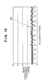
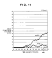
- Figs. 13 and 14 are graphs for explaining temporal transition of electrical charge accumulation
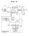
- Fig. 15 is a block diagram showing the arrangement of an image processing apparatus according to the fourth embodiment.
- Fig. 16 is a block diagram showing the arrangement of an image processing apparatus according to the fifth embodiment.
- Fig. 17 is a block diagram showing the arrangement of a conventional image processing apparatus for generating display image data.
- Fig. 18 is a block diagram showing the arrangement of an image processing apparatus proposed by the present applicant for implementing the "sub-frame display method based on spatial frequency separation".
- the first embodiment proposes an improvement in the "sub-frame display method based on spatial frequency separation".
- An image display apparatus which displays display image data generated by an image processing apparatus according to the first embodiment implements the "sub-frame display method based on spatial frequency separation". More specifically, the image display apparatus displays a picture by driving one by one the display elements of a liquid crystal panel having counter electrodes. The image display apparatus separates one frame of a moving picture into a plurality of sub-frames, and executes frame inversion type AC driving to invert the drive polarity for each sub-frame.
- the image display apparatus displays a picture signal having a frame rate of 60 Hz at a display refresh rate of 120 Hz. That is, the image processing apparatus according to the first embodiment generates two sub-frames of a 1/120-sec frame from a signal of a 60-Hz frame rate.
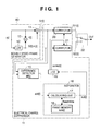
- Fig. 1 is a block diagram showing the arrangement of the image processing apparatus according to the first embodiment.
- a double speed-frame generator 40 generates two sub-frames from an input picture A[i].
- an electrical charge suppressor 11 controls accumulation of electrical charges in the sub-frame period. Details of each unit shown in Fig. 1 will be described later.
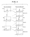
- Fig. 3 shows the waveform of the input picture A[i] shown in Fig. 1 , and the waveforms of signals S1[i] and S2[i] which are generated based on the input picture A[i] and correspond to the first and second sub-frames before correction by the electrical charge suppressor 11. These waveforms are aligned vertically in time series.
- [i] means the ith frame of an input picture or a picture corresponding to the ith frame.
- the arithmetic expressions of the signals S1[i] and S2[i] of sub-frames shown in Fig. 3 will be described later.
- Fig. 3 assume that the object of the input picture A[i] moves to the left at a moving speed V (pixels/frame). If this object is pursued, the moving object seems to be a still picture. If, however, A[i] is displayed for, for example, a 1/60 sec, a motion blur corresponding to this period is observed. To prevent this, the high spatial frequency component which concerns the motion blur (or at which the motion blur becomes conspicuous) is concentrated to one sub-frame by the "sub-frame display method based on spatial frequency separation". This can reduce the motion blur while keeping the low spatial frequency component displayed (e.g., displayed by the two sub-frames), suppressing generation of flicker and a decrease in luminance.
- V moving speed/frame
- Fig. 4A shows a luminance waveform in the "sub-frame display method based on spatial frequency separation". It is apparent from Fig. 4A that the H component (hatched portion) serving as a high spatial frequency component is concentrated to one sub-frame.
- Fig. 4B shows a voltage waveform when double speed-frame inversion is executed in Fig. 4A .
- the luminance waveform reflects the drive voltage, and is equivalent to the absolute value of the voltage waveform. These waveforms will also be called a drive waveform.
- the signal S1[i] corresponding to the first sub-frame is driven by a positive voltage
- the signal S2[i] corresponding to the second sub-frame is driven by a negative voltage.
- Figs. 4A shows a luminance waveform in the "sub-frame display method based on spatial frequency separation”. It is apparent from Fig. 4A that the H component (hatched portion) serving as a high spatial frequency component is concentrated to one sub-frame.
- Fig. 4B shows a
- the H component (hatched portion) serving as a high spatial frequency component is positive to increase the luminance.
- the H component is sometimes negative to decrease the luminance.
- the sub-frame is driven at a frequency obtained by subtracting the H component from an L component (dotted portion) serving as a low spatial frequency component.
- Fig. 4B the DC balance of the entire drive waveform distorts.
- a drive voltage (hatched portion) corresponding to the H component is added to only one sub-frame.
- the positive and negative sides of the voltage waveform are not symmetrical, and the voltage waveform is offset to the positive side by the H component. If the drive waveform has such an offset, a small amount of electrical charges is accumulated in the display element for each frame. A residue image or the like is generated over time, adversely affecting the picture and degrading the liquid crystal characteristic.
- the first embodiment cancels accumulation of electrical charges owing to the distortion of the DC balance by vertically correcting the voltage of the drive waveform while maintaining a predetermined time response characteristic.
- the offset can also be canceled by simply correcting the drive waveform. This is the same as normal frame inversion type driving, and there is no much point in adopting the "sub-frame display method based on spatial frequency separation".
- the first embodiment monitors the offset value of an actual luminance signal per frame, that is, the cumulative value of the difference between the signals of the first and second sub-frames.
- the cumulative value is regarded to be proportional to the actual amount of electrical charge accumulation, and the voltage of the drive waveform is vertically corrected in accordance with the cumulative value, that is, amount of electrical charge accumulation. This can prevent an increase in accumulated electrical charges, and cancel accumulation of electrical charges over time.
- Fig. 17 is a block diagram showing an example of applying the "sub-frame display method based on spatial frequency separation" to a conventional image processing apparatus for generating display image data.
- a lowpass filter (LPF) 12 receives the input picture A[i] of an input frame of interest, and generates a low spatial frequency component L[i]. From the low spatial frequency component L[i] and the original input picture A[i], a subtracter 13 and adder 14 generate a high spatial frequency component H[i], first sub-frame signal S1[i], and second sub-frame signal S2[i] based on the following equations. In other words, the LPF 12, subtracter 13, and adder 14 generate sub-frames.
- LPF() represents a two-dimensional lowpass filter.
- the first sub-frame signal S1[i] and second sub-frame signal S2[i] are sent to the switch 22 which switches at intervals of 1/120 sec, and are alternately output.
- the electrical charge suppressor 11 surrounded by a chain line is added to the conventional arrangement shown in Fig. 17 .
- the electrical charge suppressor 11 monitors the sub-frame signals S1[i] and S2[i] generated by the same way as that in Fig. 17 , and calculates a correction value.
- correctors 20 and 21 generate first and second sub-frame signals S11[i] and S22[i] by correcting the signals S1[i] and S2[i] based on the correction value.
- the corrected signals S11[i] and S22[i] are switched by the switch 22, and alternately output.
- the first and second sub-frame signals S1[i] and S2[i] are input to a difference detector 15.
- the difference detector 15 calculates the difference between these signals, that is, a difference picture diff[i] by subtracting the picture of the second sub-frame from that of the first sub-frame (equation 2-3).
- An integrator 16 integrates the difference picture diff[i] calculated by the difference detector 15 for each frame, and outputs a picture (corrected picture) of a value proportional to the integral value.
- the input difference value is represented as an addition value add[i]
- the output corrected picture is represented as a subtraction value sub[i].
- the integrator 16 includes a calculating unit 17 and frame memory 18, and determines the subtraction value sub[i] representing a sub-frame correction amount based on the addition value add[i] and cumulative value sum[i]. This processing is executed independently for each pixel of image data.
- the correctors 20 and 21 correct the first and second sub-frame signals, respectively.
- the correction value correct[i] is a value obtained by multiplying the subtraction value sub[i] by 1/2 by a multiplier 19 (equation 2-5).
- the correction value correct[i] it is subtracted from the first sub-frame signal (equation 2-6-1), and added to the second sub-frame signal (equation 2-6-2).
- the value obtained by subtracting the second sub-frame signal from the first sub-frame signal becomes smaller by the subtraction value sub[i], and serves as a corrected DC offset value.
- the correction by the correctors 20 and 21 is not limited to addition and subtraction.
- the correctors 20 and 21 suffice to correct the first and second sub-frame signals so as to decrease the difference between their absolute values.
- the frame memory 18 holds the cumulative value sum[i].
- the left side of formula 2-7 represents a change of the cumulative value sum per frame.
- add[i] on the right side is input from the difference detector 15, and added to sum[i] for each frame.
- sub[i] is subtracted from sum[i] for each frame.
- a value obtained by subtracting the subtraction value sub[i] from the addition value add[i] is accumulated as the cumulative value sum[i].
- sub[i] is double the correction value correct[i] in the correctors 20 and 21.
- the first embodiment assumes a system exhibiting a phenomenon similar to charging/discharging of the capacitor, that is, a system which satisfies a first order linear differential equation.
- equations up to formula (2-9) the time axis is represented in the form of the ith frame using [i].
- equation (2-10) is a function of the time using (t). Substituting a predetermined value into add(t) in equation (2-10) yields a solution expressed by an exponential function which starts from an initial value and converges to the predetermined value. Actual calculation is sequentially done in accordance with recurrence formula (2-9) as the frame advances to the next one.
- the proportionality coefficient ⁇ is a positive constant, and is defined as 0 ⁇ ⁇ ⁇ 1.
- the value ⁇ greatly changes the behavior in the first embodiment, so ⁇ needs to be set to an appropriate value in accordance with the characteristics of the liquid crystal panel.
- ⁇ is relatively large, the response of sub[i] to add[i] is quickened, and the cumulative value (corresponding to electrical charges actually accumulated in the device) in the frame memory 18 is suppressed relatively small.
- ⁇ is relatively small, the response of sub[i] to add[i] is slowed, and the cumulative value in the frame memory 18 becomes relatively large.
- a slow response of sub[i] to add[i] is preferable because a problem arising from correction in the embodiment hardly influences the image quality, or the effect of the "sub-frame display method based on spatial frequency separation" is fully exploited. In this case, however, the cumulative value tends to always be large, so the electrical charge accumulation state readily appears in a picture.
- the value ⁇ is desirably set to a proper value depending on the case.
- ⁇ 0.1.
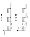
- Fig. 5 shows a picture pattern used in the following description.
- Fig. 5 shows a picture pattern in which a stripe pattern made up of 1-pixel wide dark lines 150 (luminance: 30%) and 1-pixel wide bright lines 151 (luminance: 70%) moves at a speed V of one pixel per frame in a direction perpendicular to the lines 150 and 151.
- the low frequency component L separated by the "sub-frame display method based on spatial frequency separation" represents a luminance of 50%
- the high frequency component H of the bright stripe represents a luminance of 20%
- that of the dark stripe represents a luminance of -20%.
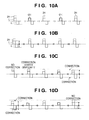
- the drive waveform which pays attention to a specific pixel 152 changes for each frame, as shown in Fig. 10A .
- the distortion of the DC balance between the first and second sub-frames equals 2H. This distortion switches between the positive polarity and the negative polarity every frame, so no electrical charge is accumulated.
- a drive waveform whose DC balance distorts as shown in Fig. 10B is corrected with a predetermined time constant.
- This correction controls the drive waveform to restore the DC balance between the positive and negative directions after a predetermined time (predetermined number of frames).
- a predetermined time predetermined number of frames.
- Fig. 10C is a view showing a state in which correction in the first embodiment starts.
- the left end of Fig. 10C shows a drive waveform (corresponding to an odd-numbered waveform in Fig. 10A or an even-numbered waveform in Fig. 10B ) immediately after the stripe pattern stops moving.
- This drive waveform shifts in the negative direction after a predetermined number of frames, and stabilizes when the correction amount reaches a predetermined value, as shown at the right end of Fig. 10C .
- the correction amount becomes half of 2H, that is, H.
- the DC balance of the drive waveform is restored, preventing further accumulation of electrical charges.
- Fig. 10D shows a drive waveform immediately after the stripe pattern starts moving again from the stopped state. While the picture moves, 2H switches alternately between the positive and negative directions, no electrical charge is accumulated, and no correction need be performed. Hence, after the stripe pattern starts moving, correction is gradually canceled, and the drive waveform returns to one shown at the right end of Fig. 10D after a predetermined number of frames (after four frames in the example of Fig. 10D ).
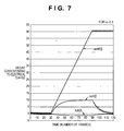
- Figs. 6 and 7 are graphs for explaining temporal transition of electrical charge accumulation.
- the abscissa axis represents the number of frames, and the ordinate axis represents the relative amount when the amount corresponding to electrical charge accumulated by one frame is set to 1. In this case, all parameters can be represented by the same scale. This also applies to Figs. 8 , 9 , 13 , and 14 to be described later.
- the stripe pattern shown in Fig. 5 moves as follows. First, during the period of frame numbers 0 to 30, the stripe pattern shown in Fig. 5 moves at the speed V of one pixel per frame in a direction perpendicular to the lines 150 and 151. During the period of frame numbers 31 to 90, the stripe pattern stops moving. From frame number 91, the stripe pattern starts moving again.
- the addition value add[i] repeats the positive and negative polarities (accumulation and discharging) during the period of frame numbers 0 to 30 and the period from frame number 90, but keeps the positive polarity (accumulation) during the period of frame numbers 31 to 90.
- Fig. 7 shows an uncorrected cumulative value sum0[i] of electrical charges when correction according to the first embodiment is not applied, the cumulative value sum[i] of electrical charges when correction according to the first embodiment is applied, and the subtraction value sub[i].
- the uncorrected cumulative value sum0[i] linearly increases during the period of frame numbers 31 to 90 during which the stripe pattern stands still.
- accumulation of electrical charges exceeds a predetermined level, and a serious problem occurs in the display apparatus such that a residue image remains.
- the subtraction value sub[i] discharge amount
- the cumulative value sum[i] quickly converges, and the value at which the cumulative value sum[i] converges is small.
- the correction amount of the drive waveform acutely changes. For example, even if the luminance level of a specific pixel in a moving picture shows the same value for a very short time, correction acts, and the influence of correction appears and is recognizable as an improper pattern of the moving picture.
- the value ⁇ is desirably set to an optimum value in accordance with the liquid crystal panel.
- the first embodiment vertically corrects the voltage of the drive waveform in accordance with the electrical charge accumulation amount which is the cumulative value of the difference between the first and second sub-frames as an offset value per frame.
- This correction (control) corresponding to the electrical charge accumulation amount is executed in the "sub-frame display method based on spatial frequency separation".
- the first embodiment can prevent an increase in accumulated electrical charges, cancel accumulation of electrical charges, and preferably display a moving picture on the liquid crystal panel.
- the second embodiment according to the present invention will be described.
- the second embodiment will explain electrical charge accumulation control capable of more preferable moving picture playback.
- Fig. 18 is a block diagram showing the arrangement of an image processing apparatus proposed by the present applicant for implementing the "sub-frame display method based on spatial frequency separation".
- the center of gravity of the luminance area changes in the time direction between the display of the high frequency component H[i] and that of the low frequency component L[i], as shown in Fig. 4A .
- This causes an asymmetrical distortion (so-called tailing-blur) in a direction in which a pursued object moves, and an opposite direction.
- generation of the asymmetrical distortion is suppressed by setting the second sub-frame to the average value of the low frequency components of adjacent frames.
- the second embodiment executes the same electrical charge accumulation control as that in the first embodiment so as not to adversely influence the arrangement shown in Fig. 18 .
- an LPF 32 receives an input picture signal A[i] to generate a low spatial frequency component L[i] (equation 3-0). From the low spatial frequency component L[i] and the original input picture signal A[i], a subtracter 33 and adder 34 generate a high spatial frequency component H[i] and first sub-frame signal S1[i] (equations 3-1-1 and 3-1-2).
- a delay circuit (DL) 35 receives the signal S1[i] to output S1[i-1] of an immediately preceding frame.
- a delay circuit (DL) 36 receives L[i] generated by the LPF 32 to output L[i-1] of an immediately preceding frame (equation 3-2).
- An adder 37 adds L[i-1] and L[i], and a multiplier 38 multiplies the sum by 1/2 to generate a second sub-frame signal S2[i-1] of the (i-1)th frame (equation 3-3).
- the first sub-frame signal S1[i] and second sub-frame signal S2[i-1] are sent to a switch 22 which switches at intervals of 1/120 sec, and are alternately output.
- LPF() means that the current frame value is saved and the value of an immediately preceding frame is output.
- LPF() represents a two-dimensional lowpass filter.
- Fig. 2 is a block diagram showing the arrangement of an image processing apparatus according to the second embodiment.
- the image processing apparatus shown in Fig. 2 comprises an electrical charge suppressor 11 which performs the same control as that in the first embodiment.
- a signal sent to the switch 22 is monitored and corrected.
- signals sent to the DLs 35 and 36 are monitored and corrected.
- the signals S11[i-1] and S22[i-1] obtained in this way are alternately output from the switch which switches at intervals of 1/120 sec.
- the second embodiment has described an example of generating the signal S22[i-1] as the average of L[i-1], and L[i] of an immediately succeeding frame. This is an example of displaying (outputting) a signal S22 which contains information of one succeeding frame and is closer to the succeeding frame with respect to the signal S11.
- the second embodiment is also applicable to a case where a signal S22 which contains information of one preceding frame and is closer to the preceding frame. That is, if the signal S11 is not delayed, the signal S22 closer to a preceding frame with respect to the signal S11 is displayed.
- the signal S22 in the second embodiment is the average value of the low frequency components L of the frame i of interest and an immediately preceding frame i-1.
- the signal S22 is the average value of the low frequency components L of the frame i-1 of interest and an immediately succeeding frame i.
- the signal S22 is generated as the average value of the low frequency components L of the frame of interest and either a preceding or succeeding frame temporally adjacent to the frame of interest.
- the second embodiment can execute the same electrical charge accumulation control as that in the first embodiment for the arrangement which implements the "sub-frame display method based on spatial frequency separation" for suppressing an asymmetrical distortion generated in a direction in which a pursued object moves, and an opposite direction.
- the third embodiment according to the present invention will be described.
- the third embodiment will explain an example of inverting a double speed-frame generated by the "intermediate picture insertion method based on motion compensation" serving as the first method of doubling the frame speed, and displaying the inverted frame on a microdisplay.
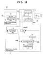
- Fig. 11 is a block diagram showing the arrangement of an image processing apparatus which implements the "sub-frame display method based on spatial frequency separation" according to the third embodiment.
- a double speed-frame generator 30 generates a double speed-picture by the "intermediate picture insertion method based on motion compensation".
- an input picture A[i] is displayed every other sub-frame, and an intermediate picture Sm[i] calculated by motion compensation is displayed between input pictures A[i].
- the difference (addition value add[i]) between A[i] and Sm[i] is input to an integrator 16.
- the operation of the remaining arrangement is the same as that in the first embodiment, and a description thereof will not be repeated.
- the "intermediate picture insertion method based on motion compensation” does not intentionally set a difference between sub-frame signals, unlike the "sub-frame display method based on spatial frequency separation". Hence, no apparent luminance level difference appears between the input picture A[i] and the intermediate picture Sm[i].
- an inserted picture (intermediate picture) generated based on motion prediction is not always, as a picture which forms one frame, a picture of the same luminance level as that of the input picture A[i].
- the third embodiment suppresses an increase in accumulated electrical charges when the luminance levels of an original picture and inserted picture (intermediate picture) statistically differ from each other in a long time in a variety of computational algorithms.
- Fig. 12 shows a drive waveform according to the third embodiment.
- the solid line represents the drive waveform of the input picture A[i] displayed every other frame
- the broken line represents the drive waveform of an inserted image (intermediate picture Sm[i]) inserted between input pictures A[i].
- the difference between the size of the solid line portion and that of the broken line portion i.e., the distortion of the DC balance
- the DC balance may distort after a long time.
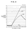
- Figs. 13 and 14 are graphs for explaining temporal transition of electrical charge accumulation when displaying a random picture in the third embodiment.
- the stripe pattern shown in Fig. 5 moves, and no DC offset occurs in the drive waveform.
- the DC balance statically distorts owing to insertion of an intermediate picture into a picture by the "intermediate picture insertion method based on motion compensation".
- accumulation of electrical charges can be controlled to fall within a predetermined level without increasing the cumulative value sum[i], as shown in Fig. 14 .
- the third embodiment is not limited to a double speed-frame according to the "intermediate picture insertion method based on motion compensation".
- the third embodiment is applicable to any double-speed frame display apparatus which performs frame inversion and may statically suffer the distortion of the DC balance.
- a feature of the fourth embodiment is to further reduce the difference between a cumulative value sum[i] representing the accumulation state of electrical charges in a frame memory 18, and the actual accumulation state of electrical charges on a liquid crystal display.
- Fig. 15 is a block diagram showing the arrangement of an image processing apparatus which implements the "sub-frame display method based on spatial frequency separation" according to the fourth embodiment.
- the arrangement shown in Fig. 15 is the same as those in the above-described embodiments in that correctors 20 and 21 correct a first sub-frame signal S1[i] and second sub-frame signal S2[i] supplied from a double speed-frame generator 40 to suppress accumulation of electrical charges.
- the arrangement shown in Fig. 15 further comprises a saturation preventer 23 for calculating a remaining correction amount after correction by the correctors 20 and 21.
- the saturation preventer 23 returns the remaining correction amount to an integrator 16, and the integrator 16 feeds it back to the cumulative value sum[i].
- the calculated luminance level of a sub-frame (first sub-frame), to which the high frequency component H is concentrated sometimes exceeds the maximum value (100% level). In this case, the excess over the maximum value is moved to the other sub-frame (second sub-frame). Also, the calculated luminance level of the first sub-frame sometimes becomes lower than 0 level. In this case, a luminance component corresponding to the shortage is moved from the second sub-frame.
- the saturation preventer 23 controls this moving processing.
- the range of the maximum value to 0 level is the allowable range of the pixel level.
- S1[i] and S2[i] represent outputs from the double speed-frame generator 40
- S11[i] represents an output from the corrector 20
- S22[i] represents an output from the corrector 21
- S111[i] and S222[i] represent outputs from the saturation preventer 23.
- Saturation processing by the saturation preventer 23 in the fourth embodiment is given as a function Sat() in equations (5-2-1) and (5-2-2):
- S ⁇ 111 i Sat ⁇ 1 S ⁇ 11 i , S ⁇ 22 i
- S ⁇ 222 i Sat ⁇ 2 S ⁇ 11 i , S ⁇ 22 i
- the feedback value add2[i] is defined in this fashion.
- the saturation preventer 23 corrects the pixel level of a sub-frame to fall within the allowable range. This can greatly reduce the difference between an electrical charge accumulation amount virtually reproduced in the frame memory 18, and an electrical charge accumulation amount actually accumulated in the device. Compared to the first embodiment, the fourth embodiment can display a higher-quality moving picture on the liquid crystal panel.
- the electrical charge suppressor 11 is configured on the assumption that electrical charges are accumulated in proportion to the level difference between the first and second sub-frames.
- the level difference can be regarded as the level difference between display luminances or that between image data.
- accumulation of electrical charges is not accurately proportional to the level difference between image data or that between display luminances, and has a nonlinear relationship with them.
- the fifth embodiment monitors and corrects the first and second sub-frames in consideration of the nonlinear relationship.
- Fig. 16 is a block diagram showing an arrangement for implementing the "sub-frame display method based on spatial frequency separation" according to the fifth embodiment. Similar to the electrical charge suppressor 11 in the above-described embodiments, an electrical charge suppressor 55 in the fifth embodiment monitors and corrects the first and second sub-frame signals.
- nonlinear converters 51 and 52 In the electrical charge suppressor 55, nonlinear converters 51 and 52 generate signals Sv1[i] and Sv2[i] by performing predetermined nonlinear conversion for first and second sub-frame signals S1[i] and S2[i], and send the signals Sv1[i] and Sv2[i] to a difference detector 15.
- the nonlinear conversion by the nonlinear converters 51 and 52 is the first conversion, and the first conversion converts a signal value into an amount of electrical charge accumulation.
- a subtraction signal sub[i] calculated by an integrator 16 is not simply halved, unlike the first embodiment, but undergoes predetermined nonlinear conversion by nonlinear converters 53 and 54.
- the nonlinear conversion by the nonlinear converters 53 and 54 is the second conversion.
- the second conversion is inverse conversion corresponding to the first conversion, and converts an amount of electrical charge accumulation into a signal value.
- the nonlinear converters 53 and 54 calculate correction amounts correct1[i] and correct2[i] for respective sub-frames. Based on correct1[i] and correct2[i], correctors 20 and 21 correct the first and second sub-frames.
- the nonlinear converters 51 to 54 suffice to be formed from lookup tables representing the relationship between signal values and amounts of electrical charge accumulation.
- the fifth embodiment calculates the correction values of the first and second sub-frame signals by executing nonlinear conversion for the first and second sub-frame signals in consideration of the nonlinear relationship representing the signal value and the electrical charge amount.
- the fifth embodiment can achieve more accurate electrical charge accumulation control.
- the present invention can be applied to a system constituted by a plurality of devices (e.g., host computer, interface, reader, printer) or to an apparatus comprising a single device (e.g., copying machine, facsimile machine).
- devices e.g., host computer, interface, reader, printer
- apparatus comprising a single device (e.g., copying machine, facsimile machine).
- the present invention can provide a storage medium storing program code for performing the above-described processes to a computer system or apparatus (e.g., a personal computer), reading the program code, by a CPU or MPU of the computer system or apparatus, from the storage medium, then executing the program.
- a computer system or apparatus e.g., a personal computer
- reading the program code by a CPU or MPU of the computer system or apparatus, from the storage medium, then executing the program.
- the program code read from the storage medium realizes the functions according to the embodiments.
- the storage medium such as a floppy disk, a hard disk, an optical disk, a magnetooptical disk, CD-ROM, CD-R, a magnetic tape, a nonvolatile type memory card, and ROM can be used for providing the program code.
- the present invention includes a case where an OS (operating system) or the like working on the computer performs a part or entire processes in accordance with designations of the program code and realizes functions according to the above embodiments.
- the present invention also includes a case where, after the program code read from the storage medium is written in a function expansion card which is inserted into the computer or in a memory provided in a function expansion unit which is connected to the computer, CPU or the like contained in the function expansion card or unit performs a part or entire process in accordance with designations of the program code and realizes functions of the above embodiments.
- the storage medium stores program code corresponding to the flowcharts described in the embodiments.
Description
- The present invention relates to an image processing apparatus and image processing method for generating image data to be supplied to an image display apparatus which inverts the drive polarity of display elements in each of plural sub-frames formed from a frame of a moving picture to display the moving picture.
- A cathode ray tube (CRT) has been synonymous with a moving picture display device for a television and the like. However, liquid crystal displays (LCDs), plasma displays (PDPs), and field emission displays (FEDs) have been put into practical use in recent years. There are displays of various display types now. The displays of these types adopt different display methods. For example, display devices based on a liquid crystal display (e.g., a direct viewing type LCD, liquid crystal rear projector, and liquid crystal front projector) use many scanning methods. In any case, the period of outputting light in each pixel portion occupies a large part of one frame. For this reason, such a display is called a hold-type display.
- On the other hand, in a CRT or FED, light is output in each pixel portion once in a frame. The period of emitting light is much shorter than the frame length and is normally 2 msec or less. For this reason, such a display is called an impulse-type display.
- There also exist a PDP and field sequential display (FSD) which are of types different from the above-mentioned classes.
- The hold-type display and impulse-type display have the following features.
- The hold-type display: A display of this type emits light during a large part of the frame period. Hence, temporal variations of light intensity are small, and flicker is rarely observed. However, pursuit (pursuing a moving portion in a moving picture by eyes) makes the motion blur relatively large in accordance with the length of the period of emitting light in a frame. This motion blur here is different from that caused by the response characteristic of a display device.
- The impulse-type display: A display of this type has a very short period of emitting light in a frame. Hence, temporal variations of light intensity are large, and flicker synchronous with a frame is observed. However, the motion blur in pursuit is rarely observed. It is, therefore, possible to obtain a resolution almost equal to that of a still object.
- In general, the period of emitting light in a display changes depending on the display method and display device. The hold-type display and impulse-type display are poles apart in terms of in the period of emitting light. The period of emitting light and the degree of motion blur are almost proportional to each other. Longer periods of light emission result in larger amounts of motion blur. Shorter periods of light emission result in smaller amounts of motion blur. On the other hand, concerning flicker synchronous with a frame, longer periods of light emission result in smaller flicker. Shorter periods of light emission result in larger flicker. In this manner, the motion blur and flicker have trade-off relationships with respect to the period of emitting light.
- A solution to the motion blur and flicker is multiplying the frame frequency by N. In many cases, N = 2. That is, the frame frequency is doubled. When the frame frequency is doubled, the period of emitting light in each double speed-frame is halved. This also almost halves the motion blur. Regarding flicker as well, if an initial frame frequency of 60 Hz is doubled to 120 Hz, the frame frequency falls outside the response characteristic of human eyes. Hence, no flicker is observed.
- As described above, multiplying the frame frequency by N has a large effect but poses a new problem.
- For example, when the frame frequency of an original picture signal is 60 Hz, the picture information is updated every 1/60 sec. If the frame frequency is doubled to display a picture at 120 Hz, necessary picture information is missing every other frame. As a measure, identical pictures are displayed, for example, twice if the frame frequency is doubled. This solves flicker but cannot improve the motion blur in the original picture. In an impulse-type display, double pictures are observed by pursuit.
- To double the frame frequency, two methods are mainly used.
- The first method detects the motion of an object in an original picture and predicts pictures between two frames. This is generally called an "intermediate picture insertion method based on motion compensation". In the first method, the amount of calculation is enormous, and a prediction error occurs under a specific condition.
- In the second method, first, filtering is performed for each frame of an input picture to separate the spatial frequency into a high frequency component which greatly concerns the motion blur and a low frequency component which greatly concerns flicker. Then, the high frequency component is concentrated to one sub-frame (one of two double speed-frames corresponding to the original frame). The low frequency component is distributed to both sub-frames (both of the two double speed-frames corresponding to the original frame). The second method will be called a "sub-frame display method based on spatial frequency separation".
- In a display using a liquid crystal panel, if the liquid crystal panel is driven while the DC balance is disturbed, electrical charges are accumulated between electrodes to degrade the image quality. To avoid this, the drive polarity of the liquid crystal panel is inverted every predetermined cycle to cancel the DC offset of the voltage applied between electrodes. The inversion cycle is one frame or a sub-frame obtained by uniformly dividing one frame.
- When AC drive is performed to invert the polarity for each frame or sub-frame (to be referred to as frame inversion hereinafter), a pair of polarity-inverted displays need to be the same picture considering the purpose of avoiding the DC offset every pixel. However, even if signals are identical, the display sensitivity or non-linear characteristic to the drive voltage is not always the same or symmetrical between a case where the device is driven by a positive voltage and a case where it is driven by a negative voltage. The luminance slightly changes between these two cases, causing flicker.
- To cancel the flicker, a direct viewing type LCD executes the above-described frame inversion, and at the same time, executes spatial polarity inversion, that is, pixel inversion to invert the polarity for each display element (pixel) (e.g., in a staggered pattern). Alternatively, the direct viewing type LCD executes line inversion to invert the polarity for each vertical or horizontal line.
- This pixel inversion or line inversion causes the following problems in a method of performing projection display using a microdisplay, like a rear projector or front projector. That is, the electric field leaks between inverted areas (so-called disclination), adversely affecting the display picture. To prevent this, the microdisplay performs only temporal polarity inversion, that is, frame inversion without performing spatial polarity inversion, that is, pixel inversion or line inversion. Hence, the microdisplay suffers flicker.
- To make flicker unobserved by the user, the microdisplay doubles the flicker frequency by doubling the refresh rate of the display. For example, when the frame frequency of an original picture to be displayed is 60 Hz, the refresh rate of the display device is set to 120 Hz to set the flicker frequency to 120 Hz. The 120-Hz flicker greatly exceeds the limit of the frequency recognizable by human eyes, so the problem of flicker is solved.
- If the speed of the display device is doubled and 120-Hz frame inversion (to be referred to as double speed-frame inversion hereinafter) is done in order to practice the "sub-frame display method based on spatial frequency separation", the following problem arises. That is, in double speed-frame inversion, a picture when driving the liquid crystal panel by a positive voltage and that when driving the panel by a negative voltage are different from each other. Thus, the DC balance in driving distorts in each pixel. In a liquid crystal microdisplay or the like, electrical charges are accumulated in each display element, and the residue image of a preceding picture appears.
- To solve this problem, the polarity may also be inverted in a longer cycle separately from double speed-frame inversion. If the polarity is inverted in a long cycle, changes of the luminance and color stand out, degrading the image quality.
-
US 2005/078069 discloses an active matrix type display panel which is a hold type display panel which has a plurality of pixels arranged in a matrix form, and holds and displays an electrical signal pixel by pixel for a predetermined time. A frame rate conversion circuit converts a video signal having a first vertical frequency (60 Hz) into a video signal having a second vertical frequency (120 Hz) which is m/n-fold (wherein m is an integer of 2 or more, n is an integer of 1 or more, and conditions of m>n are satisfied) of the first vertical frequency. A time base emphasizing circuit subjects an output from the frame rate conversion circuit to time base emphasis. A drive circuit displays the video signal having the second vertical frequency in a display panel. -
EP 1 777 939 -
US 7 202 843 discloses a method for driving a liquid crystal display (LCD) panel which includes receiving continuously a plurality of frame data, generating a plurality of data impulses for each pixel every frame period according to the frame data, and applying the data impulses to a liquid crystal device of a pixel within a frame period via the data line connected to the pixel in order to control a transmission rate of the liquid crystal device. - According to a first aspect of the present invention, there is provided an image processing apparatus according to
claim 1. - According to a second aspect of the present invention, there is provided a method for an image processing apparatus according to
claim 10. - According to these aspects, in an image display apparatus for inverting the drive polarity for each sub-frame to display a picture, even if the pictures of adjacent sub-frames are different from each other, image data which suppresses accumulation of electrical charges in each display element can be generated.
- Further features of the present invention will become apparent from the following description of exemplary embodiments with reference to the attached drawings.
-
Fig. 1 is a block diagram showing the arrangement of an image processing apparatus according to the first embodiment; -
Fig. 2 is a block diagram showing the arrangement of an image processing apparatus according to the second embodiment; -
Fig. 3 is a graph showing an example of the waveforms of the images of an input frame and sub-frame along the time axis; -
Fig. 4A is a graph showing an example of the luminance waveform in the "sub-frame display method based on spatial frequency separation"; -
Fig. 4B is a graph showing an example of the voltage waveform when double speed-frame inversion is executed inFig. 4A ; -
Fig. 5 is a view showing an example of the picture pattern; -
Figs. 6 to 9 are graphs for explaining temporal transition of electrical charge accumulation; -
Figs. 10A to 10D are waveform charts showing examples of the drive waveform of frame inversion type AC driving according to the first embodiment; -
Fig. 11 is a block diagram showing the arrangement of an image processing apparatus according to the third embodiment; -
Fig. 12 is a waveform chart showing an example of the drive waveform of frame inversion type AC driving according to the third embodiment; -
Figs. 13 and14 are graphs for explaining temporal transition of electrical charge accumulation; -
Fig. 15 is a block diagram showing the arrangement of an image processing apparatus according to the fourth embodiment; -
Fig. 16 is a block diagram showing the arrangement of an image processing apparatus according to the fifth embodiment; -
Fig. 17 is a block diagram showing the arrangement of a conventional image processing apparatus for generating display image data; and -
Fig. 18 is a block diagram showing the arrangement of an image processing apparatus proposed by the present applicant for implementing the "sub-frame display method based on spatial frequency separation". - The present invention will be described in detail below based on preferred embodiments with reference to the accompanying drawings. Arrangements set forth in the following embodiments are merely examples, and the present invention is not limited to the illustrated arrangements.
- An outline of the first embodiment according to the present invention will be explained. The first embodiment proposes an improvement in the "sub-frame display method based on spatial frequency separation".
- An image display apparatus which displays display image data generated by an image processing apparatus according to the first embodiment implements the "sub-frame display method based on spatial frequency separation". More specifically, the image display apparatus displays a picture by driving one by one the display elements of a liquid crystal panel having counter electrodes. The image display apparatus separates one frame of a moving picture into a plurality of sub-frames, and executes frame inversion type AC driving to invert the drive polarity for each sub-frame.
- The image display apparatus according to the first embodiment displays a picture signal having a frame rate of 60 Hz at a display refresh rate of 120 Hz. That is, the image processing apparatus according to the first embodiment generates two sub-frames of a 1/120-sec frame from a signal of a 60-Hz frame rate.
-
Fig. 1 is a block diagram showing the arrangement of the image processing apparatus according to the first embodiment. In the image processing apparatus, a double speed-frame generator 40 generates two sub-frames from an input picture A[i]. When outputting the two sub-frames via aswitch 22, anelectrical charge suppressor 11 controls accumulation of electrical charges in the sub-frame period. Details of each unit shown inFig. 1 will be described later. -
Fig. 3 shows the waveform of the input picture A[i] shown inFig. 1 , and the waveforms of signals S1[i] and S2[i] which are generated based on the input picture A[i] and correspond to the first and second sub-frames before correction by theelectrical charge suppressor 11. These waveforms are aligned vertically in time series. [i] means the ith frame of an input picture or a picture corresponding to the ith frame. The arithmetic expressions of the signals S1[i] and S2[i] of sub-frames shown inFig. 3 will be described later. - In
Fig. 3 , assume that the object of the input picture A[i] moves to the left at a moving speed V (pixels/frame). If this object is pursued, the moving object seems to be a still picture. If, however, A[i] is displayed for, for example, a 1/60 sec, a motion blur corresponding to this period is observed. To prevent this, the high spatial frequency component which concerns the motion blur (or at which the motion blur becomes conspicuous) is concentrated to one sub-frame by the "sub-frame display method based on spatial frequency separation". This can reduce the motion blur while keeping the low spatial frequency component displayed (e.g., displayed by the two sub-frames), suppressing generation of flicker and a decrease in luminance. -
Fig. 4A shows a luminance waveform in the "sub-frame display method based on spatial frequency separation". It is apparent fromFig. 4A that the H component (hatched portion) serving as a high spatial frequency component is concentrated to one sub-frame.Fig. 4B shows a voltage waveform when double speed-frame inversion is executed inFig. 4A . The luminance waveform reflects the drive voltage, and is equivalent to the absolute value of the voltage waveform. These waveforms will also be called a drive waveform. InFig. 4B , the signal S1[i] corresponding to the first sub-frame is driven by a positive voltage, whereas the signal S2[i] corresponding to the second sub-frame is driven by a negative voltage. InFigs. 4A and 4B , the H component (hatched portion) serving as a high spatial frequency component is positive to increase the luminance. However, the H component is sometimes negative to decrease the luminance. When the H component is negative, the sub-frame is driven at a frequency obtained by subtracting the H component from an L component (dotted portion) serving as a low spatial frequency component. - In
Fig. 4B , the DC balance of the entire drive waveform distorts. A drive voltage (hatched portion) corresponding to the H component is added to only one sub-frame. Thus, the positive and negative sides of the voltage waveform are not symmetrical, and the voltage waveform is offset to the positive side by the H component. If the drive waveform has such an offset, a small amount of electrical charges is accumulated in the display element for each frame. A residue image or the like is generated over time, adversely affecting the picture and degrading the liquid crystal characteristic. - The first embodiment cancels accumulation of electrical charges owing to the distortion of the DC balance by vertically correcting the voltage of the drive waveform while maintaining a predetermined time response characteristic.
- The offset can also be canceled by simply correcting the drive waveform. This is the same as normal frame inversion type driving, and there is no much point in adopting the "sub-frame display method based on spatial frequency separation".
- The first embodiment monitors the offset value of an actual luminance signal per frame, that is, the cumulative value of the difference between the signals of the first and second sub-frames. The cumulative value is regarded to be proportional to the actual amount of electrical charge accumulation, and the voltage of the drive waveform is vertically corrected in accordance with the cumulative value, that is, amount of electrical charge accumulation. This can prevent an increase in accumulated electrical charges, and cancel accumulation of electrical charges over time.
- Prior to a detailed description of the basic operation of the first embodiment, a prior art corresponding to the embodiment will be explained for easy understanding of the embodiment.
-
Fig. 17 is a block diagram showing an example of applying the "sub-frame display method based on spatial frequency separation" to a conventional image processing apparatus for generating display image data. InFig. 17 , a lowpass filter (LPF) 12 receives the input picture A[i] of an input frame of interest, and generates a low spatial frequency component L[i]. From the low spatial frequency component L[i] and the original input picture A[i], asubtracter 13 andadder 14 generate a high spatial frequency component H[i], first sub-frame signal S1[i], and second sub-frame signal S2[i] based on the following equations. In other words, theLPF 12,subtracter 13, andadder 14 generate sub-frames. In the following equations, LPF() represents a two-dimensional lowpass filter.


- In
Fig. 17 , the first sub-frame signal S1[i] and second sub-frame signal S2[i] are sent to theswitch 22 which switches at intervals of 1/120 sec, and are alternately output. - The operation of the image processing apparatus according to the first embodiment will be explained with reference to
Fig. 1 . In the arrangement ofFig. 1 , theelectrical charge suppressor 11 surrounded by a chain line is added to the conventional arrangement shown inFig. 17 . In the arrangement shown inFig. 1 , theelectrical charge suppressor 11 monitors the sub-frame signals S1[i] and S2[i] generated by the same way as that inFig. 17 , and calculates a correction value. Then,correctors switch 22, and alternately output. - The arrangement and operation of the
electrical charge suppressor 11 will be explained. - The first and second sub-frame signals S1[i] and S2[i] are input to a
difference detector 15. Thedifference detector 15 calculates the difference between these signals, that is, a difference picture diff[i] by subtracting the picture of the second sub-frame from that of the first sub-frame (equation 2-3). - An
integrator 16 integrates the difference picture diff[i] calculated by thedifference detector 15 for each frame, and outputs a picture (corrected picture) of a value proportional to the integral value. In the following description, the input difference value is represented as an addition value add[i], and the output corrected picture is represented as a subtraction value sub[i].

- The
integrator 16 includes a calculatingunit 17 andframe memory 18, and determines the subtraction value sub[i] representing a sub-frame correction amount based on the addition value add[i] and cumulative value sum[i]. This processing is executed independently for each pixel of image data. - The
correctors 


- The correction by the
correctors correctors - Procedures to calculate the subtraction value sub[i] and the cumulative value sum[i] of the difference picture by the
integrator 16 will be explained. All calculation operations are done independently for each pixel, and are not correlated between pixels. - The calculating
unit 17 executes calculation based on a recurrence formula (2-7):
frame memory 18 holds the cumulative value sum[i]. - The left side of formula 2-7 represents a change of the cumulative value sum per frame. add[i] on the right side is input from the
difference detector 15, and added to sum[i] for each frame. sub[i] is subtracted from sum[i] for each frame. In other words, a value obtained by subtracting the subtraction value sub[i] from the addition value add[i] is accumulated as the cumulative value sum[i]. From equation (2-5), sub[i] is double the correction value correct[i] in thecorrectors - A method of determining the subtraction value sub[i] in the
integrator 16 will be explained. The first embodiment assumes a system exhibiting a phenomenon similar to charging/discharging of the capacitor, that is, a system which satisfies a first order linear differential equation. - The discharge amount (subtraction amount) sub[i] must be defined as an amount proportional to the cumulative value sum[i] at that time:


- In equations up to formula (2-9), the time axis is represented in the form of the ith frame using [i]. To the contrary, equation (2-10) is a function of the time using (t). Substituting a predetermined value into add(t) in equation (2-10) yields a solution expressed by an exponential function which starts from an initial value and converges to the predetermined value. Actual calculation is sequentially done in accordance with recurrence formula (2-9) as the frame advances to the next one.
- The proportionality coefficient α is a positive constant, and is defined as 0 < α < 1. The value α greatly changes the behavior in the first embodiment, so α needs to be set to an appropriate value in accordance with the characteristics of the liquid crystal panel. When α is relatively large, the response of sub[i] to add[i] is quickened, and the cumulative value (corresponding to electrical charges actually accumulated in the device) in the
frame memory 18 is suppressed relatively small. When α is relatively small, the response of sub[i] to add[i] is slowed, and the cumulative value in theframe memory 18 becomes relatively large. - A slow response of sub[i] to add[i] is preferable because a problem arising from correction in the embodiment hardly influences the image quality, or the effect of the "sub-frame display method based on spatial frequency separation" is fully exploited. In this case, however, the cumulative value tends to always be large, so the electrical charge accumulation state readily appears in a picture.
- From this, the value α is desirably set to a proper value depending on the case. In the following concrete example, α = 0.1.
- A concrete operation in the first embodiment will be described below.
Fig. 5 shows a picture pattern used in the following description.Fig. 5 shows a picture pattern in which a stripe pattern made up of 1-pixel wide dark lines 150 (luminance: 30%) and 1-pixel wide bright lines 151 (luminance: 70%) moves at a speed V of one pixel per frame in a direction perpendicular to thelines - Since the stripe pattern shown in
Fig. 5 moves at the speed V of one pixel per frame, the drive waveform which pays attention to aspecific pixel 152 changes for each frame, as shown inFig. 10A . In this case, the distortion of the DC balance between the first and second sub-frames equals 2H. This distortion switches between the positive polarity and the negative polarity every frame, so no electrical charge is accumulated. - However, if the stripe pattern stops moving while the distortion of 2H is positive, the DC balance of the drive waveform, which pays attention to the
pixel 152, is kept distorted by 2H in the positive direction. In this case, electrical charges are accumulated in the positive direction in thepixel 152. In contrast, if the stripe pattern stops moving while the distortion of 2H is negative, the DC balance of the drive waveform, which pays attention to thepixel 152, is kept distorted by 2H in the negative direction. Electrical charges are accumulated in the negative direction in thepixel 152. - According to the first embodiment, a drive waveform whose DC balance distorts as shown in
Fig. 10B is corrected with a predetermined time constant. This correction controls the drive waveform to restore the DC balance between the positive and negative directions after a predetermined time (predetermined number of frames). When the distortion of the DC balance of the drive waveform is canceled, further accumulation of electrical charges is suppressed. Correction processing in the first embodiment will be described below. -
Fig. 10C is a view showing a state in which correction in the first embodiment starts. The left end ofFig. 10C shows a drive waveform (corresponding to an odd-numbered waveform inFig. 10A or an even-numbered waveform inFig. 10B ) immediately after the stripe pattern stops moving. This drive waveform shifts in the negative direction after a predetermined number of frames, and stabilizes when the correction amount reaches a predetermined value, as shown at the right end ofFig. 10C . At the right end ofFig. 10C , that is, when the drive waveform reaches the stable state, the correction amount becomes half of 2H, that is, H. At this timing, the DC balance of the drive waveform is restored, preventing further accumulation of electrical charges. - The left end of
Fig. 10D shows a drive waveform immediately after the stripe pattern starts moving again from the stopped state. While the picture moves, 2H switches alternately between the positive and negative directions, no electrical charge is accumulated, and no correction need be performed. Hence, after the stripe pattern starts moving, correction is gradually canceled, and the drive waveform returns to one shown at the right end ofFig. 10D after a predetermined number of frames (after four frames in the example ofFig. 10D ). - As long as the stripe pattern moves, 2H repeats the positive and negative polarities, and the state in which no DC balance distorts can be maintained.
-
Figs. 6 and7 are graphs for explaining temporal transition of electrical charge accumulation.Fig. 7 shows a case where α = 0.1 in formula (2-9). InFigs. 6 and7 , the abscissa axis represents the number of frames, and the ordinate axis represents the relative amount when the amount corresponding to electrical charge accumulated by one frame is set to 1. In this case, all parameters can be represented by the same scale. This also applies toFigs. 8 ,9 ,13 , and14 to be described later. - The stripe pattern shown in
Fig. 5 moves as follows. First, during the period offrame numbers 0 to 30, the stripe pattern shown inFig. 5 moves at the speed V of one pixel per frame in a direction perpendicular to thelines frame numbers 31 to 90, the stripe pattern stops moving. From frame number 91, the stripe pattern starts moving again. -
Fig. 6 shows a change of the addition value add[i] (= diff[i]) in the stripe pattern. As shown inFig. 6 , the addition value add[i] repeats the positive and negative polarities (accumulation and discharging) during the period offrame numbers 0 to 30 and the period fromframe number 90, but keeps the positive polarity (accumulation) during the period offrame numbers 31 to 90. -
Fig. 7 shows an uncorrected cumulative value sum0[i] of electrical charges when correction according to the first embodiment is not applied, the cumulative value sum[i] of electrical charges when correction according to the first embodiment is applied, and the subtraction value sub[i]. - As shown in
Fig. 7 , the uncorrected cumulative value sum0[i] linearly increases during the period offrame numbers 31 to 90 during which the stripe pattern stands still. In a general liquid crystal microdisplay, if this state continues for several minutes, accumulation of electrical charges exceeds a predetermined level, and a serious problem occurs in the display apparatus such that a residue image remains. - Even at the cumulative value sum[i] when correction according to the first embodiment is applied, accumulation of electrical charges starts immediately after the stripe pattern stops moving (near
frame numbers 30 to 40). After that (after 20 to 30 frames), accumulated electrical charges reach a predetermined value, and then accumulation of electrical charges is suppressed. - From frame number 91, the stripe pattern starts moving again. The cumulative value sum[i], which has reached the equilibrium point, starts decreasing (electrical charges are discharged), and converges to 0 (state in which no electrical charge is accumulated). Even if the stripe pattern keeps still from frame number 91, accumulated electrical charges do not increase once they have reached the equilibrium point. To the contrary, if the stripe pattern keeps still, the uncorrected cumulative value sum0[i] increases, and even if the stripe pattern starts moving again, it maintains a value (accumulated electrical charges) at the restart point. In short, unless correction according to the first embodiment is executed, no accumulated electrical charge is discharged as long as the stripe pattern is repeated.
- In
Fig. 7 , the curve shown at the bottom represents the subtraction value sub[i]. Since α = 0.1, the subtraction value sub[i] is 1/10 of the cumulative value sum[i], and has an opposite sign. After accumulated electrical charges reach the equilibrium point nearframe number 60, the addition value add[i] (Fig. 6 ) and subtraction value sub[i] (Fig. 7 ) converge to the same value. - The first embodiment has described the case where α = 0.1. A behavior when α is set to a slightly large or small value will be explained.
-
Fig. 8 shows a case where α = 0.01.Fig. 9 shows a case where α = 0.5. - As shown in
Fig. 8 , when α is relatively small, the subtraction value sub[i] (discharge amount) is small. The cumulative value sum[i] does not quickly converge, and the value at which the cumulative value sum[i] converges is large. If the convergence value is excessively large, a residue image as described above appears. Even if the picture starts moving again, a long time is taken to decrease the cumulative value sum[i] (discharge electrical charges), and this poor response characteristic influences the picture. - As shown in
Fig. 9 , when α is relatively large, the subtraction value sub[i] (discharge amount) is large. The cumulative value sum[i] quickly converges, and the value at which the cumulative value sum[i] converges is small. In this case, the correction amount of the drive waveform acutely changes. For example, even if the luminance level of a specific pixel in a moving picture shows the same value for a very short time, correction acts, and the influence of correction appears and is recognizable as an improper pattern of the moving picture. - As described above, an excessively small or large value α adversely influences the image quality, so the value α is desirably set to an optimum value in accordance with the liquid crystal panel.
- As described above, the first embodiment vertically corrects the voltage of the drive waveform in accordance with the electrical charge accumulation amount which is the cumulative value of the difference between the first and second sub-frames as an offset value per frame. This correction (control) corresponding to the electrical charge accumulation amount is executed in the "sub-frame display method based on spatial frequency separation". The first embodiment can prevent an increase in accumulated electrical charges, cancel accumulation of electrical charges, and preferably display a moving picture on the liquid crystal panel.
- The second embodiment according to the present invention will be described. The second embodiment will explain electrical charge accumulation control capable of more preferable moving picture playback.
- The present applicant has proposed a technique which improves the conventional "sub-frame display method based on spatial frequency separation" shown in
Fig. 17. Fig. 18 is a block diagram showing the arrangement of an image processing apparatus proposed by the present applicant for implementing the "sub-frame display method based on spatial frequency separation". - In the arrangement shown in
Fig. 17 , the center of gravity of the luminance area changes in the time direction between the display of the high frequency component H[i] and that of the low frequency component L[i], as shown inFig. 4A . This causes an asymmetrical distortion (so-called tailing-blur) in a direction in which a pursued object moves, and an opposite direction. In the arrangement shown inFig. 18 , generation of the asymmetrical distortion is suppressed by setting the second sub-frame to the average value of the low frequency components of adjacent frames. The second embodiment executes the same electrical charge accumulation control as that in the first embodiment so as not to adversely influence the arrangement shown inFig. 18 . - In the arrangement shown in
Fig. 18 , anLPF 32 receives an input picture signal A[i] to generate a low spatial frequency component L[i] (equation 3-0). From the low spatial frequency component L[i] and the original input picture signal A[i], asubtracter 33 andadder 34 generate a high spatial frequency component H[i] and first sub-frame signal S1[i] (equations 3-1-1 and 3-1-2). A delay circuit (DL) 35 receives the signal S1[i] to output S1[i-1] of an immediately preceding frame. A delay circuit (DL) 36 receives L[i] generated by theLPF 32 to output L[i-1] of an immediately preceding frame (equation 3-2). Anadder 37 adds L[i-1] and L[i], and amultiplier 38 multiplies the sum by 1/2 to generate a second sub-frame signal S2[i-1] of the (i-1)th frame (equation 3-3). The first sub-frame signal S1[i] and second sub-frame signal S2[i-1] are sent to aswitch 22 which switches at intervals of 1/120 sec, and are alternately output. - In the following equations, DL() means that the current frame value is saved and the value of an immediately preceding frame is output. LPF() represents a two-dimensional lowpass filter.


-
Fig. 2 is a block diagram showing the arrangement of an image processing apparatus according to the second embodiment. In addition to the arrangement shown inFig. 18 , the image processing apparatus shown inFig. 2 comprises anelectrical charge suppressor 11 which performs the same control as that in the first embodiment. In the first embodiment, a signal sent to theswitch 22 is monitored and corrected. In the second embodiment, signals sent to theDLs - The signals S11[i-1] and S22[i-1] obtained in this way are alternately output from the switch which switches at intervals of 1/120 sec.
- All arithmetic expressions in the arrangement shown in
Fig. 2 are


- The second embodiment has described an example of generating the signal S22[i-1] as the average of L[i-1], and L[i] of an immediately succeeding frame. This is an example of displaying (outputting) a signal S22 which contains information of one succeeding frame and is closer to the succeeding frame with respect to the signal S11. However, the second embodiment is also applicable to a case where a signal S22 which contains information of one preceding frame and is closer to the preceding frame. That is, if the signal S11 is not delayed, the signal S22 closer to a preceding frame with respect to the signal S11 is displayed. Letting i be the frame of interest of the signal S11, the signal S22 in the second embodiment is the average value of the low frequency components L of the frame i of interest and an immediately preceding frame i-1. Letting i-1 be the frame of interest of the signal S11, the signal S22 is the average value of the low frequency components L of the frame i-1 of interest and an immediately succeeding frame i. In other words, the signal S22 is generated as the average value of the low frequency components L of the frame of interest and either a preceding or succeeding frame temporally adjacent to the frame of interest.
- As described above, the second embodiment can execute the same electrical charge accumulation control as that in the first embodiment for the arrangement which implements the "sub-frame display method based on spatial frequency separation" for suppressing an asymmetrical distortion generated in a direction in which a pursued object moves, and an opposite direction.
- The third embodiment according to the present invention will be described. The third embodiment will explain an example of inverting a double speed-frame generated by the "intermediate picture insertion method based on motion compensation" serving as the first method of doubling the frame speed, and displaying the inverted frame on a microdisplay.
-
Fig. 11 is a block diagram showing the arrangement of an image processing apparatus which implements the "sub-frame display method based on spatial frequency separation" according to the third embodiment. InFig. 11 , a double speed-frame generator 30 generates a double speed-picture by the "intermediate picture insertion method based on motion compensation". As the double speed-picture in the third embodiment, an input picture A[i] is displayed every other sub-frame, and an intermediate picture Sm[i] calculated by motion compensation is displayed between input pictures A[i]. In the third embodiment, the difference (addition value add[i]) between A[i] and Sm[i] is input to anintegrator 16. The operation of the remaining arrangement is the same as that in the first embodiment, and a description thereof will not be repeated. - The "intermediate picture insertion method based on motion compensation" does not intentionally set a difference between sub-frame signals, unlike the "sub-frame display method based on spatial frequency separation". Hence, no apparent luminance level difference appears between the input picture A[i] and the intermediate picture Sm[i]. However, an inserted picture (intermediate picture) generated based on motion prediction is not always, as a picture which forms one frame, a picture of the same luminance level as that of the input picture A[i]. The third embodiment suppresses an increase in accumulated electrical charges when the luminance levels of an original picture and inserted picture (intermediate picture) statistically differ from each other in a long time in a variety of computational algorithms.
-
Fig. 12 shows a drive waveform according to the third embodiment. InFig. 12 , the solid line represents the drive waveform of the input picture A[i] displayed every other frame, and the broken line represents the drive waveform of an inserted image (intermediate picture Sm[i]) inserted between input pictures A[i]. InFig. 12 , the difference between the size of the solid line portion and that of the broken line portion (i.e., the distortion of the DC balance) is relatively small. However, the DC balance may distort after a long time. -
Figs. 13 and14 are graphs for explaining temporal transition of electrical charge accumulation when displaying a random picture in the third embodiment.Fig. 14 shows a case where α, = 0.1. InFigs. 13 and14 , during the period offrame numbers 0 to 30, the stripe pattern shown inFig. 5 moves, and no DC offset occurs in the drive waveform. Afterframe number 31, the DC balance statically distorts owing to insertion of an intermediate picture into a picture by the "intermediate picture insertion method based on motion compensation". - In
Fig. 13 , the DC balance of the drive waveform seems not to distort even afterframe number 31. However, it is apparent fromFig. 14 that a cumulative value sum0[i] when no accumulated electrical charge control is performed increases in the positive direction. That is, the DC balance of the drive waveform afterframe number 31 inFig. 13 slightly distorts. - By executing accumulated electrical charge control when inverting and displaying the frame of a double speed-picture by the "intermediate picture insertion method based on motion compensation", accumulation of electrical charges can be controlled to fall within a predetermined level without increasing the cumulative value sum[i], as shown in
Fig. 14 . - The third embodiment is not limited to a double speed-frame according to the "intermediate picture insertion method based on motion compensation". The third embodiment is applicable to any double-speed frame display apparatus which performs frame inversion and may statically suffer the distortion of the DC balance.
- The fourth embodiment according to the present invention will be described. A feature of the fourth embodiment is to further reduce the difference between a cumulative value sum[i] representing the accumulation state of electrical charges in a
frame memory 18, and the actual accumulation state of electrical charges on a liquid crystal display. -
Fig. 15 is a block diagram showing the arrangement of an image processing apparatus which implements the "sub-frame display method based on spatial frequency separation" according to the fourth embodiment. The arrangement shown inFig. 15 is the same as those in the above-described embodiments in thatcorrectors frame generator 40 to suppress accumulation of electrical charges. The arrangement shown inFig. 15 further comprises asaturation preventer 23 for calculating a remaining correction amount after correction by thecorrectors saturation preventer 23 returns the remaining correction amount to anintegrator 16, and theintegrator 16 feeds it back to the cumulative value sum[i]. - Generally in the "sub-frame display method based on spatial frequency separation", the calculated luminance level of a sub-frame (first sub-frame), to which the high frequency component H is concentrated, sometimes exceeds the maximum value (100% level). In this case, the excess over the maximum value is moved to the other sub-frame (second sub-frame). Also, the calculated luminance level of the first sub-frame sometimes becomes lower than 0 level. In this case, a luminance component corresponding to the shortage is moved from the second sub-frame. The
saturation preventer 23 controls this moving processing. The range of the maximum value to 0 level is the allowable range of the pixel level. - S1[i] and S2[i] represent outputs from the double speed-
frame generator 40, S11[i] represents an output from thecorrector 20, S22[i] represents an output from thecorrector 21, and S111[i] and S222[i] represent outputs from thesaturation preventer 23. - Similar to the first embodiment, correction processing by the
correctors 

- Saturation processing by the
saturation preventer 23 in the fourth embodiment is given as a function Sat() in equations (5-2-1) and (5-2-2):

- Letting correct_rest[i] be an amount by which correction cannot be complete as a result of saturation processing by the
saturation preventer 23 for the correction amount correct[i] of thecorrectors 
electrical charge suppressor 11, and an amount of electrical charge accumulation actually generated in the device. Hence, correct_rest[i] needs to be converted into an amount of electrical charge, and fed back as the remaining correction amount. The amount of electrical charge to be fed back is a feedback value add2[i]:
- The feedback value add2[i] is defined in this fashion. The correction amount is controlled using recurrence formula (5-5) in the fourth embodiment instead of recurrence formula (2-9) in the first embodiment:

- According to the fourth embodiment, when the pixel level of a sub-frame exceeds the allowable range in the
saturation preventer 23, it is corrected to fall within the allowable range. That is, thesaturation preventer 23 executes correction given by the following equations so as to subtract or add, from or to the signals S11[i] and S22[i], a real correction amount real_correct[i] calculated in consideration of the influence of saturation prevention processing:

- As described above, according to the fourth embodiment, the
saturation preventer 23 corrects the pixel level of a sub-frame to fall within the allowable range. This can greatly reduce the difference between an electrical charge accumulation amount virtually reproduced in theframe memory 18, and an electrical charge accumulation amount actually accumulated in the device. Compared to the first embodiment, the fourth embodiment can display a higher-quality moving picture on the liquid crystal panel. - The fifth embodiment according to the present invention will be described. In the above-described embodiments, the
electrical charge suppressor 11 is configured on the assumption that electrical charges are accumulated in proportion to the level difference between the first and second sub-frames. The level difference can be regarded as the level difference between display luminances or that between image data. However, accumulation of electrical charges is not accurately proportional to the level difference between image data or that between display luminances, and has a nonlinear relationship with them. The fifth embodiment monitors and corrects the first and second sub-frames in consideration of the nonlinear relationship. -
Fig. 16 is a block diagram showing an arrangement for implementing the "sub-frame display method based on spatial frequency separation" according to the fifth embodiment. Similar to theelectrical charge suppressor 11 in the above-described embodiments, anelectrical charge suppressor 55 in the fifth embodiment monitors and corrects the first and second sub-frame signals. - In the
electrical charge suppressor 55,nonlinear converters difference detector 15. The nonlinear conversion by thenonlinear converters integrator 16 is not simply halved, unlike the first embodiment, but undergoes predetermined nonlinear conversion bynonlinear converters nonlinear converters nonlinear converters correctors nonlinear converters 51 to 54 suffice to be formed from lookup tables representing the relationship between signal values and amounts of electrical charge accumulation. - As described above, the fifth embodiment calculates the correction values of the first and second sub-frame signals by executing nonlinear conversion for the first and second sub-frame signals in consideration of the nonlinear relationship representing the signal value and the electrical charge amount. The fifth embodiment can achieve more accurate electrical charge accumulation control.
- The present invention can be applied to a system constituted by a plurality of devices (e.g., host computer, interface, reader, printer) or to an apparatus comprising a single device (e.g., copying machine, facsimile machine).
- Further, the present invention can provide a storage medium storing program code for performing the above-described processes to a computer system or apparatus (e.g., a personal computer), reading the program code, by a CPU or MPU of the computer system or apparatus, from the storage medium, then executing the program.
- In this case, the program code read from the storage medium realizes the functions according to the embodiments.
- Further, the storage medium, such as a floppy disk, a hard disk, an optical disk, a magnetooptical disk, CD-ROM, CD-R, a magnetic tape, a nonvolatile type memory card, and ROM can be used for providing the program code.
- Furthermore, besides above-described functions according to the above embodiments can be realized by executing the program code that is read by a computer, the present invention includes a case where an OS (operating system) or the like working on the computer performs a part or entire processes in accordance with designations of the program code and realizes functions according to the above embodiments.
- Furthermore, the present invention also includes a case where, after the program code read from the storage medium is written in a function expansion card which is inserted into the computer or in a memory provided in a function expansion unit which is connected to the computer, CPU or the like contained in the function expansion card or unit performs a part or entire process in accordance with designations of the program code and realizes functions of the above embodiments.
- In a case where the present invention is applied to the aforesaid storage medium, the storage medium stores program code corresponding to the flowcharts described in the embodiments.
- While the present invention has been described with reference to exemplary embodiments, it is to be understood that the invention is not limited to the disclosed exemplary embodiments. The scope of the following claims is to be accorded the broadest interpretation so as to encompass all such modifications and equivalent structures and functions.
Claims (13)
- An image processing apparatus for generating image data to be supplied to an image display apparatus which inverts a drive polarity of display elements in each sub-frame of plural sub-frames formed from a frame of a moving picture to display the moving picture and multiplying the frame frequency, said image processing apparatus comprising:generating means (40) for generating a first sub-frame and a second sub-frame from a frame of interest of a moving picture based on a separation into a high-frequency component and a low-frequency component of a spatial frequency of said frame;detecting means (15) for detecting a difference between a picture of the first sub-frame and a picture of the second sub-frame;calculating means (17) for calculating a correction value by subtracting from the difference a cumulative value multiplied by a predetermined coefficient;accumulating means (18) for accumulating, as the cumulative value, a value obtained by subtracting the correction value from the difference; andcorrecting means (20, 21) for employing the correction value to correct the picture of the first sub-frame and the picture of the second sub-frame.
- The apparatus according to claim 1, wherein said correcting means are operable to perform the correction so as to decrease a difference between an absolute value of the picture of the first sub-frame and an absolute value of the picture of the second sub-frame.
- The apparatus according to claim 1 or 2, wherein said correcting means are operable to add half the correction value to one of the picture of the first sub-frame and the picture of the second sub-frame, and to subtract half the correction value from the other one of the picture of the first sub-frame and the picture of the second sub-frame.
- The apparatus according to any preceding claim, wherein the coefficient is larger than 0 and smaller than 1.
- The apparatus according to any preceding claim, wherein said generating means are operable to separate a picture of the frame of interest into a high frequency component and low frequency component of a spatial frequency, and to generate the first sub-frame from the high frequency component and the low frequency component, and to generate the second sub-frame from the low frequency component.
- The apparatus according to any one of claims 1 to 4, wherein said generating means are operable to separate both a picture of the frame of interest and a picture of a frame adjacent to the frame of interest into respective high frequency components and low frequency components of spatial frequencies, and to generate the first sub-frame from the high frequency component and low frequency component of the frame of interest, and to generate the second sub-frame by averaging the low frequency component of the frame of interest and the low frequency component of the adjacent frame.
- The apparatus according to any preceding claim, wherein said generating means are operable to generate the second sub-frame based on motion compensation.
- The apparatus according to any preceding claim, further comprising saturation preventing means (23) for preventing deviation, from an allowable range, of a pixel value of the picture of the first sub-frame and a pixel value of the picture of the second sub-frame that are corrected by said correcting means;
wherein said accumulating means are operable to add, to the cumulative value, the correction value and a difference between correction results upon the prevention. - The apparatus according to any preceding claim, further comprising:first converting means (51, 52) for performing predetermined nonlinear conversion for the picture of the first sub-frame and for the picture of the second sub-frame, and supplying the converted pictures to said detecting means; andsecond converting means (53, 54) for performing inverse conversion corresponding to the predetermined nonlinear conversion for the correction value calculated by said calculating means, and supplying the inversely converted correction value to said correcting means.
- An image processing method of generating image data to be supplied to an image display apparatus which inverts a drive polarity of display elements in each sub-frame of plural sub-frames formed from a frame of a moving picture to display the moving picture and multiplying the frame frequency, the method comprising the steps of:generating a first sub-frame and a second sub-frame from a frame of interest of a moving picture based on a separation into a high-frequency and low-frequency component of a spatial frequency of said frame;detecting a difference between a picture of the first sub-frame and a picture of the second sub-frame;calculating a correction value by subtracting from the difference a cumulative value multiplied by a predetermined coefficient;accumulating, as the cumulative value, a value obtained by subtracting the correction value from the difference; andemploying the correction value to correct the picture of the first sub-frame and the picture of the second sub-frame.
- A program that, when loaded into a programmable apparatus, causes the programmable apparatus to operate as the image processing apparatus of any one of claims 1 to 9.
- A program that, when executed by an image processing apparatus, causes the image processing apparatus to perform a method according to claim 10.
- A computer-readable storage medium storing a program according to claim 11 or 12.
Applications Claiming Priority (1)
| Application Number | Priority Date | Filing Date | Title |
|---|---|---|---|
| JP2007207182A JP5060200B2 (en) | 2007-08-08 | 2007-08-08 | Image processing apparatus and image processing method |
Publications (3)
| Publication Number | Publication Date |
|---|---|
| EP2026576A2 EP2026576A2 (en) | 2009-02-18 |
| EP2026576A3 EP2026576A3 (en) | 2009-11-04 |
| EP2026576B1 true EP2026576B1 (en) | 2013-10-30 |
Family
ID=39951545
Family Applications (1)
| Application Number | Title | Priority Date | Filing Date |
|---|---|---|---|
| EP08162110.4A Expired - Fee Related EP2026576B1 (en) | 2007-08-08 | 2008-08-08 | Image processing apparatus and image processing method |
Country Status (4)
| Country | Link |
|---|---|
| US (1) | US8487919B2 (en) |
| EP (1) | EP2026576B1 (en) |
| JP (1) | JP5060200B2 (en) |
| CN (1) | CN101365052B (en) |
Families Citing this family (35)
| Publication number | Priority date | Publication date | Assignee | Title |
|---|---|---|---|---|
| JP5226361B2 (en) * | 2008-04-09 | 2013-07-03 | キヤノン株式会社 | Broadcast receiving apparatus and broadcast receiving method |
| JP5335293B2 (en) * | 2008-06-13 | 2013-11-06 | キヤノン株式会社 | Liquid crystal display device and driving method thereof |
| JP5264348B2 (en) * | 2008-07-29 | 2013-08-14 | キヤノン株式会社 | Image processing apparatus, control method therefor, computer program, and storage medium |
| US8508449B2 (en) * | 2008-12-18 | 2013-08-13 | Sharp Corporation | Adaptive image processing method and apparatus for reduced colour shift in LCDs |
| JP5202347B2 (en) | 2009-01-09 | 2013-06-05 | キヤノン株式会社 | Moving image processing apparatus and moving image processing method |
| JP5353332B2 (en) * | 2009-03-13 | 2013-11-27 | セイコーエプソン株式会社 | Electro-optical device, electronic apparatus, and driving method of electro-optical device |
| JP5473373B2 (en) * | 2009-04-01 | 2014-04-16 | キヤノン株式会社 | Image processing apparatus and image processing method |
| JP5398365B2 (en) * | 2009-06-09 | 2014-01-29 | キヤノン株式会社 | Image processing apparatus and image processing method |
| JP5596943B2 (en) * | 2009-07-09 | 2014-09-24 | キヤノン株式会社 | Image display apparatus and control method thereof |
| JP2011055284A (en) * | 2009-09-02 | 2011-03-17 | Seiko Epson Corp | Image processing apparatus, image processing method, and program |
| JP5487813B2 (en) * | 2009-09-02 | 2014-05-14 | セイコーエプソン株式会社 | Image processing apparatus, image processing method, and program |
| JP5340104B2 (en) * | 2009-09-30 | 2013-11-13 | キヤノン株式会社 | Image processing apparatus and image processing method |
| JP5249166B2 (en) * | 2009-10-06 | 2013-07-31 | キヤノン株式会社 | Image processing apparatus and image processing method |
| JP5324391B2 (en) * | 2009-10-22 | 2013-10-23 | キヤノン株式会社 | Image processing apparatus and control method thereof |
| JP5676874B2 (en) * | 2009-10-30 | 2015-02-25 | キヤノン株式会社 | Image processing apparatus, control method therefor, and program |
| JP5537121B2 (en) * | 2009-10-30 | 2014-07-02 | キヤノン株式会社 | Image processing apparatus and control method thereof |
| JP5683097B2 (en) * | 2009-12-15 | 2015-03-11 | キヤノン株式会社 | Projection system |
| JP5411713B2 (en) * | 2010-01-08 | 2014-02-12 | キヤノン株式会社 | Video processing apparatus and method |
| JP5707973B2 (en) * | 2011-01-27 | 2015-04-30 | セイコーエプソン株式会社 | Video processing method, video processing circuit, liquid crystal display device, and electronic apparatus |
| JP5763933B2 (en) * | 2011-02-10 | 2015-08-12 | キヤノン株式会社 | Image processing apparatus and image processing method |
| US9165218B2 (en) | 2011-09-12 | 2015-10-20 | Hewlett-Packard Development Company, L.P. | Distance-based image analysis |
| US11030936B2 (en) | 2012-02-01 | 2021-06-08 | E Ink Corporation | Methods and apparatus for operating an electro-optic display in white mode |
| KR101702199B1 (en) * | 2012-02-01 | 2017-02-03 | 이 잉크 코포레이션 | Methods for driving electro-optic displays |
| JP6051544B2 (en) * | 2012-03-13 | 2016-12-27 | セイコーエプソン株式会社 | Image processing circuit, liquid crystal display device, electronic apparatus, and image processing method |
| JP5929538B2 (en) | 2012-06-18 | 2016-06-08 | セイコーエプソン株式会社 | Display control circuit, display control method, electro-optical device, and electronic apparatus |
| JP5950721B2 (en) | 2012-06-27 | 2016-07-13 | キヤノン株式会社 | Image processing apparatus and image processing method |
| KR102080876B1 (en) * | 2013-05-08 | 2020-02-25 | 삼성디스플레이 주식회사 | Display device and driving method thereof |
| JP6218575B2 (en) | 2013-11-27 | 2017-10-25 | キヤノン株式会社 | Image processing apparatus and control method thereof |
| JP6320022B2 (en) * | 2013-12-18 | 2018-05-09 | キヤノン株式会社 | VIDEO DISPLAY DEVICE, VIDEO DISPLAY DEVICE CONTROL METHOD, AND PROGRAM |
| US9830849B2 (en) | 2015-02-09 | 2017-11-28 | Apple Inc. | Entry controlled inversion imbalance compensation |
| US9922608B2 (en) | 2015-05-27 | 2018-03-20 | Apple Inc. | Electronic device display with charge accumulation tracker |
| US10410587B2 (en) * | 2016-09-23 | 2019-09-10 | Apple Inc. | Display pixel charge accumulation compensation systems and methods |
| KR102577981B1 (en) * | 2016-11-14 | 2023-09-15 | 삼성디스플레이 주식회사 | Display device and method for driving the same |
| TWI625721B (en) * | 2017-04-28 | 2018-06-01 | 友達光電股份有限公司 | Display driving apparatus and driving method thereof |
| GB2587400B (en) | 2019-09-27 | 2022-02-16 | Dualitas Ltd | Hologram display using a liquid crystal display device |
Family Cites Families (15)
| Publication number | Priority date | Publication date | Assignee | Title |
|---|---|---|---|---|
| DE3448514C2 (en) | 1984-01-21 | 1995-08-31 | Brockmanns Karl Josef Dr Ing | Fiber template stretching device |
| JPH10333088A (en) | 1997-05-28 | 1998-12-18 | Canon Inc | Display method of projected picture and projective picture display device |
| JP2002351382A (en) * | 2001-03-22 | 2002-12-06 | Victor Co Of Japan Ltd | Display device |
| US7400321B2 (en) | 2003-10-10 | 2008-07-15 | Victor Company Of Japan, Limited | Image display unit |
| TWI230291B (en) | 2003-11-17 | 2005-04-01 | Vastview Tech Inc | Driving circuit and driving method thereof for a liquid crystal display |
| WO2006016454A1 (en) | 2004-08-11 | 2006-02-16 | Sony Corporation | Image processing apparatus and method, recording medium, and program |
| JP5062968B2 (en) * | 2004-08-11 | 2012-10-31 | ソニー株式会社 | Image processing apparatus and method, recording medium, and program |
| TW200623897A (en) * | 2004-12-02 | 2006-07-01 | Seiko Epson Corp | Image display method, image display device, and projector |
| WO2006093163A1 (en) * | 2005-03-03 | 2006-09-08 | Sharp Kabushiki Kaisha | Display, liquid crystal monitor, liquid crystal television receiver, and display method |
| KR100696107B1 (en) * | 2005-04-11 | 2007-03-19 | 삼성전자주식회사 | display apparatus and control method thereof |
| JP2007127972A (en) * | 2005-11-07 | 2007-05-24 | Toshiba Corp | Image display adjusting device |
| JP4232790B2 (en) * | 2006-05-09 | 2009-03-04 | ソニー株式会社 | Image display device, control signal generation device, image display control method, and computer program |
| JP4479710B2 (en) * | 2006-11-01 | 2010-06-09 | ソニー株式会社 | Liquid crystal drive device, liquid crystal drive method, and liquid crystal display device |
| JP5110862B2 (en) * | 2006-12-01 | 2012-12-26 | キヤノン株式会社 | Liquid crystal display device and control method thereof, computer program, and storage medium |
| US8508672B2 (en) * | 2006-12-28 | 2013-08-13 | Texas Instruments Incorporated | System and method for improving video image sharpness |
-
2007
- 2007-08-08 JP JP2007207182A patent/JP5060200B2/en not_active Expired - Fee Related
-
2008
- 2008-08-04 US US12/185,371 patent/US8487919B2/en not_active Expired - Fee Related
- 2008-08-07 CN CN2008101349372A patent/CN101365052B/en not_active Expired - Fee Related
- 2008-08-08 EP EP08162110.4A patent/EP2026576B1/en not_active Expired - Fee Related
Also Published As
| Publication number | Publication date |
|---|---|
| EP2026576A3 (en) | 2009-11-04 |
| JP5060200B2 (en) | 2012-10-31 |
| EP2026576A2 (en) | 2009-02-18 |
| US20090073192A1 (en) | 2009-03-19 |
| CN101365052A (en) | 2009-02-11 |
| JP2009042481A (en) | 2009-02-26 |
| CN101365052B (en) | 2010-12-08 |
| US8487919B2 (en) | 2013-07-16 |
Similar Documents
| Publication | Publication Date | Title |
|---|---|---|
| EP2026576B1 (en) | Image processing apparatus and image processing method | |
| US7817127B2 (en) | Image display apparatus, signal processing apparatus, image processing method, and computer program product | |
| US7940240B2 (en) | Signal processing for reducing blur of moving image | |
| US7639312B2 (en) | Apparatus and method for processing moving picture, and computer program product | |
| US7667720B2 (en) | Image display device, driving circuit and driving method used in same | |
| JP4795870B2 (en) | Driving device and driving method for liquid crystal display device | |
| EP2262255B1 (en) | Image processing apparatus and image processing method | |
| US20080069478A1 (en) | Apparatus, method, and computer program product for displaying image | |
| US20120081419A1 (en) | Image display apparatus and control method thereof | |
| US8797347B2 (en) | Image processing apparatus and control method thereof | |
| US7821481B2 (en) | Image display apparatus, control signal generating apparatus, image display control method, and computer program product | |
| JP2007133051A (en) | Image display apparatus | |
| US8749708B2 (en) | Moving image processing apparatus and moving image processing method | |
| JP2006072359A (en) | Method of controlling display apparatus | |
| JP2011118420A (en) | Method and device for processing video data for display on display device | |
| US9349351B2 (en) | Image processing apparatus and method utilizing high and low frequency component images | |
| JP4030336B2 (en) | Video display device | |
| US20110170009A1 (en) | Video processing apparatus and video processing method | |
| WO2011086877A1 (en) | Video processing device and video display device | |
| JP2008096521A (en) | Video display apparatus | |
| US20030146892A1 (en) | Liquid crystal display and signal correcting circuit therefor | |
| US20120026185A1 (en) | Display apparatus and display method | |
| EP2079069A1 (en) | Video picture display method to reduce the effects of blurring and double contours and device implementing this method | |
| JP2010028576A (en) | Image processor and its control method |
Legal Events
| Date | Code | Title | Description |
|---|---|---|---|
| PUAI | Public reference made under article 153(3) epc to a published international application that has entered the european phase |
Free format text: ORIGINAL CODE: 0009012 |
|
| AK | Designated contracting states |
Kind code of ref document: A2 Designated state(s): AT BE BG CH CY CZ DE DK EE ES FI FR GB GR HR HU IE IS IT LI LT LU LV MC MT NL NO PL PT RO SE SI SK TR |
|
| AX | Request for extension of the european patent |
Extension state: AL BA MK RS |
|
| PUAL | Search report despatched |
Free format text: ORIGINAL CODE: 0009013 |
|
| AK | Designated contracting states |
Kind code of ref document: A3 Designated state(s): AT BE BG CH CY CZ DE DK EE ES FI FR GB GR HR HU IE IS IT LI LT LU LV MC MT NL NO PL PT RO SE SI SK TR |
|
| AX | Request for extension of the european patent |
Extension state: AL BA MK RS |
|
| 17P | Request for examination filed |
Effective date: 20100504 |
|
| 17Q | First examination report despatched |
Effective date: 20100526 |
|
| AKX | Designation fees paid |
Designated state(s): DE FR GB |
|
| GRAP | Despatch of communication of intention to grant a patent |
Free format text: ORIGINAL CODE: EPIDOSNIGR1 |
|
| INTG | Intention to grant announced |
Effective date: 20130523 |
|
| GRAS | Grant fee paid |
Free format text: ORIGINAL CODE: EPIDOSNIGR3 |
|
| GRAA | (expected) grant |
Free format text: ORIGINAL CODE: 0009210 |
|
| AK | Designated contracting states |
Kind code of ref document: B1 Designated state(s): DE FR GB |
|
| REG | Reference to a national code |
Ref country code: GB Ref legal event code: FG4D |
|
| REG | Reference to a national code |
Ref country code: DE Ref legal event code: R096 Ref document number: 602008028405 Country of ref document: DE Effective date: 20131224 |
|
| REG | Reference to a national code |
Ref country code: DE Ref legal event code: R097 Ref document number: 602008028405 Country of ref document: DE |
|
| PLBE | No opposition filed within time limit |
Free format text: ORIGINAL CODE: 0009261 |
|
| STAA | Information on the status of an ep patent application or granted ep patent |
Free format text: STATUS: NO OPPOSITION FILED WITHIN TIME LIMIT |
|
| 26N | No opposition filed |
Effective date: 20140731 |
|
| REG | Reference to a national code |
Ref country code: DE Ref legal event code: R097 Ref document number: 602008028405 Country of ref document: DE Effective date: 20140731 |
|
| REG | Reference to a national code |
Ref country code: FR Ref legal event code: PLFP Year of fee payment: 9 |
|
| REG | Reference to a national code |
Ref country code: FR Ref legal event code: PLFP Year of fee payment: 10 |
|
| PGFP | Annual fee paid to national office [announced via postgrant information from national office to epo] |
Ref country code: GB Payment date: 20170830 Year of fee payment: 10 Ref country code: FR Payment date: 20170828 Year of fee payment: 10 |
|
| PGFP | Annual fee paid to national office [announced via postgrant information from national office to epo] |
Ref country code: DE Payment date: 20171030 Year of fee payment: 10 |
|
| REG | Reference to a national code |
Ref country code: DE Ref legal event code: R119 Ref document number: 602008028405 Country of ref document: DE |
|
| GBPC | Gb: european patent ceased through non-payment of renewal fee |
Effective date: 20180808 |
|
| PG25 | Lapsed in a contracting state [announced via postgrant information from national office to epo] |
Ref country code: DE Free format text: LAPSE BECAUSE OF NON-PAYMENT OF DUE FEES Effective date: 20190301 |
|
| PG25 | Lapsed in a contracting state [announced via postgrant information from national office to epo] |
Ref country code: FR Free format text: LAPSE BECAUSE OF NON-PAYMENT OF DUE FEES Effective date: 20180831 |
|
| PG25 | Lapsed in a contracting state [announced via postgrant information from national office to epo] |
Ref country code: GB Free format text: LAPSE BECAUSE OF NON-PAYMENT OF DUE FEES Effective date: 20180808 |