EP2026353A2 - AC sensing for a resistive memory - Google Patents
AC sensing for a resistive memory Download PDFInfo
- Publication number
- EP2026353A2 EP2026353A2 EP08019815A EP08019815A EP2026353A2 EP 2026353 A2 EP2026353 A2 EP 2026353A2 EP 08019815 A EP08019815 A EP 08019815A EP 08019815 A EP08019815 A EP 08019815A EP 2026353 A2 EP2026353 A2 EP 2026353A2
- Authority
- EP
- European Patent Office
- Prior art keywords
- memory
- signal
- sensing
- cellplate
- line
- Prior art date
- Legal status (The legal status is an assumption and is not a legal conclusion. Google has not performed a legal analysis and makes no representation as to the accuracy of the status listed.)
- Granted
Links
Images


Classifications
-
- G—PHYSICS
- G11—INFORMATION STORAGE
- G11C—STATIC STORES
- G11C11/00—Digital stores characterised by the use of particular electric or magnetic storage elements; Storage elements therefor
- G11C11/21—Digital stores characterised by the use of particular electric or magnetic storage elements; Storage elements therefor using electric elements
-
- G—PHYSICS
- G11—INFORMATION STORAGE
- G11C—STATIC STORES
- G11C13/00—Digital stores characterised by the use of storage elements not covered by groups G11C11/00, G11C23/00, or G11C25/00
- G11C13/0002—Digital stores characterised by the use of storage elements not covered by groups G11C11/00, G11C23/00, or G11C25/00 using resistive RAM [RRAM] elements
- G11C13/0021—Auxiliary circuits
- G11C13/0061—Timing circuits or methods
-
- G—PHYSICS
- G11—INFORMATION STORAGE
- G11C—STATIC STORES
- G11C11/00—Digital stores characterised by the use of particular electric or magnetic storage elements; Storage elements therefor
- G11C11/02—Digital stores characterised by the use of particular electric or magnetic storage elements; Storage elements therefor using magnetic elements
- G11C11/16—Digital stores characterised by the use of particular electric or magnetic storage elements; Storage elements therefor using magnetic elements using elements in which the storage effect is based on magnetic spin effect
- G11C11/165—Auxiliary circuits
- G11C11/1673—Reading or sensing circuits or methods
-
- G—PHYSICS
- G11—INFORMATION STORAGE
- G11C—STATIC STORES
- G11C13/00—Digital stores characterised by the use of storage elements not covered by groups G11C11/00, G11C23/00, or G11C25/00
- G11C13/0002—Digital stores characterised by the use of storage elements not covered by groups G11C11/00, G11C23/00, or G11C25/00 using resistive RAM [RRAM] elements
- G11C13/0009—RRAM elements whose operation depends upon chemical change
- G11C13/0011—RRAM elements whose operation depends upon chemical change comprising conductive bridging RAM [CBRAM] or programming metallization cells [PMCs]
-
- G—PHYSICS
- G11—INFORMATION STORAGE
- G11C—STATIC STORES
- G11C13/00—Digital stores characterised by the use of storage elements not covered by groups G11C11/00, G11C23/00, or G11C25/00
- G11C13/0002—Digital stores characterised by the use of storage elements not covered by groups G11C11/00, G11C23/00, or G11C25/00 using resistive RAM [RRAM] elements
- G11C13/0021—Auxiliary circuits
- G11C13/004—Reading or sensing circuits or methods
-
- G—PHYSICS
- G11—INFORMATION STORAGE
- G11C—STATIC STORES
- G11C7/00—Arrangements for writing information into, or reading information out from, a digital store
- G11C7/06—Sense amplifiers; Associated circuits, e.g. timing or triggering circuits
-
- G—PHYSICS
- G11—INFORMATION STORAGE
- G11C—STATIC STORES
- G11C13/00—Digital stores characterised by the use of storage elements not covered by groups G11C11/00, G11C23/00, or G11C25/00
- G11C13/0002—Digital stores characterised by the use of storage elements not covered by groups G11C11/00, G11C23/00, or G11C25/00 using resistive RAM [RRAM] elements
- G11C13/0004—Digital stores characterised by the use of storage elements not covered by groups G11C11/00, G11C23/00, or G11C25/00 using resistive RAM [RRAM] elements comprising amorphous/crystalline phase transition cells
-
- G—PHYSICS
- G11—INFORMATION STORAGE
- G11C—STATIC STORES
- G11C13/00—Digital stores characterised by the use of storage elements not covered by groups G11C11/00, G11C23/00, or G11C25/00
- G11C13/0002—Digital stores characterised by the use of storage elements not covered by groups G11C11/00, G11C23/00, or G11C25/00 using resistive RAM [RRAM] elements
- G11C13/0021—Auxiliary circuits
- G11C13/004—Reading or sensing circuits or methods
- G11C2013/0054—Read is performed on a reference element, e.g. cell, and the reference sensed value is used to compare the sensed value of the selected cell
-
- G—PHYSICS
- G11—INFORMATION STORAGE
- G11C—STATIC STORES
- G11C13/00—Digital stores characterised by the use of storage elements not covered by groups G11C11/00, G11C23/00, or G11C25/00
- G11C13/0002—Digital stores characterised by the use of storage elements not covered by groups G11C11/00, G11C23/00, or G11C25/00 using resistive RAM [RRAM] elements
- G11C13/0021—Auxiliary circuits
- G11C13/004—Reading or sensing circuits or methods
- G11C2013/0057—Read done in two steps, e.g. wherein the cell is read twice and one of the two read values serving as a reference value
-
- G—PHYSICS
- G11—INFORMATION STORAGE
- G11C—STATIC STORES
- G11C2213/00—Indexing scheme relating to G11C13/00 for features not covered by this group
- G11C2213/70—Resistive array aspects
- G11C2213/79—Array wherein the access device being a transistor
Definitions
- the present invention relates to resistive memory devices and, more particularly, to read/sense circuitry for programmable contact random access memory (PCRAM) devices.
- PCRAM programmable contact random access memory
- PCRAM Programmable contact random access memory
- Resistive memories store digital information in the form of bits or binary digits as "0"s or "1”s based on the resistance of a memory element or cell.
- Resistive memory devices are configured in arrays where a resistive element or cell is at the intersection of a row line (word line) and a column line (digit line or bit line).
- word line row line
- column line digit line or bit line
- the selected memory cell is then read by applying a read voltage to the cell to detect the resistance of the memory cell and thereby, determine the logic state of the memory cell.
- the absolute magnitude of memory cell resistance need not be known, only whether the resistance of a memory cell is above or below a threshold value that is between logic one and logic zero resistance values. Nonetheless, sensing the logic state of a PCRAM memory element is difficult because the technology of the PCRAM device imposes multiple constraints.
- the present invention provides embodiments in which the state of a resistive memory element is read using an alternating current (AC). Reading the state of a resistive memory element with AC avoids over-programming or erasing the memory element.
- AC alternating current
- FIG. 1 shows a portion of a programmable contact random access memory (PCRAM) device
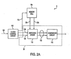
- FIG. 2A shows an AC sensing circuit and other components of the PCRAM device of FIG. 1 in simplified block diagram form
- FIG. 2B is a schematic circuit diagram showing components of FIG. 2A in grater detail
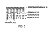
- FIG. 3 is a timing diagram for signals provided by the clock/control circuit in FIG. 2B ;
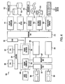
- FIG. 4 shows a digital processing system incorporating a memory device according to an exemplary embodiment of the present invention.
- Resistive memory bits can be modeled as resistors.
- a current is applied to the memory bit and a voltage is measured or a voltage is applied to the memory bit and a current is measured.
- FIG. 1 shows a portion of a PCRAM device including an array 9 of resistive memory cells (memory bits) arranged at the intersection of column lines (bit lines/digit lines) 20a-20d and row lines (word lines) 15a-15d.
- array 9 includes cellplate lines 22a, 22b, 22c and 22d paired respectively with bit lines 20a, 20b, 20c and 20d.
- Memory cell 10a is addressed by row line 156 and digit 20b and cellplate line 22b.
- Memory cell 10b is addressed by row line 15c and line 20b.
- Memory cells 10a and 10b each include an access transistor 25 and a programmable resistance element 30 connected in series between bit line 20b and cellplate line 22b. Bit line 20b and cellplate line 22b are similarly connected to all cells in the same column of array 9.
- the exemplary embodiments of the present invention are described with reference to exemplary memory cell 10a.
- bit lines 20a, 20b, 20c and 20d are each connected to a respective AC sensing circuit 35 and may be implemented as shown in FIGs. 2A and 2B or with other appropriate components.
- Array 9 and the peripheral circuitry could all be integrated in a single integrated circuit, if desired.
- FIG. 2A shows an exemplary embodiment of the AC sensing circuit 35 in simplified block diagram form together with other components of memory device 8.
- AC sensing circuit 35 includes switching circuit 110 and comparison circuit 115.
- Memory device 8 also includes a clock/control circuit 105 coupled to memory element 10a through word line 15b and further coupled to switching circuit 110.
- the memory cell 10a is also coupled to the switching circuit 110 through bit line 20b and cellplate line 22b.
- the clock/control circuit 105 receives a source clock signal 120 and provides a cellplate count signal 135 and a bit count signal 130 to switching circuit 110. Clock/control circuit 105 also provides a signal on word line 15b.
- the signal on word line 15b is received by memory cell 10a and other cells in the same row.
- the signal on each row's word line functions as a control signal to control when the sensing operation is performed for all cells in the row.
- a high pulse on a row's word line turns on transistor 25 of each cell, providing a conductive path through resistance element 30.
- switching circuit 110 In response to signals 130 and 135, switching circuit 110 provides two signals to comparison circuit 115 via two signal lines 122. At any point in time at which a comparison is made between the signal, on lines 125, one signal line 122 is at the supply voltage V cc and the other is at a voltage that depends on resistance element 30. The signal through resistance element 30 alternates polarity during a read operation.
- FIG. 2B shows more detailed exemplary embodiments of the components shown in FIG. 2A .
- the illustrated switching circuit 110 includes PMOS transistors 45, 50 controlled by signals 135, 130, respectively.
- Cellplate line 22b and bit line 20b are each coupled through respective transistors 45, 50 to the supply voltage V cc .
- the clock/control circuit 105 includes cellplate counter 60, bit counter 65, Exclusive-or (XOR) gate 80 and two inverters 70, 75.
- a source clock signal is supplied to cellplate counter 60 and bit line counter 65.
- Cellplate counter 60 provides its output to inverter 70 and XOR gate 80.
- Bit line counter 65 similarly provides its output to inverter 75 and XOR gate 80.
- XOR gate 80 in turn, modulates a signal on word line 15b, to control when transistor 25 is turned on.
- Inverters 70 and 75 provide signals 135 and 130 respectively.
- Comparison circuit 115 includes inverter 85, CMOS multiplexers 90, 95 and switched capacitor sensing amplifier 100.
- Signal 135 from inverter 70 is applied to the gate of transistor 45 and to inverter 85.
- Signal 135 from inverter 70 is also applied as a control signal to each CMOS multiplexer 90, 95 as is the output of inverter 85.
- the output from inverter 75 is applied to the gate of transistor 50. When turned on by signal 135 going low, transistor 45 pulls cellplate line 22b to V cc ; when turned on by signal 130 going low, transistor 50 pulls bit line 20b to V cc .
- Lines 122 connect bit line 20b and cellplate line 22b to both CMOS multiplexers 90, 95.
- the CMOS multiplexers 90, 95 can be conventional four transistor multiplexers, each multiplexer having five terminals (two input terminals, two control terminals and one output terminal).
- the CMOS multiplexers 90, 95 will each select one input from lines 122 as its output based on signal 135 and the output of inverter 75.
- CMOS multiplexer (MUX) 95 provides the signal from bit line 20b while MUX 90 provides V cc from transistor 45; when signal 135 is high, MUX 90 provides V cc from transistor 50 and MUX 95 provides the signal from cellplate 22b.
- MUX 95 always provides a sensed signal from memory cell 10a while MUX 90 always provides V cc as a reference voltage.
- Switched capacitor sensing amplifier 100 is a current input amplifier that is sensitive to a small amount of positive or negative current at its terminals and compares the current with a threshold. The threshold is set so that the output of the switched capacitor sensing amplifier 100 corresponds to the logic state of a particular memory cell connected to bit line 20b and cellplate line 22b, such as memory cell 10a. There is one switched capacitor sensing amplifier 100 per column or bit line but only one row of cells is read at one time under control of the word lines.
- FIGs. 2A and 2B depict a single cell only.
- a memory device has a plurality of memory elements arranged in rows and columns.
- the circuit of the present invention is intended to be adapted for a memory device.
- a single control circuit is used for each column with additional selection logic and access devices (not shown). That is, the XOR gate is an "enabled" XOR gate being enabled by word line decode circuitry.
- Multiple counters are advantageously stacked in the row direction with one set of counters for each column or one set of counters per chip. Similarly, one comparison circuit per column would be advantageous.
- the switching circuit would advantageously have additional multiplexers for use with a memory device.
- FIG. 3 is a timing diagram for signals from circuit 105 in FIG. 2B .
- Transistor 25 is on when the signal on word line 15b goes high. In the first instance that the word line 15b goes high, cellplate count signal 135 is high and bit count signal 130 is low. In the next instance that the word line 15b goes high, the cellplate count signal 135 is low and bit count signal 130 is high. The read cycles thus alternate in the direction of the current through resistance 30.
- Comparison circuit 115 effectively rectifies the alternating current before switched capacitor sensing amplifier 100 provides the output bit.
- bit count signal and the cellplate count signal is 6:2 or 3:1 and that there are four clock transitions (rising and falling edges) of the bit count signal 130 for each pair of transitions (rising and falling edge) of the cellplate count signal 135. That is, the cellplate count signal 135 is the (input) clock signal divided by 6 and the bit count signal 130 is the clock signal divided by 2.
- XOR gate 80 ( FIG. 2B ) ensures that the signal on word line signal 15b is high when the cellplate count signal 135 is high and the bit count signal 130 is low or when the cellplate count signal 135 is low and the bit count signal 130 is high.
- signal 135 is low and word line 15b is high, current flows from transistor 45 through resistive element 30 and CMOS multiplexer 95 to switched capacitor sensing amplifier 100.
- signal 130 is low and word line 15b is high, current flows from transistor 50 through resistive element 30 and CMOS multiplexer 90 to switched capacitor sensing amplifier 100.
- the present invention has been described using PMOS transistors but may also be implemented using NMOS transistors.
- the control signals are described as clock signals with which the cellplate line and bit line have a certain relationship one to the other. These control signals may be of any other form or relationship so long as they function as described herein to control memory cells and to gate transistors in the switching circuit.
- the control circuit, switching circuit and comparison circuits of the present invention may be implemented with individual components moved to another circuit so long as the requisite functionality is implemented.
- the inverters of the control circuit may be considered part of the switching circuit.
- the inverters and multiplexers of the comparison circuit may also be considered part of the switching circuit.
- FIG. 4 illustrates an exemplary digital processing system 500 which has components 508 utilizing a memory device 8 employing the sensing circuit 35 of the present invention disclosed above in connection with FIGs. 1-3 .
- the processing system 500 includes one or more processors 501 coupled to a local bus 504.
- a memory controller 502 and a primary bus bridge 503 are also coupled to the local bus 504.
- the processing system 500 may include multiple memory controllers 502 and/or multiple primary bus bridges 503.
- the memory controller 502 and the primary bus bridge 503 may be integrated as a single device 506.
- the memory controller 502 is also coupled to one or more memory buses 507. Each memory bus accepts memory components 508, which include at least one memory device 8 that includes sensing circuit 35. Each of the memory components 508 may be a memory card or a memory module. Examples of memory modules include single inline memory modules (SIMMs) and dual inline memory modules (DIMMs). The memory components 508 may include one or more additional devices.
- the memory controller 502 may also be coupled to a cache memory 505.
- the cache memory 505 may be the only cache memory in the processing system. Alternatively, other devices, for example, processors 501 may also include cache memories, which may form a cache hierarchy with cache memory 505.
- the memory controller 502 may implement a cache coherency protocol. If the memory controller 502 is coupled to a plurality of memory buses 507, each memory bus 507 may be operated in parallel, or different address ranges may be mapped to different memory buses 507.
- DMA direct memory access
- the primary bus bridge 503 is coupled to at least one peripheral bus 510.
- Various devices such as peripherals or additional bus bridges may be coupled to the peripheral bus 510. These devices may include a storage controller 511, a miscellaneous I/O device 514, a secondary bus bridge 515, a multimedia processor 518, and a legacy device interface 520.
- the primary bus bridge 503 may also coupled to one or more special purpose high speed ports 522. In a personal computer, for example, the special purpose port might be the Accelerated Graphics Port (AGP), used to couple a high performance video card to the processing system 500.
- AGP Accelerated Graphics Port
- the storage controller 511 couples one or more storage devices 513, via a storage bus 512, to the peripheral bus 510.
- the storage controller 511 may be a SCSI controller and storage devices 513 may be SCSI discs.
- the I/O device 514 may be any sort of peripheral.
- the I/O device 514 may be a local area network interface, such as an Ethernet card.
- the secondary bus bridge may be used to interface additional devices via another bus to the processing system.
- the secondary bus bridge may be an universal serial port (USB) controller used to couple USB devices 517 via to the processing system 500.
- the multimedia processor 518 may be a sound card, a video capture card, or any other type of media interface, which may also be coupled to one additional devices such as speakers 519.
- the legacy device interface 520 is used to couple legacy devices 521, for example, older styled keyboards and mice, to the processing system 500.
- the processing system 500 illustrated in FIG. 4 is only an exemplary processing system with which the invention may be used. While FIG. 4 illustrates a processing architecture especially suitable for a general purpose computer, such as a personal computer or a workstation, it should be recognized that well known modifications can be made to configure the processing system 500 to become more suitable for use in a variety of applications. For example, many electronic devices that require processing may be implemented using a simpler architecture that relies on a CPU 501 coupled to memory components 508. These electronic devices may include, but are not limited to audio/video processors and recorders, gaming consoles, digital television sets, wired or wireless telephones, navigation devices (including systems based on the global positioning system (GPS) and/or inertial navigation), and digital cameras and/or recorders. The modifications may include, for example, elimination of unnecessary components, addition of specialized devices or circuits, and/or integration of a plurality of devices.
- GPS global positioning system
Landscapes
- Engineering & Computer Science (AREA)
- Computer Hardware Design (AREA)
- Semiconductor Memories (AREA)
- Dram (AREA)
- Static Random-Access Memory (AREA)
- For Increasing The Reliability Of Semiconductor Memories (AREA)
- Read Only Memory (AREA)
Abstract
Description
- The present invention relates to resistive memory devices and, more particularly, to read/sense circuitry for programmable contact random access memory (PCRAM) devices.
- Integrated circuit designers have always sought the ideal semiconductor memory -- a device that is randomly accessible, can be written and read very quickly, is non-volatile, but indefinitely alterable, and consumes little power. Programmable contact random access memory (PCRAM) technology has been increasingly viewed as offering all these advantages.
- Digital memories are widely used in computers, computer system components and computer processing systems. Resistive memories store digital information in the form of bits or binary digits as "0"s or "1"s based on the resistance of a memory element or cell. Resistive memory devices are configured in arrays where a resistive element or cell is at the intersection of a row line (word line) and a column line (digit line or bit line). In order to read or sense the state of a memory cell, it is necessary to first select the desired memory cell by selecting the column line and row line, which intersect at the desired memory element. Once the desired memory element is isolated, the selected memory cell is then read by applying a read voltage to the cell to detect the resistance of the memory cell and thereby, determine the logic state of the memory cell.
- For binary logic state sensing, the absolute magnitude of memory cell resistance need not be known, only whether the resistance of a memory cell is above or below a threshold value that is between logic one and logic zero resistance values. Nonetheless, sensing the logic state of a PCRAM memory element is difficult because the technology of the PCRAM device imposes multiple constraints.
- The present invention provides embodiments in which the state of a resistive memory element is read using an alternating current (AC). Reading the state of a resistive memory element with AC avoids over-programming or erasing the memory element.
- These and other features and advantages of the invention will be more clearly understood from the following detailed description, which is provided in connection with the accompanying drawings, in which:
-
FIG. 1 shows a portion of a programmable contact random access memory (PCRAM) device; -
FIG. 2A shows an AC sensing circuit and other components of the PCRAM device ofFIG. 1 in simplified block diagram form; -
FIG. 2B is a schematic circuit diagram showing components ofFIG. 2A in grater detail; -
FIG. 3 is a timing diagram for signals provided by the clock/control circuit inFIG. 2B ; and -
FIG. 4 shows a digital processing system incorporating a memory device according to an exemplary embodiment of the present invention. - Memory bits based on changes in the resistance of materials in response to a programming (writing or erasing) voltage or current hold a great deal of promise for non-volatile memories. Some of these resistive memory bits (mbits) exhibit changes in viability if read repeatedly due to a small current being applied repeatedly to sense/read the device. As it loses viability, the memory bit is not so easily programmed or erased and may even remain in a logic state.
- Resistive memory bits can be modeled as resistors. In a conventional direct current (DC) reading/sensing circuit, a current is applied to the memory bit and a voltage is measured or a voltage is applied to the memory bit and a current is measured.
-
FIG. 1 shows a portion of a PCRAM device including an array 9 of resistive memory cells (memory bits) arranged at the intersection of column lines (bit lines/digit lines) 20a-20d and row lines (word lines) 15a-15d. In addition, array 9 includescellplate lines bit lines - Two
exemplary memory cells Memory cell 10a is addressed by row line 156 anddigit 20b andcellplate line 22b.Memory cell 10b is addressed byrow line 15c andline 20b.Memory cells access transistor 25 and aprogrammable resistance element 30 connected in series betweenbit line 20b andcellplate line 22b.Bit line 20b andcellplate line 22b are similarly connected to all cells in the same column of array 9. In the following discussion, the exemplary embodiments of the present invention are described with reference toexemplary memory cell 10a. - In accordance with an exemplary embodiment the present invention,
bit lines AC sensing circuit 35 and may be implemented as shown inFIGs. 2A and2B or with other appropriate components. Array 9 and the peripheral circuitry could all be integrated in a single integrated circuit, if desired. -
FIG. 2A shows an exemplary embodiment of theAC sensing circuit 35 in simplified block diagram form together with other components ofmemory device 8.AC sensing circuit 35 includesswitching circuit 110 andcomparison circuit 115.Memory device 8 also includes a clock/control circuit 105 coupled tomemory element 10a throughword line 15b and further coupled to switchingcircuit 110. Thememory cell 10a is also coupled to theswitching circuit 110 throughbit line 20b andcellplate line 22b. - The clock/
control circuit 105 receives asource clock signal 120 and provides acellplate count signal 135 and abit count signal 130 to switchingcircuit 110. Clock/control circuit 105 also provides a signal onword line 15b. - The signal on
word line 15b is received bymemory cell 10a and other cells in the same row. The signal on each row's word line functions as a control signal to control when the sensing operation is performed for all cells in the row. A high pulse on a row's word line turns ontransistor 25 of each cell, providing a conductive path throughresistance element 30. - In response to
signals switching circuit 110 provides two signals tocomparison circuit 115 via twosignal lines 122. At any point in time at which a comparison is made between the signal, on lines 125, onesignal line 122 is at the supply voltage Vcc and the other is at a voltage that depends onresistance element 30. The signal throughresistance element 30 alternates polarity during a read operation. -
FIG. 2B shows more detailed exemplary embodiments of the components shown inFIG. 2A . The illustratedswitching circuit 110 includesPMOS transistors signals Cellplate line 22b andbit line 20b are each coupled throughrespective transistors - The clock/
control circuit 105 includescellplate counter 60,bit counter 65, Exclusive-or (XOR)gate 80 and twoinverters cellplate counter 60 andbit line counter 65.Cellplate counter 60 provides its output to inverter 70 and XORgate 80.Bit line counter 65 similarly provides its output to inverter 75 andXOR gate 80.XOR gate 80, in turn, modulates a signal onword line 15b, to control whentransistor 25 is turned on.Inverters signals -
Comparison circuit 115 includesinverter 85,CMOS multiplexers capacitor sensing amplifier 100.Signal 135 frominverter 70 is applied to the gate oftransistor 45 and toinverter 85.Signal 135 frominverter 70 is also applied as a control signal to eachCMOS multiplexer inverter 85. The output frominverter 75 is applied to the gate oftransistor 50. When turned on bysignal 135 going low,transistor 45 pullscellplate line 22b to Vcc; when turned on bysignal 130 going low,transistor 50 pullsbit line 20b to Vcc. -
Lines 122connect bit line 20b andcellplate line 22b to bothCMOS multiplexers lines 122 as its output based onsignal 135 and the output ofinverter 75. When signal 135 is low, CMOS multiplexer (MUX) 95 provides the signal frombit line 20b whileMUX 90 provides Vcc fromtransistor 45; whensignal 135 is high,MUX 90 provides Vcc fromtransistor 50 andMUX 95 provides the signal fromcellplate 22b. As a result,MUX 95 always provides a sensed signal frommemory cell 10a whileMUX 90 always provides Vcc as a reference voltage. - The outputs of the
CMOS multiplexers capacitor sensing amplifier 100. Switchedcapacitor sensing amplifier 100 is a current input amplifier that is sensitive to a small amount of positive or negative current at its terminals and compares the current with a threshold. The threshold is set so that the output of the switchedcapacitor sensing amplifier 100 corresponds to the logic state of a particular memory cell connected to bitline 20b andcellplate line 22b, such asmemory cell 10a. There is one switchedcapacitor sensing amplifier 100 per column or bit line but only one row of cells is read at one time under control of the word lines. -
FIGs. 2A and2B depict a single cell only. A memory device has a plurality of memory elements arranged in rows and columns. The circuit of the present invention is intended to be adapted for a memory device. When adapted for use with a memory device, a single control circuit is used for each column with additional selection logic and access devices (not shown). That is, the XOR gate is an "enabled" XOR gate being enabled by word line decode circuitry. Multiple counters are advantageously stacked in the row direction with one set of counters for each column or one set of counters per chip. Similarly, one comparison circuit per column would be advantageous. The switching circuit would advantageously have additional multiplexers for use with a memory device. -
FIG. 3 is a timing diagram for signals fromcircuit 105 inFIG. 2B .Transistor 25 is on when the signal onword line 15b goes high. In the first instance that theword line 15b goes high,cellplate count signal 135 is high and bit countsignal 130 is low. In the next instance that theword line 15b goes high, thecellplate count signal 135 is low and bit countsignal 130 is high. The read cycles thus alternate in the direction of the current throughresistance 30.Comparison circuit 115, however, effectively rectifies the alternating current before switchedcapacitor sensing amplifier 100 provides the output bit. It should be understood that the relationship between the bit count signal and the cellplate count signal is 6:2 or 3:1 and that there are four clock transitions (rising and falling edges) of thebit count signal 130 for each pair of transitions (rising and falling edge) of thecellplate count signal 135. That is, thecellplate count signal 135 is the (input) clock signal divided by 6 and thebit count signal 130 is the clock signal divided by 2. - XOR gate 80 (
FIG. 2B ) ensures that the signal onword line signal 15b is high when thecellplate count signal 135 is high and thebit count signal 130 is low or when thecellplate count signal 135 is low and thebit count signal 130 is high. When signal 135 is low andword line 15b is high, current flows fromtransistor 45 throughresistive element 30 andCMOS multiplexer 95 to switchedcapacitor sensing amplifier 100. When signal 130 is low andword line 15b is high, current flows fromtransistor 50 throughresistive element 30 andCMOS multiplexer 90 to switchedcapacitor sensing amplifier 100. - Among the advantages of employing AC sensing for resistive memory cells is prolonging the viability of the memory cells of a memory device. Reading the state of a memory element/cell with AC avoids over-programming or partially erasing the memory element.
- The present invention has been described using PMOS transistors but may also be implemented using NMOS transistors. The control signals are described as clock signals with which the cellplate line and bit line have a certain relationship one to the other. These control signals may be of any other form or relationship so long as they function as described herein to control memory cells and to gate transistors in the switching circuit. The control circuit, switching circuit and comparison circuits of the present invention may be implemented with individual components moved to another circuit so long as the requisite functionality is implemented. For example, the inverters of the control circuit may be considered part of the switching circuit. The inverters and multiplexers of the comparison circuit may also be considered part of the switching circuit.
-
FIG. 4 illustrates an exemplarydigital processing system 500 which hascomponents 508 utilizing amemory device 8 employing thesensing circuit 35 of the present invention disclosed above in connection withFIGs. 1-3 . Theprocessing system 500 includes one ormore processors 501 coupled to alocal bus 504. Amemory controller 502 and aprimary bus bridge 503 are also coupled to thelocal bus 504. Theprocessing system 500 may includemultiple memory controllers 502 and/or multiple primary bus bridges 503. Thememory controller 502 and theprimary bus bridge 503 may be integrated as asingle device 506. - The
memory controller 502 is also coupled to one ormore memory buses 507. Each memory bus acceptsmemory components 508, which include at least onememory device 8 that includessensing circuit 35. Each of thememory components 508 may be a memory card or a memory module. Examples of memory modules include single inline memory modules (SIMMs) and dual inline memory modules (DIMMs). Thememory components 508 may include one or more additional devices. Thememory controller 502 may also be coupled to a cache memory 505. The cache memory 505 may be the only cache memory in the processing system. Alternatively, other devices, for example,processors 501 may also include cache memories, which may form a cache hierarchy with cache memory 505. If theprocessing system 500 includes peripherals or controllers which are bus masters or which support direct memory access (DMA), thememory controller 502 may implement a cache coherency protocol. If thememory controller 502 is coupled to a plurality ofmemory buses 507, eachmemory bus 507 may be operated in parallel, or different address ranges may be mapped todifferent memory buses 507. - The
primary bus bridge 503 is coupled to at least oneperipheral bus 510. Various devices, such as peripherals or additional bus bridges may be coupled to theperipheral bus 510. These devices may include astorage controller 511, a miscellaneous I/O device 514, asecondary bus bridge 515, amultimedia processor 518, and alegacy device interface 520. Theprimary bus bridge 503 may also coupled to one or more special purpose high speed ports 522. In a personal computer, for example, the special purpose port might be the Accelerated Graphics Port (AGP), used to couple a high performance video card to theprocessing system 500. - The
storage controller 511 couples one ormore storage devices 513, via astorage bus 512, to theperipheral bus 510. For example, thestorage controller 511 may be a SCSI controller andstorage devices 513 may be SCSI discs. The I/O device 514 may be any sort of peripheral. For example, the I/O device 514 may be a local area network interface, such as an Ethernet card. The secondary bus bridge may be used to interface additional devices via another bus to the processing system. For example, the secondary bus bridge may be an universal serial port (USB) controller used to coupleUSB devices 517 via to theprocessing system 500. Themultimedia processor 518 may be a sound card, a video capture card, or any other type of media interface, which may also be coupled to one additional devices such asspeakers 519. Thelegacy device interface 520 is used to couplelegacy devices 521, for example, older styled keyboards and mice, to theprocessing system 500. - The
processing system 500 illustrated inFIG. 4 is only an exemplary processing system with which the invention may be used. WhileFIG. 4 illustrates a processing architecture especially suitable for a general purpose computer, such as a personal computer or a workstation, it should be recognized that well known modifications can be made to configure theprocessing system 500 to become more suitable for use in a variety of applications. For example, many electronic devices that require processing may be implemented using a simpler architecture that relies on aCPU 501 coupled tomemory components 508. These electronic devices may include, but are not limited to audio/video processors and recorders, gaming consoles, digital television sets, wired or wireless telephones, navigation devices (including systems based on the global positioning system (GPS) and/or inertial navigation), and digital cameras and/or recorders. The modifications may include, for example, elimination of unnecessary components, addition of specialized devices or circuits, and/or integration of a plurality of devices. - While embodiments of the invention have been described in the illustrations above, it should be understood that these are exemplary of the invention and are not to be considered as limiting. While the present invention has been described in terms of PCRAM, it is not limited thereto but is applicable to, for example, magnetic resistive random access memory (MRAM) PCRAM and other circuits in which signals are sensed at different levels. Additions, deletions, substitutions, and other modifications can be made without departing from the spirit or scope of the present invention. Accordingly, the invention is not to be considered as limited by the foregoing description but is only limited by the scope of the appended claims.
- Further aspects of the present invention may be defined by the following clauses:
- 1. An apparatus for sensing a logic state of a memory cell, comprising: a control circuit providing a control signal to said memory cell, said control signal controlling when said memory cell is sensed; a switching circuit that receives a cellplate count signal and a bit count signal provided by said control circuit, said switching circuit further receiving a cellplate line signal and a bit line signal from said memory cell, said switching circuit producing a first output signal and a second output signal, wherein one of said first output signal and said second output signal is at a supply voltage and the other of said first output signal and said second output signal alternates polarity with each sensing operation; and a comparison circuit receiving said first and second output signals and outputting a signal corresponding to the logic state of said memory cell.
- 2. The apparatus according to
clause 1, wherein said control circuit comprises: a cellplate counter that produces said cellplate count signal; a digit counter that produces said bit count signal; and an exclusive-or (XOR) gate that produces said control signal. - 3. The apparatus according to
clause 2, wherein said control circuit comprises: a first inverter for receiving said cellplate count and producing an inverted cellplate count signal and applying said inverted cellplate count signal to said switching circuit; and a second inverter for receiving said bit count signal and producing an inverted bit count signal and applying said inverted bit count signal to said switching circuit. - 4. The apparatus according to
clause 3, wherein said comparison circuit further comprises: a third inverter for receiving said inverted cellplate count signal and producing an inverted signal; a first multiplexer for receiving said inverted signal, said inverted cellplate count signal, said first output signal, and said second output signal, said first multiplexer producing a third output signal; a second multiplexer for receiving said inverted signal, said inverted cellplate count signal, said first output signal, and said second output signal, said second multiplexer producing a fourth output signal; and a switched capacitor sensing amplifier for selecting one of said first output signal and said second output signal, said selected one of said first output signal and said second output signal corresponding to said logic state of said memory cell. - 5. The apparatus according to
clause 1, wherein said comparison circuit comprises a switched capacitor sensing amplifier for selecting one of said first output signal and said second output signal, said selected one of said first output signal and said second output signal corresponding to the logic state of said memory cell. - 6. The apparatus according to
clause 1, wherein said switching circuit comprises: a first inverter for receiving said cellplate count and producing an inverted cellplate count signal and applying said inverted cellplate count signal to said switching circuit; a second inverter for receiving said bit count signal and producing an inverted bit count signal and applying said inverted bit count signal to said switching circuit. a third inverter for receiving said inverted cellplate count signal and producing an inverted signal; a first multiplexer for receiving said inverted signal, said inverted cellplate count signal, said first output signal, and said second output signal, said first multiplexer producing a third output signal; and a second multiplexer for receiving said inverted signal, said inverted cellplate count signal, said first output signal, and said second output signal, said second multiplexer producing a fourth output signal. - 7. A processing system, comprising: a processor; and a memory device coupled to said processor via a bus, said memory device comprising: an array of memory cells, a cellplate line common across said array of memory cells, and an apparatus for sensing a logic state of a memory cell, comprising: a control circuit providing a control signal, said control signal controlling when said memory cell is sensed; a switching circuit that receives a cellplate count signal and a bit count signal provided by said control circuit, said switching circuit further receiving a cellplate line signal and a bit line signal from said memory cell, said switching circuit producing a first output signal and a second output signal, wherein one of said first output signal and said second output signal is at a supply voltage and the other of said first output signal and said second output signal alternates polarity with each sensing operation; and a comparison circuit receiving said first and second output signals and outputting a signal corresponding to the logic state of said memory cell.
Claims (11)
- A resistive memory cell (10a, 10b) comprising:a memory element (30) having at least two resistive states; anda first connection and a second connection to first and second sensing lines respectively, said memory element (30) being connected in series between said first connection and said second connection and capable of conducting sensing current alternately from said first sensing line to said second sensing line and from said second sensing line to said first sensing line.
- The resistive memory cell (10a, 10b) according to claim 1, wherein said memory element (30) is a programmable contact random access memory (PCRAM) element.
- The resistive memory cell (10a, 10b) according to claim 1, further comprising a switching element (25) connected in series with said memory element (30) that controls sensing of said memory element (30).
- A sensing circuit for resistive memory cells (10a, 10b), comprising:first and second sensing lines between which are connected a memory element (30) having at least two resistive memory states;switching circuitry that provides sensing current through the memory element (30) alternately from said first sensing line to said second sensing line and from said second sensing line to said first sensing line; andoutput circuitry that receives said sensing current and, in response, provides an output signal indicating a resistance state of said memory element (30).
- A memory device comprising:an array of memory cells (10a, 10b);a cellplate line common across said array of memory cells (10a, 10b); andthe sensing circuit for resistive memory cells of claim 4.
- A processing system, comprising:a processor; anda memory device coupled to said processor via a bus, said memory device comprising:an array of memory cells (10a, 10b),a cellplate line common across said array of memory cells (10a, 10b), and the sensing circuit for resistive memory cells of claim 4.
- An integrated circuit comprising: a memory device, said memory device comprising:an array of memory cells (10a, 10b),a cellplate line common across said array of memory cells (10a, 10b), andthe sensing circuit for resistive memory cells of claim 4.
- A method of sensing a resistive state of a resistive memory element (30), said method comprising:providing sensing current alternately in a first direction and a second opposite direction through said memory element (30); andin response to said sensing current, providing an output signal indicating a resistance state of said memory element (30).
- A method for sensing a logic state of a memory cell (10a, 10b), said method comprising:receiving a clock signal from a clock source;producing a cellplate count signal (135);producing an inverted cellplate count signal; andapplying said cellplate count signal (135), said inverted cellplate count signal, a first signal based on a cellplate line of said memory cell, a second signal based on a bit line of said memory cell to a comparison circuit to produce a signal corresponding to said logic state of said memory cell.
- The method according to claim 9, further comprising:producing a bit count signal (130); andproducing a control signal based on said cellplate count and said digit count, said control signal applied to said memory cell to control when sensing occurs.
- The method according to claim 10, further comprising:producing an inverted bit count signal;applying said inverted cellplate count signal to a gate of a first transistor, said first transistor coupled to said cellplate line of said memory cell (10a, 10b);applying said inverted bit count signal to a gate of a second transistor, said second transistor coupled to said bit line of said memory cell (10a, 10b);producing said first signal; andproducing said second signal.
Applications Claiming Priority (2)
| Application Number | Priority Date | Filing Date | Title |
|---|---|---|---|
| US10/681,161 US7123530B2 (en) | 2003-10-09 | 2003-10-09 | AC sensing for a resistive memory |
| EP04794289A EP1673780B1 (en) | 2003-10-09 | 2004-10-06 | Ac sensing for a resistive memory |
Related Parent Applications (2)
| Application Number | Title | Priority Date | Filing Date |
|---|---|---|---|
| EP04794289.1 Division | 2004-10-06 | ||
| EP04794289A Division EP1673780B1 (en) | 2003-10-09 | 2004-10-06 | Ac sensing for a resistive memory |
Publications (3)
| Publication Number | Publication Date |
|---|---|
| EP2026353A2 true EP2026353A2 (en) | 2009-02-18 |
| EP2026353A3 EP2026353A3 (en) | 2009-06-03 |
| EP2026353B1 EP2026353B1 (en) | 2011-06-15 |
Family
ID=34422239
Family Applications (2)
| Application Number | Title | Priority Date | Filing Date |
|---|---|---|---|
| EP08019815A Expired - Lifetime EP2026353B1 (en) | 2003-10-09 | 2004-10-06 | AC sensing for a resistive memory |
| EP04794289A Expired - Lifetime EP1673780B1 (en) | 2003-10-09 | 2004-10-06 | Ac sensing for a resistive memory |
Family Applications After (1)
| Application Number | Title | Priority Date | Filing Date |
|---|---|---|---|
| EP04794289A Expired - Lifetime EP1673780B1 (en) | 2003-10-09 | 2004-10-06 | Ac sensing for a resistive memory |
Country Status (8)
| Country | Link |
|---|---|
| US (2) | US7123530B2 (en) |
| EP (2) | EP2026353B1 (en) |
| JP (1) | JP4620676B2 (en) |
| KR (2) | KR100815368B1 (en) |
| CN (2) | CN102394095B (en) |
| AT (2) | ATE513294T1 (en) |
| TW (1) | TWI252493B (en) |
| WO (1) | WO2005036557A2 (en) |
Families Citing this family (15)
| Publication number | Priority date | Publication date | Assignee | Title |
|---|---|---|---|---|
| US7123530B2 (en) * | 2003-10-09 | 2006-10-17 | Micron Technology, Inc. | AC sensing for a resistive memory |
| JP2007080311A (en) * | 2005-09-12 | 2007-03-29 | Sony Corp | Memory device and semiconductor device |
| US7271011B2 (en) * | 2005-10-28 | 2007-09-18 | Freescale Semiconductor, Inc. | Methods of implementing magnetic tunnel junction current sensors |
| US7397689B2 (en) * | 2006-08-09 | 2008-07-08 | Micron Technology, Inc. | Resistive memory device |
| US20080310210A1 (en) * | 2007-06-13 | 2008-12-18 | Dietmar Gogl | Semiconductor memory device and method of operation |
| US7881100B2 (en) * | 2008-04-08 | 2011-02-01 | Micron Technology, Inc. | State machine sensing of memory cells |
| US7835173B2 (en) * | 2008-10-31 | 2010-11-16 | Micron Technology, Inc. | Resistive memory |
| US7929338B2 (en) * | 2009-02-24 | 2011-04-19 | International Business Machines Corporation | Memory reading method for resistance drift mitigation |
| US8208291B2 (en) * | 2010-01-14 | 2012-06-26 | Qualcomm Incorporated | System and method to control a direction of a current applied to a magnetic tunnel junction |
| US8817530B2 (en) | 2011-11-17 | 2014-08-26 | Everspin Technologies, Inc. | Data-masked analog and digital read for resistive memories |
| TWI539457B (en) * | 2014-11-26 | 2016-06-21 | 華邦電子股份有限公司 | Resistive random access memory and manufacturing method thereof |
| CN105788631B (en) * | 2014-12-15 | 2019-01-04 | 华邦电子股份有限公司 | Resistive random access memory with and preparation method thereof |
| KR102431206B1 (en) * | 2015-12-23 | 2022-08-11 | 에스케이하이닉스 주식회사 | Electronic device |
| US9799381B1 (en) * | 2016-09-28 | 2017-10-24 | Intel Corporation | Double-polarity memory read |
| JP2019057582A (en) * | 2017-09-20 | 2019-04-11 | 東芝メモリ株式会社 | Memory device and variable resistance element |
Family Cites Families (16)
| Publication number | Priority date | Publication date | Assignee | Title |
|---|---|---|---|---|
| JP3001657B2 (en) * | 1991-03-01 | 2000-01-24 | 富士通株式会社 | Semiconductor storage device |
| JP3151123B2 (en) * | 1995-04-24 | 2001-04-03 | シャープ株式会社 | Nonvolatile semiconductor memory device |
| TW324101B (en) * | 1995-12-21 | 1998-01-01 | Hitachi Ltd | Semiconductor integrated circuit and its working method |
| KR100232895B1 (en) * | 1996-12-31 | 1999-12-01 | 김영환 | Sense amp. enable signal generating apparatus |
| KR100301367B1 (en) * | 1998-07-25 | 2001-10-27 | 윤종용 | Synchronous Semiconductor Memory Device with Sense Amplifier Control |
| US6111781A (en) * | 1998-08-03 | 2000-08-29 | Motorola, Inc. | Magnetic random access memory array divided into a plurality of memory banks |
| US6462998B1 (en) * | 1999-02-13 | 2002-10-08 | Integrated Device Technology, Inc. | Programmable and electrically configurable latch timing circuit |
| DE19950581A1 (en) * | 1999-10-20 | 2001-04-26 | Infineon Technologies Ag | Arrangement for self-referencing ferroelectric memory cells |
| JP3985432B2 (en) * | 2000-06-19 | 2007-10-03 | 日本電気株式会社 | Magnetic random access memory |
| KR100355235B1 (en) * | 2000-07-18 | 2002-10-11 | 삼성전자 주식회사 | Semiconductor memory device adjusting sensing gain of data line sense amplifier |
| DE10149737A1 (en) * | 2001-10-09 | 2003-04-24 | Infineon Technologies Ag | Semiconductor memory with magnetoresistive memory cells having 2 magnetic layers of hard and soft ferromagnetic materials separated by insulation layer |
| US6791859B2 (en) * | 2001-11-20 | 2004-09-14 | Micron Technology, Inc. | Complementary bit PCRAM sense amplifier and method of operation |
| US6804145B2 (en) * | 2002-11-01 | 2004-10-12 | Hewlett-Packard Development Company, L.P. | Memory cell sensing system and method |
| CN1444296A (en) * | 2003-04-15 | 2003-09-24 | 山东大学 | Giant magneto-impedance effect composite wire and its preparation method |
| US6795359B1 (en) * | 2003-06-10 | 2004-09-21 | Micron Technology, Inc. | Methods and apparatus for measuring current as in sensing a memory cell |
| US7123530B2 (en) * | 2003-10-09 | 2006-10-17 | Micron Technology, Inc. | AC sensing for a resistive memory |
-
2003
- 2003-10-09 US US10/681,161 patent/US7123530B2/en not_active Expired - Lifetime
-
2004
- 2004-10-06 EP EP08019815A patent/EP2026353B1/en not_active Expired - Lifetime
- 2004-10-06 AT AT04794289T patent/ATE513294T1/en not_active IP Right Cessation
- 2004-10-06 JP JP2006534276A patent/JP4620676B2/en not_active Expired - Fee Related
- 2004-10-06 KR KR1020067008879A patent/KR100815368B1/en not_active Expired - Lifetime
- 2004-10-06 WO PCT/US2004/032884 patent/WO2005036557A2/en not_active Ceased
- 2004-10-06 EP EP04794289A patent/EP1673780B1/en not_active Expired - Lifetime
- 2004-10-06 CN CN201110340453.5A patent/CN102394095B/en not_active Expired - Lifetime
- 2004-10-06 AT AT08019815T patent/ATE513295T1/en not_active IP Right Cessation
- 2004-10-06 CN CN2004800358887A patent/CN1890752B/en not_active Expired - Lifetime
- 2004-10-06 KR KR1020077014783A patent/KR100890374B1/en not_active Expired - Lifetime
- 2004-10-08 TW TW093130590A patent/TWI252493B/en not_active IP Right Cessation
-
2006
- 2006-07-07 US US11/481,957 patent/US7263017B2/en not_active Expired - Lifetime
Also Published As
| Publication number | Publication date |
|---|---|
| ATE513294T1 (en) | 2011-07-15 |
| KR100815368B1 (en) | 2008-03-19 |
| KR100890374B1 (en) | 2009-03-25 |
| JP4620676B2 (en) | 2011-01-26 |
| EP1673780A2 (en) | 2006-06-28 |
| US7123530B2 (en) | 2006-10-17 |
| TW200529243A (en) | 2005-09-01 |
| EP2026353A3 (en) | 2009-06-03 |
| ATE513295T1 (en) | 2011-07-15 |
| CN102394095A (en) | 2012-03-28 |
| EP2026353B1 (en) | 2011-06-15 |
| JP2007508650A (en) | 2007-04-05 |
| US20050078505A1 (en) | 2005-04-14 |
| WO2005036557A3 (en) | 2005-08-04 |
| US7263017B2 (en) | 2007-08-28 |
| US20060250872A1 (en) | 2006-11-09 |
| KR20070086759A (en) | 2007-08-27 |
| TWI252493B (en) | 2006-04-01 |
| CN1890752A (en) | 2007-01-03 |
| KR20060086395A (en) | 2006-07-31 |
| CN1890752B (en) | 2012-04-25 |
| WO2005036557A2 (en) | 2005-04-21 |
| CN102394095B (en) | 2015-08-12 |
| EP1673780B1 (en) | 2011-06-15 |
Similar Documents
| Publication | Publication Date | Title |
|---|---|---|
| US8611136B2 (en) | Method and apparatus providing a cross-point memory array using a variable resistance memory cell and capacitance | |
| EP1642298B1 (en) | Method for reducing power consumption when sensing a resistive memory | |
| KR100747734B1 (en) | Integrated charge sensing scheme for resistive memories | |
| EP2026353B1 (en) | AC sensing for a resistive memory | |
| US8320179B2 (en) | Dual ported non volatile FIFO with third dimension memory | |
| EP2045817A1 (en) | Methods and apparatus for measuring current as In sensing a memory cell | |
| US7151689B2 (en) | Adjusting the frequency of an oscillator for use in a resistive sense amp | |
| EP1623429B1 (en) | Skewed sense amp for variable resistance memory sensing |
Legal Events
| Date | Code | Title | Description |
|---|---|---|---|
| PUAI | Public reference made under article 153(3) epc to a published international application that has entered the european phase |
Free format text: ORIGINAL CODE: 0009012 |
|
| 17P | Request for examination filed |
Effective date: 20081120 |
|
| AC | Divisional application: reference to earlier application |
Ref document number: 1673780 Country of ref document: EP Kind code of ref document: P |
|
| AK | Designated contracting states |
Kind code of ref document: A2 Designated state(s): AT BE BG CH CY CZ DE DK EE ES FI FR GB GR HU IE IT LI LU MC NL PL PT RO SE SI SK TR |
|
| PUAL | Search report despatched |
Free format text: ORIGINAL CODE: 0009013 |
|
| AK | Designated contracting states |
Kind code of ref document: A3 Designated state(s): AT BE BG CH CY CZ DE DK EE ES FI FR GB GR HU IE IT LI LU MC NL PL PT RO SE SI SK TR |
|
| 17Q | First examination report despatched |
Effective date: 20090821 |
|
| AKX | Designation fees paid |
Designated state(s): AT BE BG CH CY CZ DE DK EE ES FI FR GB GR HU IE IT LI LU MC NL PL PT RO SE SI SK TR |
|
| GRAP | Despatch of communication of intention to grant a patent |
Free format text: ORIGINAL CODE: EPIDOSNIGR1 |
|
| GRAS | Grant fee paid |
Free format text: ORIGINAL CODE: EPIDOSNIGR3 |
|
| GRAA | (expected) grant |
Free format text: ORIGINAL CODE: 0009210 |
|
| AC | Divisional application: reference to earlier application |
Ref document number: 1673780 Country of ref document: EP Kind code of ref document: P |
|
| AK | Designated contracting states |
Kind code of ref document: B1 Designated state(s): AT BE BG CH CY CZ DE DK EE ES FI FR GB GR HU IE IT LI LU MC NL PL PT RO SE SI SK TR |
|
| REG | Reference to a national code |
Ref country code: GB Ref legal event code: FG4D Ref country code: CH Ref legal event code: EP |
|
| REG | Reference to a national code |
Ref country code: IE Ref legal event code: FG4D |
|
| REG | Reference to a national code |
Ref country code: DE Ref legal event code: R096 Ref document number: 602004033137 Country of ref document: DE Effective date: 20110721 |
|
| REG | Reference to a national code |
Ref country code: NL Ref legal event code: VDEP Effective date: 20110615 |
|
| PG25 | Lapsed in a contracting state [announced via postgrant information from national office to epo] |
Ref country code: SE Free format text: LAPSE BECAUSE OF FAILURE TO SUBMIT A TRANSLATION OF THE DESCRIPTION OR TO PAY THE FEE WITHIN THE PRESCRIBED TIME-LIMIT Effective date: 20110615 |
|
| PG25 | Lapsed in a contracting state [announced via postgrant information from national office to epo] |
Ref country code: GR Free format text: LAPSE BECAUSE OF FAILURE TO SUBMIT A TRANSLATION OF THE DESCRIPTION OR TO PAY THE FEE WITHIN THE PRESCRIBED TIME-LIMIT Effective date: 20110916 Ref country code: SI Free format text: LAPSE BECAUSE OF FAILURE TO SUBMIT A TRANSLATION OF THE DESCRIPTION OR TO PAY THE FEE WITHIN THE PRESCRIBED TIME-LIMIT Effective date: 20110615 Ref country code: FI Free format text: LAPSE BECAUSE OF FAILURE TO SUBMIT A TRANSLATION OF THE DESCRIPTION OR TO PAY THE FEE WITHIN THE PRESCRIBED TIME-LIMIT Effective date: 20110615 Ref country code: CY Free format text: LAPSE BECAUSE OF FAILURE TO SUBMIT A TRANSLATION OF THE DESCRIPTION OR TO PAY THE FEE WITHIN THE PRESCRIBED TIME-LIMIT Effective date: 20110615 Ref country code: AT Free format text: LAPSE BECAUSE OF FAILURE TO SUBMIT A TRANSLATION OF THE DESCRIPTION OR TO PAY THE FEE WITHIN THE PRESCRIBED TIME-LIMIT Effective date: 20110615 |
|
| PG25 | Lapsed in a contracting state [announced via postgrant information from national office to epo] |
Ref country code: NL Free format text: LAPSE BECAUSE OF FAILURE TO SUBMIT A TRANSLATION OF THE DESCRIPTION OR TO PAY THE FEE WITHIN THE PRESCRIBED TIME-LIMIT Effective date: 20110615 Ref country code: BE Free format text: LAPSE BECAUSE OF FAILURE TO SUBMIT A TRANSLATION OF THE DESCRIPTION OR TO PAY THE FEE WITHIN THE PRESCRIBED TIME-LIMIT Effective date: 20110615 |
|
| PG25 | Lapsed in a contracting state [announced via postgrant information from national office to epo] |
Ref country code: PT Free format text: LAPSE BECAUSE OF FAILURE TO SUBMIT A TRANSLATION OF THE DESCRIPTION OR TO PAY THE FEE WITHIN THE PRESCRIBED TIME-LIMIT Effective date: 20111017 Ref country code: EE Free format text: LAPSE BECAUSE OF FAILURE TO SUBMIT A TRANSLATION OF THE DESCRIPTION OR TO PAY THE FEE WITHIN THE PRESCRIBED TIME-LIMIT Effective date: 20110615 Ref country code: CZ Free format text: LAPSE BECAUSE OF FAILURE TO SUBMIT A TRANSLATION OF THE DESCRIPTION OR TO PAY THE FEE WITHIN THE PRESCRIBED TIME-LIMIT Effective date: 20110615 |
|
| PG25 | Lapsed in a contracting state [announced via postgrant information from national office to epo] |
Ref country code: PL Free format text: LAPSE BECAUSE OF FAILURE TO SUBMIT A TRANSLATION OF THE DESCRIPTION OR TO PAY THE FEE WITHIN THE PRESCRIBED TIME-LIMIT Effective date: 20110615 Ref country code: SK Free format text: LAPSE BECAUSE OF FAILURE TO SUBMIT A TRANSLATION OF THE DESCRIPTION OR TO PAY THE FEE WITHIN THE PRESCRIBED TIME-LIMIT Effective date: 20110615 Ref country code: RO Free format text: LAPSE BECAUSE OF FAILURE TO SUBMIT A TRANSLATION OF THE DESCRIPTION OR TO PAY THE FEE WITHIN THE PRESCRIBED TIME-LIMIT Effective date: 20110615 |
|
| PLBE | No opposition filed within time limit |
Free format text: ORIGINAL CODE: 0009261 |
|
| STAA | Information on the status of an ep patent application or granted ep patent |
Free format text: STATUS: NO OPPOSITION FILED WITHIN TIME LIMIT |
|
| 26N | No opposition filed |
Effective date: 20120316 |
|
| PG25 | Lapsed in a contracting state [announced via postgrant information from national office to epo] |
Ref country code: MC Free format text: LAPSE BECAUSE OF NON-PAYMENT OF DUE FEES Effective date: 20111031 Ref country code: IT Free format text: LAPSE BECAUSE OF FAILURE TO SUBMIT A TRANSLATION OF THE DESCRIPTION OR TO PAY THE FEE WITHIN THE PRESCRIBED TIME-LIMIT Effective date: 20110615 |
|
| REG | Reference to a national code |
Ref country code: CH Ref legal event code: PL |
|
| PG25 | Lapsed in a contracting state [announced via postgrant information from national office to epo] |
Ref country code: DK Free format text: LAPSE BECAUSE OF FAILURE TO SUBMIT A TRANSLATION OF THE DESCRIPTION OR TO PAY THE FEE WITHIN THE PRESCRIBED TIME-LIMIT Effective date: 20110615 |
|
| REG | Reference to a national code |
Ref country code: DE Ref legal event code: R097 Ref document number: 602004033137 Country of ref document: DE Effective date: 20120316 |
|
| PG25 | Lapsed in a contracting state [announced via postgrant information from national office to epo] |
Ref country code: LI Free format text: LAPSE BECAUSE OF NON-PAYMENT OF DUE FEES Effective date: 20111031 Ref country code: CH Free format text: LAPSE BECAUSE OF NON-PAYMENT OF DUE FEES Effective date: 20111031 |
|
| REG | Reference to a national code |
Ref country code: IE Ref legal event code: MM4A |
|
| PG25 | Lapsed in a contracting state [announced via postgrant information from national office to epo] |
Ref country code: IE Free format text: LAPSE BECAUSE OF NON-PAYMENT OF DUE FEES Effective date: 20111006 |
|
| PG25 | Lapsed in a contracting state [announced via postgrant information from national office to epo] |
Ref country code: LU Free format text: LAPSE BECAUSE OF NON-PAYMENT OF DUE FEES Effective date: 20111006 |
|
| PG25 | Lapsed in a contracting state [announced via postgrant information from national office to epo] |
Ref country code: BG Free format text: LAPSE BECAUSE OF FAILURE TO SUBMIT A TRANSLATION OF THE DESCRIPTION OR TO PAY THE FEE WITHIN THE PRESCRIBED TIME-LIMIT Effective date: 20110915 |
|
| PG25 | Lapsed in a contracting state [announced via postgrant information from national office to epo] |
Ref country code: TR Free format text: LAPSE BECAUSE OF FAILURE TO SUBMIT A TRANSLATION OF THE DESCRIPTION OR TO PAY THE FEE WITHIN THE PRESCRIBED TIME-LIMIT Effective date: 20110615 |
|
| PG25 | Lapsed in a contracting state [announced via postgrant information from national office to epo] |
Ref country code: HU Free format text: LAPSE BECAUSE OF FAILURE TO SUBMIT A TRANSLATION OF THE DESCRIPTION OR TO PAY THE FEE WITHIN THE PRESCRIBED TIME-LIMIT Effective date: 20110615 Ref country code: ES Free format text: LAPSE BECAUSE OF FAILURE TO SUBMIT A TRANSLATION OF THE DESCRIPTION OR TO PAY THE FEE WITHIN THE PRESCRIBED TIME-LIMIT Effective date: 20110926 |
|
| REG | Reference to a national code |
Ref country code: FR Ref legal event code: PLFP Year of fee payment: 13 |
|
| REG | Reference to a national code |
Ref country code: FR Ref legal event code: PLFP Year of fee payment: 14 |
|
| PGFP | Annual fee paid to national office [announced via postgrant information from national office to epo] |
Ref country code: FR Payment date: 20170918 Year of fee payment: 14 |
|
| PGFP | Annual fee paid to national office [announced via postgrant information from national office to epo] |
Ref country code: DE Payment date: 20171004 Year of fee payment: 14 |
|
| PGFP | Annual fee paid to national office [announced via postgrant information from national office to epo] |
Ref country code: GB Payment date: 20171004 Year of fee payment: 14 |
|
| REG | Reference to a national code |
Ref country code: DE Ref legal event code: R119 Ref document number: 602004033137 Country of ref document: DE |
|
| GBPC | Gb: european patent ceased through non-payment of renewal fee |
Effective date: 20181006 |
|
| PG25 | Lapsed in a contracting state [announced via postgrant information from national office to epo] |
Ref country code: DE Free format text: LAPSE BECAUSE OF NON-PAYMENT OF DUE FEES Effective date: 20190501 |
|
| PG25 | Lapsed in a contracting state [announced via postgrant information from national office to epo] |
Ref country code: FR Free format text: LAPSE BECAUSE OF NON-PAYMENT OF DUE FEES Effective date: 20181031 |
|
| PG25 | Lapsed in a contracting state [announced via postgrant information from national office to epo] |
Ref country code: GB Free format text: LAPSE BECAUSE OF NON-PAYMENT OF DUE FEES Effective date: 20181006 |