EP2026352B1 - Common modules for DDRII SDRAM and DDRIII SDRAM - Google Patents
Common modules for DDRII SDRAM and DDRIII SDRAM Download PDFInfo
- Publication number
- EP2026352B1 EP2026352B1 EP20070112695 EP07112695A EP2026352B1 EP 2026352 B1 EP2026352 B1 EP 2026352B1 EP 20070112695 EP20070112695 EP 20070112695 EP 07112695 A EP07112695 A EP 07112695A EP 2026352 B1 EP2026352 B1 EP 2026352B1
- Authority
- EP
- European Patent Office
- Prior art keywords
- sdram
- slot
- signals
- ddrii
- ddriii
- Prior art date
- Legal status (The legal status is an assumption and is not a legal conclusion. Google has not performed a legal analysis and makes no representation as to the accuracy of the status listed.)
- Not-in-force
Links
Images







Classifications
-
- G—PHYSICS
- G11—INFORMATION STORAGE
- G11C—STATIC STORES
- G11C5/00—Details of stores covered by group G11C11/00
- G11C5/06—Arrangements for interconnecting storage elements electrically, e.g. by wiring
-
- G—PHYSICS
- G11—INFORMATION STORAGE
- G11C—STATIC STORES
- G11C5/00—Details of stores covered by group G11C11/00
- G11C5/02—Disposition of storage elements, e.g. in the form of a matrix array
- G11C5/04—Supports for storage elements, e.g. memory modules; Mounting or fixing of storage elements on such supports
-
- G—PHYSICS
- G11—INFORMATION STORAGE
- G11C—STATIC STORES
- G11C7/00—Arrangements for writing information into, or reading information out from, a digital store
- G11C7/10—Input/output [I/O] data interface arrangements, e.g. I/O data control circuits, I/O data buffers
- G11C7/1051—Data output circuits, e.g. read-out amplifiers, data output buffers, data output registers, data output level conversion circuits
- G11C7/1066—Output synchronization
-
- H—ELECTRICITY
- H05—ELECTRIC TECHNIQUES NOT OTHERWISE PROVIDED FOR
- H05K—PRINTED CIRCUITS; CASINGS OR CONSTRUCTIONAL DETAILS OF ELECTRIC APPARATUS; MANUFACTURE OF ASSEMBLAGES OF ELECTRICAL COMPONENTS
- H05K1/00—Printed circuits
- H05K1/02—Details
- H05K1/0213—Electrical arrangements not otherwise provided for
- H05K1/0237—High frequency adaptations
- H05K1/0246—Termination of transmission lines
-
- H—ELECTRICITY
- H05—ELECTRIC TECHNIQUES NOT OTHERWISE PROVIDED FOR
- H05K—PRINTED CIRCUITS; CASINGS OR CONSTRUCTIONAL DETAILS OF ELECTRIC APPARATUS; MANUFACTURE OF ASSEMBLAGES OF ELECTRICAL COMPONENTS
- H05K1/00—Printed circuits
- H05K1/02—Details
- H05K1/14—Structural association of two or more printed circuits
-
- H—ELECTRICITY
- H05—ELECTRIC TECHNIQUES NOT OTHERWISE PROVIDED FOR
- H05K—PRINTED CIRCUITS; CASINGS OR CONSTRUCTIONAL DETAILS OF ELECTRIC APPARATUS; MANUFACTURE OF ASSEMBLAGES OF ELECTRICAL COMPONENTS
- H05K2201/00—Indexing scheme relating to printed circuits covered by H05K1/00
- H05K2201/10—Details of components or other objects attached to or integrated in a printed circuit board
- H05K2201/10007—Types of components
- H05K2201/10022—Non-printed resistor
-
- H—ELECTRICITY
- H05—ELECTRIC TECHNIQUES NOT OTHERWISE PROVIDED FOR
- H05K—PRINTED CIRCUITS; CASINGS OR CONSTRUCTIONAL DETAILS OF ELECTRIC APPARATUS; MANUFACTURE OF ASSEMBLAGES OF ELECTRICAL COMPONENTS
- H05K2201/00—Indexing scheme relating to printed circuits covered by H05K1/00
- H05K2201/10—Details of components or other objects attached to or integrated in a printed circuit board
- H05K2201/10007—Types of components
- H05K2201/10159—Memory
Definitions
- the invention relates to the method of using a common module, and more particularly to a common module for a double data rate-synchronous II synchronous dynamic random access memory (DDRII SDRAM) and a DDRIII SDRAM.
- DDRII SDRAM double data rate-synchronous II synchronous dynamic random access memory
- DDRIII SDRAM double data rate-synchronous II synchronous dynamic random access memory
- Double data rate-synchronous III synchronous dynamic random access memories have been developed to meet the requirements of high transfer rate and low power consumption.
- the operating voltage of a DDRIII SDRAM has been reduced over the previous generation from 2.5V to 1.8V, thus, power consumption has been correspondingly reduced, resulting in longer operating life of application devices (such as computers and mobile phones).
- the DDRIII SDRAM packaging techniques, pins, and signals have also improved over previous generations.
- Fig. 1 shows a conventional main board of a DDRII SDRAM.
- a DDRII SDRAM 11 is installed in a DDRII slot of a main board 1.
- a main controller 10 provides data signals DATA, address signals ADD, and control signals CMD to the DDRII SDRAM 11.
- the main controller 10 can be an Intel north bridge chipset or an AMD central processing unit (CPU).
- termination resistors R ADD and R CMD required for the address signals ADD and the control signals CMD are disposed on the main board 1, and termination resistors R DATA for the data signals DATA are built into the DDRII SDRAM 11.
- Fig. 2 shows a conventional main board of a DDRIII SDRAM.
- a DDRIII SDRAM 21 is installed in a DDRIII slot of a main board 2.
- a main controller 20 provides data signals DATA, address signals ADD, and control signals CMD to the DDRIII SDRAM 21.
- the main controller 20 can be an Intel north bridge chipset or an AMD CPU.
- termination resistors R DATA , R ADD , and R CMD required for the data signals DATA, the address signals ADD, and the control signals CMD are built into the DDRIII SDRAM 21.
- the termination resistors R ADD and R CMD of the DDRIII SDRAM 21 are removed from the main board 2 and disposed inside the DDRIII SDRAM 21.
- US 6 466 472 B1 discloses a common module for DDR SDRM and SDRAM on a motherboard, which computes and determines the resistance of the terminators on the motherboard so that the work current is controlled within the range allowed by an SDRAM controller, and can achieve the object of a DDR DRAM and SDRAM common layout without the need of an extra quick switch IC.
- a common module for a DDRII SDRAM and a DDRIII SDRAM is thus provided.
- the common module allows selective use of a DDRII SDRAM or a DDRIII SDRAM without requiring two main boards having different specifications.
- a method of using a common module according to the invention is shown in claim 1.
- An exemplary embodiment of a common module for a double data rate-synchronous II synchronous dynamic random access memory DDRII SDRAM) and a DDRIII SDRAM is applied in a computer and comprises a first bus, a termination circuit card, a first slot, and a second slot.
- the first bus transmits a plurality of signals.
- the termination circuit card comprises a plurality of termination resistors.
- the first slot is disposed on the common module and coupled to the first bus.
- the DDRII SDRAM is selectively installed in the first slot.
- the second slot is disposed on the common module and coupled to the first bus.
- the DDRIII SDRAM or the termination circuit card is installed in the second slot. When the DDRII SDRAM is installed in the first slot, the termination circuit card is installed in the second slot.
- Fig. 1 shows a conventional main board of a DDRII SDRAM
- Fig. 2 shows a conventional main board of a DDRIII SDRAM
- Figs. 3a and 3b show an exemplary embodiment of a common module for a DDRII SDRAM and a DDRIII SDRAM;
- Fig. 4a shows the common module of Fig. 3a in the first mode
- Fig. 4b shows the termination circuit card of Fig. 3a ;
- Fig. 5 shows the common module of Fig. 3a in the second mode
- Figs. 6a and 6b show an exemplary embodiment of a common module for a DDRII SDRAM and a DDRIII SDRAM;
- Fig. 7 shows the common module of Fig. 6a in the first mode
- Fig. 8 shows the common module of Fig. 6a in the second mode
- Figs. 9a and 9b show an exemplary embodiment of a common module for a DDRII SDRAM and a DDRIII SDRAM;
- Fig. 10 shows the common module of Fig. 9a in the first mode
- Fig. 11 shows the common module of Fig. 9a in the second mode.
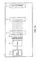
- a common module 3 is applied in a computer system and comprises a first bus 30, at least one first slot 31, a second slot 32, a third slot 33, and a termination circuit card 34.
- the termination circuit card 34 is not fixed in the position represented in Fig. 3a , and the position of the termination circuit card 34 indicates that the termination circuit card 34 is included in the common module 3.
- the first to third slots 31-33 are disposed on the common module 3 and coupled to the first bus 30.
- a main controller 35 of the computer system is installed in the third slot 33.
- the main controller 35 provides a plurality of signals to the first bus 30.
- the main controller 35 is an AMD CPU.
- the common module 3 further comprises a chipset 36 coupled to the main controller 35, and the chipset 36 transmits signals from the main controller 35 to the first bus 30.
- the main controller 35 is an Intel CPU, and the chipset 36 is implemented by a north bridge chipset.
- the signals from the main controller 35 comprise data signals, address signals, and control signals.
- data signals D0-D2 address signals A0-A2, and control signals C0-C2 are given as an example.
- the common module 3 operates in two modes, the first is DDRII SDRAM mode, and the second is DDRIII SDRAM mode.
- Fig. 4a shows the common module 3 in the first mode.
- a DDRII SDRAM 40 is installed in the first slot 31, and the termination circuit card 34 is installed in the second slot 32.
- the termination circuit card 34 comprises a plurality of termination resistors R, and the termination resistors R match the address signals A0-A2 and the control signals C0-C2 in impedance.
- termination resistors RAO-RA2 respectively match the address signals A0-A2
- termination resistors RCO-RC2 respectively match the control signals C0-C2.
- Termination resistors matching the data signals D0-D2 are built into the DDRII SDRAM 40.
- the termination resistors RAO-RA2 and RCO-RC2 are correspondingly coupled to the first bus 30, thus, the termination resistors RAO-RA2 coupled the address signals A0-A2 respectively, and the termination resistors couple the RCO-RC2 control signals C0-C2 respectively.
- Fig. 5 shows the common module 3 in the second mode.
- the DDRII SDRAM 40 is removed from the first slot 31, and the termination circuit card 24 is removed from the second slot 32.
- the DDRIII SDRAM 50 is installed in the second slot 32.
- termination resistors for the data signals D0-D2, the address signals A0-A2, and the control signals C0-C2 are built into the DDRIII SDRAM 50, and the termination circuit card 34 is no longer required.
- the DDRII SDRAM 40 and the termination circuit card 34 are installed when DDRII SDRAM 40 is used, and the DDRIII DRAM 50 is installed when the DDRIII SDRAM50 is used, thus, two main boards with different specifications are not required.
- one first slot 31 is given as an example.
- the common module 3 may comprise a plurality of serially coupled first slots 31 .
- one DDRII SDRAM is installed in one first slot 31.
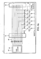
- a common module 6 is applied in a computer system and comprises a first bus 60, at least one first slot 61, a second slot 62, a third slot 63, a plurality of termination resistors R, a plurality of switches SW, and a switch controller 64.
- the first to third slots 61-63 are disposed on the common module 6 and coupled to the first bus 60.
- a main controller 65 of the computer system is installed in the third slot 63.
- the switches SW are coupled between the termination resistors R and the first bus 60.
- the main controller 65 provides a plurality of signals to the first bus 60.
- the main controller 65 is an AMD CPU.
- the common module 6 further comprises a chipset 66 coupled to the main controller 65, and the chipset 66 transmits signals from the main controller 65 to the first bus 60.
- the main controller 65 is an Intel CPU, and the chipset 66 is implemented by a north bridge chipset.
- the signals from the main controller 65 comprise data signals, address signals, and control signals.
- data signals D0-D2, address signals A0-A2, and control signals C0-C2 are given as an example.
- the termination resistors R match the data signals A0-A2 and the control signals C0-C2.
- the termination resistors RAO-RA2 respectively match the address signals A0-A2
- the termination resistors RCO-RC2 respectively match the control signals C0-C2.
- the switches SW comprise switches SWAO-SWA2 and switches SWCO-SWC2.
- the switches SWAO-SWA2 are coupled between the termination resistor RAO-RA2 and the address signals A0-A2 respectively
- the switches SWCO-SWC2 are coupled between the termination resistor RCO-RC2 and the control signals C0-C2 respectively.
- the common module 6 operates in two modes, the first is DDRII SDRAM mode, and the second is DDRIII SDRAM mode.
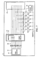
- Fig. 7 shows the common module 6 in the first mode.
- a DDRII SDRAM 70 is installed in the first slot 61, and the switch controller 64 turns on the switches SWAO-SWA2 and SWCO-SWC2.
- the termination resistors RAO-RA2 and RCO-RC2 are correspondingly coupled to the first bus 60, thus, the termination resistors RAO-RA2 couple the address signals A0-A2, and the termination resistors RCO-RC2 coupled control signals C0-C2 respectively.
- termination resistors matching the data signals D0-D2 are built into the DDRII SDRAM 70.
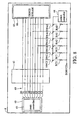
- Fig. 8 shows the common module 6 in the second mode.
- the DDRII SDRAM 70 is removed from the first slot 61, and the DDRIII SDRAM 80 is installed in the second slot 62.
- the switch controller 64 turns off the switches SWAO-SWA2 and SWCO-SWC2.
- termination resistors for the data signals D0-D2, the address signals A0-A2, and the control signals C0-C2 are built into the DDRIII SDRAM 80, and the switches SWAO-SWA2 and SWCO-SWC2 34 are thus no longer coupled to the first bus 60.
- one first slot 61 is given as an example.
- the common module 6 may comprise a plurality of serially coupled first slots 61 .
- one DDRII SDRAM is installed in one first slot 61.
- a common module 9 is applied in a computer system and comprises a first bus 90, at least one first slot 91, a second slot 92, a third slot 93, and a plurality of termination resistors R.
- the first to third slots 91-93 are disposed on the common module 9 and coupled to the first bus 90.
- a main controller 94 of the computer system is installed in the third slot 93.
- the termination resistors R are correspondingly coupled to the first bus 90.
- the main controller 94 provides a plurality of signals to the first bus 90.
- the main controller 94 is an AMD CPU.
- the common module 9 further comprises a chipset 95 coupled to the main controller 94, and the chipset 95 transmits signals from the main controller 94 to the first bus 90.
- the main controller 94 is an Intel CPU, and the chipset 95 is implemented by a north bridge chipset.
- the signals from the main controller 94 comprise data signals, address signals, and control signals.
- data signals D0-D2, address signals A0-A2, and control signals C0-C2 are given as an example.
- the termination resistors R are correspondingly coupled to the first bud 90 and match the data signals A0-A2 and the control signals C0-C2.
- the termination resistors RAO-RA2 respectively match the address signals A0-A2
- the termination resistors RCO-RC2 respectively match the control signals C0-C2.
- the common module 9 operates in two modes, the first is DDRII SDRAM mode, and the second is DDRIII SDRAM mode.
- Fig. 10 shows the common module 9 in the first mode.
- a DDRII SDRAM 100 is installed in the first slot 91.
- Termination resistors matching the data signals D0-D2 are built into the DDRII SDRAM 100.
- the data signals D0-D2 the address signals A0-A2
- the control signals C0-C2 couple the matched termination resistors.
- Fig. 11 shows the common module 9 in the second mode.
- the DDRII SDRAM 100 is removed from the first slot 91, and a DDRIII SDRAM 110 is installed in the second slot 92.
- a value of each termination resistor R is between 0 ohms and 100ohm. In some embodiments, the value of each termination resistor R is between 10 ohms and 100 ohms.
- the common module of the invention eliminates the need for two main boards with different specifications.
- one first slot 91 is given as an example.
- the common module 9 may comprise a plurality of serially coupled first slots 91.
- one DDRII SDRAM is installed in one first slot 91.
Landscapes
- Engineering & Computer Science (AREA)
- Microelectronics & Electronic Packaging (AREA)
- Dram (AREA)
Description
- The invention relates to the method of using a common module, and more particularly to a common module for a double data rate-synchronous II synchronous dynamic random access memory (DDRII SDRAM) and a DDRIII SDRAM.
- Double data rate-synchronous III synchronous dynamic random access memories (DDRIII SDRAMs) have been developed to meet the requirements of high transfer rate and low power consumption. The operating voltage of a DDRIII SDRAM has been reduced over the previous generation from 2.5V to 1.8V, thus, power consumption has been correspondingly reduced, resulting in longer operating life of application devices (such as computers and mobile phones). Additionally, the DDRIII SDRAM packaging techniques, pins, and signals have also improved over previous generations.
-
Fig. 1 shows a conventional main board of a DDRII SDRAM. InFig. 1 , aDDRII SDRAM 11 is installed in a DDRII slot of amain board 1. Amain controller 10 provides data signals DATA, address signals ADD, and control signals CMD to theDDRII SDRAM 11. Themain controller 10 can be an Intel north bridge chipset or an AMD central processing unit (CPU). Referring toFig. 1 , termination resistors RADD and RCMD required for the address signals ADD and the control signals CMD are disposed on themain board 1, and termination resistors RDATA for the data signals DATA are built into theDDRII SDRAM 11. -
Fig. 2 shows a conventional main board of a DDRIII SDRAM. InFig. 2 , aDDRIII SDRAM 21 is installed in a DDRIII slot of a main board 2. Amain controller 20 provides data signals DATA, address signals ADD, and control signals CMD to theDDRIII SDRAM 21. Themain controller 20 can be an Intel north bridge chipset or an AMD CPU. Referring toFig. 2 , termination resistors RDATA, RADD, and RCMD required for the data signals DATA, the address signals ADD, and the control signals CMD are built into theDDRIII SDRAM 21. Compared with themain board 1 of theDDRII SDRAM 11 inFig. 1 , the termination resistors RADD and RCMD of theDDRIII SDRAM 21 are removed from the main board 2 and disposed inside theDDRIII SDRAM 21. - As described, the specifications of a DDRII SDRAM and a DDRIII SDRAM are different. When a DDRII SDRAM or a DDRIII SDRAM is used selectively, a different main board is required for each.
[new]US 6 466 472 B1 discloses a common module for DDR SDRM and SDRAM on a motherboard, which computes and determines the resistance of the terminators on the motherboard so that the work current is controlled within the range allowed by an SDRAM controller, and can achieve the object of a DDR DRAM and SDRAM common layout without the need of an extra quick switch IC. - A common module for a DDRII SDRAM and a DDRIII SDRAM is thus provided. The common module allows selective use of a DDRII SDRAM or a DDRIII SDRAM without requiring two main boards having different specifications.
- A method of using a common module according to the invention is shown in
claim 1. An exemplary embodiment of a common module for a double data rate-synchronous II synchronous dynamic random access memory DDRII SDRAM) and a DDRIII SDRAM, is applied in a computer and comprises a first bus, a termination circuit card, a first slot, and a second slot. The first bus transmits a plurality of signals. The termination circuit card comprises a plurality of termination resistors. The first slot is disposed on the common module and coupled to the first bus. The DDRII SDRAM is selectively installed in the first slot. The second slot is disposed on the common module and coupled to the first bus. The DDRIII SDRAM or the termination circuit card is installed in the second slot. When the DDRII SDRAM is installed in the first slot, the termination circuit card is installed in the second slot. - A detailed description is given in the following embodiments with reference to the accompanying drawings.
- The invention can be more fully understood by reading the subsequent detailed description and examples with references made to the accompanying drawings, wherein:
-
Fig. 1 shows a conventional main board of a DDRII SDRAM; -
Fig. 2 shows a conventional main board of a DDRIII SDRAM; -
Figs. 3a and3b show an exemplary embodiment of a common module for a DDRII SDRAM and a DDRIII SDRAM; -
Fig. 4a shows the common module ofFig. 3a in the first mode; -
Fig. 4b shows the termination circuit card ofFig. 3a ; -
Fig. 5 shows the common module ofFig. 3a in the second mode; -
Figs. 6a and6b show an exemplary embodiment of a common module for a DDRII SDRAM and a DDRIII SDRAM; -
Fig. 7 shows the common module ofFig. 6a in the first mode; -
Fig. 8 shows the common module ofFig. 6a in the second mode; -
Figs. 9a and9b show an exemplary embodiment of a common module for a DDRII SDRAM and a DDRIII SDRAM; -
Fig. 10 shows the common module ofFig. 9a in the first mode; and -
Fig. 11 shows the common module ofFig. 9a in the second mode. - The following description is of the best-contemplated mode of carrying out the invention. This description is made for the purpose of illustrating the general principles of the invention and should not be taken in a limiting sense. The scope of the invention is best determined by reference to the appended claims.
- Common modules for a double data rate-synchronous II synchronous dynamic random access memory (DDRII SDRAM) and a DDRIII SDRAM are provided. In an exemplary embodiment of a common module for a DDRII SDRAM and a DDRIII SDRAM in
Fig. 3a , acommon module 3 is applied in a computer system and comprises afirst bus 30, at least onefirst slot 31, asecond slot 32, athird slot 33, and atermination circuit card 34. Note that thetermination circuit card 34 is not fixed in the position represented inFig. 3a , and the position of thetermination circuit card 34 indicates that thetermination circuit card 34 is included in thecommon module 3. The first to third slots 31-33 are disposed on thecommon module 3 and coupled to thefirst bus 30. Amain controller 35 of the computer system is installed in thethird slot 33. - The
main controller 35 provides a plurality of signals to thefirst bus 30. In some embodiments, themain controller 35 is an AMD CPU. In some embodiments, as shown inFig. 3b , thecommon module 3 further comprises achipset 36 coupled to themain controller 35, and thechipset 36 transmits signals from themain controller 35 to thefirst bus 30. In the embodiment ofFig. 3b , themain controller 35 is an Intel CPU, and thechipset 36 is implemented by a north bridge chipset. - The signals from the
main controller 35 comprise data signals, address signals, and control signals. In the following description, data signals D0-D2, address signals A0-A2, and control signals C0-C2 are given as an example. - The
common module 3 operates in two modes, the first is DDRII SDRAM mode, and the second is DDRIII SDRAM mode. -
Fig. 4a shows thecommon module 3 in the first mode. Referring toFig. 4a , in the first mode, aDDRII SDRAM 40 is installed in thefirst slot 31, and thetermination circuit card 34 is installed in thesecond slot 32. Referring toFig. 4b , thetermination circuit card 34 comprises a plurality of termination resistors R, and the termination resistors R match the address signals A0-A2 and the control signals C0-C2 in impedance. For example, termination resistors RAO-RA2 respectively match the address signals A0-A2, and termination resistors RCO-RC2 respectively match the control signals C0-C2. Termination resistors matching the data signals D0-D2 are built into theDDRII SDRAM 40. When thetermination circuit card 34 is installed in thesecond slot 32, the termination resistors RAO-RA2 and RCO-RC2 are correspondingly coupled to thefirst bus 30, thus, the termination resistors RAO-RA2 coupled the address signals A0-A2 respectively, and the termination resistors couple the RCO-RC2 control signals C0-C2 respectively. -
Fig. 5 shows thecommon module 3 in the second mode. Referring toFig. 5 , in the second mode, theDDRII SDRAM 40 is removed from thefirst slot 31, and the termination circuit card 24 is removed from thesecond slot 32. TheDDRIII SDRAM 50 is installed in thesecond slot 32. According to the specification of theDDRIII SDRAM 50, termination resistors for the data signals D0-D2, the address signals A0-A2, and the control signals C0-C2 are built into theDDRIII SDRAM 50, and thetermination circuit card 34 is no longer required. - According to the embodiment of
Figs. 3a-5 , theDDRII SDRAM 40 and thetermination circuit card 34 are installed whenDDRII SDRAM 40 is used, and theDDRIII DRAM 50 is installed when the DDRIII SDRAM50 is used, thus, two main boards with different specifications are not required. - Additionally, in the embodiment of
Figs. 3a-5 , onefirst slot 31 is given as an example. In practice, thecommon module 3 may comprise a plurality of serially coupledfirst slots 31 . In the first mode, one DDRII SDRAM is installed in onefirst slot 31. - In an exemplary embodiment of a common module for a DDRII SDRAM and a DDRIII SDRAM in
Fig. 6a , acommon module 6 is applied in a computer system and comprises afirst bus 60, at least onefirst slot 61, asecond slot 62, athird slot 63, a plurality of termination resistors R, a plurality of switches SW, and aswitch controller 64. The first to third slots 61-63 are disposed on thecommon module 6 and coupled to thefirst bus 60. Amain controller 65 of the computer system is installed in thethird slot 63. The switches SW are coupled between the termination resistors R and thefirst bus 60. - The
main controller 65 provides a plurality of signals to thefirst bus 60. In some embodiments, themain controller 65 is an AMD CPU. In some embodiments, as shown inFig. 6b , thecommon module 6 further comprises achipset 66 coupled to themain controller 65, and thechipset 66 transmits signals from themain controller 65 to thefirst bus 60. In the embodiment ofFig. 6b , themain controller 65 is an Intel CPU, and thechipset 66 is implemented by a north bridge chipset. - The signals from the
main controller 65 comprise data signals, address signals, and control signals. In the following description, data signals D0-D2, address signals A0-A2, and control signals C0-C2 are given as an example. - The termination resistors R match the data signals A0-A2 and the control signals C0-C2. For example, the termination resistors RAO-RA2 respectively match the address signals A0-A2, and the termination resistors RCO-RC2 respectively match the control signals C0-C2. The switches SW comprise switches SWAO-SWA2 and switches SWCO-SWC2. The switches SWAO-SWA2 are coupled between the termination resistor RAO-RA2 and the address signals A0-A2 respectively, and the switches SWCO-SWC2 are coupled between the termination resistor RCO-RC2 and the control signals C0-C2 respectively.
- The
common module 6 operates in two modes, the first is DDRII SDRAM mode, and the second is DDRIII SDRAM mode. -
Fig. 7 shows thecommon module 6 in the first mode. Referring toFig. 7 , in the first mode, aDDRII SDRAM 70 is installed in thefirst slot 61, and theswitch controller 64 turns on the switches SWAO-SWA2 and SWCO-SWC2. The termination resistors RAO-RA2 and RCO-RC2 are correspondingly coupled to thefirst bus 60, thus, the termination resistors RAO-RA2 couple the address signals A0-A2, and the termination resistors RCO-RC2 coupled control signals C0-C2 respectively. Moreover, termination resistors matching the data signals D0-D2 are built into theDDRII SDRAM 70. -
Fig. 8 shows thecommon module 6 in the second mode. Referring toFig. 8 , in the second mode, theDDRII SDRAM 70 is removed from thefirst slot 61, and theDDRIII SDRAM 80 is installed in thesecond slot 62. Theswitch controller 64 turns off the switches SWAO-SWA2 and SWCO-SWC2. According to the specification of theDDRIII SDRAM 80, termination resistors for the data signals D0-D2, the address signals A0-A2, and the control signals C0-C2 are built into theDDRIII SDRAM 80, and the switches SWAO-SWA2 and SWCO-SWC2 34 are thus no longer coupled to thefirst bus 60. - According to the embodiment of
Figs. 6a-8 , when theDDRII SDRAM 70 or theDDRIII SDRAM 80 is used, the switches SW between the termination resistors R and thefirst bus 61 are selectively turned on or off, thus, two main boards with different specifications are not required. - Moreover, in the embodiment of
Figs. 6a-8 , onefirst slot 61 is given as an example. In practice thecommon module 6 may comprise a plurality of serially coupledfirst slots 61 . In the first mode, one DDRII SDRAM is installed in onefirst slot 61. - In an exemplary embodiment of a common module for a DDRII SDRAM and a DDRIII SDRAM in
Fig. 9a , acommon module 9 is applied in a computer system and comprises afirst bus 90, at least onefirst slot 91, asecond slot 92, athird slot 93, and a plurality of termination resistors R. The first to third slots 91-93 are disposed on thecommon module 9 and coupled to thefirst bus 90. Amain controller 94 of the computer system is installed in thethird slot 93. The termination resistors R are correspondingly coupled to thefirst bus 90. - The
main controller 94 provides a plurality of signals to thefirst bus 90. In some embodiments, themain controller 94 is an AMD CPU. In some embodiments, as shown inFig. 9b , thecommon module 9 further comprises achipset 95 coupled to themain controller 94, and thechipset 95 transmits signals from themain controller 94 to thefirst bus 90. In the embodiment ofFig. 9b , themain controller 94 is an Intel CPU, and thechipset 95 is implemented by a north bridge chipset. - The signals from the
main controller 94 comprise data signals, address signals, and control signals. In the following description, data signals D0-D2, address signals A0-A2, and control signals C0-C2 are given as an example. - The termination resistors R are correspondingly coupled to the
first bud 90 and match the data signals A0-A2 and the control signals C0-C2. For example, the termination resistors RAO-RA2 respectively match the address signals A0-A2, and the termination resistors RCO-RC2 respectively match the control signals C0-C2. - The
common module 9 operates in two modes, the first is DDRII SDRAM mode, and the second is DDRIII SDRAM mode. -
Fig. 10 shows thecommon module 9 in the first mode. Referring toFig. 10 , in the first mode, aDDRII SDRAM 100 is installed in thefirst slot 91. Termination resistors matching the data signals D0-D2 are built into theDDRII SDRAM 100. Thus, the data signals D0-D2, the address signals A0-A2, and the control signals C0-C2 couple the matched termination resistors. -
Fig. 11 shows thecommon module 9 in the second mode. Referring toFig. 11 , in the second mode, theDDRII SDRAM 100 is removed from thefirst slot 91, and aDDRIII SDRAM 110 is installed in thesecond slot 92. - In some embodiments, a value of each termination resistor R is between 0 ohms and 100ohm. In some embodiments, the value of each termination resistor R is between 10 ohms and 100 ohms.
- According to the embodiment of
Figs. 9a-11 , when theDDRII SDRAM 100 or theDDRIII SDRAM 110 is used, theDDRII SDRAM 100 or theDDRIII SDRAM 110 is selectively installed in thecommon module 9. Thus, the common module of the invention eliminates the need for two main boards with different specifications. - Additionally, in the embodiment of
Figs. 9a-11 , onefirst slot 91 is given as an example. In practice, thecommon module 9 may comprise a plurality of serially coupledfirst slots 91. In the first mode, one DDRII SDRAM is installed in onefirst slot 91. - While the invention has been described by way of example and in terms of the preferred embodiments, it is to be understood that the invention is not limited to the disclosed embodiments. To the contrary, it is intended to cover various modifications and similar arrangements (as would be apparent to those skilled in the art). Therefore, the scope of the appended claims should be accorded the broadest interpretation so as to encompass all such modifications and similar arrangements.
Claims (5)
- A method of using a common module (3) operating in a first mode or a second mode and having a first slot (31) and a second slot (32), and a bus (30), wherein a double data rate-synchronous II synchronous dynamic random access memory (DDRII SDRAM) and a DDRIII SDRAM can be inserted, comprising:coupling the first slot (31) and the second slot (32) to the bus (30);characterized by:in the first modeinserting the DDRII SDRAM in the first slot (31); andinserting a termination circuit card (34) in the second slot (32);in the second moderemoving the DDRII SDRAM from the first slot (31);removing the termination circuit card (34) from the second slot (32); andinserting the DDRIIISDRAM in the second slot (32).
- The method as claimed in claim 1 further comprising inserting a main controller (35) in a third slot (33) of the common module (3), wherein the main controller (35) provides signals to the first slot (31) and the second slot (32) through a bus (30).
- The method as claimed in claim 2 further coupling a chipset to the main controller (35) and transmitting the signals to the first bus (30) through the chipset.
- The method as claimed in claim 2,
providing a plurality of first termination resistors (RA0-RA2) and a plurality of second termination resistors (CA0-CA2) to the termination circuit card; and
matching the first termination resistor (RA0-RA2) with address signals (A0-A2) among the signals, and
matching the second termination resistor (CA0-CA2) with control signals (C0-C2) among the signals. - The method as claimed in claim 1, further comprising correspondingly coupling the termination circuit card (34) to the bus (30).
Priority Applications (2)
| Application Number | Priority Date | Filing Date | Title |
|---|---|---|---|
| EP20070112695 EP2026352B1 (en) | 2007-07-18 | 2007-07-18 | Common modules for DDRII SDRAM and DDRIII SDRAM |
| DE200760002635 DE602007002635D1 (en) | 2007-07-18 | 2007-07-18 | Common modules for DDRII SDRAM and DDRIII SDRAM |
Applications Claiming Priority (1)
| Application Number | Priority Date | Filing Date | Title |
|---|---|---|---|
| EP20070112695 EP2026352B1 (en) | 2007-07-18 | 2007-07-18 | Common modules for DDRII SDRAM and DDRIII SDRAM |
Publications (2)
| Publication Number | Publication Date |
|---|---|
| EP2026352A1 EP2026352A1 (en) | 2009-02-18 |
| EP2026352B1 true EP2026352B1 (en) | 2009-09-30 |
Family
ID=39149435
Family Applications (1)
| Application Number | Title | Priority Date | Filing Date |
|---|---|---|---|
| EP20070112695 Not-in-force EP2026352B1 (en) | 2007-07-18 | 2007-07-18 | Common modules for DDRII SDRAM and DDRIII SDRAM |
Country Status (2)
| Country | Link |
|---|---|
| EP (1) | EP2026352B1 (en) |
| DE (1) | DE602007002635D1 (en) |
Family Cites Families (3)
| Publication number | Priority date | Publication date | Assignee | Title |
|---|---|---|---|---|
| US6466472B1 (en) | 2001-04-13 | 2002-10-15 | Giga-Byte Technology Co., Ltd. | Common module for DDR SDRAM and SDRAM |
| US8391039B2 (en) * | 2001-04-24 | 2013-03-05 | Rambus Inc. | Memory module with termination component |
| JP4419049B2 (en) * | 2003-04-21 | 2010-02-24 | エルピーダメモリ株式会社 | Memory module and memory system |
-
2007
- 2007-07-18 EP EP20070112695 patent/EP2026352B1/en not_active Not-in-force
- 2007-07-18 DE DE200760002635 patent/DE602007002635D1/en active Active
Also Published As
| Publication number | Publication date |
|---|---|
| EP2026352A1 (en) | 2009-02-18 |
| DE602007002635D1 (en) | 2009-11-12 |
Similar Documents
| Publication | Publication Date | Title |
|---|---|---|
| US11994982B2 (en) | Memory module with distributed data buffers | |
| CN100592276C (en) | Commands control different operations in different chips | |
| US6061263A (en) | Small outline rambus in-line memory module | |
| US8130560B1 (en) | Multi-rank partial width memory modules | |
| US7342411B2 (en) | Dynamic on-die termination launch latency reduction | |
| US20050182858A1 (en) | Portable memory device with multiple I/O interfaces | |
| JP2003085122A (en) | Computer system and switch connector | |
| US6535411B2 (en) | Memory module and computer system comprising a memory module | |
| US9275699B2 (en) | Memory with alternative command interfaces | |
| GB2446696A (en) | Dynamic on-die termination for memory devices using different byte lane lengths | |
| KR100375147B1 (en) | Circuit module | |
| US8279689B2 (en) | Low power termination for memory modules | |
| US7562193B2 (en) | Memory with single and dual mode access | |
| US20100070694A1 (en) | Computer system having ram slots with different specifications | |
| JP4823009B2 (en) | Memory card and host device | |
| US6362996B2 (en) | Terminating circuit module used in a computer system | |
| US7825681B2 (en) | Common modules for DDRII SDRAM and DDRIII SDRAM | |
| US20080065789A1 (en) | Multi-purpose IO system | |
| US6466472B1 (en) | Common module for DDR SDRAM and SDRAM | |
| CN101295846A (en) | Adapter plate and mainboard | |
| US7539035B2 (en) | Memory system capable of changing configuration of memory modules | |
| EP2026352A1 (en) | Common modules for DDRII SDRAM and DDRIII SDRAM | |
| KR100891951B1 (en) | Common module for ddr? sdram and ddr? sdram | |
| CN101315616A (en) | DDRII SDRAM and DDRIII SDRAM common module | |
| US20080101046A1 (en) | Motherboard |
Legal Events
| Date | Code | Title | Description |
|---|---|---|---|
| PUAI | Public reference made under article 153(3) epc to a published international application that has entered the european phase |
Free format text: ORIGINAL CODE: 0009012 |
|
| 17P | Request for examination filed |
Effective date: 20080912 |
|
| AK | Designated contracting states |
Kind code of ref document: A1 Designated state(s): AT BE BG CH CY CZ DE DK EE ES FI FR GB GR HU IE IS IT LI LT LU LV MC MT NL PL PT RO SE SI SK TR |
|
| AX | Request for extension of the european patent |
Extension state: AL BA HR MK RS |
|
| GRAP | Despatch of communication of intention to grant a patent |
Free format text: ORIGINAL CODE: EPIDOSNIGR1 |
|
| GRAS | Grant fee paid |
Free format text: ORIGINAL CODE: EPIDOSNIGR3 |
|
| GRAA | (expected) grant |
Free format text: ORIGINAL CODE: 0009210 |
|
| AK | Designated contracting states |
Kind code of ref document: B1 Designated state(s): DE FR GB |
|
| REG | Reference to a national code |
Ref country code: GB Ref legal event code: FG4D |
|
| AKX | Designation fees paid |
Designated state(s): DE FR GB |
|
| REF | Corresponds to: |
Ref document number: 602007002635 Country of ref document: DE Date of ref document: 20091112 Kind code of ref document: P |
|
| PLBE | No opposition filed within time limit |
Free format text: ORIGINAL CODE: 0009261 |
|
| STAA | Information on the status of an ep patent application or granted ep patent |
Free format text: STATUS: NO OPPOSITION FILED WITHIN TIME LIMIT |
|
| 26N | No opposition filed |
Effective date: 20100701 |
|
| PGFP | Annual fee paid to national office [announced via postgrant information from national office to epo] |
Ref country code: GB Payment date: 20130610 Year of fee payment: 7 |
|
| PGFP | Annual fee paid to national office [announced via postgrant information from national office to epo] |
Ref country code: FR Payment date: 20130628 Year of fee payment: 7 |
|
| PGFP | Annual fee paid to national office [announced via postgrant information from national office to epo] |
Ref country code: DE Payment date: 20130610 Year of fee payment: 7 |
|
| REG | Reference to a national code |
Ref country code: DE Ref legal event code: R119 Ref document number: 602007002635 Country of ref document: DE |
|
| GBPC | Gb: european patent ceased through non-payment of renewal fee |
Effective date: 20140718 |
|
| REG | Reference to a national code |
Ref country code: FR Ref legal event code: ST Effective date: 20150331 |
|
| PG25 | Lapsed in a contracting state [announced via postgrant information from national office to epo] |
Ref country code: DE Free format text: LAPSE BECAUSE OF NON-PAYMENT OF DUE FEES Effective date: 20150203 |
|
| REG | Reference to a national code |
Ref country code: DE Ref legal event code: R119 Ref document number: 602007002635 Country of ref document: DE Effective date: 20150203 |
|
| PG25 | Lapsed in a contracting state [announced via postgrant information from national office to epo] |
Ref country code: GB Free format text: LAPSE BECAUSE OF NON-PAYMENT OF DUE FEES Effective date: 20140718 Ref country code: FR Free format text: LAPSE BECAUSE OF NON-PAYMENT OF DUE FEES Effective date: 20140731 |