EP2024784B1 - Multistable reflective liquid crystal device - Google Patents
Multistable reflective liquid crystal device Download PDFInfo
- Publication number
- EP2024784B1 EP2024784B1 EP07733096A EP07733096A EP2024784B1 EP 2024784 B1 EP2024784 B1 EP 2024784B1 EP 07733096 A EP07733096 A EP 07733096A EP 07733096 A EP07733096 A EP 07733096A EP 2024784 B1 EP2024784 B1 EP 2024784B1
- Authority
- EP
- European Patent Office
- Prior art keywords
- liquid crystal
- multistable
- crystal device
- cavities
- cavity
- Prior art date
- Legal status (The legal status is an assumption and is not a legal conclusion. Google has not performed a legal analysis and makes no representation as to the accuracy of the status listed.)
- Not-in-force
Links
Images


Classifications
-
- G—PHYSICS
- G02—OPTICS
- G02F—OPTICAL DEVICES OR ARRANGEMENTS FOR THE CONTROL OF LIGHT BY MODIFICATION OF THE OPTICAL PROPERTIES OF THE MEDIA OF THE ELEMENTS INVOLVED THEREIN; NON-LINEAR OPTICS; FREQUENCY-CHANGING OF LIGHT; OPTICAL LOGIC ELEMENTS; OPTICAL ANALOGUE/DIGITAL CONVERTERS
- G02F1/00—Devices or arrangements for the control of the intensity, colour, phase, polarisation or direction of light arriving from an independent light source, e.g. switching, gating or modulating; Non-linear optics
- G02F1/01—Devices or arrangements for the control of the intensity, colour, phase, polarisation or direction of light arriving from an independent light source, e.g. switching, gating or modulating; Non-linear optics for the control of the intensity, phase, polarisation or colour
- G02F1/13—Devices or arrangements for the control of the intensity, colour, phase, polarisation or direction of light arriving from an independent light source, e.g. switching, gating or modulating; Non-linear optics for the control of the intensity, phase, polarisation or colour based on liquid crystals, e.g. single liquid crystal display cells
- G02F1/133—Constructional arrangements; Operation of liquid crystal cells; Circuit arrangements
- G02F1/1333—Constructional arrangements; Manufacturing methods
-
- G—PHYSICS
- G02—OPTICS
- G02F—OPTICAL DEVICES OR ARRANGEMENTS FOR THE CONTROL OF LIGHT BY MODIFICATION OF THE OPTICAL PROPERTIES OF THE MEDIA OF THE ELEMENTS INVOLVED THEREIN; NON-LINEAR OPTICS; FREQUENCY-CHANGING OF LIGHT; OPTICAL LOGIC ELEMENTS; OPTICAL ANALOGUE/DIGITAL CONVERTERS
- G02F1/00—Devices or arrangements for the control of the intensity, colour, phase, polarisation or direction of light arriving from an independent light source, e.g. switching, gating or modulating; Non-linear optics
- G02F1/01—Devices or arrangements for the control of the intensity, colour, phase, polarisation or direction of light arriving from an independent light source, e.g. switching, gating or modulating; Non-linear optics for the control of the intensity, phase, polarisation or colour
- G02F1/13—Devices or arrangements for the control of the intensity, colour, phase, polarisation or direction of light arriving from an independent light source, e.g. switching, gating or modulating; Non-linear optics for the control of the intensity, phase, polarisation or colour based on liquid crystals, e.g. single liquid crystal display cells
- G02F1/133—Constructional arrangements; Operation of liquid crystal cells; Circuit arrangements
- G02F1/1333—Constructional arrangements; Manufacturing methods
- G02F1/1337—Surface-induced orientation of the liquid crystal molecules, e.g. by alignment layers
-
- G—PHYSICS
- G02—OPTICS
- G02F—OPTICAL DEVICES OR ARRANGEMENTS FOR THE CONTROL OF LIGHT BY MODIFICATION OF THE OPTICAL PROPERTIES OF THE MEDIA OF THE ELEMENTS INVOLVED THEREIN; NON-LINEAR OPTICS; FREQUENCY-CHANGING OF LIGHT; OPTICAL LOGIC ELEMENTS; OPTICAL ANALOGUE/DIGITAL CONVERTERS
- G02F1/00—Devices or arrangements for the control of the intensity, colour, phase, polarisation or direction of light arriving from an independent light source, e.g. switching, gating or modulating; Non-linear optics
- G02F1/01—Devices or arrangements for the control of the intensity, colour, phase, polarisation or direction of light arriving from an independent light source, e.g. switching, gating or modulating; Non-linear optics for the control of the intensity, phase, polarisation or colour
- G02F1/13—Devices or arrangements for the control of the intensity, colour, phase, polarisation or direction of light arriving from an independent light source, e.g. switching, gating or modulating; Non-linear optics for the control of the intensity, phase, polarisation or colour based on liquid crystals, e.g. single liquid crystal display cells
- G02F1/133—Constructional arrangements; Operation of liquid crystal cells; Circuit arrangements
- G02F1/1333—Constructional arrangements; Manufacturing methods
- G02F1/133377—Cells with plural compartments or having plurality of liquid crystal microcells partitioned by walls, e.g. one microcell per pixel
-
- G—PHYSICS
- G02—OPTICS
- G02F—OPTICAL DEVICES OR ARRANGEMENTS FOR THE CONTROL OF LIGHT BY MODIFICATION OF THE OPTICAL PROPERTIES OF THE MEDIA OF THE ELEMENTS INVOLVED THEREIN; NON-LINEAR OPTICS; FREQUENCY-CHANGING OF LIGHT; OPTICAL LOGIC ELEMENTS; OPTICAL ANALOGUE/DIGITAL CONVERTERS
- G02F1/00—Devices or arrangements for the control of the intensity, colour, phase, polarisation or direction of light arriving from an independent light source, e.g. switching, gating or modulating; Non-linear optics
- G02F1/01—Devices or arrangements for the control of the intensity, colour, phase, polarisation or direction of light arriving from an independent light source, e.g. switching, gating or modulating; Non-linear optics for the control of the intensity, phase, polarisation or colour
- G02F1/13—Devices or arrangements for the control of the intensity, colour, phase, polarisation or direction of light arriving from an independent light source, e.g. switching, gating or modulating; Non-linear optics for the control of the intensity, phase, polarisation or colour based on liquid crystals, e.g. single liquid crystal display cells
- G02F1/133—Constructional arrangements; Operation of liquid crystal cells; Circuit arrangements
- G02F1/1333—Constructional arrangements; Manufacturing methods
- G02F1/1335—Structural association of cells with optical devices, e.g. polarisers or reflectors
-
- G—PHYSICS
- G02—OPTICS
- G02F—OPTICAL DEVICES OR ARRANGEMENTS FOR THE CONTROL OF LIGHT BY MODIFICATION OF THE OPTICAL PROPERTIES OF THE MEDIA OF THE ELEMENTS INVOLVED THEREIN; NON-LINEAR OPTICS; FREQUENCY-CHANGING OF LIGHT; OPTICAL LOGIC ELEMENTS; OPTICAL ANALOGUE/DIGITAL CONVERTERS
- G02F1/00—Devices or arrangements for the control of the intensity, colour, phase, polarisation or direction of light arriving from an independent light source, e.g. switching, gating or modulating; Non-linear optics
- G02F1/01—Devices or arrangements for the control of the intensity, colour, phase, polarisation or direction of light arriving from an independent light source, e.g. switching, gating or modulating; Non-linear optics for the control of the intensity, phase, polarisation or colour
- G02F1/13—Devices or arrangements for the control of the intensity, colour, phase, polarisation or direction of light arriving from an independent light source, e.g. switching, gating or modulating; Non-linear optics for the control of the intensity, phase, polarisation or colour based on liquid crystals, e.g. single liquid crystal display cells
- G02F1/133—Constructional arrangements; Operation of liquid crystal cells; Circuit arrangements
- G02F1/1333—Constructional arrangements; Manufacturing methods
- G02F1/1335—Structural association of cells with optical devices, e.g. polarisers or reflectors
- G02F1/133553—Reflecting elements
-
- G—PHYSICS
- G02—OPTICS
- G02F—OPTICAL DEVICES OR ARRANGEMENTS FOR THE CONTROL OF LIGHT BY MODIFICATION OF THE OPTICAL PROPERTIES OF THE MEDIA OF THE ELEMENTS INVOLVED THEREIN; NON-LINEAR OPTICS; FREQUENCY-CHANGING OF LIGHT; OPTICAL LOGIC ELEMENTS; OPTICAL ANALOGUE/DIGITAL CONVERTERS
- G02F1/00—Devices or arrangements for the control of the intensity, colour, phase, polarisation or direction of light arriving from an independent light source, e.g. switching, gating or modulating; Non-linear optics
- G02F1/01—Devices or arrangements for the control of the intensity, colour, phase, polarisation or direction of light arriving from an independent light source, e.g. switching, gating or modulating; Non-linear optics for the control of the intensity, phase, polarisation or colour
- G02F1/13—Devices or arrangements for the control of the intensity, colour, phase, polarisation or direction of light arriving from an independent light source, e.g. switching, gating or modulating; Non-linear optics for the control of the intensity, phase, polarisation or colour based on liquid crystals, e.g. single liquid crystal display cells
- G02F1/133—Constructional arrangements; Operation of liquid crystal cells; Circuit arrangements
- G02F1/1333—Constructional arrangements; Manufacturing methods
- G02F1/1337—Surface-induced orientation of the liquid crystal molecules, e.g. by alignment layers
- G02F1/133707—Structures for producing distorted electric fields, e.g. bumps, protrusions, recesses, slits in pixel electrodes
-
- G—PHYSICS
- G02—OPTICS
- G02F—OPTICAL DEVICES OR ARRANGEMENTS FOR THE CONTROL OF LIGHT BY MODIFICATION OF THE OPTICAL PROPERTIES OF THE MEDIA OF THE ELEMENTS INVOLVED THEREIN; NON-LINEAR OPTICS; FREQUENCY-CHANGING OF LIGHT; OPTICAL LOGIC ELEMENTS; OPTICAL ANALOGUE/DIGITAL CONVERTERS
- G02F1/00—Devices or arrangements for the control of the intensity, colour, phase, polarisation or direction of light arriving from an independent light source, e.g. switching, gating or modulating; Non-linear optics
- G02F1/01—Devices or arrangements for the control of the intensity, colour, phase, polarisation or direction of light arriving from an independent light source, e.g. switching, gating or modulating; Non-linear optics for the control of the intensity, phase, polarisation or colour
- G02F1/13—Devices or arrangements for the control of the intensity, colour, phase, polarisation or direction of light arriving from an independent light source, e.g. switching, gating or modulating; Non-linear optics for the control of the intensity, phase, polarisation or colour based on liquid crystals, e.g. single liquid crystal display cells
- G02F1/133—Constructional arrangements; Operation of liquid crystal cells; Circuit arrangements
- G02F1/1333—Constructional arrangements; Manufacturing methods
- G02F1/1337—Surface-induced orientation of the liquid crystal molecules, e.g. by alignment layers
- G02F1/133753—Surface-induced orientation of the liquid crystal molecules, e.g. by alignment layers with different alignment orientations or pretilt angles on a same surface, e.g. for grey scale or improved viewing angle
-
- G—PHYSICS
- G02—OPTICS
- G02F—OPTICAL DEVICES OR ARRANGEMENTS FOR THE CONTROL OF LIGHT BY MODIFICATION OF THE OPTICAL PROPERTIES OF THE MEDIA OF THE ELEMENTS INVOLVED THEREIN; NON-LINEAR OPTICS; FREQUENCY-CHANGING OF LIGHT; OPTICAL LOGIC ELEMENTS; OPTICAL ANALOGUE/DIGITAL CONVERTERS
- G02F1/00—Devices or arrangements for the control of the intensity, colour, phase, polarisation or direction of light arriving from an independent light source, e.g. switching, gating or modulating; Non-linear optics
- G02F1/01—Devices or arrangements for the control of the intensity, colour, phase, polarisation or direction of light arriving from an independent light source, e.g. switching, gating or modulating; Non-linear optics for the control of the intensity, phase, polarisation or colour
- G02F1/13—Devices or arrangements for the control of the intensity, colour, phase, polarisation or direction of light arriving from an independent light source, e.g. switching, gating or modulating; Non-linear optics for the control of the intensity, phase, polarisation or colour based on liquid crystals, e.g. single liquid crystal display cells
- G02F1/133—Constructional arrangements; Operation of liquid crystal cells; Circuit arrangements
- G02F1/1333—Constructional arrangements; Manufacturing methods
- G02F1/1343—Electrodes
-
- G—PHYSICS
- G02—OPTICS
- G02F—OPTICAL DEVICES OR ARRANGEMENTS FOR THE CONTROL OF LIGHT BY MODIFICATION OF THE OPTICAL PROPERTIES OF THE MEDIA OF THE ELEMENTS INVOLVED THEREIN; NON-LINEAR OPTICS; FREQUENCY-CHANGING OF LIGHT; OPTICAL LOGIC ELEMENTS; OPTICAL ANALOGUE/DIGITAL CONVERTERS
- G02F1/00—Devices or arrangements for the control of the intensity, colour, phase, polarisation or direction of light arriving from an independent light source, e.g. switching, gating or modulating; Non-linear optics
- G02F1/01—Devices or arrangements for the control of the intensity, colour, phase, polarisation or direction of light arriving from an independent light source, e.g. switching, gating or modulating; Non-linear optics for the control of the intensity, phase, polarisation or colour
- G02F1/13—Devices or arrangements for the control of the intensity, colour, phase, polarisation or direction of light arriving from an independent light source, e.g. switching, gating or modulating; Non-linear optics for the control of the intensity, phase, polarisation or colour based on liquid crystals, e.g. single liquid crystal display cells
- G02F1/133—Constructional arrangements; Operation of liquid crystal cells; Circuit arrangements
- G02F1/1333—Constructional arrangements; Manufacturing methods
- G02F1/1343—Electrodes
- G02F1/134309—Electrodes characterised by their geometrical arrangement
- G02F1/134363—Electrodes characterised by their geometrical arrangement for applying an electric field parallel to the substrate, i.e. in-plane switching [IPS]
-
- G—PHYSICS
- G02—OPTICS
- G02F—OPTICAL DEVICES OR ARRANGEMENTS FOR THE CONTROL OF LIGHT BY MODIFICATION OF THE OPTICAL PROPERTIES OF THE MEDIA OF THE ELEMENTS INVOLVED THEREIN; NON-LINEAR OPTICS; FREQUENCY-CHANGING OF LIGHT; OPTICAL LOGIC ELEMENTS; OPTICAL ANALOGUE/DIGITAL CONVERTERS
- G02F1/00—Devices or arrangements for the control of the intensity, colour, phase, polarisation or direction of light arriving from an independent light source, e.g. switching, gating or modulating; Non-linear optics
- G02F1/01—Devices or arrangements for the control of the intensity, colour, phase, polarisation or direction of light arriving from an independent light source, e.g. switching, gating or modulating; Non-linear optics for the control of the intensity, phase, polarisation or colour
- G02F1/13—Devices or arrangements for the control of the intensity, colour, phase, polarisation or direction of light arriving from an independent light source, e.g. switching, gating or modulating; Non-linear optics for the control of the intensity, phase, polarisation or colour based on liquid crystals, e.g. single liquid crystal display cells
- G02F1/137—Devices or arrangements for the control of the intensity, colour, phase, polarisation or direction of light arriving from an independent light source, e.g. switching, gating or modulating; Non-linear optics for the control of the intensity, phase, polarisation or colour based on liquid crystals, e.g. single liquid crystal display cells characterised by the electro-optical or magneto-optical effect, e.g. field-induced phase transition, orientation effect, guest-host interaction or dynamic scattering
- G02F1/139—Devices or arrangements for the control of the intensity, colour, phase, polarisation or direction of light arriving from an independent light source, e.g. switching, gating or modulating; Non-linear optics for the control of the intensity, phase, polarisation or colour based on liquid crystals, e.g. single liquid crystal display cells characterised by the electro-optical or magneto-optical effect, e.g. field-induced phase transition, orientation effect, guest-host interaction or dynamic scattering based on orientation effects in which the liquid crystal remains transparent
-
- G—PHYSICS
- G02—OPTICS
- G02F—OPTICAL DEVICES OR ARRANGEMENTS FOR THE CONTROL OF LIGHT BY MODIFICATION OF THE OPTICAL PROPERTIES OF THE MEDIA OF THE ELEMENTS INVOLVED THEREIN; NON-LINEAR OPTICS; FREQUENCY-CHANGING OF LIGHT; OPTICAL LOGIC ELEMENTS; OPTICAL ANALOGUE/DIGITAL CONVERTERS
- G02F1/00—Devices or arrangements for the control of the intensity, colour, phase, polarisation or direction of light arriving from an independent light source, e.g. switching, gating or modulating; Non-linear optics
- G02F1/01—Devices or arrangements for the control of the intensity, colour, phase, polarisation or direction of light arriving from an independent light source, e.g. switching, gating or modulating; Non-linear optics for the control of the intensity, phase, polarisation or colour
- G02F1/13—Devices or arrangements for the control of the intensity, colour, phase, polarisation or direction of light arriving from an independent light source, e.g. switching, gating or modulating; Non-linear optics for the control of the intensity, phase, polarisation or colour based on liquid crystals, e.g. single liquid crystal display cells
- G02F1/137—Devices or arrangements for the control of the intensity, colour, phase, polarisation or direction of light arriving from an independent light source, e.g. switching, gating or modulating; Non-linear optics for the control of the intensity, phase, polarisation or colour based on liquid crystals, e.g. single liquid crystal display cells characterised by the electro-optical or magneto-optical effect, e.g. field-induced phase transition, orientation effect, guest-host interaction or dynamic scattering
- G02F1/139—Devices or arrangements for the control of the intensity, colour, phase, polarisation or direction of light arriving from an independent light source, e.g. switching, gating or modulating; Non-linear optics for the control of the intensity, phase, polarisation or colour based on liquid crystals, e.g. single liquid crystal display cells characterised by the electro-optical or magneto-optical effect, e.g. field-induced phase transition, orientation effect, guest-host interaction or dynamic scattering based on orientation effects in which the liquid crystal remains transparent
- G02F1/1391—Bistable or multi-stable liquid crystal cells
Definitions
- the present invention relates to a multistable reflective liquid crystal device and a liquid crystal display that includes such a device.
- Liquid crystal materials consist of rod-like molecules that prefer to align parallel to each other and are capable of being aligned by applied electric fields.
- the long-range order caused by the local alignment of molecules enables the "director", the average molecular direction, to be defined.
- the long and short axes of these molecules exhibit different optical properties and certain molecular orientations can therefore alter the polarisation and intensity of incident light.
- These reorientation and polarisation effects can be utilised in conjunction with optical elements such as polarising and reflective layers to produce optical devices such as optical switches, changeable phase gratings or displays.
- LC devices commonly have two transparent substrates, with semi-transparent electrodes that may be patterned into pixels on the inner side of each substrate, sandwiching a liquid crystal (LC) material between them.
- a reflective coating may be placed at one substrate if the device is to be used to reflect incident light once it has passed through the liquid crystal layer rather than in a transmissive mode.
- Optical polarisers are usually placed on the outer surface of one or both substrates. Between the liquid crystal layer and each electrode/substrate an alignment layer is used to specify the orientation of the LC molecules close to the substrate.
- Each pixel may be addressed "passively” using a voltage applied across the pixel row and column electrodes or “actively” using thin film transistors to selectively apply an electric field across a single pixel. This electric field may be used to switch the liquid crystal molecules between two orientational states, each with a different effect on the light passing through the LC layer such that, depending on the state, the light may either be transmitted through or blocked by the polariser(s).
- twisted nematic configurations In these devices, alignment layers are used to orient the LC molecules close to opposing substrates in perpendicular directions to each other. In the state where no electric field is applied across a pixel, the perpendicular LC alignment close to the substrates results in a 90° twist in LC orientation as one moves from surface to surface. This has the effect of rotating the polarisation of the light through 90°.
- polarisers When polarisers are placed parallel to the alignment directions at each substrate, incident light becomes initially polarised by the first polariser in one direction, then the polarisation direction of the light is rotated 90° by the LC to coincide with the second polariser at the other , substrate, such that light is output from the pixel.
- Coloured filters may be placed over the pixel to produce coloured pixels.
- the LC aligns with the direction of the field, i.e. perpendicular to the plane of both substrates.
- the LC molecules are aligned parallel to the direction of the propagation of the light, no change in polarisation of the light due to the LC configuration takes place.
- polarised light from the first polariser is blocked by the second polariser in the perpendicular direction.
- This type of device is "transmissive" since the incident light passes through the device from a light source (i.e. a backlight in a display module) on one side to the observer on the other.
- An alternative method of displaying information using a liquid crystal device is through the use of a "reflective" LC device.
- a typical reflective device is constructed in a similar way to a transmissive device except the polariser furthest away from the observer is replaced by a reflective element.
- Light is incident from the same side of the device as the observer and is initially polarised by the polariser in one direction.
- One of the possible LC configurations is such that the polarisation direction of the light is rotated by 45° by the LC, before it is reflected by the reflective element and then rotated again by 45° by the LC.
- the total rotation of the polarisation of light by 90° means that the light is blocked by the polariser.
- a reorientation of the LC occurs such that the LC configuration does not affect the polarisation of light and the incident light is polarised, transmitted through the LC, reflected and transmitted through the LC again with no change in polarisation direction, so that the polariser allows the light to be emitted and observed.
- Coloured filters may be placed over the pixel to produce coloured pixels.
- LC displays have many advantages such as being very flat, light and robust when compared with other display types such as cathode ray tubes. As such they are ideal for small portable devices such as mobile phones and PDAs. However, they have a high-energy demand due to the need for constant power to be applied to hold a pixel in one state. Furthermore, transmissive displays typically require backlighting from a light source to achieve a bright picture with high contrast, which in turn further increases the power consumption, leading to a shortened battery life. In addition, since these systems employ out of plane switching, where the LC molecules align themselves perpendicularly to the plane of the substrates in the presence of the electric field, birefringence effects can lead to a loss of contrast when viewed from the side. The resultant geometry may also lead to colour distortion due to parallax effects.
- multistable or, specifically, reflective bistable liquid crystal technology the LC has more than one stable director configuration. As such, once switched into a stable state, the LC remains in that state until an electric field is applied to change the configuration. This type of operation requires less power since power is only supplied to change states and not supplied continuously to maintain a state.
- the reflective aspect of such a technology removes the need for a backlight, further reducing the power consumption.
- LC devices having a number of possible multistable systems are described.
- zenithal multistable devices are described which produce distortion out of the substrate plane.
- In-plane multistable devices are also described that rely on patterned alignment regions on the substrates.
- WO 97/14990 describes a further example of a bistable device.
- This has a surface alignment monograting on at least one of the substrates.
- the surface monograting has a groove height to width ratio that leads to approximately equal energy for two director alignment arrangements.
- the director alignment arrangements differ from each other primarily by angle of the director from the plane of the substrate.
- the device is switched using appropriate voltage pulses.
- bistable liquid crystal devices involve having an array of either posts or holes placed on one of the substrates. Devices of this type are described in EP 1,271,225 and EP 1,139,151 . The presence of posts or holes allows multiple director orientations to be stable. The difference between the director orientations is primarily in the difference in director angle from the main plane of the substrates. Switching between these states is achieved using appropriate voltage pulses coupling to the molecular dipoles.
- each stable state has a different effect on the polarisation of light and this can be used in conjunction with suitably oriented polarisers to allow or block the transmittance of light.
- These systems may be used with light transmitted through the device or reflected from a surface at the back of the device. Variations in surface treatments on the sub-pixel level may be used to achieve greyscale. Whilst these provide some advantages over more conventional arrangements, they suffer from the fact that the switching is out of plane, which can lead to loss of contrast at oblique viewing angles and colour deformations due to parallax errors.
- Some of the devices described above may contain LC defect regions.
- the molecular direction is influenced by the container surfaces. This can lead to conflicts at certain regions, resulting in defects.
- the molecules align themselves in such a fashion so that a high distortion energy structure, associated with a reduction in molecular order, is formed, as discussed by Repnik et al. in European Journal of Physics, Vol. 24, pages 481-492 (2003 ).
- a high distortion energy structure associated with a reduction in molecular order
- WO 2006/059128 describes a bistable device with corner distortion regions for switching by application of an electric field and a 90° re-alignment between two stable states.
- a reflective multistable liquid crystal device as claimed in claim 1 below.
- the present invention takes advantage of these and uses them to provide multistable states. Indeed, the walls of the containment structures are used to induce the formation of defect structures. By applying an appropriate electric field, the distortion region(s) can be switched between these states. This can be done substantially in-plane, thereby avoiding or at least reducing the loss of contrast at oblique viewing.
- the confined containment structure of the present invention affords advantages over unconfined systems, such as those described in Thurston et al. IEEE Transactions on Electronic Devices Ed-27, no. 11, pp. 2069-2080 1980 , in that the open region between the switchable regions of the Thurston device will detrimentally affect the contrast and reflectance characteristics in the unconfined devices whereas in the present invention the containment structure is homogeneous and has a calculable fixed optical effect which may be minimised.
- the device and method of the invention may be used for various applications including a display substrate, a phase device for telecommunications, an optical switch or a changeable phase grating.
- Containing liquid crystals within containment structures having certain shapes and dimensions can lead to the tendency of the liquid crystal molecules to arrange themselves into one of a multiple of stable states, each stable state having differing director structures and possibly different locations of regions of high distortion.
- a high distortion location is a region where the liquid crystal molecular order is significantly reduced compared to the bulk and a large elastic distortion occurs, as discussed by Repnik et al. in European Journal of Physics, Vol. 24, pages 481-492 (2003 ).
- Figures 1(a) and (b) shows a reflective liquid crystal device having a liquid crystal material 10 contained within a containment structure 20 that defines a plurality of openings 21.
- the containment structure 20 is sandwiched between two transparent substrates 30, 35, which may have alignment layer preparations 40, 45 adhered to faces in contact with the liquid crystal material 10.
- the containment structure 20 and the substrates 30, 35 together define a plurality of cavities for containing the liquid crystal material 10.
- the liquid crystal material 10 within each cavity completely fills it, so that the liquid crystal material is in direct contact with all of the cavity walls/surfaces, and adjacent cavities are completely isolated from each other.
- a polariser 50 is laminated to the outside of one transparent substrate 30 and a colour filter 70 may be located over it.
- the colour filter 70 may be provided as a series of strips or squares of transparent coloured sections. Each cavity may have an area of colour filter 70 associated with it. Each colour filter may cover several cavities.
- the colour filter 70 may have red, green and blue transparent coloured sections.
- Laminated to the substrate 35 at the rear of the device is a reflective layer 85 that acts as a reflective back plate.
- the cavities of the containment structure 20 have an approximately hexagonal cross section having sharp or rounded corners 120, 130, 140, 150, 160, 170 in a plane parallel to the transparent substrates 30, 35.
- the cross section of the cavities may be any polygon with corners such that the alignment of the bulk liquid crystal is at an oblique angle to the alignment of liquid crystal in another stable state.
- the length of the sides of the hexagonal cross section of the cavity may be different and may be between 10 and 100 ⁇ m long and the cavity should be between 1 and 50 ⁇ m deep.
- the hexagonal cross section allows the possibility of two or more stable states.
- the transparent substrates 30, 35 On their surfaces and facing the liquid crystal 10, the transparent substrates 30, 35 have patterned transparent electrodes 75, 80 formed for example from a thin layer of conducting material such as Indium Tin Oxide. To achieve in-plane switching, these electrodes 75, 80 may be used to produce an electric field with a component in a plane parallel to that of the transparent substrates 30, 35. This may be achieved for example by having electrodes staggered so that the counter electrode is not directly below the working electrode. Alternatively or additionally, electrodes may be incorporated into the cavity walls in order to produce an electric field parallel to the substrate. Each electrode may be associated with one or more cavities and there may be more than one set of electrodes to enable switching between the two or more stable states.
- a thin layer of conducting material such as Indium Tin Oxide.
- the cavities in the containment structure 20 and associated electrodes 75, 80 may correspond to a pixel of a displayed image or several cavities and electrodes 75, 80 may correspond to one pixel in order to achieve a greyscale or full colour output.
- the alignment of the liquid crystal molecules 10 on the containment structure 20 walls is dictated by a number of factors.
- the containment structure 20 is made of a polymeric material the polymer direction dictates the molecule direction.
- a photoresist material such as SU8 is used to create the containment structure 20 the molecules prefer to lie in any direction parallel to the surface.
- a homeotropic alignment surface treatment is used the molecules prefer to lie perpendicular to the cavity surfaces with the molecules preferring parallel alignment at the transparent substrates 30, 35.
- the liquid crystal molecules 10 in the bulk of the region tend to align themselves at 45° to the sidewalls of the cavities and in a plane parallel to the transparent substrates 30, 35.
- high distortion regions 100, 110 form at two opposing corners of the cavity 120, 150.
- the relatively sharp transition between adjoining walls of the cavity is advantageous in promoting the formation of localised high distortion regions and pinning these regions to the corners 120, 150 of the cavity.
- the liquid crystal molecules 10 in the region of these high distortion sites 100, 110 are oriented differently to the majority of liquid crystal molecules 10 in the bulk. The further a LC molecule is from the high distortion site, the more its orientation is similar to those of the bulk, i.e. at 45° to the walls of the cavity.
- the light source 90 is located on the same side as the observer 95.
- Light incident on the device is initially polarised by the polariser 50 in a first direction.
- One of the possible stable liquid crystal 10 configurations is such that the polarisation direction of the light is rotated by 45° by the liquid crystal before it is reflected by the reflective element 85 and then rotated again by 45° by the liquid crystal 10.
- the total rotation of the polarisation of light by 90° means that the light is blocked by the polariser 50.
- a voltage is applied between the electrodes of a pixel, the bulk of the liquid crystal molecules can be switched by 45° into a second stable state, in which the liquid crystal molecules 10 are predominantly aligned with the direction of the polariser 50.
- Light 90 incident on this second stable state is polarised, transmitted through the liquid crystal, reflected by the reflective element 85 and transmitted through the liquid crystal again with no change in polarisation direction.
- the polariser 50 allows the light to be emitted and observed. In this way, the light is detected 95 or the picture viewed at the same side of the device as the light source 90.
- the sharpness of the corners of the cavity determines both the stability of the different states, where the high distortion regions are located at different corners, and the voltage needed to switch the device between states.
- the elastic energy barrier between two different molecular configurations is high compared to smoother corners.
- the increase in the energy barrier both increases the stability of the two states and increases the voltage needed to switch between the two states.
- the device in which the invention is embodied provides numerous advantages.
- the confinement of the liquid crystal into cavities means that the device is less susceptible than conventional arrangements to damage due to knocks and vibrations.
- altering the exact polygonal shape of the cavity allows the use of two stable uniform states that have identical energies. This allows easier switching between the two states.
- Liquid crystal displays in accordance with the present invention are particularly suitable as electronic paper or displays in portable devices due to the good contrast, wide viewing angle, low power consumption and their ability to use passive addressing and therefore allow the use of significantly more pixels than in current devices.
- each channel 180 is advantageously less than 20 ⁇ m wide and preferably less than 5 ⁇ m wide.
- the above channel alignment effect may be advantageously utilised by sizing and positioning the channels 180 to provide at least one additional stable state.
- the additional state may be a "grey" state rather than just light or dark.
- Figures 5(a) and 5(b) respectively show two differing stable states in a cavity of the device of Figure 4 .
- the liquid crystal molecules in the cavity shown in Figure 5(a) are oriented with the polarisation direction of the polariser 50 whilst the liquid crystal molecules shown in Figure 5(b) are oriented at 45° to the liquid crystal shown in Figure 5(a) .
- the cavity has a horizontal extent of 80 ⁇ m and is placed under crossed polarisers. It can be seen that the stable state of Figure 5(a) is blacker than the stable state of Figure 5(b) .
- Switching of the above devices depends on the time that the switching field is applied for and the maximum applied voltage.
- An example of this is shown in Figure 6 , which shows switching by applying a 10kHz electric field for different lengths of time and with maximum applied voltages. Operation of the device in the region above the line 190 results in switching between stable states, whilst below the line 190, there is no switching. As can be seen, the shorter the time that the switching field is applied for, the higher the maximum applied voltage required to achieve switching and vice-versa.
- the cavities within the containment structure 20 may be randomly arranged.
- the cavities can be arranged in orderly fashion, such as an M by N grid, so as to achieve the required diffraction effect, as is known in the art.
- a planar alignment exists on the walls of the cavities and the material of the transparent substrates 30, 35 is selected so that liquid crystal molecules in contact with them tend to align in a direction parallel thereto, it will be appreciated that a homeotropic alignment technique could be used on the cavity.
Landscapes
- Physics & Mathematics (AREA)
- Nonlinear Science (AREA)
- Chemical & Material Sciences (AREA)
- Crystallography & Structural Chemistry (AREA)
- General Physics & Mathematics (AREA)
- Optics & Photonics (AREA)
- Mathematical Physics (AREA)
- Spectroscopy & Molecular Physics (AREA)
- Geometry (AREA)
- Liquid Crystal (AREA)
Description
- The present invention relates to a multistable reflective liquid crystal device and a liquid crystal display that includes such a device.
- Liquid crystal materials (LCs) consist of rod-like molecules that prefer to align parallel to each other and are capable of being aligned by applied electric fields. The long-range order caused by the local alignment of molecules enables the "director", the average molecular direction, to be defined. The long and short axes of these molecules exhibit different optical properties and certain molecular orientations can therefore alter the polarisation and intensity of incident light. These reorientation and polarisation effects can be utilised in conjunction with optical elements such as polarising and reflective layers to produce optical devices such as optical switches, changeable phase gratings or displays.
- Existing LC devices commonly have two transparent substrates, with semi-transparent electrodes that may be patterned into pixels on the inner side of each substrate, sandwiching a liquid crystal (LC) material between them. A reflective coating may be placed at one substrate if the device is to be used to reflect incident light once it has passed through the liquid crystal layer rather than in a transmissive mode. Optical polarisers are usually placed on the outer surface of one or both substrates. Between the liquid crystal layer and each electrode/substrate an alignment layer is used to specify the orientation of the LC molecules close to the substrate. Each pixel may be addressed "passively" using a voltage applied across the pixel row and column electrodes or "actively" using thin film transistors to selectively apply an electric field across a single pixel. This electric field may be used to switch the liquid crystal molecules between two orientational states, each with a different effect on the light passing through the LC layer such that, depending on the state, the light may either be transmitted through or blocked by the polariser(s).
- One method of achieving this is through the use of twisted nematic configurations. In these devices, alignment layers are used to orient the LC molecules close to opposing substrates in perpendicular directions to each other. In the state where no electric field is applied across a pixel, the perpendicular LC alignment close to the substrates results in a 90° twist in LC orientation as one moves from surface to surface. This has the effect of rotating the polarisation of the light through 90°. When polarisers are placed parallel to the alignment directions at each substrate, incident light becomes initially polarised by the first polariser in one direction, then the polarisation direction of the light is rotated 90° by the LC to coincide with the second polariser at the other , substrate, such that light is output from the pixel. Coloured filters may be placed over the pixel to produce coloured pixels. When a voltage is applied between the electrodes of a pixel, the LC aligns with the direction of the field, i.e. perpendicular to the plane of both substrates. In this state, as the LC molecules are aligned parallel to the direction of the propagation of the light, no change in polarisation of the light due to the LC configuration takes place. Thus, polarised light from the first polariser is blocked by the second polariser in the perpendicular direction. This type of device is "transmissive" since the incident light passes through the device from a light source (i.e. a backlight in a display module) on one side to the observer on the other.
- An alternative method of displaying information using a liquid crystal device is through the use of a "reflective" LC device. A typical reflective device is constructed in a similar way to a transmissive device except the polariser furthest away from the observer is replaced by a reflective element. Light is incident from the same side of the device as the observer and is initially polarised by the polariser in one direction. One of the possible LC configurations is such that the polarisation direction of the light is rotated by 45° by the LC, before it is reflected by the reflective element and then rotated again by 45° by the LC. The total rotation of the polarisation of light by 90° means that the light is blocked by the polariser. When a voltage is applied between the electrodes of a pixel, a reorientation of the LC occurs such that the LC configuration does not affect the polarisation of light and the incident light is polarised, transmitted through the LC, reflected and transmitted through the LC again with no change in polarisation direction, so that the polariser allows the light to be emitted and observed. Coloured filters may be placed over the pixel to produce coloured pixels.
- LC displays have many advantages such as being very flat, light and robust when compared with other display types such as cathode ray tubes. As such they are ideal for small portable devices such as mobile phones and PDAs. However, they have a high-energy demand due to the need for constant power to be applied to hold a pixel in one state. Furthermore, transmissive displays typically require backlighting from a light source to achieve a bright picture with high contrast, which in turn further increases the power consumption, leading to a shortened battery life. In addition, since these systems employ out of plane switching, where the LC molecules align themselves perpendicularly to the plane of the substrates in the presence of the electric field, birefringence effects can lead to a loss of contrast when viewed from the side. The resultant geometry may also lead to colour distortion due to parallax effects.
- Some of the problems associated with the devices described above are addressed by multistable or, specifically, reflective bistable liquid crystal technology. In a multistable liquid crystal device, the LC has more than one stable director configuration. As such, once switched into a stable state, the LC remains in that state until an electric field is applied to change the configuration. This type of operation requires less power since power is only supplied to change states and not supplied continuously to maintain a state. The reflective aspect of such a technology removes the need for a backlight, further reducing the power consumption.
- In Thurston et al. IEEE Transactions on Electronic Devices Ed-27, no. 11, pp. 2069-2080 1980, LC devices having a number of possible multistable systems are described. In particular, zenithal multistable devices are described which produce distortion out of the substrate plane. In-plane multistable devices are also described that rely on patterned alignment regions on the substrates.
-
US 4,333,708 describes an example of a bistable LC device having a number of multistable modes that involve the motion of singular points or "disclinations" lying parallel to the device substrates.EP 0,517,715 andWO92/00546 US 5,796,459 . This has substrate surfaces that have been treated so that bigratings exist on one or both substrates. This bigrating arrangement creates two different possible angular directions in which the LC molecules can lie.WO 97/14990 - Yet another approach to producing bistable liquid crystal devices involves having an array of either posts or holes placed on one of the substrates. Devices of this type are described in
EP 1,271,225 andEP 1,139,151 . The presence of posts or holes allows multiple director orientations to be stable. The difference between the director orientations is primarily in the difference in director angle from the main plane of the substrates. Switching between these states is achieved using appropriate voltage pulses coupling to the molecular dipoles. - In all of the above devices, each stable state has a different effect on the polarisation of light and this can be used in conjunction with suitably oriented polarisers to allow or block the transmittance of light. These systems may be used with light transmitted through the device or reflected from a surface at the back of the device. Variations in surface treatments on the sub-pixel level may be used to achieve greyscale. Whilst these provide some advantages over more conventional arrangements, they suffer from the fact that the switching is out of plane, which can lead to loss of contrast at oblique viewing angles and colour deformations due to parallax errors.
- Some of the devices described above may contain LC defect regions. When LCs are enclosed within a container, the molecular direction is influenced by the container surfaces. This can lead to conflicts at certain regions, resulting in defects. In these defect regions, the molecules align themselves in such a fashion so that a high distortion energy structure, associated with a reduction in molecular order, is formed, as discussed by Repnik et al. in European Journal of Physics, Vol. 24, pages 481-492 (2003). Depending on factors such as the dimensions and shape of the container, topography of the surface, temperature, applied electric field and the surface energy of the walls, several configurations of the liquid crystal molecules may be possible. Each configuration may have varying defect positions and alignment of bulk liquid crystal molecules. Defects are, however, generally regarded as undesirable as they lower device efficiency. Hence, in most known devices steps are taken to remove such defects or avoid their formation altogether.
WO 2006/059128 describes a bistable device with corner distortion regions for switching by application of an electric field and a 90° re-alignment between two stable states. - According to a first aspect of the present invention, there is provided a reflective multistable liquid crystal device as claimed in
claim 1 below. - In contrast to some prior art arrangements, rather than trying to remove defects, the present invention takes advantage of these and uses them to provide multistable states. Indeed, the walls of the containment structures are used to induce the formation of defect structures. By applying an appropriate electric field, the distortion region(s) can be switched between these states. This can be done substantially in-plane, thereby avoiding or at least reducing the loss of contrast at oblique viewing.
- The confined containment structure of the present invention affords advantages over unconfined systems, such as those described in Thurston et al. IEEE Transactions on Electronic Devices Ed-27, no. 11, pp. 2069-2080 1980, in that the open region between the switchable regions of the Thurston device will detrimentally affect the contrast and reflectance characteristics in the unconfined devices whereas in the present invention the containment structure is homogeneous and has a calculable fixed optical effect which may be minimised.
- Other aspects of the present invention are defined in the other claims outlined below.
- According to another aspect of the invention, there is provided a method of switching states in a liquid crystal device containing liquid crystal molecules within a cavity in a containment structure as defined in claim 16 below.
- The device and method of the invention may be used for various applications including a display substrate, a phase device for telecommunications, an optical switch or a changeable phase grating.
- Various aspects of the invention will now be described by way of example only and with reference to the accompanying drawings of which:
-
Figure 1(a) is an expanded view of a liquid crystal device; -
Figure 1(b) is a cross section through the expanded view ofFigure 1(a) ; -
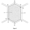
Figure 2 is a representation of the alignment of liquid crystal molecules in a stable state in a cavity of the device ofFigure 1 ; -
Figure 3 is a representation of the alignment of liquid crystal molecules in a different stable state in a cavity of the device ofFigure 1 ; -
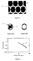
Figure 4 is a planar view of an alternate liquid crystal device; -
Figure 5(a) shows a stable state in a cavity of the device ofFigure 4 ; -
Figure 5(b) shows a differing stable state in a cavity of the device ofFigure 4 ; and -
Figure 6 shows the relationship between the magnitude of the switching voltage and the time the switching voltage is applied for in order to switch the device ofFigure 4 between stable states. - Containing liquid crystals within containment structures having certain shapes and dimensions can lead to the tendency of the liquid crystal molecules to arrange themselves into one of a multiple of stable states, each stable state having differing director structures and possibly different locations of regions of high distortion. A high distortion location is a region where the liquid crystal molecular order is significantly reduced compared to the bulk and a large elastic distortion occurs, as discussed by Repnik et al. in European Journal of Physics, Vol. 24, pages 481-492 (2003).
-
Figures 1(a) and (b) shows a reflective liquid crystal device having aliquid crystal material 10 contained within acontainment structure 20 that defines a plurality ofopenings 21. Thecontainment structure 20 is sandwiched between twotransparent substrates alignment layer preparations liquid crystal material 10. Thecontainment structure 20 and thesubstrates liquid crystal material 10. Theliquid crystal material 10 within each cavity completely fills it, so that the liquid crystal material is in direct contact with all of the cavity walls/surfaces, and adjacent cavities are completely isolated from each other. - A
polariser 50 is laminated to the outside of onetransparent substrate 30 and acolour filter 70 may be located over it. Thecolour filter 70 may be provided as a series of strips or squares of transparent coloured sections. Each cavity may have an area ofcolour filter 70 associated with it. Each colour filter may cover several cavities. Thecolour filter 70 may have red, green and blue transparent coloured sections. Laminated to thesubstrate 35 at the rear of the device is areflective layer 85 that acts as a reflective back plate. - As shown
Figures 2 and3 , the cavities of thecontainment structure 20 have an approximately hexagonal cross section having sharp orrounded corners transparent substrates - On their surfaces and facing the
liquid crystal 10, thetransparent substrates transparent electrodes electrodes transparent substrates - The cavities in the
containment structure 20 and associatedelectrodes electrodes - The alignment of the
liquid crystal molecules 10 on thecontainment structure 20 walls is dictated by a number of factors. For example, when thecontainment structure 20 is made of a polymeric material the polymer direction dictates the molecule direction. Alternatively, when a photoresist material such as SU8 is used to create thecontainment structure 20 the molecules prefer to lie in any direction parallel to the surface. As yet a further alternative, when a homeotropic alignment surface treatment is used the molecules prefer to lie perpendicular to the cavity surfaces with the molecules preferring parallel alignment at thetransparent substrates - As shown in
Figure 2 , for hexagonal cavities and for a planar alignment of theliquid crystal molecules 10 at the walls of thecontainment structure 20 and planar alignment at thetransparent substrates liquid crystal molecules 10 in the bulk of the region tend to align themselves at 45° to the sidewalls of the cavities and in a plane parallel to thetransparent substrates liquid crystal molecules 10,high distortion regions cavity corners liquid crystal molecules 10 in the region of thesehigh distortion sites liquid crystal molecules 10 in the bulk. The further a LC molecule is from the high distortion site, the more its orientation is similar to those of the bulk, i.e. at 45° to the walls of the cavity. - As shown in
Figure 3 , application of a suitable electric field having a component in the plane of the direction of theliquid crystal molecules 10 results in thehigh distortion regions corners corners bulk LC molecules 10 re-align themselves to match the change in location of the high distortion regions such that they lie at 45° to their previous direction but still lying in a plane parallel to that of thetransparent substrates liquid crystal molecules 10 always lie in a plane parallel to that of thesubstrates - Because the device of the present invention is reflective, in use the
light source 90 is located on the same side as theobserver 95. Light incident on the device is initially polarised by thepolariser 50 in a first direction. One of the possible stableliquid crystal 10 configurations is such that the polarisation direction of the light is rotated by 45° by the liquid crystal before it is reflected by thereflective element 85 and then rotated again by 45° by theliquid crystal 10. The total rotation of the polarisation of light by 90° means that the light is blocked by thepolariser 50. When a voltage is applied between the electrodes of a pixel, the bulk of the liquid crystal molecules can be switched by 45° into a second stable state, in which theliquid crystal molecules 10 are predominantly aligned with the direction of thepolariser 50.Light 90 incident on this second stable state is polarised, transmitted through the liquid crystal, reflected by thereflective element 85 and transmitted through the liquid crystal again with no change in polarisation direction. In this case, thepolariser 50 allows the light to be emitted and observed. In this way, the light is detected 95 or the picture viewed at the same side of the device as thelight source 90. - The sharpness of the corners of the cavity determines both the stability of the different states, where the high distortion regions are located at different corners, and the voltage needed to switch the device between states. For sharper corners the elastic energy barrier between two different molecular configurations is high compared to smoother corners. The increase in the energy barrier both increases the stability of the two states and increases the voltage needed to switch between the two states.
- The device in which the invention is embodied provides numerous advantages. The confinement of the liquid crystal into cavities means that the device is less susceptible than conventional arrangements to damage due to knocks and vibrations. In addition, altering the exact polygonal shape of the cavity allows the use of two stable uniform states that have identical energies. This allows easier switching between the two states.
- Using the invention, it is possible to achieve a rugged device having a good contrast and reflectivity, a wide range of viewing angles with good optical characteristics, a range of greyscales or full colour, 45° rotation of light between states and low power consumption. These properties make the present invention particularly useful in optical switches, liquid crystal displays and variable phase gratings. Liquid crystal displays in accordance with the present invention are particularly suitable as electronic paper or displays in portable devices due to the good contrast, wide viewing angle, low power consumption and their ability to use passive addressing and therefore allow the use of significantly more pixels than in current devices.
- Although the above device advantageously isolates the contents of each cavity, in some situations it may be preferable to allow fluid communication between cavities, for example to aid filling of the cavities with liquid crystal material. Thus, in an alternative embodiment as shown in
Figure 4 , two or more of the cavities are linked by at least onechannel 180. As the size of thechannel 180 increases, the elastic preference of theliquid crystal 10 to be oriented and aligned in the direction of thechannel 180 increases. If thechannel 180 is too wide, then the stability of the stable state in which theliquid crystal 10 aligns perpendicular to thechannels 180 is decreased, potentially to the point that this state is no longer stable. In addition, thechannel 180 may affect the optics of the device. Therefore, in order to minimise these effects, eachchannel 180 is advantageously less than 20µm wide and preferably less than 5µm wide. - As an alternative embodiment, the above channel alignment effect may be advantageously utilised by sizing and positioning the
channels 180 to provide at least one additional stable state. Depending on the orientation of thepolariser 50 and position of thechannels 180, the additional state may be a "grey" state rather than just light or dark. -
Figures 5(a) and 5(b) respectively show two differing stable states in a cavity of the device ofFigure 4 . The liquid crystal molecules in the cavity shown inFigure 5(a) are oriented with the polarisation direction of thepolariser 50 whilst the liquid crystal molecules shown inFigure 5(b) are oriented at 45° to the liquid crystal shown inFigure 5(a) . In this example, the cavity has a horizontal extent of 80µm and is placed under crossed polarisers. It can be seen that the stable state ofFigure 5(a) is blacker than the stable state ofFigure 5(b) . - Switching of the above devices depends on the time that the switching field is applied for and the maximum applied voltage. An example of this is shown in
Figure 6 , which shows switching by applying a 10kHz electric field for different lengths of time and with maximum applied voltages. Operation of the device in the region above theline 190 results in switching between stable states, whilst below theline 190, there is no switching. As can be seen, the shorter the time that the switching field is applied for, the higher the maximum applied voltage required to achieve switching and vice-versa. - A skilled person will appreciate that variations of the disclosed arrangements are possible without departing from the invention. For example, in order to minimise diffraction effects, the cavities within the
containment structure 20 may be randomly arranged. Alternately, if diffraction effects are required, the cavities can be arranged in orderly fashion, such as an M by N grid, so as to achieve the required diffraction effect, as is known in the art. Furthermore, whilst in the device described with reference toFigures 2 to 4 , a planar alignment exists on the walls of the cavities and the material of thetransparent substrates
Claims (16)
- A reflective multistable liquid crystal device having liquid crystal molecules (10) between two substrates in one or more cavities (20) having a polygon shape in cross-section, the liquid crystal molecules being in direct contact with each cavity, wherein at least one liquid crystal region (100,110) of high distortion is formed at a corner (120,130,140,150, 160,170) in each cavity, the distortion region(s) having at least two stable states of distortion, the device having an entrance polarizer and the device is configured with electrodes arranged to apply an electric field having a component substantially parallel to the substrates whereby the distortion region is switchable between the at least two stable states with an oblique angle of rotation between the direction of the liquid crystal molecules in the bulk of the liquid crystal in the at least two stable states.
- A multistable liquid crystal device as claimed in claim 1 wherein the liquid crystal molecules and the cavities are between a transparent substrate and a reflective substrate.
- A multistable liquid crystal device according to clam 1 or claim 2 wherein the majority of liquid crystal molecules in at least one stable state are aligned at an oblique angle to the direction of the majority of liquid crystal molecules in at least one other stable state, wherein the majority of liquid crystal molecules in at least one stable state are aligned at substantially 45° to the direction of the majority of liquid crystal molecules in at least one other stable state.
- A multistable liquid crystal device according to any of the preceding claims wherein the one or more cavities have a hexagonal cross section.
- A multistable liquid crystal device according to any of the preceding claims wherein there is a sharp transition between certain adjoining cavity walls.
- A multistable liquid crystal device according to any of the preceding claims
wherein the walls that define the cavities are substantially perpendicular to a base or substrate. - A multistable liquid device according to any of the preceding claims wherein the high distortion regions are located at corners of the cavities.
- A multistable liquid crystal device according to any of the preceding claims wherein the liquid crystal molecules in the stable states lie in a plane substantially parallel to a base of the cavity.
- A multistable liquid crystal device according to any of the preceding claims wherein the liquid crystal in each cavity is isolated from the liquid crystal in adjoining cavities.
- A multistable liquid crystal device according to any of claims 1 to 9, wherein at least two cavities are linked by at least one channel, optionally wherein the channel(s) 180 are less than 20 µm wide and preferably less than 5µm wide.
- A multistable liquid crystal device according to any of the preceding claims where the liquid crystal device is a nematic liquid crystal device.
- A multistable liquid crystal device according to any of the preceding claims wherein electrodes are located on the cavity walls.
- A multistable liquid crystal device according to any of the preceding claims where the containment structure is formed from a photoresist or polymeric material.
- A multistable liquid crystal device according to any of the preceding claims where at least one electrode is associated with one or more cavities, and attached to a switching device, optionally wherein the switching device contains one or more thin film transistors.
- An optical switch or a changeable phase grating or a phase device for telecommunications or a display device that includes a multistable liquid crystal device according to any of claims 1 to 16.
- A method of switching states in a liquid crystal device containing liquid crystal molecules within a cavity in a containment structure, as claimed in any of claims 1 to 15.
Priority Applications (3)
| Application Number | Priority Date | Filing Date | Title |
|---|---|---|---|
| SI200731168T SI2024784T1 (en) | 2006-06-07 | 2007-06-07 | Multistable reflective liquid crystal device |
| PL07733096T PL2024784T3 (en) | 2006-06-07 | 2007-06-07 | Multistable reflective liquid crystal device |
| CY20131100177T CY1113721T1 (en) | 2006-06-07 | 2013-02-26 | POLYSTHATIC REFLECTIVE LIQUID CRYSTAL Layout |
Applications Claiming Priority (2)
| Application Number | Priority Date | Filing Date | Title |
|---|---|---|---|
| GBGB0611141.3A GB0611141D0 (en) | 2006-06-07 | 2006-06-07 | Multistable reflective liquid crystal device |
| PCT/GB2007/002084 WO2007141525A1 (en) | 2006-06-07 | 2007-06-07 | Multistable reflective liquid crystal device |
Publications (2)
| Publication Number | Publication Date |
|---|---|
| EP2024784A1 EP2024784A1 (en) | 2009-02-18 |
| EP2024784B1 true EP2024784B1 (en) | 2012-12-05 |
Family
ID=36745337
Family Applications (1)
| Application Number | Title | Priority Date | Filing Date |
|---|---|---|---|
| EP07733096A Not-in-force EP2024784B1 (en) | 2006-06-07 | 2007-06-07 | Multistable reflective liquid crystal device |
Country Status (14)
| Country | Link |
|---|---|
| US (1) | US9280018B2 (en) |
| EP (1) | EP2024784B1 (en) |
| JP (1) | JP2009540348A (en) |
| KR (1) | KR101464497B1 (en) |
| CN (1) | CN101467096A (en) |
| CY (1) | CY1113721T1 (en) |
| DK (1) | DK2024784T3 (en) |
| ES (1) | ES2399925T3 (en) |
| GB (1) | GB0611141D0 (en) |
| PL (1) | PL2024784T3 (en) |
| PT (1) | PT2024784E (en) |
| SI (1) | SI2024784T1 (en) |
| TW (1) | TW200807074A (en) |
| WO (1) | WO2007141525A1 (en) |
Families Citing this family (21)
| Publication number | Priority date | Publication date | Assignee | Title |
|---|---|---|---|---|
| FR2897164B1 (en) | 2006-02-09 | 2008-03-14 | Commissariat Energie Atomique | REALIZING CAVITIES THAT CAN BE FILLED BY A FLUID MATERIAL IN AN OPTICAL MICROTECHNOLOGICAL COMPOUND |
| CN101533162B (en) * | 2008-03-14 | 2011-09-07 | 苏州汉朗光电有限公司 | Electrical control light modulating medium |
| FR2929715B1 (en) | 2008-04-04 | 2010-09-10 | Commissariat Energie Atomique | METHOD FOR PRODUCING MICRONIC OR SUBMICRONIC CAVITIES |
| FR2933205B1 (en) | 2008-06-27 | 2010-08-13 | Commissariat Energie Atomique | IMPROVED METHOD FOR MAKING LIQUID-FILLED ENCLOSURES AND CLOSED BY A MEMBRANE |
| FR2934061B1 (en) * | 2008-07-15 | 2010-10-15 | Commissariat Energie Atomique | LIQUID CRYSTAL ALIGNMENT LAYER DEPOSITED AND FRICTED BEFORE REALIZING THE MICROSTRUCTURES |
| FR2963112B1 (en) | 2010-07-21 | 2013-02-15 | Commissariat Energie Atomique | WALL MICROSTRUCTURE WITH DETERMINED OPTICAL PROPERTIES AND METHOD FOR PRODUCING MICROSTRUCTURES |
| JP2014219637A (en) * | 2013-05-10 | 2014-11-20 | 大日本印刷株式会社 | Reflective display device |
| KR101644902B1 (en) | 2013-05-30 | 2016-08-03 | 삼성디스플레이 주식회사 | Display device and manufacturing method thereof |
| KR20150008758A (en) | 2013-07-15 | 2015-01-23 | 삼성디스플레이 주식회사 | Liquid crystal display device and manufacturing method thereof |
| KR20150019323A (en) | 2013-08-13 | 2015-02-25 | 삼성디스플레이 주식회사 | Liquid crystal display and method of manufacturing the same |
| KR101668381B1 (en) * | 2013-09-30 | 2016-10-31 | 삼성디스플레이 주식회사 | Liquid crystal display and method of manufacturing the same |
| KR20150066977A (en) | 2013-12-09 | 2015-06-17 | 삼성디스플레이 주식회사 | Liquid crystal display and method of manufacturing the same |
| KR20150115123A (en) | 2014-04-02 | 2015-10-14 | 삼성디스플레이 주식회사 | Display device and manufacturing method thereof |
| KR20150122899A (en) * | 2014-04-23 | 2015-11-03 | 삼성디스플레이 주식회사 | Display device and manufacturing method thereof |
| US10451941B2 (en) * | 2014-09-30 | 2019-10-22 | Samsung Display Co., Ltd. | Liquid crystal display and method of manufacturing the same |
| KR20160068112A (en) * | 2014-12-04 | 2016-06-15 | 삼성디스플레이 주식회사 | Display device and manufacturing method thereof |
| WO2016150393A1 (en) * | 2015-03-24 | 2016-09-29 | The Hong Kong University Of Science And Technology | Optically addressed multi-stable full color liquid crystal display |
| KR20170046879A (en) * | 2015-10-21 | 2017-05-04 | 삼성디스플레이 주식회사 | Display device |
| WO2019203612A1 (en) * | 2018-04-20 | 2019-10-24 | 주식회사 엘지화학 | Variable transmittance film and smart window including same |
| US10670910B2 (en) | 2018-09-24 | 2020-06-02 | Sharp Kabushiki Kaisha | LCD with four stable and optically distinct states |
| US10698284B2 (en) | 2018-09-24 | 2020-06-30 | Sharp Kabushiki Kaisha | ZBD liquid crystal device and methods of operating such device |
Family Cites Families (15)
| Publication number | Priority date | Publication date | Assignee | Title |
|---|---|---|---|---|
| JPS5528004A (en) * | 1978-08-18 | 1980-02-28 | Canon Inc | Liquid crystal display element |
| US4333708A (en) * | 1979-11-30 | 1982-06-08 | Bell Telephone Laboratories, Incorporated | Mechanically multistable liquid crystal cell |
| FR2666908B2 (en) | 1990-01-30 | 1992-12-18 | Centre Nat Rech Scient | IMPROVEMENTS ON BISTABLE OPTICAL DEVICES WITH LIQUID CRYSTALS AND ELECTROCHIRAL CONTROL. |
| FR2666923A2 (en) | 1990-06-22 | 1992-03-20 | Centre Nat Rech Scient | Improvements to nematic liquid-crystal displays, with surface bistability, controlled by flexoelectric effect |
| DE69427671T2 (en) * | 1993-10-19 | 2002-05-08 | Sharp Kk | Liquid crystal display device and its manufacturing method |
| GB9402513D0 (en) | 1994-02-09 | 1994-03-30 | Secr Defence | Bistable nematic liquid crystal device |
| GB9521106D0 (en) | 1995-10-16 | 1995-12-20 | Secr Defence | Bistable nematic liquid crystal device |
| GB2347005B (en) * | 1996-07-26 | 2000-10-04 | Sharp Kk | Methods of filling liquid crystal device |
| GB2321718A (en) * | 1997-01-31 | 1998-08-05 | Nat Science Council | LIquid crystal display |
| KR19980033500A (en) | 1998-04-18 | 1998-07-25 | 이신두 | Reflective bistable nematic liquid crystal display |
| GB9928126D0 (en) * | 1999-11-30 | 2000-01-26 | Secr Defence | Bistable nematic liquid crystal device |
| EP1139151B1 (en) | 2000-03-27 | 2007-05-16 | Hewlett-Packard Company, A Delaware Corporation | Bistable nematic liquid crystal device |
| EP1271225A1 (en) | 2001-06-22 | 2003-01-02 | Hewlett-Packard Company, A Delaware Corporation | Bistable nematic liquid crystal device |
| EP1271226B1 (en) * | 2001-06-22 | 2007-04-04 | Hewlett-Packard Company | Bistable nematic liquid crystal device |
| GB0426582D0 (en) * | 2004-12-03 | 2005-01-05 | Univ Strathclyde | Bistable liquid crystal device |
-
2006
- 2006-06-07 GB GBGB0611141.3A patent/GB0611141D0/en not_active Ceased
-
2007
- 2007-06-06 TW TW096120293A patent/TW200807074A/en unknown
- 2007-06-07 WO PCT/GB2007/002084 patent/WO2007141525A1/en not_active Ceased
- 2007-06-07 DK DK07733096.7T patent/DK2024784T3/en active
- 2007-06-07 EP EP07733096A patent/EP2024784B1/en not_active Not-in-force
- 2007-06-07 JP JP2009513763A patent/JP2009540348A/en active Pending
- 2007-06-07 CN CNA2007800212893A patent/CN101467096A/en active Pending
- 2007-06-07 PT PT77330967T patent/PT2024784E/en unknown
- 2007-06-07 US US12/308,142 patent/US9280018B2/en not_active Expired - Fee Related
- 2007-06-07 ES ES07733096T patent/ES2399925T3/en active Active
- 2007-06-07 SI SI200731168T patent/SI2024784T1/en unknown
- 2007-06-07 PL PL07733096T patent/PL2024784T3/en unknown
-
2008
- 2008-12-04 KR KR1020087029728A patent/KR101464497B1/en not_active Expired - Fee Related
-
2013
- 2013-02-26 CY CY20131100177T patent/CY1113721T1/en unknown
Also Published As
| Publication number | Publication date |
|---|---|
| GB0611141D0 (en) | 2006-07-19 |
| CY1113721T1 (en) | 2016-06-22 |
| WO2007141525A1 (en) | 2007-12-13 |
| US20100014011A1 (en) | 2010-01-21 |
| ES2399925T3 (en) | 2013-04-04 |
| JP2009540348A (en) | 2009-11-19 |
| EP2024784A1 (en) | 2009-02-18 |
| TW200807074A (en) | 2008-02-01 |
| SI2024784T1 (en) | 2013-04-30 |
| DK2024784T3 (en) | 2013-02-18 |
| PL2024784T3 (en) | 2013-04-30 |
| PT2024784E (en) | 2013-03-11 |
| US9280018B2 (en) | 2016-03-08 |
| CN101467096A (en) | 2009-06-24 |
| KR101464497B1 (en) | 2014-12-04 |
| KR20090026142A (en) | 2009-03-11 |
Similar Documents
| Publication | Publication Date | Title |
|---|---|---|
| US9280018B2 (en) | Multistable reflective liquid crystal device | |
| US7145624B2 (en) | Liquid crystal display device having multiple domains with radially inclined LC molecules | |
| CN100437266C (en) | Polarization rotator, parallax barrier, display and optical modulator | |
| US5568287A (en) | Liquid crystal device with optical means of high refractive index at pixels and low refractive index between pixels | |
| KR19990056726A (en) | LCD | |
| US20110170040A1 (en) | Liquid crystal display | |
| KR101888516B1 (en) | Dual mode liquid crystal display device | |
| US6690440B1 (en) | Liquid crystal element and manufacturing method thereof | |
| US20020089479A1 (en) | Liquid crystal display device | |
| US9007548B2 (en) | Wide view angle liquid crystal display device operating in normally white mode | |
| JP2002169155A (en) | Liquid crystal display device | |
| US20080106662A1 (en) | Bistable Liquid Crystal Device | |
| JP2000171831A (en) | LCD panel | |
| KR100224699B1 (en) | LCD | |
| RU2393517C2 (en) | Passive-matrix lcd and method of its control | |
| EP1927885B1 (en) | Multistable liquid crystal device | |
| WO1993023788A1 (en) | Display devices | |
| KR20010098550A (en) | Liquid crystal display (lcd) having improved isocontrast performance and method for producing same | |
| KR100674231B1 (en) | Fringe Field Drive Mode Liquid Crystal Display | |
| JP2002040476A (en) | Liquid crystal display device | |
| KR20010038825A (en) | transflective type liquid crystal display device. | |
| KR20040099911A (en) | In plane switching mode liquid crystal display device and fabrication method thereof |
Legal Events
| Date | Code | Title | Description |
|---|---|---|---|
| PUAI | Public reference made under article 153(3) epc to a published international application that has entered the european phase |
Free format text: ORIGINAL CODE: 0009012 |
|
| 17P | Request for examination filed |
Effective date: 20081121 |
|
| AK | Designated contracting states |
Kind code of ref document: A1 Designated state(s): AT BE BG CH CY CZ DE DK EE ES FI FR GB GR HU IE IS IT LI LT LU LV MC MT NL PL PT RO SE SI SK TR |
|
| AX | Request for extension of the european patent |
Extension state: AL BA HR MK RS |
|
| 17Q | First examination report despatched |
Effective date: 20110217 |
|
| RAP1 | Party data changed (applicant data changed or rights of an application transferred) |
Owner name: SYBRE LIMITED |
|
| RAP1 | Party data changed (applicant data changed or rights of an application transferred) |
Owner name: ZINK TECHNOLOGIES LIMITED |
|
| GRAC | Information related to communication of intention to grant a patent modified |
Free format text: ORIGINAL CODE: EPIDOSCIGR1 |
|
| GRAP | Despatch of communication of intention to grant a patent |
Free format text: ORIGINAL CODE: EPIDOSNIGR1 |
|
| GRAC | Information related to communication of intention to grant a patent modified |
Free format text: ORIGINAL CODE: EPIDOSCIGR1 |
|
| DAX | Request for extension of the european patent (deleted) | ||
| GRAC | Information related to communication of intention to grant a patent modified |
Free format text: ORIGINAL CODE: EPIDOSCIGR1 |
|
| GRAC | Information related to communication of intention to grant a patent modified |
Free format text: ORIGINAL CODE: EPIDOSCIGR1 |
|
| GRAS | Grant fee paid |
Free format text: ORIGINAL CODE: EPIDOSNIGR3 |
|
| GRAA | (expected) grant |
Free format text: ORIGINAL CODE: 0009210 |
|
| AK | Designated contracting states |
Kind code of ref document: B1 Designated state(s): AT BE BG CH CY CZ DE DK EE ES FI FR GB GR HU IE IS IT LI LT LU LV MC MT NL PL PT RO SE SI SK TR |
|
| REG | Reference to a national code |
Ref country code: GB Ref legal event code: FG4D |
|
| REG | Reference to a national code |
Ref country code: CH Ref legal event code: EP |
|
| REG | Reference to a national code |
Ref country code: AT Ref legal event code: REF Ref document number: 587566 Country of ref document: AT Kind code of ref document: T Effective date: 20121215 |
|
| REG | Reference to a national code |
Ref country code: IE Ref legal event code: FG4D |
|
| REG | Reference to a national code |
Ref country code: DE Ref legal event code: R096 Ref document number: 602007027139 Country of ref document: DE Effective date: 20130131 |
|
| REG | Reference to a national code |
Ref country code: DK Ref legal event code: T3 |
|
| REG | Reference to a national code |
Ref country code: RO Ref legal event code: EPE |
|
| REG | Reference to a national code |
Ref country code: PT Ref legal event code: SC4A Free format text: AVAILABILITY OF NATIONAL TRANSLATION Effective date: 20130301 |
|
| REG | Reference to a national code |
Ref country code: SE Ref legal event code: TRGR |
|
| REG | Reference to a national code |
Ref country code: NL Ref legal event code: T3 |
|
| REG | Reference to a national code |
Ref country code: ES Ref legal event code: FG2A Ref document number: 2399925 Country of ref document: ES Kind code of ref document: T3 Effective date: 20130404 |
|
| REG | Reference to a national code |
Ref country code: PL Ref legal event code: T3 |
|
| REG | Reference to a national code |
Ref country code: GR Ref legal event code: EP Ref document number: 20130400346 Country of ref document: GR Effective date: 20130327 |
|
| REG | Reference to a national code |
Ref country code: SK Ref legal event code: T3 Ref document number: E 13594 Country of ref document: SK |
|
| REG | Reference to a national code |
Ref country code: EE Ref legal event code: FG4A Ref document number: E007908 Country of ref document: EE Effective date: 20130301 |
|
| PGFP | Annual fee paid to national office [announced via postgrant information from national office to epo] |
Ref country code: SE Payment date: 20130627 Year of fee payment: 7 Ref country code: IS Payment date: 20130624 Year of fee payment: 7 Ref country code: EE Payment date: 20130626 Year of fee payment: 7 Ref country code: DK Payment date: 20130627 Year of fee payment: 7 Ref country code: MC Payment date: 20130621 Year of fee payment: 7 Ref country code: LU Payment date: 20130628 Year of fee payment: 7 Ref country code: IE Payment date: 20130627 Year of fee payment: 7 |
|
| PGFP | Annual fee paid to national office [announced via postgrant information from national office to epo] |
Ref country code: FI Payment date: 20130624 Year of fee payment: 7 Ref country code: GR Payment date: 20130627 Year of fee payment: 7 Ref country code: LV Payment date: 20130625 Year of fee payment: 7 |
|
| PGFP | Annual fee paid to national office [announced via postgrant information from national office to epo] |
Ref country code: BG Payment date: 20130625 Year of fee payment: 7 Ref country code: BE Payment date: 20130627 Year of fee payment: 7 |
|
| REG | Reference to a national code |
Ref country code: HU Ref legal event code: AG4A Ref document number: E016624 Country of ref document: HU |
|
| PLBE | No opposition filed within time limit |
Free format text: ORIGINAL CODE: 0009261 |
|
| STAA | Information on the status of an ep patent application or granted ep patent |
Free format text: STATUS: NO OPPOSITION FILED WITHIN TIME LIMIT |
|
| PGFP | Annual fee paid to national office [announced via postgrant information from national office to epo] |
Ref country code: CH Payment date: 20130710 Year of fee payment: 7 Ref country code: PT Payment date: 20130301 Year of fee payment: 7 Ref country code: HU Payment date: 20130729 Year of fee payment: 7 Ref country code: LT Payment date: 20130712 Year of fee payment: 7 Ref country code: RO Payment date: 20130722 Year of fee payment: 7 Ref country code: SI Payment date: 20130712 Year of fee payment: 7 Ref country code: NL Payment date: 20130627 Year of fee payment: 7 Ref country code: CZ Payment date: 20130712 Year of fee payment: 7 |
|
| 26N | No opposition filed |
Effective date: 20130906 |
|
| PGFP | Annual fee paid to national office [announced via postgrant information from national office to epo] |
Ref country code: TR Payment date: 20130711 Year of fee payment: 7 Ref country code: PL Payment date: 20130712 Year of fee payment: 7 |
|
| REG | Reference to a national code |
Ref country code: DE Ref legal event code: R097 Ref document number: 602007027139 Country of ref document: DE Effective date: 20130906 |
|
| PGFP | Annual fee paid to national office [announced via postgrant information from national office to epo] |
Ref country code: SK Payment date: 20131030 Year of fee payment: 7 Ref country code: CY Payment date: 20130723 Year of fee payment: 7 |
|
| REG | Reference to a national code |
Ref country code: PT Ref legal event code: MM4A Free format text: LAPSE DUE TO NON-PAYMENT OF FEES Effective date: 20141209 |
|
| REG | Reference to a national code |
Ref country code: DK Ref legal event code: EBP Effective date: 20140630 |
|
| REG | Reference to a national code |
Ref country code: NL Ref legal event code: V1 Effective date: 20150101 |
|
| REG | Reference to a national code |
Ref country code: LT Ref legal event code: MM4D Effective date: 20140607 |
|
| PG25 | Lapsed in a contracting state [announced via postgrant information from national office to epo] |
Ref country code: CZ Free format text: LAPSE BECAUSE OF NON-PAYMENT OF DUE FEES Effective date: 20140607 Ref country code: SE Free format text: LAPSE BECAUSE OF NON-PAYMENT OF DUE FEES Effective date: 20140608 Ref country code: LT Free format text: LAPSE BECAUSE OF NON-PAYMENT OF DUE FEES Effective date: 20140607 Ref country code: PT Free format text: LAPSE BECAUSE OF NON-PAYMENT OF DUE FEES Effective date: 20141209 Ref country code: FI Free format text: LAPSE BECAUSE OF NON-PAYMENT OF DUE FEES Effective date: 20140607 Ref country code: LU Free format text: LAPSE BECAUSE OF NON-PAYMENT OF DUE FEES Effective date: 20140607 Ref country code: MC Free format text: LAPSE BECAUSE OF NON-PAYMENT OF DUE FEES Effective date: 20140630 Ref country code: RO Free format text: LAPSE BECAUSE OF NON-PAYMENT OF DUE FEES Effective date: 20140607 |
|
| PGFP | Annual fee paid to national office [announced via postgrant information from national office to epo] |
Ref country code: ES Payment date: 20141120 Year of fee payment: 8 Ref country code: FR Payment date: 20141119 Year of fee payment: 8 Ref country code: GB Payment date: 20141113 Year of fee payment: 8 Ref country code: DE Payment date: 20141119 Year of fee payment: 8 |
|
| REG | Reference to a national code |
Ref country code: CH Ref legal event code: PL |
|
| REG | Reference to a national code |
Ref country code: SE Ref legal event code: EUG |
|
| REG | Reference to a national code |
Ref country code: AT Ref legal event code: MM01 Ref document number: 587566 Country of ref document: AT Kind code of ref document: T Effective date: 20140607 |
|
| REG | Reference to a national code |
Ref country code: EE Ref legal event code: MM4A Ref document number: E007908 Country of ref document: EE Effective date: 20140630 |
|
| PG25 | Lapsed in a contracting state [announced via postgrant information from national office to epo] |
Ref country code: IS Free format text: LAPSE BECAUSE OF FAILURE TO SUBMIT A TRANSLATION OF THE DESCRIPTION OR TO PAY THE FEE WITHIN THE PRESCRIBED TIME-LIMIT Effective date: 20141231 Ref country code: LV Free format text: LAPSE BECAUSE OF NON-PAYMENT OF DUE FEES Effective date: 20140607 Ref country code: CY Free format text: LAPSE BECAUSE OF NON-PAYMENT OF DUE FEES Effective date: 20140607 |
|
| PGFP | Annual fee paid to national office [announced via postgrant information from national office to epo] |
Ref country code: MT Payment date: 20130715 Year of fee payment: 7 |
|
| REG | Reference to a national code |
Ref country code: SK Ref legal event code: MM4A Ref document number: E 13594 Country of ref document: SK Effective date: 20140607 |
|
| REG | Reference to a national code |
Ref country code: GR Ref legal event code: ML Ref document number: 20130400346 Country of ref document: GR Effective date: 20150105 |
|
| REG | Reference to a national code |
Ref country code: IE Ref legal event code: MM4A |
|
| PG25 | Lapsed in a contracting state [announced via postgrant information from national office to epo] |
Ref country code: NL Free format text: LAPSE BECAUSE OF NON-PAYMENT OF DUE FEES Effective date: 20150101 |
|
| PGFP | Annual fee paid to national office [announced via postgrant information from national office to epo] |
Ref country code: IT Payment date: 20141126 Year of fee payment: 8 |
|
| REG | Reference to a national code |
Ref country code: SI Ref legal event code: KO00 Effective date: 20150216 |
|
| PG25 | Lapsed in a contracting state [announced via postgrant information from national office to epo] |
Ref country code: LI Free format text: LAPSE BECAUSE OF NON-PAYMENT OF DUE FEES Effective date: 20140630 Ref country code: IE Free format text: LAPSE BECAUSE OF NON-PAYMENT OF DUE FEES Effective date: 20140607 Ref country code: BG Free format text: LAPSE BECAUSE OF NON-PAYMENT OF DUE FEES Effective date: 20150331 Ref country code: EE Free format text: LAPSE BECAUSE OF NON-PAYMENT OF DUE FEES Effective date: 20140630 Ref country code: SK Free format text: LAPSE BECAUSE OF NON-PAYMENT OF DUE FEES Effective date: 20140607 Ref country code: CH Free format text: LAPSE BECAUSE OF NON-PAYMENT OF DUE FEES Effective date: 20140630 Ref country code: HU Free format text: LAPSE BECAUSE OF NON-PAYMENT OF DUE FEES Effective date: 20140608 |
|
| PG25 | Lapsed in a contracting state [announced via postgrant information from national office to epo] |
Ref country code: GR Free format text: LAPSE BECAUSE OF NON-PAYMENT OF DUE FEES Effective date: 20150105 Ref country code: SI Free format text: LAPSE BECAUSE OF NON-PAYMENT OF DUE FEES Effective date: 20140608 Ref country code: AT Free format text: LAPSE BECAUSE OF NON-PAYMENT OF DUE FEES Effective date: 20140607 |
|
| PG25 | Lapsed in a contracting state [announced via postgrant information from national office to epo] |
Ref country code: DK Free format text: LAPSE BECAUSE OF NON-PAYMENT OF DUE FEES Effective date: 20140630 |
|
| REG | Reference to a national code |
Ref country code: PL Ref legal event code: LAPE |
|
| PG25 | Lapsed in a contracting state [announced via postgrant information from national office to epo] |
Ref country code: PL Free format text: LAPSE BECAUSE OF NON-PAYMENT OF DUE FEES Effective date: 20140607 |
|
| REG | Reference to a national code |
Ref country code: DE Ref legal event code: R119 Ref document number: 602007027139 Country of ref document: DE |
|
| PG25 | Lapsed in a contracting state [announced via postgrant information from national office to epo] |
Ref country code: IT Free format text: LAPSE BECAUSE OF NON-PAYMENT OF DUE FEES Effective date: 20150607 |
|
| GBPC | Gb: european patent ceased through non-payment of renewal fee |
Effective date: 20150607 |
|
| PG25 | Lapsed in a contracting state [announced via postgrant information from national office to epo] |
Ref country code: MT Free format text: LAPSE BECAUSE OF NON-PAYMENT OF DUE FEES Effective date: 20140630 |
|
| REG | Reference to a national code |
Ref country code: FR Ref legal event code: ST Effective date: 20160229 |
|
| PG25 | Lapsed in a contracting state [announced via postgrant information from national office to epo] |
Ref country code: DE Free format text: LAPSE BECAUSE OF NON-PAYMENT OF DUE FEES Effective date: 20160101 Ref country code: GB Free format text: LAPSE BECAUSE OF NON-PAYMENT OF DUE FEES Effective date: 20150607 |
|
| PG25 | Lapsed in a contracting state [announced via postgrant information from national office to epo] |
Ref country code: FR Free format text: LAPSE BECAUSE OF NON-PAYMENT OF DUE FEES Effective date: 20150630 |
|
| REG | Reference to a national code |
Ref country code: ES Ref legal event code: FD2A Effective date: 20161202 |
|
| PG25 | Lapsed in a contracting state [announced via postgrant information from national office to epo] |
Ref country code: ES Free format text: LAPSE BECAUSE OF NON-PAYMENT OF DUE FEES Effective date: 20150608 |
|
| PG25 | Lapsed in a contracting state [announced via postgrant information from national office to epo] |
Ref country code: BE Free format text: LAPSE BECAUSE OF NON-PAYMENT OF DUE FEES Effective date: 20140630 |
|
| PG25 | Lapsed in a contracting state [announced via postgrant information from national office to epo] |
Ref country code: TR Free format text: LAPSE BECAUSE OF NON-PAYMENT OF DUE FEES Effective date: 20140607 |
|
| PG25 | Lapsed in a contracting state [announced via postgrant information from national office to epo] |
Ref country code: MT Free format text: LAPSE BECAUSE OF NON-PAYMENT OF DUE FEES Effective date: 20140607 |