EP2023396A1 - Display device - Google Patents
Display device Download PDFInfo
- Publication number
- EP2023396A1 EP2023396A1 EP08252383A EP08252383A EP2023396A1 EP 2023396 A1 EP2023396 A1 EP 2023396A1 EP 08252383 A EP08252383 A EP 08252383A EP 08252383 A EP08252383 A EP 08252383A EP 2023396 A1 EP2023396 A1 EP 2023396A1
- Authority
- EP
- European Patent Office
- Prior art keywords
- display device
- pixel electrode
- light emitting
- layer
- electrode
- Prior art date
- Legal status (The legal status is an assumption and is not a legal conclusion. Google has not performed a legal analysis and makes no representation as to the accuracy of the status listed.)
- Granted
Links
Images

Classifications
-
- H—ELECTRICITY
- H05—ELECTRIC TECHNIQUES NOT OTHERWISE PROVIDED FOR
- H05B—ELECTRIC HEATING; ELECTRIC LIGHT SOURCES NOT OTHERWISE PROVIDED FOR; CIRCUIT ARRANGEMENTS FOR ELECTRIC LIGHT SOURCES, IN GENERAL
- H05B33/00—Electroluminescent light sources
- H05B33/12—Light sources with substantially two-dimensional [2D] radiating surfaces
- H05B33/22—Light sources with substantially two-dimensional [2D] radiating surfaces characterised by the chemical or physical composition or the arrangement of auxiliary dielectric or reflective layers
-
- G—PHYSICS
- G02—OPTICS
- G02F—OPTICAL DEVICES OR ARRANGEMENTS FOR THE CONTROL OF LIGHT BY MODIFICATION OF THE OPTICAL PROPERTIES OF THE MEDIA OF THE ELEMENTS INVOLVED THEREIN; NON-LINEAR OPTICS; FREQUENCY-CHANGING OF LIGHT; OPTICAL LOGIC ELEMENTS; OPTICAL ANALOGUE/DIGITAL CONVERTERS
- G02F1/00—Devices or arrangements for the control of the intensity, colour, phase, polarisation or direction of light arriving from an independent light source, e.g. switching, gating or modulating; Non-linear optics
- G02F1/01—Devices or arrangements for the control of the intensity, colour, phase, polarisation or direction of light arriving from an independent light source, e.g. switching, gating or modulating; Non-linear optics for the control of the intensity, phase, polarisation or colour
- G02F1/13—Devices or arrangements for the control of the intensity, colour, phase, polarisation or direction of light arriving from an independent light source, e.g. switching, gating or modulating; Non-linear optics for the control of the intensity, phase, polarisation or colour based on liquid crystals, e.g. single liquid crystal display cells
- G02F1/1323—Arrangements for providing a switchable viewing angle
-
- H—ELECTRICITY
- H10—SEMICONDUCTOR DEVICES; ELECTRIC SOLID-STATE DEVICES NOT OTHERWISE PROVIDED FOR
- H10K—ORGANIC ELECTRIC SOLID-STATE DEVICES
- H10K59/00—Integrated devices, or assemblies of multiple devices, comprising at least one organic light-emitting element covered by group H10K50/00
- H10K59/10—OLED displays
- H10K59/12—Active-matrix OLED [AMOLED] displays
-
- H—ELECTRICITY
- H10—SEMICONDUCTOR DEVICES; ELECTRIC SOLID-STATE DEVICES NOT OTHERWISE PROVIDED FOR
- H10K—ORGANIC ELECTRIC SOLID-STATE DEVICES
- H10K59/00—Integrated devices, or assemblies of multiple devices, comprising at least one organic light-emitting element covered by group H10K50/00
- H10K59/50—OLEDs integrated with light modulating elements, e.g. with electrochromic elements, photochromic elements or liquid crystal elements
-
- G—PHYSICS
- G02—OPTICS
- G02F—OPTICAL DEVICES OR ARRANGEMENTS FOR THE CONTROL OF LIGHT BY MODIFICATION OF THE OPTICAL PROPERTIES OF THE MEDIA OF THE ELEMENTS INVOLVED THEREIN; NON-LINEAR OPTICS; FREQUENCY-CHANGING OF LIGHT; OPTICAL LOGIC ELEMENTS; OPTICAL ANALOGUE/DIGITAL CONVERTERS
- G02F2201/00—Constructional arrangements not provided for in groups G02F1/00 - G02F7/00
- G02F2201/44—Arrangements combining different electro-active layers, e.g. electrochromic, liquid crystal or electroluminescent layers
-
- H—ELECTRICITY
- H10—SEMICONDUCTOR DEVICES; ELECTRIC SOLID-STATE DEVICES NOT OTHERWISE PROVIDED FOR
- H10K—ORGANIC ELECTRIC SOLID-STATE DEVICES
- H10K50/00—Organic light-emitting devices
- H10K50/80—Constructional details
- H10K50/85—Arrangements for extracting light from the devices
-
- H—ELECTRICITY
- H10—SEMICONDUCTOR DEVICES; ELECTRIC SOLID-STATE DEVICES NOT OTHERWISE PROVIDED FOR
- H10K—ORGANIC ELECTRIC SOLID-STATE DEVICES
- H10K59/00—Integrated devices, or assemblies of multiple devices, comprising at least one organic light-emitting element covered by group H10K50/00
- H10K59/80—Constructional details
- H10K59/875—Arrangements for extracting light from the devices
Definitions
- Example embodiments relate to a display device and, more particularly, to a display device for selectively limiting a viewing angle.
- OLED displays are becoming widely used due to their small size, light-weight and energy efficiency characteristics. Accordingly, OLED displays are being applied to small, portable electronic devices, e.g., cellular phones, personal digital assistant devices and portable multimedia players. Since OLED displays may be incorporated into electronic devices that are generally carried by users, images displayed on the electronic devices may be observed at various viewing angles. In other words, images on the electronic devices may be observed at a non-direct line of sight. This may yield unauthorized or unwanted observers from viewing the images on the electronic devices.
- a polarizing plate or a polarizing film on an upper substrate of the display device.
- Such a polarizing plate or film generally relates to a fixed viewing angle and does not allow user control of the viewing angle.
- Example embodiments are therefore directed to a display device that substantially overcome one or more of the problems due to the limitations and disadvantages of the related art.
- Another feature of example embodiments provides user control and selection over the viewing angle.
- Another feature of example embodiments provides a display device that may be relatively thin.
- a display device having first and second substrates arranged opposite to each other, a semiconductor device on the first substrate, a light emitting element on the first substrate, and an optical unit between the light emitting element and the second substrate is provided.
- the light emitting element is preferably an organic light emitting element.
- the optical unit may include a liquid crystal layer and at least one sub-electrode on the second substrate.
- the at least one sub-electrode is preferably in a non-light emitting region of the display device e.g. located on the second substrate in a location opposite to a location of the first substrate that does not comprise a light emitting element.
- the light emitting element may be in a light emitting region of the display device.
- the at least one sub-electrode may be transparent or semi-transparent and may be made using at least one of an indium tin oxide (ITO), an indium zinc oxide (IZO) and a magnesium-silver (MgAg) alloy.
- the organic light emitting element may include a first pixel electrode, an organic light emitting layer and a second pixel electrode in a stacked configuration.
- the first pixel electrode, the organic light emitting layer, and the second pixel electrode may be electrically connected to the semiconductor device on the first substrate.
- the second pixel electrode and the at least one sub-electrode may be configured to drive the liquid crystal layer.
- the liquid crystal layer may be between the second pixel layer and the second substrate.
- the organic light emitting layer may be between the first pixel electrode and the second pixel electrode.
- the first pixel electrode may include a reflection layer.
- the first pixel electrode may be made using at least one of aluminum (AI), an aluminum-alloy (Al-alloy), silver (Ag), a silver-alloy (Ag-alloy), gold (Au) and a gold-alloy (Au-alloy).
- the second pixel electrode may be transparent.
- the second pixel electrode may be made using at least one of an indium tin oxide (ITO), an indium zinc oxide (IZO) and a magnesium-silver (MgAg) alloy.
- the optical unit may be configured to randomly arrange liquid crystal molecules when a voltage is applied to the second pixel electrode and the at least one sub-electrode.
- the optical unit may be configured to substantially identically arrange the liquid crystal molecules when no voltage is applied to the second pixel electrode and the at least one sub-electrode.
- the display device is preferably arranged so that when a voltage difference is applied between the sub-electrode and the second pixel electrode an electric field is generated in the liquid crystal layer.
- This electric field preferably causes the liquid crystal molecules in the liquid crystal layer to become randomly aligned, thereby permitting light emitted from the organic light emitting element to be emitted from the display device with a wide opening angle.
- the liquid crystal layer is preferably arranged so that if no electric field is applied between the sub-electrode and the second pixel electrode, the liquid crystal molecules between a sub-electrode and an opposite second pixel electrode are substantially aligned with each other so that light emitted from the organic light emitting element is blocked in areas of the liquid crystal layer between sub-electrodes and the second pixel electrode by the aligned liquid crystal molecules so that light emitted from the display device is emitted with an opening angle that is smaller than the opening angle achieved when the liquid crystal molecules are not aligned.
- the liquid crystal layer is such that the liquid crystal molecules between the sub-electrode and the second pixel electrode substantially align when an electric field of predetermined strength is created between the sub-electrode and the second pixel electrode, thereby limiting the opening angle of the light emitted from the display device, and such that the liquid crystal molecules are randomly aligned when the strength of an electric field between the sub-electrodes and the second pixel electrode is below a predetermined value or zero, thereby permitting light emission from the display device at a larger opening angle.
- the semiconductor device may be a thin film transistor.
- the organic light emitting element may be an OLED.
- the display device may be a portable display device.
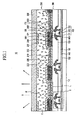
- FIG. 1 illustrates a sectional view of a display device 10, when the display device 10 is in a wide angle viewing mode
- FIG. 2 illustrates a sectional view of the display device 10, when the display device 10 is in a narrow angle viewing mode.
- the display device 10 may include a display panel 100 for displaying an image and an optical unit 300 for adjusting a viewing angle of light emitted from the display panel 100.
- the display panel 100 may be used in OLED panels, liquid crystal display (LCD) panels or plasma display panels (PDPs).
- the display panel 100 may include a plurality of pixels.
- the pixels are the basic units for displaying images and may be arranged in a matrix.
- each of the pixels may include an OLED L that emits light to display the images and a semiconductor device, e.g., a thin film transistor T, for driving the OLED L.
- the display panel 100 may include a buffer layer 120 formed on a substrate 110, and the thin film transistor T may be formed on the buffer layer 120. Further, a gate insulating layer 140 may be formed on the buffer layer 120, an interlayer dielectric layer 160 may be formed on the gate insulation layer 140 and a planarization layer 180 may be formed on the interlayer dielectric layer 160.
- the thin film transistor T may include a semiconductor layer 130, a gate electrode 150, a source electrode 171 and a drain electrode 172, formed on the buffer layer 120.
- the semiconductor layer 130 may include a source region 131, a drain region 133 and a channel region 132 interconnecting the source and drain regions 131 and 133.
- the gate insulating layer 140 may be formed on the buffer layer 120 while covering the semiconductor layer 130.
- the gate electrode 150 may be formed on the semiconductor layer 130 with the gate insulating layer 140 interposed therebetween.
- the interlayer dielectric layer 160 may be formed on the gate insulation layer 140 while covering the gate electrode 150.
- first and second contact holes 1401 and 1601 may respectively be formed in the gate insulation layer 140 and the interlayer dielectric layer 160, so that the source and drain regions 131 and 133 may be exposed through the first and second contact holes 1401 and 1601.
- the source and drain electrodes 171 and 172 may be electrically connected to the exposed source and drain regions 131 and 133, respectively.
- the substrate 110 may be formed of a metallic material, e.g., stainless steel (SUS) material, or an insulation material, e.g., glass or plastic.
- the buffer layer 120 may prevent and/or reduce impurities of the substrate 110 from diffusing into the semiconductor layer 130 when the semiconductor layer 130 is formed.
- the buffer layer 120 may be formed of a silicon nitride (SiN) layer or a multi-layer including a silicon nitride (SiN) layer and a silicon oxide (SiO 2 ) layer, for example.
- the gate electrode 150 may be a metal layer formed of at least one of molybdenum-tungsten (MoW) alloy, aluminum (Al), chromium (Cr) and aluminum/chromium-alloy (Al/Cr-alloy).
- the source electrode 171 and the drain electrode 172 may be formed of a titanium/aluminum-alloy (Ti/Al-alloy) or a titanium/aluminum/titanium-alloy Ti/Al/Ti-alloy. Other materials may be employed besides the one mentioned above.
- the planarization layer 180 may be formed on the interlayer dielectric layer 160 while covering the thin film transistor T.
- a first pixel electrode 210, an organic light emitting layer 220 and a second pixel electrode 230 may be sequentially formed on the planarization layer 180 to form the OLED L.
- the first pixel electrode 210 may be electrically connected to the drain electrode 172 of the thin film transistor T through a hole 1801 formed in the planarization layer 180.
- the first pixel electrode 210 may be electrically separated from an adjacent pixel by a pixel defining layer 240 and may contact the organic light emitting layer 220 through an opening 2401 formed in the pixel defining layer 240.
- the second pixel electrode 230 may be formed on a surface of the substrate 110 so that a voltage (e.g., a negative voltage) can be applied to the pixels arranged on the substrate 110.
- the first pixel electrode 210 may function to Inject holes and the second pixel electrode 230 may function to inject electrons.
- the first pixel electrode 210 may be a first transparent electrode formed of, for example, but not limited to, an indium tin oxide (ITO) or an indium zinc oxide (IZO). Further, the first pixel electrode 210 may be formed with a conductive reflection layer (not shown) and a second transparent electrode on the first transparent electrode (not shown) to affect a light emitting direction of the OLED L.
- the conductive reflection layer may improve electric conductivity while enhancing luminous efficiency by reflecting the light emitted from the organic light emitting layer 220.
- the conductive reflection layer may be formed of aluminum (Al), an aluminum-alloy (Al-alloy), silver (Ag), a silver-alloy (Ag-alloy), gold (Au), a gold-alloy (Au-alloy) or other combination of suitable materials.
- the second transparent electrode may suppress and/or reduce oxidation of the conductive reflection layer and may improve performance (for example a work function) between the organic light emitting layer 220 and the conductive reflection layer. Similar to the first transparent electrode, the second transparent electrode may be formed of similar materials, e.g., ITO or IZO.
- the organic light emitting layer 220 may include a light emitting layer (not shown) and organic layers (not shown).
- the light emitting layer may be the element that emits light.
- the organic layers may be respectively formed on opposite surfaces of the light emitting layer to transfer carriers, e.g., holes and electrons, to the light emitting layer.
- the organic layer may include at least one of a hole injection layer and a transport layer formed between the first pixel electrode 210 and the light emitting layer, and at least one of an electron injection layer and a transport layer formed between the light emitting layer and the second pixel electrode 230.
- the second pixel electrode 230 may be a transparent conductive layer so as to emit light in the directions as shown by arrows in FIGS. 1 and 2 .
- the transparent conductive layer may be formed of a material, e.g., ITO, IZO or an alloy made of magnesium and silver (MgAg).
- the thin film transistors T and the OLEDs L, formed on the substrate 110, may be enclosed by sealing the display panel 100 with a sealing substrate 200 creating a space S.
- the space S may be defined as a region between the display panel 100 and the sealing substrate 200.
- the optical unit 300 may be formed in the space S.
- the optical unit 300 may be formed between the second pixel electrode 230 and the sealing plate 200 without using a separate substrate.
- the optical unit 300 may further be provided on the display panel 100 to enable adjustment of the viewing angle by adjusting the light emitted from the display panel 100.
- the optical unit 300 may include a liquid crystal layer 310 and a plurality of sub-electrodes 320.
- the liquid crystal layer 310 may be formed by filling the space S with liquid crystal molecules M.
- the sub-electrodes 320 may be formed on a surface, e.g., an inner surface, of the sealing substrate 200.
- the sub-electrodes 320 may be spaced apart from each other by a predetermined distance and may be placed in regions of the display device 10 that are non-light emitting, e.g., a region where no OLED L is disposed. Accordingly, because the sub-electrodes 320 do not interfere with light emitting regions excited by the light emitted from the OLED L, a deterioration of the luminous efficiency may be prevented and/or reduced.
- the rub-electrodes 320 may be arranged in a configuration other than the one illustrated in FIGS. 1 and 2 , as long as the sub-electrodes 320 do not block/interfere with light from the OLED L.
- the sub-electrodes 320 may be formed of a transparent or a semi-transparent conductive material, e.g., ITO, IZO or MgAg alloy.
- a transparent or a semi-transparent conductive material e.g., ITO, IZO or MgAg alloy.
- the transmittance of light may be adjusted by adjusting a thickness thereof.
- the liquid crystal layer 310 may then be driven by the electric field, e.g., the liquid crystal layer 310 may transmit (or intercept) the light at each unit pixel in accordance with the electric field formed between the second pixel electrode 230 and the sub-electrodes 320. Accordingly, the electric field may selectively control the arrangement of the liquid crystal molecules M in the liquid crystal layer 310 to provide different viewing angles, e.g., a wide angle viewing mode or a narrow angle viewing mode.
- the voltage may be applied to the second pixel electrode 230 and the sub-electrodes 320 by selectively turning on the second pixel electrode 230 and the sub-electrodes 320 so that the liquid crystal molecules M may be in an "open" state, e.g., the liquid crystal molecules M may not be oriented in a substantially identical direction so that the light emitted from the display panel 100 may pass through the liquid crystal layer 310. In other words, the liquid crystal molecules M may be randomly oriented in the liquid crystal layer 310.
- This configuration provides the wide angle viewing mode and, thus, the image may be displayed as illustrated in arrow directions in FIG. 1 .
- the second pixel electrode 230 and the sub-electrodes 320 are selectively turned off and no voltage is applied to the second pixel electrode 230 and the sub-electrodes 320.
- the liquid crystal molecules M are in a "closed" state, e.g., the liquid crystal molecules M are oriented in a substantially identical direction so that light emitted from the display panel 100 is intercepted at a region where the liquid crystal molecules M are aligned/oriented in a substantially identical direction.
- the liquid crystal molecules M may be substantially uniformly oriented in the liquid crystal layer 310.
- This configuration provides the narrow angle viewing mode and in this mode the image may be displayed as illustrated in arrow directions in FIG.
- the orientation of the liquid crystal molecules M may be controlled in an opposite manner to the above, e.g., so that the liquid crystal molecules M in the open state may be in a substantially identical direction and the liquid crystal molecules M in the closed state may be in a random direction.
- the viewing angle of the display device 10 may be selectively limited.
- the optical unit 300 may be formed by utilizing the substrate 110 and the second pixel electrode 230 and the sub-electrodes 320, instead of utilizing a separate substrate, no additional panel may be required for adjusting the viewing angle. As a result, the thickness of the display device 10 may be reduced. Further, because an orientation of a liquid crystal layer 310 may be controlled using internal electrodes of the display panel 10, the manufacturing process of the display device 10 may be simplified.
- first and second etc. may be used herein to describe various elements, regions, or layers, and should not be limited by these terms. These terms are only used to distinguish an elements, region, or layer from another elements, regions, or layers. Thus, a first element, region, or layer discussed herein could be termed a second element, region, or layer without departing from the teachings of example embodiments.
- spatially relative terms such as “formed on,” “lower,” “below,” “upper,” “above,” “between,” “opposite,” “correspond” and the like, may be used herein for ease of description to describe one element or feature relationship to another element(s) or feature(s) as illustrated in the figures. It will be understood that the spatially relative terms are intended to encompass different orientations of the device in use or operation in addition to the orientation depicted in the figures. For example, if the device in the figures is turned over (or upside down), elements or layers described as “below” other elements or layers would then be oriented “above” the other elements or layers. Thus, the example term “below” can encompass both an orientation of above and below. The device may be otherwise oriented (rotated 90 degrees or at other orientations) and the spatially relative descriptors used herein interpreted accordingly.
Landscapes
- Physics & Mathematics (AREA)
- Nonlinear Science (AREA)
- Engineering & Computer Science (AREA)
- Microelectronics & Electronic Packaging (AREA)
- Chemical & Material Sciences (AREA)
- Crystallography & Structural Chemistry (AREA)
- General Physics & Mathematics (AREA)
- Optics & Photonics (AREA)
- Electroluminescent Light Sources (AREA)
- Devices For Indicating Variable Information By Combining Individual Elements (AREA)
- Liquid Crystal (AREA)
Abstract
Description
- Example embodiments relate to a display device and, more particularly, to a display device for selectively limiting a viewing angle.
- Organic light emitting diode (OLED) displays are becoming widely used due to their small size, light-weight and energy efficiency characteristics. Accordingly, OLED displays are being applied to small, portable electronic devices, e.g., cellular phones, personal digital assistant devices and portable multimedia players. Since OLED displays may be incorporated into electronic devices that are generally carried by users, images displayed on the electronic devices may be observed at various viewing angles. In other words, images on the electronic devices may be observed at a non-direct line of sight. This may yield unauthorized or unwanted observers from viewing the images on the electronic devices.
- One approach to limit the viewing angle has been to provide a polarizing plate or a polarizing film on an upper substrate of the display device. Such a polarizing plate or film, however, generally relates to a fixed viewing angle and does not allow user control of the viewing angle.
- Example embodiments are therefore directed to a display device that substantially overcome one or more of the problems due to the limitations and disadvantages of the related art.
- It is therefore a feature of example embodiments to provide a display device having an OLED display for selectively limiting a viewing angle while maintaining high performance.
- Another feature of example embodiments provides user control and selection over the viewing angle.
- Another feature of example embodiments provides a display device that may be relatively thin.
- According to an aspect of the invention there is provided a display device as set out in claim 1.
- A display device having first and second substrates arranged opposite to each other, a semiconductor device on the first substrate, a light emitting element on the first substrate, and an optical unit between the light emitting element and the second substrate is provided. The light emitting element is preferably an organic light emitting element.
- The optical unit may include a liquid crystal layer and at least one sub-electrode on the second substrate.
- The at least one sub-electrode is preferably in a non-light emitting region of the display device e.g. located on the second substrate in a location opposite to a location of the first substrate that does not comprise a light emitting element. The light emitting element may be in a light emitting region of the display device. The at least one sub-electrode may be transparent or semi-transparent and may be made using at least one of an indium tin oxide (ITO), an indium zinc oxide (IZO) and a magnesium-silver (MgAg) alloy.
- The organic light emitting element may include a first pixel electrode, an organic light emitting layer and a second pixel electrode in a stacked configuration. The first pixel electrode, the organic light emitting layer, and the second pixel electrode may be electrically connected to the semiconductor device on the first substrate. The second pixel electrode and the at least one sub-electrode may be configured to drive the liquid crystal layer. The liquid crystal layer may be between the second pixel layer and the second substrate. The organic light emitting layer may be between the first pixel electrode and the second pixel electrode. The first pixel electrode may include a reflection layer. The first pixel electrode may be made using at least one of aluminum (AI), an aluminum-alloy (Al-alloy), silver (Ag), a silver-alloy (Ag-alloy), gold (Au) and a gold-alloy (Au-alloy). The second pixel electrode may be transparent. The second pixel electrode may be made using at least one of an indium tin oxide (ITO), an indium zinc oxide (IZO) and a magnesium-silver (MgAg) alloy.
- The optical unit may be configured to randomly arrange liquid crystal molecules when a voltage is applied to the second pixel electrode and the at least one sub-electrode. The optical unit may be configured to substantially identically arrange the liquid crystal molecules when no voltage is applied to the second pixel electrode and the at least one sub-electrode.
- The display device is preferably arranged so that when a voltage difference is applied between the sub-electrode and the second pixel electrode an electric field is generated in the liquid crystal layer. This electric field preferably causes the liquid crystal molecules in the liquid crystal layer to become randomly aligned, thereby permitting light emitted from the organic light emitting element to be emitted from the display device with a wide opening angle. The liquid crystal layer is preferably arranged so that if no electric field is applied between the sub-electrode and the second pixel electrode, the liquid crystal molecules between a sub-electrode and an opposite second pixel electrode are substantially aligned with each other so that light emitted from the organic light emitting element is blocked in areas of the liquid crystal layer between sub-electrodes and the second pixel electrode by the aligned liquid crystal molecules so that light emitted from the display device is emitted with an opening angle that is smaller than the opening angle achieved when the liquid crystal molecules are not aligned.
- In an alternative embodiment the liquid crystal layer is such that the liquid crystal molecules between the sub-electrode and the second pixel electrode substantially align when an electric field of predetermined strength is created between the sub-electrode and the second pixel electrode, thereby limiting the opening angle of the light emitted from the display device, and such that the liquid crystal molecules are randomly aligned when the strength of an electric field between the sub-electrodes and the second pixel electrode is below a predetermined value or zero, thereby permitting light emission from the display device at a larger opening angle.
- The semiconductor device may be a thin film transistor. The organic light emitting element may be an OLED. The display device may be a portable display device.
- The above and other features and advantages of example embodiments will become more apparent to those of ordinary skill in the art by describing in detail example embodiments thereof with reference to the attached drawings, in which:
-
FIG. 1 illustrates a sectional view of a display device according to an example embodiment, when the display device is in a wide angle viewing mode; and -
FIG. 2 illustrates a sectional view of the display device according to another example embodiment, when the display device is in a narrow angle viewing mode. - Example embodiments will now be described more fully hereinafter with reference to the accompanying drawings; however, example embodiments may be embodied in different forms and should not be construed as limited to the embodiments set forth herein. Rather, these example embodiments are provided so that this disclosure will be thorough and complete, and will fully convey the scope of the invention to those skilled in the art.
-
FIG. 1 illustrates a sectional view of adisplay device 10, when thedisplay device 10 is in a wide angle viewing mode; andFIG. 2 illustrates a sectional view of thedisplay device 10, when thedisplay device 10 is in a narrow angle viewing mode. - Referring to
FIG. 1 , thedisplay device 10 may include adisplay panel 100 for displaying an image and anoptical unit 300 for adjusting a viewing angle of light emitted from thedisplay panel 100. Thedisplay panel 100 may be used in OLED panels, liquid crystal display (LCD) panels or plasma display panels (PDPs). - The
display panel 100 may include a plurality of pixels. The pixels are the basic units for displaying images and may be arranged in a matrix. For example, when thedisplay panel 100 is an OLED panel, each of the pixels may include an OLED L that emits light to display the images and a semiconductor device, e.g., a thin film transistor T, for driving the OLED L. - The
display panel 100 may include abuffer layer 120 formed on asubstrate 110, and the thin film transistor T may be formed on thebuffer layer 120. Further, agate insulating layer 140 may be formed on thebuffer layer 120, an interlayerdielectric layer 160 may be formed on thegate insulation layer 140 and aplanarization layer 180 may be formed on the interlayerdielectric layer 160. - The thin film transistor T may include a
semiconductor layer 130, agate electrode 150, asource electrode 171 and adrain electrode 172, formed on thebuffer layer 120. Thesemiconductor layer 130 may include asource region 131, adrain region 133 and achannel region 132 interconnecting the source anddrain regions - The
gate insulating layer 140 may be formed on thebuffer layer 120 while covering thesemiconductor layer 130. Thegate electrode 150 may be formed on thesemiconductor layer 130 with thegate insulating layer 140 interposed therebetween. - The interlayer
dielectric layer 160 may be formed on thegate insulation layer 140 while covering thegate electrode 150. In an example embodiment, first andsecond contact holes gate insulation layer 140 and the interlayerdielectric layer 160, so that the source anddrain regions second contact holes drain electrodes drain regions - The
substrate 110 may be formed of a metallic material, e.g., stainless steel (SUS) material, or an insulation material, e.g., glass or plastic. Thebuffer layer 120 may prevent and/or reduce impurities of thesubstrate 110 from diffusing into thesemiconductor layer 130 when thesemiconductor layer 130 is formed. Thebuffer layer 120 may be formed of a silicon nitride (SiN) layer or a multi-layer including a silicon nitride (SiN) layer and a silicon oxide (SiO2) layer, for example. Thegate electrode 150 may be a metal layer formed of at least one of molybdenum-tungsten (MoW) alloy, aluminum (Al), chromium (Cr) and aluminum/chromium-alloy (Al/Cr-alloy). Thesource electrode 171 and thedrain electrode 172 may be formed of a titanium/aluminum-alloy (Ti/Al-alloy) or a titanium/aluminum/titanium-alloy Ti/Al/Ti-alloy. Other materials may be employed besides the one mentioned above. - The
planarization layer 180 may be formed on theinterlayer dielectric layer 160 while covering the thin film transistor T. Afirst pixel electrode 210, an organiclight emitting layer 220 and asecond pixel electrode 230 may be sequentially formed on theplanarization layer 180 to form the OLED L. - The
first pixel electrode 210 may be electrically connected to thedrain electrode 172 of the thin film transistor T through ahole 1801 formed in theplanarization layer 180. Thefirst pixel electrode 210 may be electrically separated from an adjacent pixel by apixel defining layer 240 and may contact the organiclight emitting layer 220 through anopening 2401 formed in thepixel defining layer 240. - The
second pixel electrode 230 may be formed on a surface of thesubstrate 110 so that a voltage (e.g., a negative voltage) can be applied to the pixels arranged on thesubstrate 110. Thefirst pixel electrode 210 may function to Inject holes and thesecond pixel electrode 230 may function to inject electrons. - The
first pixel electrode 210 may be a first transparent electrode formed of, for example, but not limited to, an indium tin oxide (ITO) or an indium zinc oxide (IZO). Further, thefirst pixel electrode 210 may be formed with a conductive reflection layer (not shown) and a second transparent electrode on the first transparent electrode (not shown) to affect a light emitting direction of the OLED L. The conductive reflection layer may improve electric conductivity while enhancing luminous efficiency by reflecting the light emitted from the organiclight emitting layer 220. The conductive reflection layer may be formed of aluminum (Al), an aluminum-alloy (Al-alloy), silver (Ag), a silver-alloy (Ag-alloy), gold (Au), a gold-alloy (Au-alloy) or other combination of suitable materials. The second transparent electrode may suppress and/or reduce oxidation of the conductive reflection layer and may improve performance (for example a work function) between the organiclight emitting layer 220 and the conductive reflection layer. Similar to the first transparent electrode, the second transparent electrode may be formed of similar materials, e.g., ITO or IZO. - The organic
light emitting layer 220 may include a light emitting layer (not shown) and organic layers (not shown). The light emitting layer may be the element that emits light. The organic layers may be respectively formed on opposite surfaces of the light emitting layer to transfer carriers, e.g., holes and electrons, to the light emitting layer. For example, the organic layer may include at least one of a hole injection layer and a transport layer formed between thefirst pixel electrode 210 and the light emitting layer, and at least one of an electron injection layer and a transport layer formed between the light emitting layer and thesecond pixel electrode 230. - The
second pixel electrode 230 may be a transparent conductive layer so as to emit light in the directions as shown by arrows inFIGS. 1 and2 . The transparent conductive layer may be formed of a material, e.g., ITO, IZO or an alloy made of magnesium and silver (MgAg). - The thin film transistors T and the OLEDs L, formed on the
substrate 110, may be enclosed by sealing thedisplay panel 100 with a sealingsubstrate 200 creating a space S. The space S may be defined as a region between thedisplay panel 100 and the sealingsubstrate 200. Theoptical unit 300 may be formed in the space S. In detail, theoptical unit 300 may be formed between thesecond pixel electrode 230 and the sealingplate 200 without using a separate substrate. Theoptical unit 300 may further be provided on thedisplay panel 100 to enable adjustment of the viewing angle by adjusting the light emitted from thedisplay panel 100. - The
optical unit 300 may include aliquid crystal layer 310 and a plurality ofsub-electrodes 320. Theliquid crystal layer 310 may be formed by filling the space S with liquid crystal molecules M. The sub-electrodes 320 may be formed on a surface, e.g., an inner surface, of the sealingsubstrate 200. - The sub-electrodes 320 may be spaced apart from each other by a predetermined distance and may be placed in regions of the
display device 10 that are non-light emitting, e.g., a region where no OLED L is disposed. Accordingly, because the sub-electrodes 320 do not interfere with light emitting regions excited by the light emitted from the OLED L, a deterioration of the luminous efficiency may be prevented and/or reduced. The rub-electrodes 320 may be arranged in a configuration other than the one illustrated inFIGS. 1 and2 , as long as the sub-electrodes 320 do not block/interfere with light from the OLED L. The sub-electrodes 320 may be formed of a transparent or a semi-transparent conductive material, e.g., ITO, IZO or MgAg alloy. When the sub-electrodes 320 are formed of a MgAg alloy, the transmittance of light may be adjusted by adjusting a thickness thereof. - Now, a method of adjusting viewing angles of light emitted from the
display device 10 by selectively applying a voltage to thedisplay panel 100 will be described in detail. - In particular, when a voltage is applied to the
second pixel electrode 230, a predetermined voltage may be applied to thesub-electrodes 320 to form an electric field between thesecond pixel electrode 230 and the sub-electrodes 320. Theliquid crystal layer 310 may then be driven by the electric field, e.g., theliquid crystal layer 310 may transmit (or intercept) the light at each unit pixel in accordance with the electric field formed between thesecond pixel electrode 230 and the sub-electrodes 320. Accordingly, the electric field may selectively control the arrangement of the liquid crystal molecules M in theliquid crystal layer 310 to provide different viewing angles, e.g., a wide angle viewing mode or a narrow angle viewing mode. - In the wide angle viewing mode (as illustrated in
FIG. 1 ), the voltage may be applied to thesecond pixel electrode 230 and thesub-electrodes 320 by selectively turning on thesecond pixel electrode 230 and thesub-electrodes 320 so that the liquid crystal molecules M may be in an "open" state, e.g., the liquid crystal molecules M may not be oriented in a substantially identical direction so that the light emitted from thedisplay panel 100 may pass through theliquid crystal layer 310. In other words, the liquid crystal molecules M may be randomly oriented in theliquid crystal layer 310. This configuration provides the wide angle viewing mode and, thus, the image may be displayed as illustrated in arrow directions inFIG. 1 . - In the narrow angle viewing mode (as illustrated in
FIG. 2 ), thesecond pixel electrode 230 and thesub-electrodes 320 are selectively turned off and no voltage is applied to thesecond pixel electrode 230 and the sub-electrodes 320. In this configuration the liquid crystal molecules M are in a "closed" state, e.g., the liquid crystal molecules M are oriented in a substantially identical direction so that light emitted from thedisplay panel 100 is intercepted at a region where the liquid crystal molecules M are aligned/oriented in a substantially identical direction. In other words, the liquid crystal molecules M may be substantially uniformly oriented in theliquid crystal layer 310. This configuration provides the narrow angle viewing mode and in this mode the image may be displayed as illustrated in arrow directions inFIG. 2 . It will of course be appreciated that the orientation of the liquid crystal molecules M may be controlled in an opposite manner to the above, e.g., so that the liquid crystal molecules M in the open state may be in a substantially identical direction and the liquid crystal molecules M in the closed state may be in a random direction. - As a result, by turning on or off the
second pixel electrode 230 and thesub-electrodes 320, the viewing angle of thedisplay device 10 may be selectively limited. - As in the preferred embodiment the
optical unit 300 may be formed by utilizing thesubstrate 110 and thesecond pixel electrode 230 and thesub-electrodes 320, instead of utilizing a separate substrate, no additional panel may be required for adjusting the viewing angle. As a result, the thickness of thedisplay device 10 may be reduced. Further, because an orientation of aliquid crystal layer 310 may be controlled using internal electrodes of thedisplay panel 10, the manufacturing process of thedisplay device 10 may be simplified. - In the figures, the thickness of layers, panels, regions, substrates, etc., are exaggerated for clarity. It will be understood that when an element such as a layer, a a panel, a region, or a substrate is referred to as being "on" another element, it can be directly on the other element or intervening elements may also be present. In contrast, when an element or layer is referred to as being "directly on," "directly connected to" or "directly coupled to" another element or layer, there are no intervening elements or layers present. Further, it will be understood that when a layer, film, region, or substrate is referred to as being "under" or "above" another layer, it can be directly under or directly above, and one or more intervening layers, films, panels, regions, substrates may also be present. In addition, it will also be understood that when a layer is referred to as being "between" two layers, it can be the only layer between the two layers, or one or more intervening layers may also be present. Further, when it is described that a unit "includes" a constituent element, it means that the unit may further include other constituent elements in addition to the element unless specifically referred to the contrary. Like numbers refer to like elements throughout. As used herein, the term "and/or" includes any and all combinations of one or more of the associated listed items.
- It will also be understood that, although the terms "first" and "second" etc. may be used herein to describe various elements, regions, or layers, and should not be limited by these terms. These terms are only used to distinguish an elements, region, or layer from another elements, regions, or layers. Thus, a first element, region, or layer discussed herein could be termed a second element, region, or layer without departing from the teachings of example embodiments.
- Spatially relative terms, such as "formed on," "lower," "below," "upper," "above," "between," "opposite," "correspond" and the like, may be used herein for ease of description to describe one element or feature relationship to another element(s) or feature(s) as illustrated in the figures. It will be understood that the spatially relative terms are intended to encompass different orientations of the device in use or operation in addition to the orientation depicted in the figures. For example, if the device in the figures is turned over (or upside down), elements or layers described as "below" other elements or layers would then be oriented "above" the other elements or layers. Thus, the example term "below" can encompass both an orientation of above and below. The device may be otherwise oriented (rotated 90 degrees or at other orientations) and the spatially relative descriptors used herein interpreted accordingly.
- Example embodiments have been disclosed herein, and although specific terms are employed, they are used and are to be interpreted in a generic and descriptive sense only and not for purpose of limitation. Accordingly, it will be understood by those of ordinary skill in the art that various changes in form and details may be made without departing from the scope of the present invention as set forth in the following claims.
Claims (18)
- A display device, comprising:first and second substrates arranged opposite to each other,a semiconductor device on the first substrate;a light emitting element on the first substrate; andan optical unit between the light emitting element and the second substrate.
- The display device as claimed in claim 1, wherein the optical unit comprises:a liquid crystal layer, andat least one sub-electrode on the second substrate.
- The display device as claimed in claim 2, wherein the at least one sub-electrode is in a non-light emitting region of the display device.
- The display device as claimed in claim 3, wherein the light emitting element is in a light emitting region of the display device.
- The display device as claimed in claim 2, 3 or 4, wherein the at least one sub-electrode is transparent or semi-transparent.
- The display device as claimed in claim 4, wherein the at least one sub-electrode is made using at least one of an indium tin oxide (ITO), an indium zinc oxide (IZO) and a magnesium-silver (MgAg) alloy.
- The display device as claimed in any of claims 2 to 6,, wherein:the light emitting element is an organic light emitting element that includes a first pixel electrode, an organic light emitting layer, and a second pixel electrode in a stacked configuration, the first pixel electrode, the organic light emitting layer, and the second pixel electrode are configured to be electrically connected to the semiconductor device on the first substrate; andthe second pixel electrode and the at least one sub-electrode are configured to drive the liquid crystal layer.
- The display device as claimed in claim 7, wherein the liquid crystal layer is between the second pixel electrode and the second substrate.
- The display device as claimed in claim 7 or 8, wherein the organic light emitting layer is between the first pixel electrode and the second pixel electrode.
- The display device as claimed in claim 7,8 or 9 wherein the first pixel electrode includes a reflection layer.
- The display device as claimed in claim 10, wherein the first pixel electrode is made using at least one of aluminum, an aluminum-alloy, silver, a silver-alloy, gold and a gold-alloy.
- The display device as claimed in claim 7,8 or 9, wherein the second pixel electrode is transparent.
- The display device as claimed in claim 12, wherein the second pixel electrode is made using at least one of an indium tin oxide, an indium zinc oxide and a magnesium-silver alloy.
- The display device as claimed in any of claims 7 to 13, wherein the optical unit is configured to randomly arrange liquid crystal molecules when a voltage is applied to the second pixel electrode and the at least one sub-electrode.
- The display device as claimed in claim 14, wherein the optical unit is configured to substantially identically arrange the liquid crystal molecules when no voltage is applied to the second pixel electrode and the at least one sub-electrode.
- The display device as claimed in any preceding claim, wherein the semiconductor device is a thin film transistor.
- The display device as claimed in any preceding claim, wherein the organic light emitting element is an organic light emitting diode.
- The display device as claimed in any preceding claim, wherein the display device is a portable display device.
Applications Claiming Priority (1)
| Application Number | Priority Date | Filing Date | Title |
|---|---|---|---|
| KR1020070077727A KR100869810B1 (en) | 2007-08-02 | 2007-08-02 | Display device |
Publications (2)
| Publication Number | Publication Date |
|---|---|
| EP2023396A1 true EP2023396A1 (en) | 2009-02-11 |
| EP2023396B1 EP2023396B1 (en) | 2017-01-11 |
Family
ID=39885049
Family Applications (1)
| Application Number | Title | Priority Date | Filing Date |
|---|---|---|---|
| EP08252383.8A Ceased EP2023396B1 (en) | 2007-08-02 | 2008-07-11 | Display device |
Country Status (5)
| Country | Link |
|---|---|
| US (1) | US8344969B2 (en) |
| EP (1) | EP2023396B1 (en) |
| JP (1) | JP4964731B2 (en) |
| KR (1) | KR100869810B1 (en) |
| CN (1) | CN101359113B (en) |
Cited By (1)
| Publication number | Priority date | Publication date | Assignee | Title |
|---|---|---|---|---|
| CN103325956A (en) * | 2012-03-23 | 2013-09-25 | 株式会社东芝 | Organic electroluminescent device, lighting apparatus, and method for manufacturing the organic electroluminescent device |
Families Citing this family (20)
| Publication number | Priority date | Publication date | Assignee | Title |
|---|---|---|---|---|
| US8026531B2 (en) * | 2005-03-22 | 2011-09-27 | Semiconductor Energy Laboratory Co., Ltd. | Light emitting device |
| KR101741167B1 (en) | 2010-10-22 | 2017-05-30 | 삼성디스플레이 주식회사 | Organic light emitting diode display |
| KR101784994B1 (en) * | 2011-03-31 | 2017-10-13 | 삼성디스플레이 주식회사 | Organic light emitting diode display and manufacturing method thereof |
| KR20140041119A (en) * | 2012-09-27 | 2014-04-04 | 삼성디스플레이 주식회사 | Organic light emitting display device |
| KR102096622B1 (en) * | 2013-08-19 | 2020-04-03 | 삼성디스플레이 주식회사 | Organic light emitting display device |
| KR102105061B1 (en) * | 2014-01-06 | 2020-04-28 | 삼성디스플레이 주식회사 | Organic light emitting diode2 display panel and manufacturing method of the same |
| US9710013B2 (en) * | 2014-08-08 | 2017-07-18 | Semiconductor Energy Laboratory Co., Ltd. | Display panel, data processing device, program |
| CN104503115B (en) | 2015-01-14 | 2017-12-05 | 合肥鑫晟光电科技有限公司 | A kind of display panel and display device |
| WO2017072634A1 (en) * | 2015-10-30 | 2017-05-04 | Semiconductor Energy Laboratory Co., Ltd. | Display device, electronic device, and method for manufacturing display device and electronic device |
| US11107372B2 (en) | 2016-03-31 | 2021-08-31 | Sony Corporation | Display device and electronic apparatus |
| TWI603135B (en) * | 2016-10-13 | 2017-10-21 | 財團法人工業技術研究院 | Three dimensional display module |
| CN109686761B (en) * | 2018-12-14 | 2020-10-02 | 云谷(固安)科技有限公司 | display panel |
| KR102248969B1 (en) * | 2020-03-27 | 2021-05-10 | 삼성디스플레이 주식회사 | Organic light emitting display device |
| US11862113B2 (en) * | 2020-08-13 | 2024-01-02 | Chongqing Konka Photoelectric Technology Research Institute Co., Ltd. | Display panel and electronic device |
| WO2022039010A1 (en) * | 2020-08-18 | 2022-02-24 | 京セラ株式会社 | Display device |
| KR102926527B1 (en) * | 2020-12-18 | 2026-02-11 | 엘지디스플레이 주식회사 | Display apparatus realizing a narrow viewing angle |
| KR102823813B1 (en) * | 2020-12-24 | 2025-06-20 | 엘지디스플레이 주식회사 | Organic light emitting display device |
| CN112712754B (en) * | 2020-12-31 | 2022-08-19 | 联想(北京)有限公司 | Display device and electronic apparatus |
| KR102829968B1 (en) * | 2021-03-17 | 2025-07-08 | 삼성디스플레이 주식회사 | Display device and method of operating a display device |
| KR20240153489A (en) * | 2023-04-14 | 2024-10-23 | 삼성디스플레이 주식회사 | Display device |
Citations (4)
| Publication number | Priority date | Publication date | Assignee | Title |
|---|---|---|---|---|
| US20030052869A1 (en) * | 2001-09-14 | 2003-03-20 | Sharp Kabushiki Kaisha | Display, method of manufacturing the same, and method of driving the same |
| US20030201960A1 (en) | 2002-04-30 | 2003-10-30 | Nec Corporation | Display device and driving method thereof |
| EP1475655A1 (en) | 2003-05-09 | 2004-11-10 | Seiko Epson Corporation | Viewing angle control element, display device, and electronic apparatus |
| US20050035353A1 (en) * | 2003-08-13 | 2005-02-17 | Hitachi Displays, Ltd. | Light emitting display |
Family Cites Families (10)
| Publication number | Priority date | Publication date | Assignee | Title |
|---|---|---|---|---|
| JP3481741B2 (en) | 1995-09-06 | 2003-12-22 | セイコーエプソン株式会社 | Image display device |
| JP2000075287A (en) * | 1998-09-01 | 2000-03-14 | Toshiba Corp | Reflective liquid crystal display |
| JP2002140022A (en) * | 2000-11-01 | 2002-05-17 | Matsushita Electric Ind Co Ltd | Display device and method of manufacturing display device |
| US20030112397A1 (en) * | 2001-12-13 | 2003-06-19 | Hannstar Display Corporation | Biased bending vertical alignment mode liquid crystal display |
| JP4623701B2 (en) * | 2003-08-29 | 2011-02-02 | 株式会社 日立ディスプレイズ | Coloring composition for color filter and display device using color filter formed with this coloring composition |
| JP2005158369A (en) * | 2003-11-21 | 2005-06-16 | Toyota Industries Corp | Optical member and lighting device |
| JP2005190768A (en) * | 2003-12-25 | 2005-07-14 | Toyota Industries Corp | Lighting device |
| GB2413394A (en) * | 2004-04-20 | 2005-10-26 | Sharp Kk | Display |
| JP4332515B2 (en) * | 2004-04-28 | 2009-09-16 | キヤノン株式会社 | Liquid crystal display |
| CN100346220C (en) | 2004-12-07 | 2007-10-31 | 友达光电股份有限公司 | Liquid crystal display with adjustable display viewing angle and display method thereof |
-
2007
- 2007-08-02 KR KR1020070077727A patent/KR100869810B1/en active Active
- 2007-10-09 JP JP2007263546A patent/JP4964731B2/en not_active Expired - Fee Related
-
2008
- 2008-03-18 US US12/076,401 patent/US8344969B2/en active Active
- 2008-04-30 CN CN2008100944826A patent/CN101359113B/en not_active Expired - Fee Related
- 2008-07-11 EP EP08252383.8A patent/EP2023396B1/en not_active Ceased
Patent Citations (4)
| Publication number | Priority date | Publication date | Assignee | Title |
|---|---|---|---|---|
| US20030052869A1 (en) * | 2001-09-14 | 2003-03-20 | Sharp Kabushiki Kaisha | Display, method of manufacturing the same, and method of driving the same |
| US20030201960A1 (en) | 2002-04-30 | 2003-10-30 | Nec Corporation | Display device and driving method thereof |
| EP1475655A1 (en) | 2003-05-09 | 2004-11-10 | Seiko Epson Corporation | Viewing angle control element, display device, and electronic apparatus |
| US20050035353A1 (en) * | 2003-08-13 | 2005-02-17 | Hitachi Displays, Ltd. | Light emitting display |
Cited By (3)
| Publication number | Priority date | Publication date | Assignee | Title |
|---|---|---|---|---|
| CN103325956A (en) * | 2012-03-23 | 2013-09-25 | 株式会社东芝 | Organic electroluminescent device, lighting apparatus, and method for manufacturing the organic electroluminescent device |
| EP2642522A1 (en) * | 2012-03-23 | 2013-09-25 | Kabushiki Kaisha Toshiba | Organic electroluminescent device, lighting apparatus, and method for manufacturing the organic electroluminescent device |
| US8902383B2 (en) | 2012-03-23 | 2014-12-02 | Kabushiki Kaisha Toshiba | Organic electroluminescent device, lighting apparatus, and method for manufacturing the organic electroluminescent device |
Also Published As
| Publication number | Publication date |
|---|---|
| EP2023396B1 (en) | 2017-01-11 |
| US8344969B2 (en) | 2013-01-01 |
| KR100869810B1 (en) | 2008-11-21 |
| US20090033596A1 (en) | 2009-02-05 |
| CN101359113B (en) | 2010-06-02 |
| CN101359113A (en) | 2009-02-04 |
| JP4964731B2 (en) | 2012-07-04 |
| JP2009038332A (en) | 2009-02-19 |
Similar Documents
| Publication | Publication Date | Title |
|---|---|---|
| EP2023396B1 (en) | Display device | |
| CN102759834B (en) | Display device and the method operating this display device | |
| CN102856347B (en) | For controlling the display device of light transmission | |
| EP2216840B1 (en) | Organic light emitting diode display | |
| US8237354B2 (en) | Organic light emitting diode display | |
| US9548339B2 (en) | Organic light emitting diode display device | |
| EP2618378B1 (en) | Organic light emitting display device | |
| US8736790B2 (en) | Organic light emitting diode display with liquid crystal layer | |
| US8797239B2 (en) | Organic light-emitting display device | |
| CN110676299A (en) | Organic Light Emitting Display Device | |
| JP2003249370A (en) | Active matrix organic light emitting display and method of manufacturing the same | |
| US8426861B2 (en) | Organic light emitting display device | |
| US20110037683A1 (en) | Organic light emitting diode display | |
| CN100473248C (en) | Organic light-emitting device and manufacturing method thereof | |
| KR20160006520A (en) | Organic light emitting display device and method of fabricating the same | |
| KR20160010165A (en) | Organic light emitting display device and method of fabricating the same | |
| US20160351854A1 (en) | Organic light emitting diode display device | |
| EP2197061B1 (en) | Organic light emitting diode display | |
| US7535172B2 (en) | Organic light emitting diode display | |
| US12048217B2 (en) | Display device | |
| US12238972B2 (en) | Display device | |
| US20070194318A1 (en) | Organic light emitting diode display |
Legal Events
| Date | Code | Title | Description |
|---|---|---|---|
| PUAI | Public reference made under article 153(3) epc to a published international application that has entered the european phase |
Free format text: ORIGINAL CODE: 0009012 |
|
| 17P | Request for examination filed |
Effective date: 20080716 |
|
| AK | Designated contracting states |
Kind code of ref document: A1 Designated state(s): AT BE BG CH CY CZ DE DK EE ES FI FR GB GR HR HU IE IS IT LI LT LU LV MC MT NL NO PL PT RO SE SI SK TR |
|
| AX | Request for extension of the european patent |
Extension state: AL BA MK RS |
|
| RAP1 | Party data changed (applicant data changed or rights of an application transferred) |
Owner name: SAMSUNG MOBILE DISPLAY CO., LTD. |
|
| AKX | Designation fees paid |
Designated state(s): DE FR GB |
|
| 17Q | First examination report despatched |
Effective date: 20110211 |
|
| RAP1 | Party data changed (applicant data changed or rights of an application transferred) |
Owner name: SAMSUNG DISPLAY CO., LTD. |
|
| RAP1 | Party data changed (applicant data changed or rights of an application transferred) |
Owner name: SAMSUNG DISPLAY CO., LTD. |
|
| GRAP | Despatch of communication of intention to grant a patent |
Free format text: ORIGINAL CODE: EPIDOSNIGR1 |
|
| INTG | Intention to grant announced |
Effective date: 20160722 |
|
| GRAS | Grant fee paid |
Free format text: ORIGINAL CODE: EPIDOSNIGR3 |
|
| GRAA | (expected) grant |
Free format text: ORIGINAL CODE: 0009210 |
|
| AK | Designated contracting states |
Kind code of ref document: B1 Designated state(s): DE FR GB |
|
| REG | Reference to a national code |
Ref country code: GB Ref legal event code: FG4D |
|
| REG | Reference to a national code |
Ref country code: DE Ref legal event code: R096 Ref document number: 602008048329 Country of ref document: DE |
|
| REG | Reference to a national code |
Ref country code: FR Ref legal event code: PLFP Year of fee payment: 10 |
|
| REG | Reference to a national code |
Ref country code: DE Ref legal event code: R097 Ref document number: 602008048329 Country of ref document: DE |
|
| PLBE | No opposition filed within time limit |
Free format text: ORIGINAL CODE: 0009261 |
|
| STAA | Information on the status of an ep patent application or granted ep patent |
Free format text: STATUS: NO OPPOSITION FILED WITHIN TIME LIMIT |
|
| 26N | No opposition filed |
Effective date: 20171012 |
|
| REG | Reference to a national code |
Ref country code: FR Ref legal event code: PLFP Year of fee payment: 11 |
|
| REG | Reference to a national code |
Ref country code: DE Ref legal event code: R079 Ref document number: 602008048329 Country of ref document: DE Free format text: PREVIOUS MAIN CLASS: H01L0027320000 Ipc: H10K0059000000 |
|
| P01 | Opt-out of the competence of the unified patent court (upc) registered |
Effective date: 20230515 |
|
| PGFP | Annual fee paid to national office [announced via postgrant information from national office to epo] |
Ref country code: GB Payment date: 20240620 Year of fee payment: 17 |
|
| PGFP | Annual fee paid to national office [announced via postgrant information from national office to epo] |
Ref country code: FR Payment date: 20240624 Year of fee payment: 17 |
|
| PGFP | Annual fee paid to national office [announced via postgrant information from national office to epo] |
Ref country code: DE Payment date: 20240620 Year of fee payment: 17 |
|
| REG | Reference to a national code |
Ref country code: DE Ref legal event code: R119 Ref document number: 602008048329 Country of ref document: DE |
|
| GBPC | Gb: european patent ceased through non-payment of renewal fee |
Effective date: 20250711 |
|
| PG25 | Lapsed in a contracting state [announced via postgrant information from national office to epo] |
Ref country code: GB Free format text: LAPSE BECAUSE OF NON-PAYMENT OF DUE FEES Effective date: 20250711 |
|
| PG25 | Lapsed in a contracting state [announced via postgrant information from national office to epo] |
Ref country code: DE Free format text: LAPSE BECAUSE OF NON-PAYMENT OF DUE FEES Effective date: 20260203 |
|
| PG25 | Lapsed in a contracting state [announced via postgrant information from national office to epo] |
Ref country code: FR Free format text: LAPSE BECAUSE OF NON-PAYMENT OF DUE FEES Effective date: 20250731 |