EP2023381A1 - Method of selectively forming atomically flat plane on diamond surface, diamond substrate produced by the method, and semiconductor element employing the same - Google Patents
Method of selectively forming atomically flat plane on diamond surface, diamond substrate produced by the method, and semiconductor element employing the same Download PDFInfo
- Publication number
- EP2023381A1 EP2023381A1 EP07742189A EP07742189A EP2023381A1 EP 2023381 A1 EP2023381 A1 EP 2023381A1 EP 07742189 A EP07742189 A EP 07742189A EP 07742189 A EP07742189 A EP 07742189A EP 2023381 A1 EP2023381 A1 EP 2023381A1
- Authority
- EP
- European Patent Office
- Prior art keywords
- diamond
- semiconductor layer
- conductivity type
- inclined surface
- misorientation angle
- Prior art date
- Legal status (The legal status is an assumption and is not a legal conclusion. Google has not performed a legal analysis and makes no representation as to the accuracy of the status listed.)
- Withdrawn
Links
Images




Classifications
-
- C—CHEMISTRY; METALLURGY
- C23—COATING METALLIC MATERIAL; COATING MATERIAL WITH METALLIC MATERIAL; CHEMICAL SURFACE TREATMENT; DIFFUSION TREATMENT OF METALLIC MATERIAL; COATING BY VACUUM EVAPORATION, BY SPUTTERING, BY ION IMPLANTATION OR BY CHEMICAL VAPOUR DEPOSITION, IN GENERAL; INHIBITING CORROSION OF METALLIC MATERIAL OR INCRUSTATION IN GENERAL
- C23C—COATING METALLIC MATERIAL; COATING MATERIAL WITH METALLIC MATERIAL; SURFACE TREATMENT OF METALLIC MATERIAL BY DIFFUSION INTO THE SURFACE, BY CHEMICAL CONVERSION OR SUBSTITUTION; COATING BY VACUUM EVAPORATION, BY SPUTTERING, BY ION IMPLANTATION OR BY CHEMICAL VAPOUR DEPOSITION, IN GENERAL
- C23C16/00—Chemical coating by decomposition of gaseous compounds, without leaving reaction products of surface material in the coating, i.e. chemical vapour deposition [CVD] processes
- C23C16/22—Chemical coating by decomposition of gaseous compounds, without leaving reaction products of surface material in the coating, i.e. chemical vapour deposition [CVD] processes characterised by the deposition of inorganic material, other than metallic material
- C23C16/26—Deposition of carbon only
- C23C16/27—Diamond only
- C23C16/279—Diamond only control of diamond crystallography
-
- C—CHEMISTRY; METALLURGY
- C23—COATING METALLIC MATERIAL; COATING MATERIAL WITH METALLIC MATERIAL; CHEMICAL SURFACE TREATMENT; DIFFUSION TREATMENT OF METALLIC MATERIAL; COATING BY VACUUM EVAPORATION, BY SPUTTERING, BY ION IMPLANTATION OR BY CHEMICAL VAPOUR DEPOSITION, IN GENERAL; INHIBITING CORROSION OF METALLIC MATERIAL OR INCRUSTATION IN GENERAL
- C23C—COATING METALLIC MATERIAL; COATING MATERIAL WITH METALLIC MATERIAL; SURFACE TREATMENT OF METALLIC MATERIAL BY DIFFUSION INTO THE SURFACE, BY CHEMICAL CONVERSION OR SUBSTITUTION; COATING BY VACUUM EVAPORATION, BY SPUTTERING, BY ION IMPLANTATION OR BY CHEMICAL VAPOUR DEPOSITION, IN GENERAL
- C23C16/00—Chemical coating by decomposition of gaseous compounds, without leaving reaction products of surface material in the coating, i.e. chemical vapour deposition [CVD] processes
- C23C16/22—Chemical coating by decomposition of gaseous compounds, without leaving reaction products of surface material in the coating, i.e. chemical vapour deposition [CVD] processes characterised by the deposition of inorganic material, other than metallic material
- C23C16/26—Deposition of carbon only
- C23C16/27—Diamond only
-
- C—CHEMISTRY; METALLURGY
- C30—CRYSTAL GROWTH
- C30B—SINGLE-CRYSTAL GROWTH; UNIDIRECTIONAL SOLIDIFICATION OF EUTECTIC MATERIAL OR UNIDIRECTIONAL DEMIXING OF EUTECTOID MATERIAL; REFINING BY ZONE-MELTING OF MATERIAL; PRODUCTION OF A HOMOGENEOUS POLYCRYSTALLINE MATERIAL WITH DEFINED STRUCTURE; SINGLE CRYSTALS OR HOMOGENEOUS POLYCRYSTALLINE MATERIAL WITH DEFINED STRUCTURE; AFTER-TREATMENT OF SINGLE CRYSTALS OR A HOMOGENEOUS POLYCRYSTALLINE MATERIAL WITH DEFINED STRUCTURE; APPARATUS THEREFOR
- C30B25/00—Single-crystal growth by chemical reaction of reactive gases, e.g. chemical vapour-deposition growth
- C30B25/02—Epitaxial-layer growth
- C30B25/18—Epitaxial-layer growth characterised by the substrate
- C30B25/20—Epitaxial-layer growth characterised by the substrate the substrate being of the same materials as the epitaxial layer
- C30B25/205—Epitaxial-layer growth characterised by the substrate the substrate being of the same materials as the epitaxial layer the substrate being of insulating material
-
- C—CHEMISTRY; METALLURGY
- C30—CRYSTAL GROWTH
- C30B—SINGLE-CRYSTAL GROWTH; UNIDIRECTIONAL SOLIDIFICATION OF EUTECTIC MATERIAL OR UNIDIRECTIONAL DEMIXING OF EUTECTOID MATERIAL; REFINING BY ZONE-MELTING OF MATERIAL; PRODUCTION OF A HOMOGENEOUS POLYCRYSTALLINE MATERIAL WITH DEFINED STRUCTURE; SINGLE CRYSTALS OR HOMOGENEOUS POLYCRYSTALLINE MATERIAL WITH DEFINED STRUCTURE; AFTER-TREATMENT OF SINGLE CRYSTALS OR A HOMOGENEOUS POLYCRYSTALLINE MATERIAL WITH DEFINED STRUCTURE; APPARATUS THEREFOR
- C30B29/00—Single crystals or homogeneous polycrystalline material with defined structure characterised by the material or by their shape
- C30B29/02—Elements
- C30B29/04—Diamond
-
- H—ELECTRICITY
- H10—SEMICONDUCTOR DEVICES; ELECTRIC SOLID-STATE DEVICES NOT OTHERWISE PROVIDED FOR
- H10P—GENERIC PROCESSES OR APPARATUS FOR THE MANUFACTURE OR TREATMENT OF DEVICES COVERED BY CLASS H10
- H10P14/00—Formation of materials, e.g. in the shape of layers or pillars
- H10P14/20—Formation of materials, e.g. in the shape of layers or pillars of semiconductor materials
-
- H—ELECTRICITY
- H10—SEMICONDUCTOR DEVICES; ELECTRIC SOLID-STATE DEVICES NOT OTHERWISE PROVIDED FOR
- H10P—GENERIC PROCESSES OR APPARATUS FOR THE MANUFACTURE OR TREATMENT OF DEVICES COVERED BY CLASS H10
- H10P14/00—Formation of materials, e.g. in the shape of layers or pillars
- H10P14/20—Formation of materials, e.g. in the shape of layers or pillars of semiconductor materials
- H10P14/24—Formation of materials, e.g. in the shape of layers or pillars of semiconductor materials using chemical vapour deposition [CVD]
-
- H—ELECTRICITY
- H10—SEMICONDUCTOR DEVICES; ELECTRIC SOLID-STATE DEVICES NOT OTHERWISE PROVIDED FOR
- H10P—GENERIC PROCESSES OR APPARATUS FOR THE MANUFACTURE OR TREATMENT OF DEVICES COVERED BY CLASS H10
- H10P14/00—Formation of materials, e.g. in the shape of layers or pillars
- H10P14/20—Formation of materials, e.g. in the shape of layers or pillars of semiconductor materials
- H10P14/29—Formation of materials, e.g. in the shape of layers or pillars of semiconductor materials characterised by the substrates
- H10P14/2901—Materials
- H10P14/2902—Materials being Group IVA materials
- H10P14/2903—Carbon, e.g. diamond-like carbon
-
- H—ELECTRICITY
- H10—SEMICONDUCTOR DEVICES; ELECTRIC SOLID-STATE DEVICES NOT OTHERWISE PROVIDED FOR
- H10P—GENERIC PROCESSES OR APPARATUS FOR THE MANUFACTURE OR TREATMENT OF DEVICES COVERED BY CLASS H10
- H10P14/00—Formation of materials, e.g. in the shape of layers or pillars
- H10P14/20—Formation of materials, e.g. in the shape of layers or pillars of semiconductor materials
- H10P14/29—Formation of materials, e.g. in the shape of layers or pillars of semiconductor materials characterised by the substrates
- H10P14/2926—Crystal orientations
-
- H—ELECTRICITY
- H10—SEMICONDUCTOR DEVICES; ELECTRIC SOLID-STATE DEVICES NOT OTHERWISE PROVIDED FOR
- H10P—GENERIC PROCESSES OR APPARATUS FOR THE MANUFACTURE OR TREATMENT OF DEVICES COVERED BY CLASS H10
- H10P14/00—Formation of materials, e.g. in the shape of layers or pillars
- H10P14/20—Formation of materials, e.g. in the shape of layers or pillars of semiconductor materials
- H10P14/34—Deposited materials, e.g. layers
- H10P14/3402—Deposited materials, e.g. layers characterised by the chemical composition
- H10P14/3404—Deposited materials, e.g. layers characterised by the chemical composition being Group IVA materials
- H10P14/3406—Carbon, e.g. diamond-like carbon
-
- H—ELECTRICITY
- H10—SEMICONDUCTOR DEVICES; ELECTRIC SOLID-STATE DEVICES NOT OTHERWISE PROVIDED FOR
- H10P—GENERIC PROCESSES OR APPARATUS FOR THE MANUFACTURE OR TREATMENT OF DEVICES COVERED BY CLASS H10
- H10P14/00—Formation of materials, e.g. in the shape of layers or pillars
- H10P14/20—Formation of materials, e.g. in the shape of layers or pillars of semiconductor materials
- H10P14/34—Deposited materials, e.g. layers
- H10P14/3438—Doping during depositing
- H10P14/3441—Conductivity type
- H10P14/3442—N-type
-
- H—ELECTRICITY
- H10—SEMICONDUCTOR DEVICES; ELECTRIC SOLID-STATE DEVICES NOT OTHERWISE PROVIDED FOR
- H10P—GENERIC PROCESSES OR APPARATUS FOR THE MANUFACTURE OR TREATMENT OF DEVICES COVERED BY CLASS H10
- H10P14/00—Formation of materials, e.g. in the shape of layers or pillars
- H10P14/20—Formation of materials, e.g. in the shape of layers or pillars of semiconductor materials
- H10P14/34—Deposited materials, e.g. layers
- H10P14/3438—Doping during depositing
- H10P14/3441—Conductivity type
- H10P14/3444—P-type
-
- H—ELECTRICITY
- H10—SEMICONDUCTOR DEVICES; ELECTRIC SOLID-STATE DEVICES NOT OTHERWISE PROVIDED FOR
- H10P—GENERIC PROCESSES OR APPARATUS FOR THE MANUFACTURE OR TREATMENT OF DEVICES COVERED BY CLASS H10
- H10P14/00—Formation of materials, e.g. in the shape of layers or pillars
- H10P14/20—Formation of materials, e.g. in the shape of layers or pillars of semiconductor materials
- H10P14/27—Formation of materials, e.g. in the shape of layers or pillars of semiconductor materials using selective deposition, e.g. simultaneous growth of monocrystalline and non-monocrystalline semiconductor materials
Definitions
- the present invention relates to epitaxial growth of diamond, and, more particularly, to epitaxial growth of diamond which can improve semiconductor device performance and a method of selectively forming a flat plane on an atomic level on a diamond surface.
- Non-patent Document 1 There is a report on the formation of a step-terrace structure on a diamond (001) substrate at a methane concentration of 0.025% using microwave plasma CVD (see Non-patent Document 1).
- Non-patent Document 2 it is known that a mesa surface is formed atomically flat by carrying out chemical vapor deposition (H 2 (4400 cm 3 /min), SiH 4 (2.7 cm 3 /min), C 3 H 8 (0.3 cm 3 /min), 1600°C, 20 mbar for 30 minutes) after forming a mesa structure on SiC substrate (see Non-patent Document 2).
- Non-patent Document 3 It is also known that a mesa surface is formed flat by carrying out deposition at a substrate temperature of 850°C with a supersonic beam Si 2 H 6 as a source material after forming a mesa structure on Si (111) substrate (see Non-patent Document 3).
- Non-patent Document 4 a mesa surface, is made atomically flat by carrying out metalorganic vapor phase epitaxy after forming a mesa structure on a GaAs (111) B substrate using SiO 2 mask.
- Non-patent Document 1 H. Watanabe, D. Takeuchi, S. Yamanaka, H. Okushi, K. Kajimura, T. Sekiguchi, Diamond and Related Materials 8 (1999) 1272-1276 .
- Non-patent Document 2 J. Anthony Powell, Philip G. Neudeck, Andrew J. Trunek, Glenn M. Beheim, Lawrence G. Matus, Richard W. Hoffman, Jr., and Luann J. Key, Growth of step-free surfaces on device-size (0001) SiC mesas, Applied Physics Letters Vol. 77 (2000) 1449-1451 .
- Non-patent Document 3 Doohan Lee, Jack M. Blakely, Todd W. Schroeder and J. R. Engstrom, A growth method for creating arrays of atomically flat mesas on silicon, Applied Physics Letters Vol. 78 (2001) 1349-1351 .
- Non-patent Document 4 Toshio Nishida and Naoki Kobayashi, Step-free surface grown on GaAs (111) B substrate by selective area metalorganic vapor phase epitaxy, Applied Physics Letters Vol. 69 (1996) 2549-2550 .
- step-flow growth was employed after forming a mesa structure on the (001), (110) or (111) surface of diamond using the method to attempt selective formation of a flat plane on the mesa surface, it was found that a flat plane could be also selectively formed on the (001), (110) or (111) surface of diamond, and further, selective formation of a complete step-free diamond surface was realized.
- the present invention provides a method of selectively forming a plane flat on the atomic level on the (001), (110) or (111) surface of diamond.
- the present invention is a method of selectively forming an atomically flat plane on a diamond surface comprising growing diamond on a stepped diamond surface of any of crystal structures (001), (110) and (111) by CVD (Chemical Vapor Deposition) under growth conditions such that step-flow growth of diamond is carried out thereafter.
- CVD Chemical Vapor Deposition
- the stepped diamond surface should be acquired by depositing a metal on a surface of a diamond substrate with any one of the crystal structures (001), (110) and (111), processing the metal using a lithography technique, and then etching the diamond using the metal as a mask.
- microwave plasma CVD may be used as CVD.
- a feed amount of a carbon source gas can be controlled such that the feed amount of the carbon source gas is 0.001% to 0.2% in the step-flow growth.
- an atomically flat plane could be selectively formed on the (001), (110) or (111) surface of diamond, and that a complete step-free diamond surface could be selectively formed.
- a diamond surface to be used in the present invention has a crystal structure (001), (110) or (111), and the present invention can also be implemented even on a surface with a crystal structure (110) though its embodiment is not illustrated.
- a mask to be used in the invention is typically gold, platinum or the like, a metal oxide, such as alumina, or silicon oxide can be used instead.
- Lithographies are well-known means in the industry, and a well-known lithography can be employed.
- the process comprises application of a resist, exposure and development.
- Typical lithographies include a photolithography using light and an electronic lithography using electrons, at the time of exposure. Any resist can be used in the present invention as long as it is cured by exposure.
- a typical one is ZEP520A or the like.
- Typical etching is dry etching using ICP (Inductively Coupled Plasma).
- Step-flow growth according to the present invention is a method which allows a step to be grown by priority, and needs to control growth conditions, such as the concentration of a carbon source gas, according to the type (001), (110) or (111) of the diamond surface to be used.
- carbon source gas to be used in the present invention a mixture of carbon hydride, such as methane or ethane, carbon oxide, carbon dioxide and hydrogen is used. At this time, oxygen or a rare gas may be mixed.
- CVD Chemical Vapor Deposition
- microwave plasma CVD is desirable.
- a resist film was formed on the surface of a diamond substrate (001), desired locations of the resist were removed by electron beam exposure, and then gold was evaporated so that a layer of gold was provided on the diamond substrate (001) surface. Next, lift-off was performed to form a gold layer only at the resist-removed portions. Then, the diamond substrate was processed by diamond etching, and a step (mesa structure) was provided by removing the gold layer, after which diamond was grown under growth conditions (1200 W, 50 Torr, hydrogen concentration of 99.95%, methane concentration of 0.05%) for the step-flow growth of diamond by using microwave plasma CVD.
- a diamond substrate provided with a step (mesa structure) was prepared, diamond was epitaxially grown by CVD, and it was confirmed that the surface of the step became atomically flat by the epitaxial growth mechanism.
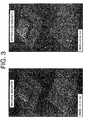
- Fig. 3 shows the results.
- Example 2 The same manipulation as that of the Example 1 was performed except for the use of a diamond (111) substrate. It is to be noted that the hydrogen concentration was 99.995% and the methane concentration was 0.005%.
- Figs. 4 and 5 show the results.
- a wider surface ( Fig. 5 ) on the mesa has an atomically flat plane and a plane including an atomic step, and a portion having a surface shape similar to that of growth on the substrate. It indicates that the formation of an atomically flat plane is in a midway.
- An Ib diamond (111) substrate obtained by high temperature/high pressure conductivity type composition was introduced into a reactor of a microwave plasma CVD apparatus, and a p + diamond film having a low resistance was grown.
- the boron concentration in the film was 10 20 atoms/cm 3 .
- the substrate was removed from the reactor and a step (mesa structure) was provided on the surface of the diamond film using a lithography technique.
- a p-type diamond film was grown under growth conditions for step-flow growth of diamond.
- the boron concentration in the film was 10 17 atoms/cm 3 .
- an n-type diamond film was formed by step-flow growth having nucleation of diamond.
- the phosphorus concentration in the film was 10 17 atoms/cm 3 .
- the pn junction on the mesa had an atomically flat interface.
- the diamond film other than the mesa structure was selectively etched until the low-resistance diamond film formed first appeared, an electrode with a low contact resistance was formed on the low-resistance diamond film and the n-type diamond surface on the mesa structure, thereby forming a pn-junction semiconductor device.
- An exemplary diagram of the cross-sectional structure is shown in Fig. 6 .
- a pn-junction semiconductor device in which a high-quality i layer having few impurity is provided at the pn junction interface can also be prepared.
- An exemplary diagram of the cross-sectional structure is shown in Fig. 7 .
- an n + layer (phosphorus concentration of 10 19 to 10 22 atoms/cm 3 in the film) may be provided at the metal-n-type diamond film interface to reduce the contact resistance.
- step control and doping control on the nano level can be expected.
Landscapes
- Chemical & Material Sciences (AREA)
- Engineering & Computer Science (AREA)
- Materials Engineering (AREA)
- Metallurgy (AREA)
- Organic Chemistry (AREA)
- Crystallography & Structural Chemistry (AREA)
- General Chemical & Material Sciences (AREA)
- Chemical Kinetics & Catalysis (AREA)
- Inorganic Chemistry (AREA)
- Mechanical Engineering (AREA)
- Crystals, And After-Treatments Of Crystals (AREA)
- Chemical Vapour Deposition (AREA)
Abstract
Description
- The present invention relates to epitaxial growth of diamond, and, more particularly, to epitaxial growth of diamond which can improve semiconductor device performance and a method of selectively forming a flat plane on an atomic level on a diamond surface.
- There has been known that a homoepitaxially grown film surface of diamond is likely to have defects, such as abnormally grown particles, macrobunching, and etch pits, formed thereon.
- Those defects deteriorate the device performance. With regard to other materials, the planarization of the surface in the device performance is very important, and those defects need to be suppressed in a device to be prepared in device fabrication using diamond.
- There is a report on the formation of a step-terrace structure on a diamond (001) substrate at a methane concentration of 0.025% using microwave plasma CVD (see Non-patent Document 1).
- However, such a flat surface cannot be obtained on a (111) substrate. The device fabrication using diamond, therefore, needs a technique of selectively forming a flat surface of the device size.
- Meanwhile, with regard to other materials, it is known that a mesa surface is formed atomically flat by carrying out chemical vapor deposition (H2(4400 cm3/min), SiH4(2.7 cm3/min), C3H8(0.3 cm3/min), 1600°C, 20 mbar for 30 minutes) after forming a mesa structure on SiC substrate (see Non-patent Document 2).
- It is also known that a mesa surface is formed flat by carrying out deposition at a substrate temperature of 850°C with a supersonic beam Si2H6 as a source material after forming a mesa structure on Si (111) substrate (see Non-patent Document 3).
- Further, it is known that a mesa surface, is made atomically flat by carrying out metalorganic vapor phase epitaxy after forming a mesa structure on a GaAs (111) B substrate using SiO2 mask (see Non-patent Document 4).
- Non-patent Document 1: H. Watanabe, D. Takeuchi, S. Yamanaka, H. Okushi, K. Kajimura, T. Sekiguchi, Diamond and Related Materials 8 (1999) 1272-1276.
- Non-patent Document 2: J. Anthony Powell, Philip G. Neudeck, Andrew J. Trunek, Glenn M. Beheim, Lawrence G. Matus, Richard W. Hoffman, Jr., and Luann J. Key, Growth of step-free surfaces on device-size (0001) SiC mesas, Applied Physics Letters Vol. 77 (2000) 1449-1451.
- Non-patent Document 3: Doohan Lee, Jack M. Blakely, Todd W. Schroeder and J. R. Engstrom, A growth method for creating arrays of atomically flat mesas on silicon, Applied Physics Letters Vol. 78 (2001) 1349-1351.
- Non-patent Document 4: Toshio Nishida and Naoki Kobayashi, Step-free surface grown on GaAs (111) B substrate by selective area metalorganic vapor phase epitaxy, Applied Physics Letters Vol. 69 (1996) 2549-2550.
- According to the present invention, step-flow growth was employed after forming a mesa structure on the (001), (110) or (111) surface of diamond using the method to attempt selective formation of a flat plane on the mesa surface, it was found that a flat plane could be also selectively formed on the (001), (110) or (111) surface of diamond, and further, selective formation of a complete step-free diamond surface was realized. The present invention provides a method of selectively forming a plane flat on the atomic level on the (001), (110) or (111) surface of diamond.
- The present invention is a method of selectively forming an atomically flat plane on a diamond surface comprising growing diamond on a stepped diamond surface of any of crystal structures (001), (110) and (111) by CVD (Chemical Vapor Deposition) under growth conditions such that step-flow growth of diamond is carried out thereafter.
- According to the present invention, it is desirable that the stepped diamond surface should be acquired by depositing a metal on a surface of a diamond substrate with any one of the crystal structures (001), (110) and (111), processing the metal using a lithography technique, and then etching the diamond using the metal as a mask.
- Further, according to the present invention, microwave plasma CVD may be used as CVD.
- Furthermore, according to the present invention, a feed amount of a carbon source gas can be controlled such that the feed amount of the carbon source gas is 0.001% to 0.2% in the step-flow growth.
- According to the present invention, it was found that an atomically flat plane could be selectively formed on the (001), (110) or (111) surface of diamond, and that a complete step-free diamond surface could be selectively formed.
-
-
Fig. 1 is an exemplary diagram of the concept (atomically flat plane) of the present invention; -
Fig. 2 shows an example of the process of the present invention; -
Fig. 3 shows an AFM image of the (001) surface of diamond; -
Fig. 4 shows an AFM image of the (111) surface of diamond; -
Fig. 5 shows an AFM image of the (111) surface of diamond; -
Fig. 6 shows an example of a semiconductor device using a diamond substrate acquired by the method of the present invention; and -
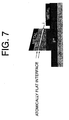
Fig. 7 shows an example of a semiconductor device using a diamond substrate acquired by the method of the present invention. - A diamond surface to be used in the present invention has a crystal structure (001), (110) or (111), and the present invention can also be implemented even on a surface with a crystal structure (110) though its embodiment is not illustrated.
- While a mask to be used in the invention is typically gold, platinum or the like, a metal oxide, such as alumina, or silicon oxide can be used instead.
- Lithographies are well-known means in the industry, and a well-known lithography can be employed. The process comprises application of a resist, exposure and development. Typical lithographies include a photolithography using light and an electronic lithography using electrons, at the time of exposure. Any resist can be used in the present invention as long as it is cured by exposure. A typical one is ZEP520A or the like.
- Well-known popular diamond etching can be used to etch diamond to be used in the present invention. Typical etching is dry etching using ICP (Inductively Coupled Plasma).
- While a typical example of a diamond surface with a step (mesa structure) according to the present invention is obtained through steps as shown in
Fig. 2 , selective formation of an atomically flat plane according to the invention can be carried out as long as a diamond surface has a step (mesa structure). - Step-flow growth according to the present invention is a method which allows a step to be grown by priority, and needs to control growth conditions, such as the concentration of a carbon source gas, according to the type (001), (110) or (111) of the diamond surface to be used.
- As the carbon source gas to be used in the present invention, a mixture of carbon hydride, such as methane or ethane, carbon oxide, carbon dioxide and hydrogen is used. At this time, oxygen or a rare gas may be mixed.
- CVD (Chemical Vapor Deposition) can be used as means for the step-flow growth according to the present invention.
- Particularly, the use of microwave plasma CVD is desirable.
- Although the present invention will be described in more details by way of examples, the present invention is not limited to those examples.
- A description will be given based on a process in
Fig. 2 . - A resist film was formed on the surface of a diamond substrate (001), desired locations of the resist were removed by electron beam exposure, and then gold was evaporated so that a layer of gold was provided on the diamond substrate (001) surface. Next, lift-off was performed to form a gold layer only at the resist-removed portions. Then, the diamond substrate was processed by diamond etching, and a step (mesa structure) was provided by removing the gold layer, after which diamond was grown under growth conditions (1200 W, 50 Torr, hydrogen concentration of 99.95%, methane concentration of 0.05%) for the step-flow growth of diamond by using microwave plasma CVD.
- This is illustrated in an exemplary diagram in
Fig. 1 . - That is, a diamond substrate provided with a step (mesa structure) was prepared, diamond was epitaxially grown by CVD, and it was confirmed that the surface of the step became atomically flat by the epitaxial growth mechanism.
-
Fig. 3 shows the results. - The same manipulation as that of the Example 1 was performed except for the use of a diamond (111) substrate. It is to be noted that the hydrogen concentration was 99.995% and the methane concentration was 0.005%.
-
Figs. 4 and5 show the results. - A wider surface (
Fig. 5 ) on the mesa has an atomically flat plane and a plane including an atomic step, and a portion having a surface shape similar to that of growth on the substrate. It indicates that the formation of an atomically flat plane is in a midway. - An Ib diamond (111) substrate obtained by high temperature/high pressure conductivity type composition was introduced into a reactor of a microwave plasma CVD apparatus, and a p+ diamond film having a low resistance was grown. The boron concentration in the film was 1020 atoms/cm3. Thereafter, the substrate was removed from the reactor and a step (mesa structure) was provided on the surface of the diamond film using a lithography technique. Then, it was placed in the reactor of the microwave plasma CVD apparatus, and a p-type diamond film was grown under growth conditions for step-flow growth of diamond. The boron concentration in the film was 1017 atoms/cm3. Thereafter, an n-type diamond film was formed by step-flow growth having nucleation of diamond. The phosphorus concentration in the film was 1017 atoms/cm3. The pn junction on the mesa had an atomically flat interface. The diamond film other than the mesa structure was selectively etched until the low-resistance diamond film formed first appeared, an electrode with a low contact resistance was formed on the low-resistance diamond film and the n-type diamond surface on the mesa structure, thereby forming a pn-junction semiconductor device. An exemplary diagram of the cross-sectional structure is shown in
Fig. 6 . - A pn-junction semiconductor device in which a high-quality i layer having few impurity is provided at the pn junction interface can also be prepared. An exemplary diagram of the cross-sectional structure is shown in
Fig. 7 . - In the semiconductor device, an n+ layer (phosphorus concentration of 1019 to 1022 atoms/cm3 in the film) may be provided at the metal-n-type diamond film interface to reduce the contact resistance.
- According to the present invention, not only selective formation of an atomically flat plane on a diamond surface but also step control and doping control on the nano level, such as delta doping, can be expected.
Claims (9)
- A method of selectively forming a flat plane on a diamond surface comprising growing diamond on a stepped diamond surface of any of crystal structures (001), (110) and (111) by CVD (Chemical Vapor Deposition) under growth conditions such that step-flow growth of diamond is carried out thereafter.
- The method of selectively forming a flat plane on a diamond surface according to claim 1, wherein a metal is disposed on the stepped surface of a diamond substrate of any of (001), (110) and (111) or diamond film homoepitaxially grown by CVD, patterning the metal in an intended pattern, and etching the diamond, and then removing the metal.
- The method of selectively forming an atomically flat plane on a diamond surface according to claim 1, wherein CVD is microwave plasma CVD.
- The method of selectively forming a flat plane on a diamond surface according to any one of claims 1 to 3, wherein in the step-flow growth, a feed amount of a carbon source gas is 0.001% to 0.2%.
- A diamond substrate having a main diamond surface of any of crystal structures (001), (110) and (111), the main surface having a plane substantially flat on an atomic level which has a predetermined misorientation angle to the surface and selectively grown along an inclined surface of the misorientation angle from a top of the misorientation angle.
- The diamond substrate according to claim 5, wherein the substrate has a mesa structure.
- A semiconductor device comprising:a diamond substrate;a semiconductor layer of a first conductivity type deposited by growing diamond on the substrate, the semiconductor layer having an inclined surface formed to have a predetermined misorientation angle to a surface thereof and be selectively grown along the inclined surface of the misorientation angle from a top of the misorientation angle;a semiconductor layer of a second conductivity type deposited by growing diamond on the inclined surface of the semiconductor layer of the first conductivity type, an interface between the inclined surface of the semiconductor layer of the first conductivity type and the semiconductor layer of the second conductivity type forming a plane substantially flat on an atomic level; anda metal electrode deposited on the semiconductor layer of the second conductivity type.
- A semiconductor device comprising:a diamond substrate;a semiconductor layer of a first conductivity type deposited by growing diamond on the substrate, the semiconductor layer having an inclined surface formed to have a predetermined misorientation angle to a surface thereof and be selectively grown along the inclined surface of the misorientation angle from a top of the misorientation angle;an intrinsic semiconductor layer deposited by growing diamond on the inclined surface of the semiconductor layer of the first conductivity type;a semiconductor layer of a second conductivity type deposited by growing diamond on the inclined surface of the semiconductor layer of the first conductivity type, an interface between the inclined surface of the semiconductor layer of the first conductivity type and the semiconductor layer of the second conductivity type forming a plane substantially flat on an atomic level; anda metal electrode deposited on the semiconductor layer of the second conductivity type.
- An electronic device comprising:a semiconductor layer of a first conductivity type having an inclined surface formed to have a predetermined misorientation angle to a surface thereof and be selectively grown along the inclined surface of the misorientation angle from a top of the misorientation angle;a semiconductor layer of a second conductivity type deposited by growing diamond on the inclined surface of the semiconductor layer of the first conductivity type, an interface between the inclined surface of the semiconductor layer of the first conductivity type and the semiconductor layer of the second conductivity type forming a plane substantially flat on an atomic level; anda metal electrode deposited on the semiconductor layer of the second conductivity type.
Applications Claiming Priority (2)
| Application Number | Priority Date | Filing Date | Title |
|---|---|---|---|
| JP2006132145 | 2006-05-11 | ||
| PCT/JP2007/058754 WO2007132644A1 (en) | 2006-05-11 | 2007-04-23 | Method of selectively forming atomically flat plane on diamond surface, diamond substrate produced by the method, and semiconductor element employing the same |
Publications (2)
| Publication Number | Publication Date |
|---|---|
| EP2023381A1 true EP2023381A1 (en) | 2009-02-11 |
| EP2023381A4 EP2023381A4 (en) | 2011-11-09 |
Family
ID=38693743
Family Applications (1)
| Application Number | Title | Priority Date | Filing Date |
|---|---|---|---|
| EP07742189A Withdrawn EP2023381A4 (en) | 2006-05-11 | 2007-04-23 | PROCESS FOR SELECTIVELY FORMING AN ATOMIC FLAT PLAN AT A DIAMOND SURFACE, DIAMOND SUBSTRATE OBTAINED THEREFROM, AND SEMICONDUCTOR ELEMENT EMPLOYING IT |
Country Status (4)
| Country | Link |
|---|---|
| US (1) | US7989260B2 (en) |
| EP (1) | EP2023381A4 (en) |
| JP (1) | JP4446065B2 (en) |
| WO (1) | WO2007132644A1 (en) |
Families Citing this family (7)
| Publication number | Priority date | Publication date | Assignee | Title |
|---|---|---|---|---|
| JP5028879B2 (en) * | 2006-06-27 | 2012-09-19 | 住友電気工業株式会社 | Method for producing diamond single crystal with thin film and diamond single crystal with thin film |
| JP5071815B2 (en) * | 2008-08-29 | 2012-11-14 | 独立行政法人産業技術総合研究所 | Calibration standard of scanning microscope using nanometer scale measurement standard sample and nanometer scale measurement standard sample |
| JP5454867B2 (en) * | 2009-04-17 | 2014-03-26 | 独立行政法人産業技術総合研究所 | Single crystal diamond substrate |
| US9469918B2 (en) * | 2014-01-24 | 2016-10-18 | Ii-Vi Incorporated | Substrate including a diamond layer and a composite layer of diamond and silicon carbide, and, optionally, silicon |
| US9922823B1 (en) * | 2016-09-07 | 2018-03-20 | Euclid Techlabs, Llc | CVD reactor and method for nanometric delta doping of diamond |
| WO2024196396A1 (en) * | 2023-03-20 | 2024-09-26 | M7D Corporation | Defect reduction in diamond |
| NL2038407B1 (en) * | 2024-08-07 | 2026-02-23 | Univ Delft Tech | Method of manufacturing a diamond substrate |
Family Cites Families (2)
| Publication number | Priority date | Publication date | Assignee | Title |
|---|---|---|---|---|
| JP2763172B2 (en) * | 1990-03-19 | 1998-06-11 | 株式会社神戸製鋼所 | Diamond thin film etching method |
| WO2003106743A1 (en) * | 2002-06-01 | 2003-12-24 | 住友電気工業株式会社 | N-type semiconductor diamond producing method and semiconductor diamond |
-
2007
- 2007-04-23 WO PCT/JP2007/058754 patent/WO2007132644A1/en not_active Ceased
- 2007-04-23 JP JP2008515473A patent/JP4446065B2/en not_active Expired - Fee Related
- 2007-04-23 US US12/227,163 patent/US7989260B2/en not_active Expired - Fee Related
- 2007-04-23 EP EP07742189A patent/EP2023381A4/en not_active Withdrawn
Also Published As
| Publication number | Publication date |
|---|---|
| EP2023381A4 (en) | 2011-11-09 |
| WO2007132644A1 (en) | 2007-11-22 |
| US7989260B2 (en) | 2011-08-02 |
| JP4446065B2 (en) | 2010-04-07 |
| US20090127566A1 (en) | 2009-05-21 |
| JPWO2007132644A1 (en) | 2009-09-24 |
Similar Documents
| Publication | Publication Date | Title |
|---|---|---|
| JP3127342B2 (en) | Synthetic semiconductors and their controlled doping | |
| Koleske et al. | Influence of MOVPE growth conditions on carbon and silicon concentrations in GaN | |
| US5709745A (en) | Compound semi-conductors and controlled doping thereof | |
| US7989260B2 (en) | Method of selectively forming atomically flat plane on diamond surface, diamond substrate produced by the method, and semiconductor device using the same | |
| US20060211210A1 (en) | Material for selective deposition and etching | |
| TWI459589B (en) | Method for preparing epitaxial structure | |
| JP5478616B2 (en) | Method for reducing memory effect in semiconductor epitaxy | |
| US20080318359A1 (en) | Method of manufacturing silicon carbide semiconductor substrate | |
| TW201344946A (en) | Epitaxial structure | |
| KR102018449B1 (en) | Semiconductor wafer comprising a single crystal IIIA nitride layer | |
| CN101627458A (en) | Nitride semiconductor structures with interlayer structures and methods of fabricating nitride semiconductor structures with interlayer structures | |
| TW201344951A (en) | Epitaxial structure | |
| Gudovskikh et al. | Low temperature plasma enhanced deposition of GaP films on Si substrate | |
| Tokuda | Homoepitaxial diamond growth by plasma-enhanced chemical vapor deposition | |
| Gillis et al. | Highly anisotropic, ultra-smooth patterning of GaN/SiC by low energy electron enhanced etching in DC plasma | |
| WO2012029216A1 (en) | Method for manufacturing compound semiconductor | |
| US20070224784A1 (en) | Semiconductor material having an epitaxial layer formed thereon and methods of making same | |
| JP4742399B2 (en) | Method for producing group 3-5 compound semiconductor | |
| CN115074825A (en) | Silicon carbide epitaxial structure, pulse type growth method and application thereof | |
| CN112602171A (en) | Epitaxial substrate | |
| JPH07130981A (en) | Semiconductor electron-emitting device and method of forming the same | |
| Fini | Threading dislocation reduction in gallium nitride thin films on sapphire via lateral epitaxial overgrowth | |
| TW202537440A (en) | Semiconductor structure and manufacturing method thereof | |
| Fuendling et al. | GaN and ZnO nanostructures | |
| CN120299986A (en) | A method for growing single crystal diamond from silicon wafer |
Legal Events
| Date | Code | Title | Description |
|---|---|---|---|
| PUAI | Public reference made under article 153(3) epc to a published international application that has entered the european phase |
Free format text: ORIGINAL CODE: 0009012 |
|
| 17P | Request for examination filed |
Effective date: 20081127 |
|
| AK | Designated contracting states |
Kind code of ref document: A1 Designated state(s): AT BE BG CH CY CZ DE DK EE ES FI FR GB GR HU IE IS IT LI LT LU LV MC MT NL PL PT RO SE SI SK TR |
|
| AX | Request for extension of the european patent |
Extension state: AL BA HR MK RS |
|
| DAX | Request for extension of the european patent (deleted) | ||
| RBV | Designated contracting states (corrected) |
Designated state(s): DE ES FR GB IT |
|
| A4 | Supplementary search report drawn up and despatched |
Effective date: 20111007 |
|
| RIC1 | Information provided on ipc code assigned before grant |
Ipc: C30B 25/20 20060101ALI20110930BHEP Ipc: C23C 16/511 20060101ALI20110930BHEP Ipc: H01L 21/02 20060101ALI20110930BHEP Ipc: C23C 16/27 20060101ALI20110930BHEP Ipc: C30B 29/04 20060101ALI20110930BHEP Ipc: H01L 21/205 20060101AFI20110930BHEP |
|
| 17Q | First examination report despatched |
Effective date: 20120703 |
|
| STAA | Information on the status of an ep patent application or granted ep patent |
Free format text: STATUS: THE APPLICATION IS DEEMED TO BE WITHDRAWN |
|
| 18D | Application deemed to be withdrawn |
Effective date: 20161203 |