EP2023206A1 - Exposure apparatus and device manufacturing method - Google Patents
Exposure apparatus and device manufacturing method Download PDFInfo
- Publication number
- EP2023206A1 EP2023206A1 EP08162028A EP08162028A EP2023206A1 EP 2023206 A1 EP2023206 A1 EP 2023206A1 EP 08162028 A EP08162028 A EP 08162028A EP 08162028 A EP08162028 A EP 08162028A EP 2023206 A1 EP2023206 A1 EP 2023206A1
- Authority
- EP
- European Patent Office
- Prior art keywords
- movable body
- exposure apparatus
- stop
- substrate
- driver
- Prior art date
- Legal status (The legal status is an assumption and is not a legal conclusion. Google has not performed a legal analysis and makes no representation as to the accuracy of the status listed.)
- Withdrawn
Links
- 238000004519 manufacturing process Methods 0.000 title claims description 7
- 230000004044 response Effects 0.000 claims abstract description 5
- 239000000758 substrate Substances 0.000 claims description 21
- 230000003287 optical effect Effects 0.000 claims description 12
- 230000005856 abnormality Effects 0.000 claims description 2
- 230000001133 acceleration Effects 0.000 claims description 2
- 238000000034 method Methods 0.000 claims description 2
- 238000001514 detection method Methods 0.000 claims 1
- 230000007246 mechanism Effects 0.000 description 9
- 230000003213 activating effect Effects 0.000 description 6
- 238000005286 illumination Methods 0.000 description 4
- 239000004065 semiconductor Substances 0.000 description 4
- 230000004913 activation Effects 0.000 description 2
- 238000010586 diagram Methods 0.000 description 2
- 238000001459 lithography Methods 0.000 description 2
- 230000001172 regenerating effect Effects 0.000 description 2
- 230000002411 adverse Effects 0.000 description 1
- 230000001427 coherent effect Effects 0.000 description 1
- 238000005530 etching Methods 0.000 description 1
- 239000004973 liquid crystal related substance Substances 0.000 description 1
- QSHDDOUJBYECFT-UHFFFAOYSA-N mercury Chemical compound [Hg] QSHDDOUJBYECFT-UHFFFAOYSA-N 0.000 description 1
- 229910052753 mercury Inorganic materials 0.000 description 1
- 238000012986 modification Methods 0.000 description 1
- 230000004048 modification Effects 0.000 description 1
- 238000004806 packaging method and process Methods 0.000 description 1
- 230000008569 process Effects 0.000 description 1
- 238000007493 shaping process Methods 0.000 description 1
- 239000010409 thin film Substances 0.000 description 1
- 229910052724 xenon Inorganic materials 0.000 description 1
- FHNFHKCVQCLJFQ-UHFFFAOYSA-N xenon atom Chemical compound [Xe] FHNFHKCVQCLJFQ-UHFFFAOYSA-N 0.000 description 1
Images

Classifications
-
- G—PHYSICS
- G03—PHOTOGRAPHY; CINEMATOGRAPHY; ANALOGOUS TECHNIQUES USING WAVES OTHER THAN OPTICAL WAVES; ELECTROGRAPHY; HOLOGRAPHY
- G03F—PHOTOMECHANICAL PRODUCTION OF TEXTURED OR PATTERNED SURFACES, e.g. FOR PRINTING, FOR PROCESSING OF SEMICONDUCTOR DEVICES; MATERIALS THEREFOR; ORIGINALS THEREFOR; APPARATUS SPECIALLY ADAPTED THEREFOR
- G03F7/00—Photomechanical, e.g. photolithographic, production of textured or patterned surfaces, e.g. printing surfaces; Materials therefor, e.g. comprising photoresists; Apparatus specially adapted therefor
- G03F7/70—Microphotolithographic exposure; Apparatus therefor
- G03F7/70691—Handling of masks or workpieces
- G03F7/70716—Stages
- G03F7/70725—Stages control
-
- G—PHYSICS
- G03—PHOTOGRAPHY; CINEMATOGRAPHY; ANALOGOUS TECHNIQUES USING WAVES OTHER THAN OPTICAL WAVES; ELECTROGRAPHY; HOLOGRAPHY
- G03F—PHOTOMECHANICAL PRODUCTION OF TEXTURED OR PATTERNED SURFACES, e.g. FOR PRINTING, FOR PROCESSING OF SEMICONDUCTOR DEVICES; MATERIALS THEREFOR; ORIGINALS THEREFOR; APPARATUS SPECIALLY ADAPTED THEREFOR
- G03F7/00—Photomechanical, e.g. photolithographic, production of textured or patterned surfaces, e.g. printing surfaces; Materials therefor, e.g. comprising photoresists; Apparatus specially adapted therefor
- G03F7/70—Microphotolithographic exposure; Apparatus therefor
- G03F7/70691—Handling of masks or workpieces
- G03F7/70758—Drive means, e.g. actuators, motors for long- or short-stroke modules or fine or coarse driving
Definitions
- the present invention relates to an exposure apparatus and a method of manufacturing a device.
- a process of manufacturing a semiconductor device includes a lithography step of transferring by exposure a circuit pattern formed on an original onto a substrate.
- the original and substrate are fixed on an original stage and substrate stage, respectively, and these stages are driven in synchrony by linear motors, thereby performing exposure.
- an apparatus power source is disconnected as soon as a power shutdown signal is transmitted when a power shutdown switch or emergency stop switch is turned on.
- a linear motor used to drive the stage is stopped by, for example, a regenerative brake.
- Japanese Patent Laid-Open No. 2001-60614 discloses an exposure apparatus having an emergency stop switch of a two-step structure formed by a first-step switch for activating a brake mechanism, and a second-step switch for activating a power shutdown device.
- the emergency stop switch when the emergency stop switch is turned on, the power shutdown device stops power supplied from a power source to a power driving system and the brake mechanism.
- the emergency stop switch has a two-step structure formed by the first-step switch for activating the brake mechanism, and the second-step for activating the power shutdown device, so that these two switches are activated with a predetermined time lag sufficient to stop traveling of a stage.
- the brake mechanism performs brake control of the power driving system as the first-step switch is activated.
- the second-step switch is activated a predetermined time after the activation of the first-step switch so that the power shutdown device stops power supplied from the power source to the power driving system and brake mechanism. Therefore, the power supply to the power driving system is stopped after traveling of the stage is stopped.
- the linear motor may damage upon colliding against, for example, its mechanical stopper depending on the position, moving velocity, and moving direction of the stage.
- the risk of such damage is increasing.
- the exposure apparatus disclosed in Japanese Patent Laid-Open No. 2001-60614 uses a time lag of, for example, several hundreds of milliseconds between the activation of the brake mechanism and that of the power shutdown device.
- the stage may travel at high speed in activating the brake mechanism, and it may still travel at high speed even in activating the power shutdown device.
- the stage can be urgently decelerated within a predetermined time lag by changing the brake condition of the brake mechanism.
- the urgent deceleration may impose a heavy load on the stage, resulting in its deformation.
- an exposure apparatus as defined in claims 1 to 4 is provided.
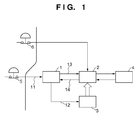
- Fig. 1 is a block diagram showing an example of the schematic arrangement of a positioning apparatus according to the present invention
- Fig. 2 is a chart showing the timing relationship between the operation statuses of a stop instruction switch, a power source, and a movable body;
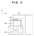
- Fig. 3 is a view for explaining an exposure apparatus.
- Fig. 1 is a block diagram showing an example of the schematic arrangement of a positioning apparatus which positions a movable body according to the present invention.
- the positioning apparatus includes a driver 2 which drives a movable body 4, a power source 3 which supplies power to the driver 2, and a controller 1 which stops the power supply from the power source 3 to the driver 2.
- the controller 1 stops the power supply from the power source 3 to the driver 2 in response to a stop instruction signal 11 which gives the instruction to stop the driving of the movable body 4.
- the movable body 4 can be an original stage 102 which holds an original such as a reticle, or a substrate stage 104 which holds a substrate in an exposure apparatus.
- the stop instruction signal 11 can be transmitted when, for example, a power shutdown switch or emergency stop switch is manipulated.
- a stop instruction switch 5 which gives the instruction to stop the driving of the movable body.
- Fig. 2 is a chart showing a power shutdown signal 12 and the operation statuses of the movable body 4 and power source 3 when the stop instruction switch 5 is pressed.
- the driver 2 In the exposure apparatus, power is supplied from the power source 3 to the driver 2 which drives the movable body 4.
- the driver 2 controls, for example, the position and velocity of the movable body 4.
- the driver 2 herein includes a linear motor, a driver, a driver power source, and a brake mechanism such as a dynamic brake, which drive the movable body 4.
- the stop instruction signal 11 which instructs the controller to stop the driving of the movable body is output to the controller 1, and a system reset signal 13 is output to the driver 2.
- the power shutdown signal 12 output from the controller 1 to the power source 3 is not enabled immediately after the stop instruction switch 5 is turned on.
- the stop instruction signal 11 is transmitted as the stop instruction switch 5 is turned on, and when it is received by the controller, the controller 1 calculates and determines a waiting time Tn in accordance with the driving status of the movable body 4 when the stop instruction switch 5 is pressed, based on a driving status signal 14 which controls the driving status of the movable body 4.
- the waiting time Tn is the time from when the controller 1 determines the waiting time Tn until it stops the power supply from the power source 3 to the driver 2.
- the power shutdown signal 12 output to the power source 3 is enabled.
- a sensor detects at least one piece of information of the position, velocity, and acceleration of the movable body 4.
- the waiting time Tn is determined based on the information detected by the sensor.
- the waiting time Tn can be, for example, the time required to decelerate the movable body 4 to a predetermined velocity at which, for example, a dynamic brake can safely stop the movable body 4.
- Japanese Patent Laid-Open No. 2001-60614 is known as a patent reference which uses a dynamic brake.
- the power source 3 continues supplying power to the driver 2 during the waiting time Tn so that the driver 2 performs brake control of the movable body 4.
- the power supply from the power source 3 to the driver 2 is stopped in response to the power shutdown signal 12 output from the controller 1.
- the dynamic brake acts on the driver 2. Then, the movable body 4 moving at the predetermined velocity or less stops without colliding against, for example, its mechanical stopper.
- the controller 1 sets the waiting time Tn in accordance with the driving status of the movable body 4. Consequently, the movable body 4 can be stopped more moderately and safely than in the prior art in accordance with its operation status. This makes it possible to suppress, for example, a drift of a linear motor movable element and to minimize the adverse influence of the stopping of the movable body 4 on, for example, a substrate on a stage.
- the controller 1 activates the dynamic brake without waiting for the waiting time Tn to stop the movable body 4.
- the exposure apparatus has an illumination device 101, an original stage 102 which carries an original, a projection optical system 103, and a substrate stage 104 which carries a substrate. At least one of the original stage 102 and the substrate stage 104 is positioned by the above-described positioning apparatus.
- the exposure apparatus projects and transfers by exposure a circuit pattern formed on the original onto a substrate, and may be of the step & repeat projection exposure type or the step & scan projection exposure type.
- the illumination device 101 illuminates a reticle on which a circuit pattern is formed, and has a light source unit and illumination optical system.
- the light source unit uses, for example, a laser as a light source.
- the laser can be, for example, an ArF excimer laser with a wavelength of about 193 nm, a KrF excimer laser with a wavelength of about 248 nm, or an F 2 excimer laser with a wavelength of about 153 nm.
- the type of laser is not particularly limited to an excimer laser and may be, for example, a YAG laser, and the number of lasers is not particularly limited either.
- the light source When a laser is used as the light source, an optical system for shaping a parallel light beam from the laser beam source into a desired beam shape, and an optical system for converting a coherent laser beam into an incoherent one are preferably used. Also, the light source which can be used for the light source unit is not particularly limited to a laser, and one or a plurality of mercury lamps or xenon lamps can be used.
- the illumination optical system illuminates a mask and includes, for example, a lens, mirror, light integrator, and stop.
- the projection optical system 103 can be, for example, an optical system having a plurality of lens elements alone, an optical system having a plurality of lens elements and at least one concave mirror, an optical system having a plurality of lens elements and at least a diffractive optical element, or an optical system having only mirrors.
- the original stage 102 and substrate stage 104 can move by, for example, a linear motor. In the step & scan projection exposure scheme, the stages 102 and 104 move synchronously. An actuator is separately provided to at least one of the substrate stage 104 and the original stage 102 to align the original pattern onto the substrate.
- the above-described exposure apparatus can be used to manufacture micropatterned devices, for example, a semiconductor device such as a semiconductor integrated circuit, a micromachine, and a thin-film magnetic head.
- a semiconductor device such as a semiconductor integrated circuit, a micromachine, and a thin-film magnetic head.
- Devices e.g., a semiconductor integrated circuit device and liquid crystal display device are manufactured by a step of exposing a substrate having a photosensitive resist layer deposited thereon to radiant energy using the exposure apparatus according to the above-described embodiment, a step of developing the resist exposed in the exposing step, and other known steps (e.g., etching, resist removing, dicing, bonding, and packaging steps) of processing the substrate developed in the developing step.
- steps e.g., etching, resist removing, dicing, bonding, and packaging steps
Landscapes
- Physics & Mathematics (AREA)
- General Physics & Mathematics (AREA)
- Exposure And Positioning Against Photoresist Photosensitive Materials (AREA)
- Exposure Of Semiconductors, Excluding Electron Or Ion Beam Exposure (AREA)
Abstract
Description
- The present invention relates to an exposure apparatus and a method of manufacturing a device.
- A process of manufacturing a semiconductor device includes a lithography step of transferring by exposure a circuit pattern formed on an original onto a substrate. In the lithography step, the original and substrate are fixed on an original stage and substrate stage, respectively, and these stages are driven in synchrony by linear motors, thereby performing exposure. Recently, in order to improve the productivity and operating ratio of such an exposure apparatus, its size and operating speed have been increased. Along with such increases in the size and speed of the exposure apparatus, a safety measure for its built-in stages is becoming complex.
- In the conventional exposure apparatus, an apparatus power source is disconnected as soon as a power shutdown signal is transmitted when a power shutdown switch or emergency stop switch is turned on. To stop a traveling stage in the exposure apparatus, a linear motor used to drive the stage is stopped by, for example, a regenerative brake.
- Japanese Patent Laid-Open No.
2001-60614 2001-60614 - In the prior art, as soon as the power shutdown switch or emergency stop switch is turned on, an apparatus power shutdown request is enabled, and the power source of the apparatus main body is stopped. After the power supply from the power source to the linear motor is stopped, the regenerative brake is activated to stop the linear motor. In this case, the linear motor may damage upon colliding against, for example, its mechanical stopper depending on the position, moving velocity, and moving direction of the stage. In particular, since a stage with high inertia is operated at high speed along with increases in the size and complexity of the exposure apparatus, the risk of such damage is increasing.
- The exposure apparatus disclosed in Japanese Patent Laid-Open No.
2001-60614 - It is an object of the present invention to provide an exposure apparatus which can safely stop a movable body irrespective of its driving status.
- According to the present invention, an exposure apparatus as defined in
claims 1 to 4 is provided. - According to the present invention, it is possible to provide an exposure apparatus which can safely stop a movable body irrespective of its driving status.
- Further features of the present invention will become apparent from the following description of exemplary embodiments with reference to the attached drawings.
-
Fig. 1 is a block diagram showing an example of the schematic arrangement of a positioning apparatus according to the present invention; -
Fig. 2 is a chart showing the timing relationship between the operation statuses of a stop instruction switch, a power source, and a movable body; and -
Fig. 3 is a view for explaining an exposure apparatus. -
Fig. 1 is a block diagram showing an example of the schematic arrangement of a positioning apparatus which positions a movable body according to the present invention. The positioning apparatus includes adriver 2 which drives amovable body 4, apower source 3 which supplies power to thedriver 2, and acontroller 1 which stops the power supply from thepower source 3 to thedriver 2. Thecontroller 1 stops the power supply from thepower source 3 to thedriver 2 in response to astop instruction signal 11 which gives the instruction to stop the driving of themovable body 4. Themovable body 4 can be anoriginal stage 102 which holds an original such as a reticle, or asubstrate stage 104 which holds a substrate in an exposure apparatus. Thestop instruction signal 11 can be transmitted when, for example, a power shutdown switch or emergency stop switch is manipulated. The power shutdown switch and emergency stop switch will be collectively referred to as astop instruction switch 5 which gives the instruction to stop the driving of the movable body.Fig. 2 is a chart showing apower shutdown signal 12 and the operation statuses of themovable body 4 andpower source 3 when thestop instruction switch 5 is pressed. - In the exposure apparatus, power is supplied from the
power source 3 to thedriver 2 which drives themovable body 4. In driving themovable body 4, thedriver 2 controls, for example, the position and velocity of themovable body 4. Thedriver 2 herein includes a linear motor, a driver, a driver power source, and a brake mechanism such as a dynamic brake, which drive themovable body 4. - In the exposure apparatus, when the
stop instruction switch 5 is turned on, thestop instruction signal 11 which instructs the controller to stop the driving of the movable body is output to thecontroller 1, and asystem reset signal 13 is output to thedriver 2. Note that thepower shutdown signal 12 output from thecontroller 1 to thepower source 3 is not enabled immediately after thestop instruction switch 5 is turned on. - The
stop instruction signal 11 is transmitted as thestop instruction switch 5 is turned on, and when it is received by the controller, thecontroller 1 calculates and determines a waiting time Tn in accordance with the driving status of themovable body 4 when thestop instruction switch 5 is pressed, based on adriving status signal 14 which controls the driving status of themovable body 4. The waiting time Tn is the time from when thecontroller 1 determines the waiting time Tn until it stops the power supply from thepower source 3 to thedriver 2. - After the waiting time Tn has elapsed, the
power shutdown signal 12 output to thepower source 3 is enabled. A sensor detects at least one piece of information of the position, velocity, and acceleration of themovable body 4. The waiting time Tn is determined based on the information detected by the sensor. The waiting time Tn can be, for example, the time required to decelerate themovable body 4 to a predetermined velocity at which, for example, a dynamic brake can safely stop themovable body 4. Japanese Patent Laid-Open No.2001-60614 - Even after the
stop instruction switch 5 is turned on, thepower source 3 continues supplying power to thedriver 2 during the waiting time Tn so that thedriver 2 performs brake control of themovable body 4. When themovable body 4 reaches the predetermined velocity or less after the waiting time Tn has elapsed, the power supply from thepower source 3 to thedriver 2 is stopped in response to thepower shutdown signal 12 output from thecontroller 1. - When the power supply from the
power source 3 to thedriver 2 is stopped as thepower source 3 is turned off, the dynamic brake acts on thedriver 2. Then, themovable body 4 moving at the predetermined velocity or less stops without colliding against, for example, its mechanical stopper. - When a
reset switch 6 is turned on, the power supply from thepower source 3 to thedriver 2 continues during the waiting time Tn, as in the case in which thestop instruction switch 5 is turned on. After the elapse of the waiting time Tn, the driver power source in thedriver 2 is stopped, and the dynamic brake acts on thedriver 2 to safely stop themovable body 4. Note that the power supply from thepower source 3 to thedriver 2 is not stopped even after the elapse of the waiting time Tn, unlike the case in which thestop instruction switch 5 is turned on. - In this embodiment, the
controller 1 sets the waiting time Tn in accordance with the driving status of themovable body 4. Consequently, themovable body 4 can be stopped more moderately and safely than in the prior art in accordance with its operation status. This makes it possible to suppress, for example, a drift of a linear motor movable element and to minimize the adverse influence of the stopping of themovable body 4 on, for example, a substrate on a stage. - In this embodiment, if an abnormality is detected in the power supply of the
power source 3, thecontroller 1 activates the dynamic brake without waiting for the waiting time Tn to stop themovable body 4. - Although the above description has been given assuming that only one
movable body 4 is present, the present invention can be applied even when a plurality ofmovable bodies 4 are present. - [Embodiment of Exposure Apparatus] An exemplary exposure apparatus to which the positioning apparatus according to the present invention is applied will now be described. As shown in
Fig. 3 , the exposure apparatus has anillumination device 101, anoriginal stage 102 which carries an original, a projectionoptical system 103, and asubstrate stage 104 which carries a substrate. At least one of theoriginal stage 102 and thesubstrate stage 104 is positioned by the above-described positioning apparatus. The exposure apparatus projects and transfers by exposure a circuit pattern formed on the original onto a substrate, and may be of the step & repeat projection exposure type or the step & scan projection exposure type. - The
illumination device 101 illuminates a reticle on which a circuit pattern is formed, and has a light source unit and illumination optical system. The light source unit uses, for example, a laser as a light source. The laser can be, for example, an ArF excimer laser with a wavelength of about 193 nm, a KrF excimer laser with a wavelength of about 248 nm, or an F2 excimer laser with a wavelength of about 153 nm. However, the type of laser is not particularly limited to an excimer laser and may be, for example, a YAG laser, and the number of lasers is not particularly limited either. When a laser is used as the light source, an optical system for shaping a parallel light beam from the laser beam source into a desired beam shape, and an optical system for converting a coherent laser beam into an incoherent one are preferably used. Also, the light source which can be used for the light source unit is not particularly limited to a laser, and one or a plurality of mercury lamps or xenon lamps can be used. - The illumination optical system illuminates a mask and includes, for example, a lens, mirror, light integrator, and stop. The projection
optical system 103 can be, for example, an optical system having a plurality of lens elements alone, an optical system having a plurality of lens elements and at least one concave mirror, an optical system having a plurality of lens elements and at least a diffractive optical element, or an optical system having only mirrors. - The
original stage 102 andsubstrate stage 104 can move by, for example, a linear motor. In the step & scan projection exposure scheme, thestages substrate stage 104 and theoriginal stage 102 to align the original pattern onto the substrate. - The above-described exposure apparatus can be used to manufacture micropatterned devices, for example, a semiconductor device such as a semiconductor integrated circuit, a micromachine, and a thin-film magnetic head.
- A method of manufacturing a device using the above-described exposure apparatus will be exemplified next.
- Devices (e.g., a semiconductor integrated circuit device and liquid crystal display device) are manufactured by a step of exposing a substrate having a photosensitive resist layer deposited thereon to radiant energy using the exposure apparatus according to the above-described embodiment, a step of developing the resist exposed in the exposing step, and other known steps (e.g., etching, resist removing, dicing, bonding, and packaging steps) of processing the substrate developed in the developing step.
- While the present invention has been described with reference to exemplary embodiments, it is to be understood that the invention is not limited to the disclosed exemplary embodiments. The scope of the following claims is to be accorded the broadest interpretation so as to encompass all such modifications and equivalent structures and functions.
Claims (5)
- An exposure apparatus for projecting a pattern image of an original onto a substrate, the exposure apparatus comprising a projection optical system (103), positioning means operable to position a movable body (4) including one or more of: an original stage (102) configured to hold the original; and a substrate stage (104) configured to hold the substrate, characterized in that the positioning means comprises:drive means (2) configured to drive the movable body (4);a power source (3) configured to supply power to said driver (2); anda controller (1) configured to stop the power supply from said power source (3) to said drive means (2) after a time period elapses in response to a received stop instruction signal to stop the driving of the movable body (4), the time period being determined in accordance with a driving status of the movable body (4) driven by said drive means (2).
- The exposure apparatus according to claim 1, wherein the positioning apparatus further comprises a sensor configured to detect information comprising one or more of: the position, velocity, and acceleration of the movable body (4),
wherein said controller (1) is operable to determine the time period based on the detected information. - The exposure apparatus according to claim 1 or 2, in which the stop instruction signal (11) is transmitted in accordance with operation of a switch (5) configured to instruct to stop said driver (2).
- The exposure apparatus according to any one of claims 1 to 3, in which
said drive means (2) includes a dynamic brake, and
said controller (1) is operable to activate said dynamic brake in response to detection of an abnormality in the power being supplied by said power source (3). - A method of manufacturing a device, the method characterized by comprising: exposing a substrate to radiant energy using an exposure apparatus defined in any one of claims 1 to 4; developing the exposed substrate; and processing the developed substrate to manufacture the device.
Applications Claiming Priority (1)
| Application Number | Priority Date | Filing Date | Title |
|---|---|---|---|
| JP2007205848A JP2009043852A (en) | 2007-08-07 | 2007-08-07 | Positioning apparatus, exposure apparatus, and device manufacturing method |
Publications (1)
| Publication Number | Publication Date |
|---|---|
| EP2023206A1 true EP2023206A1 (en) | 2009-02-11 |
Family
ID=39870019
Family Applications (1)
| Application Number | Title | Priority Date | Filing Date |
|---|---|---|---|
| EP08162028A Withdrawn EP2023206A1 (en) | 2007-08-07 | 2008-08-07 | Exposure apparatus and device manufacturing method |
Country Status (5)
| Country | Link |
|---|---|
| US (1) | US7639344B2 (en) |
| EP (1) | EP2023206A1 (en) |
| JP (1) | JP2009043852A (en) |
| KR (1) | KR100990410B1 (en) |
| TW (1) | TW200919110A (en) |
Families Citing this family (1)
| Publication number | Priority date | Publication date | Assignee | Title |
|---|---|---|---|---|
| NL2004401A (en) * | 2009-04-15 | 2010-10-18 | Asml Netherlands Bv | Lithographic apparatus, positioning system, and positioning method. |
Citations (5)
| Publication number | Priority date | Publication date | Assignee | Title |
|---|---|---|---|---|
| US5040431A (en) * | 1988-01-22 | 1991-08-20 | Canon Kabushiki Kaisha | Movement guiding mechanism |
| JPH07191757A (en) * | 1993-12-24 | 1995-07-28 | Canon Inc | Positioning stage device |
| JPH07328966A (en) * | 1994-06-07 | 1995-12-19 | Fanuc Ltd | Brake control system for robot |
| JP2001060614A (en) | 1999-06-15 | 2001-03-06 | Canon Inc | Semiconductor manufacturing apparatus and semiconductor device manufacturing method |
| US6566770B1 (en) * | 1999-06-15 | 2003-05-20 | Canon Kabushiki Kaisha | Semiconductor manufacturing apparatus and device manufacturing method |
Family Cites Families (4)
| Publication number | Priority date | Publication date | Assignee | Title |
|---|---|---|---|---|
| JPH07321024A (en) * | 1994-05-25 | 1995-12-08 | Canon Inc | Positioning method and apparatus therefor and exposure apparatus using the same |
| JPH0878506A (en) * | 1994-09-05 | 1996-03-22 | Canon Inc | Positioning control device |
| JP2000228342A (en) | 1999-02-04 | 2000-08-15 | Canon Inc | Exposure equipment |
| JP4266260B2 (en) * | 1999-12-08 | 2009-05-20 | 西部電機株式会社 | Method for emergency stop of an article cutting and conveying apparatus |
-
2007
- 2007-08-07 JP JP2007205848A patent/JP2009043852A/en active Pending
-
2008
- 2008-08-04 US US12/185,272 patent/US7639344B2/en not_active Expired - Fee Related
- 2008-08-06 TW TW097129848A patent/TW200919110A/en unknown
- 2008-08-06 KR KR1020080076853A patent/KR100990410B1/en not_active Expired - Fee Related
- 2008-08-07 EP EP08162028A patent/EP2023206A1/en not_active Withdrawn
Patent Citations (5)
| Publication number | Priority date | Publication date | Assignee | Title |
|---|---|---|---|---|
| US5040431A (en) * | 1988-01-22 | 1991-08-20 | Canon Kabushiki Kaisha | Movement guiding mechanism |
| JPH07191757A (en) * | 1993-12-24 | 1995-07-28 | Canon Inc | Positioning stage device |
| JPH07328966A (en) * | 1994-06-07 | 1995-12-19 | Fanuc Ltd | Brake control system for robot |
| JP2001060614A (en) | 1999-06-15 | 2001-03-06 | Canon Inc | Semiconductor manufacturing apparatus and semiconductor device manufacturing method |
| US6566770B1 (en) * | 1999-06-15 | 2003-05-20 | Canon Kabushiki Kaisha | Semiconductor manufacturing apparatus and device manufacturing method |
Also Published As
| Publication number | Publication date |
|---|---|
| TW200919110A (en) | 2009-05-01 |
| KR20090014991A (en) | 2009-02-11 |
| KR100990410B1 (en) | 2010-10-29 |
| JP2009043852A (en) | 2009-02-26 |
| US20090040499A1 (en) | 2009-02-12 |
| US7639344B2 (en) | 2009-12-29 |
Similar Documents
| Publication | Publication Date | Title |
|---|---|---|
| US20100002212A1 (en) | Scanning exposure apparatus, exposure method, and device manufacturing method | |
| US20090002659A1 (en) | Stage apparatus, exposure apparatus, and method of manufacturing device | |
| JP4621647B2 (en) | Lithographic apparatus and device manufacturing method | |
| US7619330B2 (en) | Stage apparatus | |
| US7639344B2 (en) | Exposure apparatus and method of manufacturing device | |
| JP2009004775A (en) | Lithographic apparatus and pivotable structure assembly | |
| JP2019532324A (en) | Positioning system and lithographic apparatus | |
| US7280182B2 (en) | Lithographic apparatus, device manufacturing method and computer program | |
| JP2012004201A (en) | Mobile device, exposure device, device manufacturing method, flat panel display manufacturing method and mobile device control method | |
| JP4938878B2 (en) | Lithographic apparatus, positioning system, and positioning method | |
| KR101784045B1 (en) | Exposure apparatus and method of manufacturing article | |
| US8134686B2 (en) | Immersion exposure apparatus and device manufacturing method | |
| JPH06204115A (en) | Projection exposure apparatus and exposure method | |
| JP4854628B2 (en) | Lithographic apparatus and device manufacturing method | |
| JP7022527B2 (en) | Stage equipment, lithography equipment, and article manufacturing methods | |
| JP2001244175A (en) | Exposure method and exposure apparatus, mask, and device manufacturing method | |
| US7990518B2 (en) | Immersion exposure apparatus and device manufacturing method | |
| JP2010161235A (en) | Positioning apparatus, exposing device, method of manufacturing device | |
| JP7352332B2 (en) | exposure equipment | |
| JP2009043852A5 (en) | ||
| JP5053884B2 (en) | Stage apparatus and exposure apparatus | |
| KR20240131892A (en) | Stage apparatus, lithography apparatus, substrate delivery method, and article manufacturing method | |
| JP2001007009A (en) | Positioning method, positioning apparatus and projection exposure apparatus using the same | |
| JP2006287121A (en) | Positioning apparatus and control method thereof | |
| JPS62189509A (en) | Drive controller |
Legal Events
| Date | Code | Title | Description |
|---|---|---|---|
| PUAI | Public reference made under article 153(3) epc to a published international application that has entered the european phase |
Free format text: ORIGINAL CODE: 0009012 |
|
| AK | Designated contracting states |
Kind code of ref document: A1 Designated state(s): AT BE BG CH CY CZ DE DK EE ES FI FR GB GR HR HU IE IS IT LI LT LU LV MC MT NL NO PL PT RO SE SI SK TR |
|
| AX | Request for extension of the european patent |
Extension state: AL BA MK RS |
|
| 17P | Request for examination filed |
Effective date: 20090811 |
|
| AKX | Designation fees paid |
Designated state(s): AT BE BG CH CY CZ DE DK EE ES FI FR GB GR HR HU IE IS IT LI LT LU LV MC MT NL NO PL PT RO SE SI SK TR |
|
| STAA | Information on the status of an ep patent application or granted ep patent |
Free format text: STATUS: THE APPLICATION HAS BEEN WITHDRAWN |
|
| 18W | Application withdrawn |
Effective date: 20100811 |