EP2019487B1 - Switching circuitry - Google Patents
Switching circuitry Download PDFInfo
- Publication number
- EP2019487B1 EP2019487B1 EP20070113380 EP07113380A EP2019487B1 EP 2019487 B1 EP2019487 B1 EP 2019487B1 EP 20070113380 EP20070113380 EP 20070113380 EP 07113380 A EP07113380 A EP 07113380A EP 2019487 B1 EP2019487 B1 EP 2019487B1
- Authority
- EP
- European Patent Office
- Prior art keywords
- clock
- switch
- mask
- circuitry
- signal
- Prior art date
- Legal status (The legal status is an assumption and is not a legal conclusion. Google has not performed a legal analysis and makes no representation as to the accuracy of the status listed.)
- Active
Links
- 230000000295 complement effect Effects 0.000 claims description 32
- 230000000630 rising effect Effects 0.000 claims description 15
- 101100269850 Caenorhabditis elegans mask-1 gene Proteins 0.000 description 32
- 239000000872 buffer Substances 0.000 description 8
- 102100036822 Ankyrin repeat and KH domain-containing protein 1 Human genes 0.000 description 6
- 101000928335 Homo sapiens Ankyrin repeat and KH domain-containing protein 1 Proteins 0.000 description 6
- 238000006243 chemical reaction Methods 0.000 description 6
- 101100115778 Caenorhabditis elegans dac-1 gene Proteins 0.000 description 4
- 230000003213 activating effect Effects 0.000 description 3
- 230000001419 dependent effect Effects 0.000 description 3
- 238000010586 diagram Methods 0.000 description 3
- 238000000034 method Methods 0.000 description 3
- 230000003071 parasitic effect Effects 0.000 description 3
- 230000001934 delay Effects 0.000 description 2
- 230000000694 effects Effects 0.000 description 2
- 102100034609 Ankyrin repeat domain-containing protein 17 Human genes 0.000 description 1
- 101000924481 Homo sapiens Ankyrin repeat domain-containing protein 17 Proteins 0.000 description 1
- 230000005669 field effect Effects 0.000 description 1
- 238000001914 filtration Methods 0.000 description 1
- 230000002040 relaxant effect Effects 0.000 description 1
- 230000001960 triggered effect Effects 0.000 description 1
Images


Classifications
-
- H—ELECTRICITY
- H03—ELECTRONIC CIRCUITRY
- H03K—PULSE TECHNIQUE
- H03K17/00—Electronic switching or gating, i.e. not by contact-making and –breaking
- H03K17/16—Modifications for eliminating interference voltages or currents
-
- H—ELECTRICITY
- H03—ELECTRONIC CIRCUITRY
- H03M—CODING; DECODING; CODE CONVERSION IN GENERAL
- H03M1/00—Analogue/digital conversion; Digital/analogue conversion
- H03M1/06—Continuously compensating for, or preventing, undesired influence of physical parameters
- H03M1/0614—Continuously compensating for, or preventing, undesired influence of physical parameters of harmonic distortion
-
- H—ELECTRICITY
- H03—ELECTRONIC CIRCUITRY
- H03M—CODING; DECODING; CODE CONVERSION IN GENERAL
- H03M1/00—Analogue/digital conversion; Digital/analogue conversion
- H03M1/06—Continuously compensating for, or preventing, undesired influence of physical parameters
- H03M1/0617—Continuously compensating for, or preventing, undesired influence of physical parameters characterised by the use of methods or means not specific to a particular type of detrimental influence
- H03M1/0624—Continuously compensating for, or preventing, undesired influence of physical parameters characterised by the use of methods or means not specific to a particular type of detrimental influence by synchronisation
-
- H—ELECTRICITY
- H03—ELECTRONIC CIRCUITRY
- H03M—CODING; DECODING; CODE CONVERSION IN GENERAL
- H03M1/00—Analogue/digital conversion; Digital/analogue conversion
- H03M1/06—Continuously compensating for, or preventing, undesired influence of physical parameters
- H03M1/0617—Continuously compensating for, or preventing, undesired influence of physical parameters characterised by the use of methods or means not specific to a particular type of detrimental influence
- H03M1/0634—Continuously compensating for, or preventing, undesired influence of physical parameters characterised by the use of methods or means not specific to a particular type of detrimental influence by averaging out the errors, e.g. using sliding scale
- H03M1/0656—Continuously compensating for, or preventing, undesired influence of physical parameters characterised by the use of methods or means not specific to a particular type of detrimental influence by averaging out the errors, e.g. using sliding scale in the time domain, e.g. using intended jitter as a dither signal
- H03M1/066—Continuously compensating for, or preventing, undesired influence of physical parameters characterised by the use of methods or means not specific to a particular type of detrimental influence by averaging out the errors, e.g. using sliding scale in the time domain, e.g. using intended jitter as a dither signal by continuously permuting the elements used, i.e. dynamic element matching
- H03M1/0663—Continuously compensating for, or preventing, undesired influence of physical parameters characterised by the use of methods or means not specific to a particular type of detrimental influence by averaging out the errors, e.g. using sliding scale in the time domain, e.g. using intended jitter as a dither signal by continuously permuting the elements used, i.e. dynamic element matching using clocked averaging
-
- H—ELECTRICITY
- H03—ELECTRONIC CIRCUITRY
- H03M—CODING; DECODING; CODE CONVERSION IN GENERAL
- H03M1/00—Analogue/digital conversion; Digital/analogue conversion
- H03M1/66—Digital/analogue converters
- H03M1/74—Simultaneous conversion
- H03M1/742—Simultaneous conversion using current sources as quantisation value generators
- H03M1/747—Simultaneous conversion using current sources as quantisation value generators with equal currents which are switched by unary decoded digital signals
Definitions
- the present invention relates to switching circuitry for use, for example, in high-speed digital-to-analog converters (DACs).
- DACs digital-to-analog converters
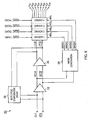
- Figure 1 shows an overview of a previously considered DAC.
- the DAC in Figure 1 is part of a DAC integrated circuit (IC) of the current-steering type, and is designed to convert an m-bit digital input word (D1-Dm) into a corresponding analog output signal.
- IC DAC integrated circuit
- the analog circuitry further includes a number n of differential switching circuits 4 1 to 4 n corresponding respectively to the n current sources 2 1 to 2 n .
- Each differential switching circuit 4 is connected to its corresponding current source 2 and switches the current I produced by the current source either to a first terminal, connected to a first connection line A of the converter, or a second terminal connected to a second connection line B of the converter.
- Each differential switching circuit 4 receives one of a plurality of digital control signals T1 to Tn (called “thermometer-coded signals” for reasons explained hereinafter) and selects either its first terminal or its second terminal in accordance with the value of the signal concerned.
- a first output current I A of the DAC 1 is the sum of the respective currents delivered to the first terminals of the differential switching circuit
- a second output current I B of the DAC 1 is the sum of the respective currents delivered to the second terminals of the differential switching circuit.
- the analog output signal is the voltage difference V A -V B between a voltage V A produced by sinking the first output current I A of the DAC 1 into a resistance R and a voltage V B produced by sinking the second output current I B of the converter into another resistance R.
- thermometer-coded signals T1 to Tn are derived from the binary input word D1-Dm by digital circuitry including a binary-thermometer decoder 6.
- thermometer-coded signals T1 to Tn produced by the decoder 6 are such that more of the differential switching circuits select their respective first terminals (starting from the differential switching circuit 4 1 ) without any differential switching circuit that has already selected its first terminal switching back to its second terminal.
- the first i differential switching circuits 4 1 to 4 i select their respective first terminals, whereas the remaining n-i differential switching circuits 4 i+1 to 4 n select their respective second terminals.
- the analog output signal V A -V B is equal to (2i-n)IR.
- Thermometer coding is popular in DACs of the current-steering type because, as the binary input word increases, more current sources are switched to the first connection line A without any current source that is already switched to that line A being switched to the other line B. Accordingly, the input/output characteristic of the DAC is monotonic and the glitch impulse resulting from a change of 1 in the input word is small.
- FIG. 2 An exemplary differential switching circuit suitable for use with the DAC of Figure 1 is shown in Figure 2 .
- This differential switching circuit comprises first and second PMOS field-effect transistors (FETs) S1 and S2.
- the respective sources of the transistors S1 and S2 are connected to a common node TAIL to which a corresponding current source (2 1 to 2 n in Figure 1 ) is connected.
- the respective drains of the transistors S1 and S2 are connected to respective first and second output nodes OUTA and OUTB of the circuit which correspond respectively to the first and second terminals of each of the differential switching circuits shown in Figure 1 .
- Each transistor S1 and S2 has a corresponding driver circuit 8 1 or 8 2 connected to its gate.
- Complementary input signals IN and INB are applied respectively to the inputs of the driver circuits 8 1 and 8 2 .
- Each driver circuit buffers and inverts its received input signal IN or INB to produce a switching signal SW1 or SW2 for its associated transistor S1 or S2 such that, in the steady-state condition, one of the transistors S1 and S2 is on and the other is off.
- Third order distortion is particularly undesirable in DACs which produce multi-tone output signals, since third order intermodulation distortion may occur in-band, in which case it cannot be removed by filtering. Such third order distortion is believed to be due in part to currents flowing into and out of parasitic capacitances which are present in the differential switching circuits ( Figure 2 ).
- This differential switching circuit 10 differs from the differential switching circuit of Figure 2 in that it has two FETs associated with each output node OUTA and OUTB.
- the first and third FETs S1 and S3 are connected between a first output node OUTA and a common node TAIL.
- the second and fourth FETs S2 and S4 are connected between a second output node OUTB and the common node TAIL.
- Each of these four FETs S1 to S4 is turned on or off by a drive signal V S1 to V S4 applied thereto.
- the differential switching circuit 10 of Figure 3 is designed to operate in alternating first and second phases, which may be referred to odd and even phases.
- the first and second FETs S1 and S2 constitute a first pair of FETs which are available in each odd phase.
- the third and fourth FETs S3 and S4 constitute a second pair of FETs which are available in each even phase.
- In each odd phase one of the FETs of the pair S1 and S2 is turned on and the other of those FETs is turned off. Both transistors of the second pair (S3 and S4) are off.
- In each even phase one FET of the pair S3 and S4 is turned on and the other is turned off.
- the two FETs of the first pair S1 and S2 are both off.
- the FET which is turned on in a pair is determined by the data applied to the DAC, as will be explained later.
- the advantage of the Figure 3 differential switching circuit 10 is that at the start of each odd or even phase the same number of FETs change state. One FET will always be turning on and another FET will always be turning off. For example, consider the case in which S1 is on in an odd phase and then in the next even phase the data remains unchanged. In that case, at the start of the even phase concerned, S1 turns off and S3 turns on, S2 and S4 remaining off. In the Figure 2 differential switch circuit, this is not possible, the switch S1 simply remaining on in successive cycles when the data is unchanged. This means that in the Figure 2 circuit, the number of FETs that change state from one cycle to the next is dependent on the data.
- the number of FETs that change state from one phase to the next is independent of the data.
- the charge which flows into and out of the parasitic capacitances in the circuitry is less dependent on the input data signal. This helps to reduce third order distortion which may occur in the analog output signal.
- Timing mis-matches between different analog segments and between different switching parts of the same segment.
- circuit problems will arise if the signals IN and INB applied to one analog segment change at times different from the corresponding signals in other analog segments.
- a problem still arises if the two different switch drivers 8 1 and 8 2 have timing mismatches between them.
- Such timing mismatches can arise, for example, due to random threshold voltage variations between FETs used to implement the drivers 8 1 and 8 2 .
- the phenomenon of random threshold variation becomes more significant as the transistor sizes are reduced in order to improve the switching speeds of the transistors.
- EP-A-1720258 modified switch driver circuitry as shown in Figure 4 .
- This modified switch driver circuitry 12 is connected to the differential switch circuit 10 of Figure 3 , and supplies the drive signals V S1 to V S4 FETs S1 to S4 in the differential switching circuit 10.
- the Figure 3 switch driver circuitry comprises first and second circuits 14 and 16. Each circuit has a clock input node at which one of a pair of complementary clock signals CLK ODD and CLK EVEN is received. Each circuit 14 and 16 also has first and second output nodes. These two output nodes are connected respectively to the gates of the two FETs of a pair of FETs in Figure 3 . For example, in the case of the first circuit 14, the first output node is connected to the gate of S1 of the first pair of FETs and the second output node is connected to the gate of S2 in the first pair.
- the first output node of the second circuit 16 is connected to the gate of S3 in the second pair of FETs S3 and S4, and the second output node of the second circuit 16 is connected to the gate of S4.
- Each of the first and second circuits 14 and 16 comprises a switch SW8/SW4 connected between the clock input node and the first output node, and a switch SW7/SW3 connected between the clock input node and the second output node.
- Each of the first and second circuits 14 and 16 also has a pair of data input nodes at which respective complementary thermometer-coded data signals are received.
- the complementary data signals are the signals T ODD and T ODD .
- the complementary data signals are the signals T EVEN and T EVEN .
- the complementary data signals T ODD and T ODD for the first circuit 14 are generated by a first decoder of the DAC.
- the complementary data signals T EVEN and T EVEN for the second circuit 16 are generated by a second decoder, separate from the first decoder. Each of these decoders carries out a binary-thermometer decoding operation.
- the frequency of the decoding operations performed by each decoder need only be half the frequency of the conversion cycles of the DAC. This can be useful for reducing power consumption of the decoding circuitry. It may also be useful where the DAC conversion frequency is so high that carrying out decoding operations at the DAC conversion frequency using a single decoder is problematic.
- Each of the first and second circuits 14 and 16 further comprises a switch SW6/SW2 connected between the first output node and a positive supply line V DD , and a switch SW5/SW1 connected between the second output node and V DD .
- the switches SW6 and SW7 in the first circuit 14 are both controlled by the inverted data signal T ODD .
- the switches SW5 and SW8 in the first circuit 14 are both controlled by the data signal T ODD .
- the switches SW2 and SW3 in the second circuit 16 are both controlled by the inverted data signal T EVEN .
- the switches SW1 and SW4 in the second circuit 16 are both controlled by the data signal T EVEN .
- the clock signal CLK ODD is active (low) and the clock signal CLK EVEN is inactive (high) in each odd phase.
- the clock signals CLK ODD and CLK EVEN are inactive (high) and active (low) in each even-numbered phase. Any changes to the data signals applied to either circuit 14 and 16 are made when the clock signal applied to the clock node of the circuit concerned is in the inactive (high) state. In other words, any change in the data signals T ODD and T ODD are made only in even phases when CLK ODD is inactive (high). Similarly, any changes in the data signals T EVEN and T EVEN are made only in odd phases, i.e. when CLK EVEN is inactive (high).
- the switch driver circuitry 12 in Figure 4 is effective in reducing the effect of switching delay mismatches.
- the present applicants are now contemplating a DAC capable of operating at a much higher conversion frequency, for example up to 12 Gsamples/s. This imposes some severe requirements on the circuitry.
- One way of relaxing these requirements is to increase the number of phases beyond two. This enables the decoders to have longer to carry out their decoding operations. For example, it might be contemplated to provide four pairs of switches in the differential switching circuit, instead of the two pairs shown in Figure 3 , and four circuits in the switch driver circuitry of Figure 4 , instead of the two circuits 14 and 16.
- the switch driver circuitry 12 of Figure 4 it would be necessary to increase the number of clock signals from 2 to 4 as well. These four clock signals would need to be 90° out of phase with one another. Generating and delivering such multiphase clock signals to all of the different segments would be very difficult to do in practice.
- the clock signals are used directly to provide the drive signals to the FETs in the differential switching circuitry. It follows that any timing errors in the clock signals will affect the performance of the differential switching circuitry directly.
- switch driver circuitry as defined in independent claim 1, to which the reader should now refer.
- Optional features are defined in the dependent claims.
- Each said driver circuit may also comprise means for maintaining said output node at a predetermined potential when the clock switch is off, said predetermined potential preferably being substantially equal to the potential of the clock signal received at said clock input node prior to said preselected change.
- the maintaining means may comprise a further switch connected between said output node and a source of said predetermined potential, said switch controller preferably being operable to turn on said further switch when said clock switch is turned off.
- the driver circuit also has a data input node at which a data signal is received, and the switch controller is preferably operable to employ the data signal to determine whether or not to turn on the clock switch during said active period of the received mask signal.
- Each said driver circuit may have first and second output nodes and first and second clock switches, said first clock switch being connected between said clock input node and said first output node and said second clock switch being connected between said clock input node and said second output node, and the switch controller may be operable to select one of the first and second clock switches in dependence upon said data signal and to turn on the selected clock switch in advance of said preselected change.
- the switch controller may comprise a latch connected for receiving said data signal and a signal complementary thereto and also connected for receiving said mask signal, the latch having a first output connected to a control terminal of said first clock switch and a second output connected to a control terminal of said second clock switch, the latch being arranged so that during said inactive period of the mask signal the first and second outputs are both in an OFF state, in which the first and second clock signals are off and so that, at the start of each active period of the mask signal, one of the first and second outputs changes from an OFF state to an ON state, in which said one clock switch is turned ON, and the other of the two outputs remains in the OFF state, the first and second outputs remaining unchanged if the data input changes subsequently during the active period concerned.
- the mask generator circuit may be operable to cause said active period of the mask signal received by each said driver circuit to begin prior to a first preselected change in the clock signal received at the clock input node of the driver circuit concerned and to end after a second preselected change in that clock signal.
- the first and second preselected changes may be successive edges of the clock signal concerned, one of the edges being a rising edge and the other of the edges being a falling edge.
- Any changes in the data signal at the data input node of one of the driver circuits may be made during an inactive period of the mask signal received at the mask input node of the driver circuit concerned.
- the circuitry may further comprise means for adjusting a duty cycle of said one or more clock signals applied to the mask generating circuit.
- switching circuitry comprising: switch driver circuitry according to the aforementioned first aspect of the present invention; and a switching circuit having a plurality of switchable elements, each connected to one of the said output nodes of the switch driver circuitry for receiving respective drive signals therefrom.
- the switching circuit may be a differential switching circuit having a common node and first and second switch nodes, the plurality of switchable elements being operable to connect the common node to a selected one of the first and second switch nodes in each of said phases.
- the number of switchable elements which change state from one phase to the next is constant.
- a digital-to-analog converter comprising switching circuitry according to the aforementioned second aspect of the present invention.
- an IC chip or chipset comprising switch driver circuitry according to the aforementioned first aspect of the present invention, or comprising switching circuitry according to the aforementioned second aspect of the present invention, or comprising a digital-to-analog converter according to the aforementioned third aspect of the present invention.
- a circuit board comprising switch driver circuitry according to the aforementioned first aspect of the present invention, or comprising switching circuitry according to the aforementioned second aspect of the present invention, or comprising a digital-to-analog converter according to the aforementioned third aspect of the present invention.
- an RF transmitter comprising a digital-to-analogue converter according to the aforementioned third aspect of the present invention.
- Such an RF transmitter may be part of a base station, relay station or a mobile device, and accordingly the present invention extends to this equipment too.
- Figure 5 shows parts of a DAC embodying the present invention.
- the DAC is intended to have a conversion frequency of up to 12 G samples/s.
- Such a DAC may be used, for example, to synthesise a radio-frequency (RF) signal in a mobile telephone base station.
- the DAC is segmented and has a plurality of analog segments in the same basic manner as the DAC of Figure 1 .
- the parts of the DAC shown in Figure 5 are mainly parts of the analog circuitry of the DAC.
- the DAC also comprises digital circuitry that is not shown in Figure 5 .
- This digital circuitry for example, includes an array of decoders (for example 16 decoders), each of which carries out binary-to-thermometer decoding operations. With 16 decoders and a DAC conversion frequency of 12 G samples/s, each individual decoder is required to perform 750 million decoding operations per second.
- the DAC analog circuitry comprises four multiplexer/retiming circuits 20 1 to 20 4 .
- Each of these multiplexer/retiming circuits 20 1 to 20 4 receives the decoded data signals produced by four of the decoders of the decoder array.
- Each multiplexer/retiming circuit performs time-division multiplexing on the decoded data signals received from its four decoders to produce a stream of multiplexed data signals.
- the data signals are of the complementary type, and also there is one pair of complementary data signals per analog segment. For simplicity in Figure 5 , only one such pair of complementary data signals is shown.
- the complementary data signals produced by the multiplexer/retiming circuit it 20 1 are the signals DATA 1 and DATA1
- the complementary data signals produced by the multiplexer/retiming circuit 20 2 are the signals DATA 2 and DATA2
- the complementary data signals produced by the multilplexer/retiming circuit 20 3 are the signals DATA 3 and DATA3
- the complementary data signals produced by the multiplexer/retiming circuit 20 4 are the signals DATA 4 and DATA4 . Changes in each of these pairs of complementary data signals occur at a frequency of 3 GHz.
- the four pairs of complementary data signals are supplied from the multiplexer/retiming circuits 20 1 to 20 4 to switch driver circuitry 22.
- the switch driver circuitry 22 also receives a pair of complementary clock signals CLK and CLK from a clock circuit 24.
- the frequency of each of the clock signals CLK and CLK is 6 GHz.
- the switch driver circuitry 22 is segmented into n segments. Each of the segments receives the four pairs of complementary data signals (DATA 1 to DATA 4 and DATA1 to DATA4 ). Each segment derives from the received complementary data-signal parts and the complementary clock signals CLK and CLK a set of 8 drive signals V S1 to V S8 .
- the analog circuitry in Figure 5 further comprises differential switching circuitry 26 which is also segmented into n segments.
- Each segment of the differential switching circuitry receives the 8 drive signals V S1 to V S8 produced by the corresponding segment of the switch driver circuitry 22 and produces an analog output signal for its segments.
- the respective analog output signals of the n segments of the differential switching circuitry 26 are then combined together to produce an analog output signal for the DAC.
- changes in the analog output signal can occur at 12 GHz.
- Figure 6 shows the circuitry in one segment of the switch driver circuitry 22 of Figure 5 .
- the segment 30 comprises a buffer 32, a level shift and edge control circuit 34, a duty cycle compensation circuit 36, a mask generator circuit 38 and first to fourth driver circuits 40 1 to 40 4 .
- the buffer 32 receives the pair of complementary clock signals CLK and CLK from the clock circuit 24 in Figure 5 .
- the buffer 32 amplifies the received clock signals and supplies buffered complementary clock signals BCLK and BCLK to the level shift and edge control circuit 34.
- Circuit 34 adjusts the voltage levels and edge timings of the complementary clock signals as necessary and supplies the resulting adjusted clock signals LCLK and LCLK to the driver circuits 40 1 to 40 4 .
- the duty cycle compensation circuit 36 is connected to the inputs of the buffer 32 and the outputs of the level shift and edge control circuit 34.
- the duty cycle compensation circuit 36 adjusts the duty cycle of the clock signals so that the adjusted clock signals LCLK and LCLK supplied to the driver circuits 40 1 and 40 4 have a 50% duty cycle.
- the clock signals CLK and CLK may be generated off-chip and AC-coupled onto the chip.
- the clock paths for CLK and CLK may have an on-chip centre-tapped termination resistor.
- the duty cycle compensation circuit may then operate to adjust the common-node voltage of the clock signals CLK and CLK .
- This can be achieved by adding a voltage difference to the differential clock signals, for example by adjusting the equivalent termination voltages of the differential clock signals.
- the adjustment can be carried out in many different ways. For example, it is possible to move each actual termination voltage (these being driven from the amplifiers).
- the split resistors may be 55 ⁇ and 500 ⁇ . These possibilities are all equivalent to adding an input offset voltage to the differential clock signal to move the crossovers in opposite directions.
- the clock signals CLK and CLK may be approximately sinusoidal at the intended operating frequencies.
- the buffered clock signals BCLK and BCLK produced by the buffer 32 are also applied to the mask generator circuit 38.
- the mask generator circuit derives first to fourth mask signals MASK 1, MASK 2, MASK 3 and MASK 4 from the buffered clock signals and supplies them respectively to the first to fourth driver circuits 40 1 to 40 4 .
- the mask signals each have a frequency of half the frequency of the clock signals CLK and CLK .
- the different mask signals are 90° out of phase with one another.
- FIG 7 shows one example implementation of the mask generator 38 in Figure 6 .
- the mask generator 38 comprises first and second flip-flops 50 and 52. Each flip-flop has its Q output connected to its D input. Accordingly, each flip-flop operates as a divide-by-two circuit.
- the first flip-flop 50 receives at its clock input the buffered clock signal BCLK. This flip-flop generates at its Q output the first mask signal MASK 1 and generates at its Q output the third mask signal MASK 3. Accordingly, at each rising edge of BCLK the outputs MASK 1 and MASK 3 change state.
- the second and fourth mask signals MASK 2 and MASK 4 change state at each rising edge of BCLK . Because the mask signals are generated using divide-by-two circuits, they each have a 50% duty cycle, without requiring any additional duty cycle correction circuitry.
- each of the four driver circuits 40 1 to 40 4 receives the pair of complementary decoded data signals for the segment concerned. Each driver circuit also receives one of the four mask signals MASK 1 to MASK 4. Each of the driver circuits 40 1 to 40 4 produces two of the eight drive signals.
- the driver circuit 40 1 produces the drive signals V S1 and V S2
- the driver circuit 40 2 produces the drive signals V S3 and V S4
- the driver circuit 40 3 produces the drive signals V S5 and V S6
- the driver circuit 40 4 produces the drive signals V S7 and V S8 .
- Figure 8 shows an example implementation of the first driver circuit 40 1 .
- the driver circuit 40 1 in this example has a first driver portion 60 and a second driver portion 70.
- the driver circuit 40 1 also comprises a switch controller 80.
- the first driver portion 60 is used to provide the drive signal V S1 .
- the first driver portion 60 comprises a switch 62 (hereinafter a "clock switch") connected between a clock input node of the first driver portion 60 and an output node of the driver portion.
- the adjusted clock signal LCLK is received at the clock input node.
- the clock switch 62 is controlled by a first control signal C1 generated by the switch controller 80.
- the first switch driver portion 60 further comprises a switch 64 connected between the output node and a node of the driver portion which is maintained at a predetermined low potential V LO .
- This low potential V LO is maintained at substantially the same potential as the potential of each of the adjusted clock signals LCLK and LCLK when in the low (inactive) state.
- the switch controller 80 comprises a NAND gate 84 which, similarly to the AND gate 82, receives the signals DATA 1 and MASK 1 at its inputs.
- the output signal C2 of the NAND gate 84 is therefore DATA 1.MASK 1 .
- the second switch driver portion 70 provides the drive signal V S2 .
- This second driver portion 70 has a clock input node at which the clock signal LCLK is received.
- a clock switch 72 is arranged between the clock input node and the output node of the second driver portion 70. This switch 72 is controlled by a control signal C3 produced by the switch controller 80.
- the second switch driver portion 70 further comprises a switch 74 connected between the output node and the node having the potential V LO .
- This switch is controlled by a control signal C4 produced by a NAND gate 88 in the switch controller 80.
- the other driver circuits 40 2 to 40 4 are implemented in basically the same manner as the first driver circuit 40 1 .
- Table 1 shows any differences in the connection arrangements.
- Each row in column 1 corresponds to one of the two switch driver portions in a driver circuit.
- the entries for the third row (V S3 ) show that the driver portion used to generate the drive signal V S3 has LCLK connected to its clock input node, DATA 2.MASK 2 applied to its clock switch and DATA 2.MASK 2 applied to its other switch.
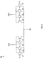
- FIG 9 shows an example of the implementation of one segment of the differential switching circuitry 26 in Figure 5 .
- the circuitry 90 in the segment comprises 8 FETs S1 to S8 which, in this example, are all n-type devices.
- the FETs are arranged in first to fourth pairs, with each pair having a first FET connected between a first output node OUTA of the circuitry and a common node TAIL and a second FET connected between a second output node OUTB of the circuitry and the common node TAIL.
- Each of the FETs receives one of the drive signals V S1 to V S8 produced by the corresponding segment ( Figure 8 ) of the switch driver circuitry 22.
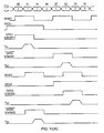
- the DAC operates in a repeating sequence of four phases. These phases are identified in the diagrams showing the complementary clock signals CLK and CLK in Figures 10(A) and 10(B) .
- the first mask signal MASK 1 changes to the high level near to the beginning of that phase 4. This change is triggered by the rising edge in BCLK. This causes the mask signals MASK 1 and MASK 3 to change state, as described previously with reference to Figure 7 .
- the precise timing at which the mask signal MASK 1 changes to the high level is not critical. All that matters is that MASK 1 changes to the high level in advance of the next rising edge in CLK , for reasons that will become apparent.
- the data signal DATA 1 was changed from the low level to the high level (the timing is actually during the preceding phase 3).
- This change in the data signal DATA 1 denotes that in the coming phase 1, out of the transistors S1 and S2 in the first pair, the transistor S1 should be turned on and the other transistor S2 should be turned off.
- the driver circuit 40 1 receives the data signal DATA 1 and the mask signal MASK 1.
- the clock switch 62 is turned on (it was previously off) and the other switch 64 is turned off (it was previously on).
- the clock signal LCLK has substantially the same potential as the potential V LO , so changing the states of the switches 62 and 64 during phase 4 does not affect the drive signal V S1 which remains at V LO .
- the timing of the rising edge in the drive signal V S1 is controlled exclusively by the clock signal LCLK , and not by the timing of the mask signal MASK 1 or the timing of the data signal DATA 1. Accordingly, even if there is jitter in MASK 1 and DATA 1 this will not affect the operation of the circuitry.
- the switch S1 is turned off at the end of phase 1 by the falling edge of LCLK .
- the mask signal MASK 1 must remain at the high level until at least after that falling edge. Accordingly, again, the timing of the falling edge in V S1 is determined exclusively by the clock signal LCLK and is uninfluenced by the mask signal MASK 1 or the data signal DATA 1.
- phase 2 the switch S4 is turned on.
- the data signal DATA 2 which causes this to happen is set at a time when the related mask signal MASK 2 is at the low level, for example some time during the preceding phase 4. In this case, the data signal DATA 2 is unchanged and remains at the low level. Accordingly, the clock switch 62 in the driver portion for V S3 remains off (the other switch 64 remains on) and the clock switch 72 in the driver portion for V S4 remains on (the other switch 74 remaining off). Thus, V S3 remains at V LO in phase 2 and V S4 rises with LCLK at the beginning of phase 2 and falls with LCLK at the end of phase 2.
- the process continues in the subsequent phases 3, 4, etc.
- the data signal DATA 3 is changed from high to low (around the beginning of the first "phase 1" shown in Figure 10(B) ).
- the clock switch 72 in the driver portion for V S6 is changed from off to on.
- the other switch 74 in that driver portion is changed from on to off. No change in the drive signal V S6 occurs until the rising edge of LCLK in phase 3.
- the drive signal V S6 then changes back to V LO at the end of phase 3, when the clock signal LCLK has its next falling edge.
- the other FET of the same pair, S5 is kept off because the data signal DATA 3 is low.
- phase 4 S7 is turned on.
- the data signal DATA 4 is changed from low to high during the preceding inactive period of the mask signal MASK 4 (around the beginning of the preceding phase 2).
- the clock switch 62 in the driver portion for the drive signal V S7 is turned on at the rising edge of MASK 4 (near to the beginning of phase 3).
- the other switch 64 in that driver portion is turned off at this time.
- the clock signal LCLK is delivered via the clock switch to the switch S7.
- the other FET of the same pair, S8, is maintained off in phase 4 because DATA4 is low.
- the mask signals are used to enable or disable the drive signals V S1 to V S8 for the FETs in the differential switching circuitry.
- these mask signals are not used to control the timing of the changes in the drive signals. The timing of those changes is determined by the timing of the complementary clock signals themselves.
- each active period of the mask signal begins before the relevant rising edge of the clock signal LCLK/ LCLK and ends after the falling edge of that clock signal. Jitter, if any, on the mask signals does not affect the timing of the changes in the drive signals.
- FIG 11 shows another example of the possible implementation of the switch controller in the mask generator circuit 38.
- a latch 100 has the data signal DATA 1 applied to its data input D.
- the mask signal MASK 1 is applied to its clock input CLK.
- the latch 100 is a so-called "strong-arm" latch and operates as follows.
- MASK 1 When MASK 1 is low, transistors 102 and 104 are ON, so that the outputs C1 and C3 of inverters 112 and 122 are both low and the outputs C2 and C4 of inverters 114 and 124 are both high.
- Transistor 101 is OFF.
- MASK 1 changes from low to high, transistor 101 turns ON. In this condition, if DATA 1 is high, transistor 106 will be ON and transistor 108 will be OFF, so that the input to inverter 122 goes low. This turns ON transistor 107 which forces the input of inverter 112 to go high.
- C1 stays low
- C2 stays high
- the output C1 DATA 1.MASK 1
- the output C2 DATA1.MASK1
- the output C3 DATA1 .MASK 1
- the output C4 DATA1 .MASK 1 as in Figure 8 .
- Figure 11 circuitry over the corresponding gate circuitry 80 in Figure 8 is that problems associated with different gates having different delays are avoided. Also, the latch outputs have a return-to-zero format which results in a constant supply current. This gives the further advantage that the supply current is independent of the data signals. This may make it possible to use the power supply for the analog circuits to power the latches, too.
- the embodiment described above operates in four phases, it will be appreciated that the number of phases is not limited to four. Three phases could be used, or five or more phases could be used. In general, the more phases that are used, the greater the interval between successive active periods of the mask signals. This gives more time to change the data signals during these inactive periods. However, the more phases that are used, the greater the number of FETs in the differential switching circuitry and hence the more parasitic capacitances associated with those FETs. This can mean that the circuitry will operate less fast. The use of four phases therefore seems a good compromise for operation at 12 G samples/s.
- the present invention is also applicable in other situations in which it is desirable to generate carefully controlled drive signals for a plurality of different switchable elements (e.g. FETs).
- the present invention is applicable in high-speed input/output circuits.
- a plurality of circuitry portions may need to be connected to the same input or output node.
- a plurality of switchable elements may be provided between the input or output node and the circuitry portions. These switchable elements can be controlled by switch driver circuitry embodying the present invention.
Description
- The present invention relates to switching circuitry for use, for example, in high-speed digital-to-analog converters (DACs).
-
Figure 1 shows an overview of a previously considered DAC. The DAC inFigure 1 is part of a DAC integrated circuit (IC) of the current-steering type, and is designed to convert an m-bit digital input word (D1-Dm) into a corresponding analog output signal. - Referring to
Figure 1 , theDAC 1 contains analog circuitry including a number n of identicalcurrent sources 21 to 2n, where n = 2m-1. Eachcurrent source 2 passes a substantially constant current I. The analog circuitry further includes a number n ofdifferential switching circuits 41 to 4n corresponding respectively to the ncurrent sources 21 to 2n. Eachdifferential switching circuit 4 is connected to its correspondingcurrent source 2 and switches the current I produced by the current source either to a first terminal, connected to a first connection line A of the converter, or a second terminal connected to a second connection line B of the converter. - Each
differential switching circuit 4 receives one of a plurality of digital control signals T1 to Tn (called "thermometer-coded signals" for reasons explained hereinafter) and selects either its first terminal or its second terminal in accordance with the value of the signal concerned. A first output current IA of theDAC 1 is the sum of the respective currents delivered to the first terminals of the differential switching circuit, and a second output current IB of theDAC 1 is the sum of the respective currents delivered to the second terminals of the differential switching circuit. The analog output signal is the voltage difference VA-VB between a voltage VA produced by sinking the first output current IA of theDAC 1 into a resistance R and a voltage VB produced by sinking the second output current IB of the converter into another resistance R. - The thermometer-coded signals T1 to Tn are derived from the binary input word D1-Dm by digital circuitry including a binary-
thermometer decoder 6. Thedecoder 6 operates as follows. When the binary input word D1-Dm has the lowest value the thermometer-coded signals T1-Tn are such that each of thedifferential switching circuits 41 to 4n selects its second terminal so that all of thecurrent sources 21 to 2n are connected to the second connection line B. In this state, VA=0 and VB=nIR. The analog output signal VA-VB=-nIR. As the binary input word D1-Dm increases progressively in value, the thermometer-coded signals T1 to Tn produced by thedecoder 6 are such that more of the differential switching circuits select their respective first terminals (starting from the differential switching circuit 41) without any differential switching circuit that has already selected its first terminal switching back to its second terminal. When the binary input word D1-Dm has the value i, the first idifferential switching circuits 41 to 4i select their respective first terminals, whereas the remaining n-idifferential switching circuits 4i+1 to 4n select their respective second terminals. The analog output signal VA-VB is equal to (2i-n)IR. - Thermometer coding is popular in DACs of the current-steering type because, as the binary input word increases, more current sources are switched to the first connection line A without any current source that is already switched to that line A being switched to the other line B. Accordingly, the input/output characteristic of the DAC is monotonic and the glitch impulse resulting from a change of 1 in the input word is small.
- An exemplary differential switching circuit suitable for use with the DAC of
Figure 1 is shown inFigure 2 . This differential switching circuit comprises first and second PMOS field-effect transistors (FETs) S1 and S2. The respective sources of the transistors S1 and S2 are connected to a common node TAIL to which a corresponding current source (21 to 2n inFigure 1 ) is connected. The respective drains of the transistors S1 and S2 are connected to respective first and second output nodes OUTA and OUTB of the circuit which correspond respectively to the first and second terminals of each of the differential switching circuits shown inFigure 1 . - Each transistor S1 and S2 has a
corresponding driver circuit driver circuits Figure 2 , when the input signal IN has the high level (H) and the input signal INB has the low level (L), the switching signal SW1 (gate drive voltage) for the transistor S1 is at the low level L, causing that transistor to be ON, whereas the switching signal SW2 (gate drive voltage) for the transistor S2 is at the high level H, causing that transistor to be OFF. Thus, in this condition, all of the input current flowing into the common node TAIL is passed to the output node OUTA and no current passes to the output node OUTB. - When it is desired to change the state of the circuit of
Figure 2 so that the transistor S1 is OFF and the transistor S2 is ON, complementary changes are made simultaneously in the input signals IN and INB such that the input signal IN changes from H to L at the same time as the input signal INB changes from L to H. As a result of these complementary changes the transistor S1 turns OFF and the transistor S2 turns ON, so that all of the input current flowing into the common node TAIL is passed to the output node OUTB and no current passes to the output node OUTA. - One problem with the DAC of
Figure 1 is third-order distortion. Third order distortion is particularly undesirable in DACs which produce multi-tone output signals, since third order intermodulation distortion may occur in-band, in which case it cannot be removed by filtering. Such third order distortion is believed to be due in part to currents flowing into and out of parasitic capacitances which are present in the differential switching circuits (Figure 2 ). - To address this problem, and other problems associated with the DAC of
Figures 1 and 2 , the present applicants have proposed inEP-A-1720258 a modified differential switching circuit as shown inFigure 3 . Thisdifferential switching circuit 10 differs from the differential switching circuit ofFigure 2 in that it has two FETs associated with each output node OUTA and OUTB. In particular, the first and third FETs S1 and S3 are connected between a first output node OUTA and a common node TAIL. The second and fourth FETs S2 and S4 are connected between a second output node OUTB and the common node TAIL. Each of these four FETs S1 to S4 is turned on or off by a drive signal VS1 to VS4 applied thereto. - The
differential switching circuit 10 ofFigure 3 is designed to operate in alternating first and second phases, which may be referred to odd and even phases. The first and second FETs S1 and S2 constitute a first pair of FETs which are available in each odd phase. The third and fourth FETs S3 and S4 constitute a second pair of FETs which are available in each even phase. In each odd phase, one of the FETs of the pair S1 and S2 is turned on and the other of those FETs is turned off. Both transistors of the second pair (S3 and S4) are off. In each even phase, one FET of the pair S3 and S4 is turned on and the other is turned off. The two FETs of the first pair S1 and S2 are both off. The FET which is turned on in a pair is determined by the data applied to the DAC, as will be explained later. - The advantage of the
Figure 3 differential switching circuit 10 is that at the start of each odd or even phase the same number of FETs change state. One FET will always be turning on and another FET will always be turning off. For example, consider the case in which S1 is on in an odd phase and then in the next even phase the data remains unchanged. In that case, at the start of the even phase concerned, S1 turns off and S3 turns on, S2 and S4 remaining off. In theFigure 2 differential switch circuit, this is not possible, the switch S1 simply remaining on in successive cycles when the data is unchanged. This means that in theFigure 2 circuit, the number of FETs that change state from one cycle to the next is dependent on the data. In theFigure 3 circuit, on the other hand, the number of FETs that change state from one phase to the next is independent of the data. By arranging the same number of FETs to change state in each phase, the charge which flows into and out of the parasitic capacitances in the circuitry is less dependent on the input data signal. This helps to reduce third order distortion which may occur in the analog output signal. - There are other advantages associated with the
Figure 3 circuitry, too. In particular, by arranging the same number of FETs to change state in each phase, the current drawn by each analog segment is approximately the same in each phase. This should help to reduce variations in the timings of the switching operations of the different analog segments, which again may lead to reduced distortion. - Another problem which exists in the DAC of
Figures 1 and 2 is timing mis-matches between different analog segments and between different switching parts of the same segment. For example, in theFigure 2 circuit problems will arise if the signals IN and INB applied to one analog segment change at times different from the corresponding signals in other analog segments. Furthermore, even if it could be ensured that there is no timing variation between the IN and INB signals of different analog segments, a problem still arises if the twodifferent switch drivers drivers - To address the timing mismatch problem, the present applicant has proposed in
EP-A-1720258 modified switch driver circuitry as shown inFigure 4 . This modifiedswitch driver circuitry 12 is connected to thedifferential switch circuit 10 ofFigure 3 , and supplies the drive signals VS1 to VS4 FETs S1 to S4 in thedifferential switching circuit 10. - The
Figure 3 switch driver circuitry comprises first andsecond circuits circuit Figure 3 . For example, in the case of thefirst circuit 14, the first output node is connected to the gate of S1 of the first pair of FETs and the second output node is connected to the gate of S2 in the first pair. The first output node of thesecond circuit 16 is connected to the gate of S3 in the second pair of FETs S3 and S4, and the second output node of thesecond circuit 16 is connected to the gate of S4. Each of the first andsecond circuits - Each of the first and
second circuits first circuit 14 the complementary data signals are the signals TODD andT ODD. In the case of thesecond circuit 16 the complementary data signals are the signals TEVEN andT EVEN. The complementary data signals TODD andT ODD for thefirst circuit 14 are generated by a first decoder of the DAC. The complementary data signals TEVEN andT EVEN for thesecond circuit 16 are generated by a second decoder, separate from the first decoder. Each of these decoders carries out a binary-thermometer decoding operation. The frequency of the decoding operations performed by each decoder need only be half the frequency of the conversion cycles of the DAC. This can be useful for reducing power consumption of the decoding circuitry. It may also be useful where the DAC conversion frequency is so high that carrying out decoding operations at the DAC conversion frequency using a single decoder is problematic. - Each of the first and
second circuits first circuit 14 are both controlled by the inverted data signalT ODD. The switches SW5 and SW8 in thefirst circuit 14 are both controlled by the data signal TODD. The switches SW2 and SW3 in thesecond circuit 16 are both controlled by the inverted data signalT EVEN. The switches SW1 and SW4 in thesecond circuit 16 are both controlled by the data signal TEVEN. - In operation of the
Figure 4 switch driver circuitry, the clock signal CLKODD is active (low) and the clock signal CLKEVEN is inactive (high) in each odd phase. The clock signals CLKODD and CLKEVEN are inactive (high) and active (low) in each even-numbered phase. Any changes to the data signals applied to eithercircuit T ODD are made only in even phases when CLKODD is inactive (high). Similarly, any changes in the data signals TEVEN andT EVEN are made only in odd phases, i.e. when CLKEVEN is inactive (high). - When the clock signal applied to the first or second circuit is inactive (high) any changes in the data signals applied to the circuit concerned have no effect on the output node potentials. For example, consider the case of the
first circuit 14 when a change is made to the data signals during an even phase. Assume that initially SW5 and SW8 are on and SW6 and SW7 are off. The drive signal VS1 at the first output node will be equal to the high potential of CLKODD (this potential is deliberately made to be the same as VDD). The drive signal VS2 at the second output node will be VDD. In this condition, S1 and S2 inFigure 3 are both off. If the data signals are now changed, SW5 and SW8 turn off and SW6 and SW7 turn on. The drive signals VS1 and VS2 remain substantially unchanged (VDD and the high potential of CLKODD respectively). - At the start of each odd phase, CLKODD undergoes an activating change, that is it changes from high to low. At this time, depending on the data signals in the preceding even phase, one of the two switches SW7 and SW8 will already have been turned on, and the other of those two switches will already have been turned off. This means that the change in the clock signal CLKODD is transmitted via the on switch to the relevant output node without having to turn on the switch concerned. In other words, the switch is turned on in advance of the activating change in the clock signal. Accordingly, the activating change in the clock signal is delivered to the required output node with as small a delay as possible. This means that the inputs to the gates of the FETs in the
differential switch circuit 10 ofFigure 3 change as quickly as possible. Although it is still possible for there to be delay mismatch between, for example, the switches SW7 and SW8, this mismatch should be small because the delays imposed by the switches themselves are small. - Accordingly, the
switch driver circuitry 12 inFigure 4 is effective in reducing the effect of switching delay mismatches. However, the present applicants are now contemplating a DAC capable of operating at a much higher conversion frequency, for example up to 12 Gsamples/s. This imposes some severe requirements on the circuitry. One way of relaxing these requirements is to increase the number of phases beyond two. This enables the decoders to have longer to carry out their decoding operations. For example, it might be contemplated to provide four pairs of switches in the differential switching circuit, instead of the two pairs shown inFigure 3 , and four circuits in the switch driver circuitry ofFigure 4 , instead of the twocircuits - However, in order to increase the number of individual circuits in the
switch driver circuitry 12 ofFigure 4 , it would be necessary to increase the number of clock signals from 2 to 4 as well. These four clock signals would need to be 90° out of phase with one another. Generating and delivering such multiphase clock signals to all of the different segments would be very difficult to do in practice. In the switch driver circuitry, the clock signals are used directly to provide the drive signals to the FETs in the differential switching circuitry. It follows that any timing errors in the clock signals will affect the performance of the differential switching circuitry directly. - It is therefore desirable to provide switch driver circuitry capable of multiphase operation without timing errors affecting the drive signals produced by the circuitry.
- According to a first aspect of the present invention there is provided switch driver circuitry as defined in
independent claim 1, to which the reader should now refer. Optional features are defined in the dependent claims. - Each said driver circuit may also comprise means for maintaining said output node at a predetermined potential when the clock switch is off, said predetermined potential preferably being substantially equal to the potential of the clock signal received at said clock input node prior to said preselected change.
- The maintaining means may comprise a further switch connected between said output node and a source of said predetermined potential, said switch controller preferably being operable to turn on said further switch when said clock switch is turned off.
- Preferably, the driver circuit also has a data input node at which a data signal is received, and the switch controller is preferably operable to employ the data signal to determine whether or not to turn on the clock switch during said active period of the received mask signal.
- Each said driver circuit may have first and second output nodes and first and second clock switches, said first clock switch being connected between said clock input node and said first output node and said second clock switch being connected between said clock input node and said second output node, and the switch controller may be operable to select one of the first and second clock switches in dependence upon said data signal and to turn on the selected clock switch in advance of said preselected change.
- The switch controller may comprise a latch connected for receiving said data signal and a signal complementary thereto and also connected for receiving said mask signal, the latch having a first output connected to a control terminal of said first clock switch and a second output connected to a control terminal of said second clock switch, the latch being arranged so that during said inactive period of the mask signal the first and second outputs are both in an OFF state, in which the first and second clock signals are off and so that, at the start of each active period of the mask signal, one of the first and second outputs changes from an OFF state to an ON state, in which said one clock switch is turned ON, and the other of the two outputs remains in the OFF state, the first and second outputs remaining unchanged if the data input changes subsequently during the active period concerned.
- The mask generator circuit may be operable to cause said active period of the mask signal received by each said driver circuit to begin prior to a first preselected change in the clock signal received at the clock input node of the driver circuit concerned and to end after a second preselected change in that clock signal.
- The first and second preselected changes may be successive edges of the clock signal concerned, one of the edges being a rising edge and the other of the edges being a falling edge.
- Any changes in the data signal at the data input node of one of the driver circuits may be made during an inactive period of the mask signal received at the mask input node of the driver circuit concerned.
- The circuitry may further comprise means for adjusting a duty cycle of said one or more clock signals applied to the mask generating circuit.
- According to an embodiment of a second aspect of the present invention there is provided switching circuitry comprising: switch driver circuitry according to the aforementioned first aspect of the present invention; and a switching circuit having a plurality of switchable elements, each connected to one of the said output nodes of the switch driver circuitry for receiving respective drive signals therefrom.
- The switching circuit may be a differential switching circuit having a common node and first and second switch nodes, the plurality of switchable elements being operable to connect the common node to a selected one of the first and second switch nodes in each of said phases. Preferably, the number of switchable elements which change state from one phase to the next is constant.
- According to an embodiment of a third aspect of the present invention there is provided a digital-to-analog converter comprising switching circuitry according to the aforementioned second aspect of the present invention.
- It will be appreciated that method aspects (although not directly embodying the invention claimed) may be provided corresponding respectively to the above three aspects of the present invention. It will further be appreciated that features of the aforementioned first to third aspects of the present invention apply to such methods and vice versa.
- According to an embodiment of a fourth aspect of the present invention, there is provided an IC chip or chipset comprising switch driver circuitry according to the aforementioned first aspect of the present invention, or comprising switching circuitry according to the aforementioned second aspect of the present invention, or comprising a digital-to-analog converter according to the aforementioned third aspect of the present invention.
- According to an embodiment of a fifth aspect of the present invention, there is provided a circuit board comprising switch driver circuitry according to the aforementioned first aspect of the present invention, or comprising switching circuitry according to the aforementioned second aspect of the present invention, or comprising a digital-to-analog converter according to the aforementioned third aspect of the present invention.
- According to an embodiment of a sixth aspect of the present invention, there is provided an RF transmitter comprising a digital-to-analogue converter according to the aforementioned third aspect of the present invention. Such an RF transmitter may be part of a base station, relay station or a mobile device, and accordingly the present invention extends to this equipment too.
- Reference will now be made, by way of example, to the accompanying drawings, in which:
-
Figure 1 , discussed hereinbefore, shows parts of a previously-considered DAC; -
Figure 2 , also discussed hereinbefore, shows parts of differential switching circuitry previously considered for use in theFigure 1 DAC; -
Figure 3 another example of differential switching circuitry previously considered suitable for use in theFigure 1 DAC; -
Figure 4 shows parts of switch driver circuitry previously considered for use in a DAC; -
Figure 5 shows parts of a DAC embodying the present invention; -
Figure 6 shows switch driver circuitry according to an embodiment of the present invention; -
Figure 7 shows one of the parts of the switch driver circuitry ofFigure 6 ; -
Figure 8 shows another of the parts of theFigure 6 switch driver circuitry; -
Figure 9 shows differential switching circuitry suitable for use with theFigure 6 switch driver circuitry; -
Figures 10(A) and10(B) show waveforms generated by theFigure 6 switch driver circuitry in operation; and -
Figure 11 shows one part of switch driver circuitry according to another embodiment of the present invention. -
Figure 5 shows parts of a DAC embodying the present invention. The DAC is intended to have a conversion frequency of up to 12 G samples/s. Such a DAC may be used, for example, to synthesise a radio-frequency (RF) signal in a mobile telephone base station. The DAC is segmented and has a plurality of analog segments in the same basic manner as the DAC ofFigure 1 . - The parts of the DAC shown in
Figure 5 are mainly parts of the analog circuitry of the DAC. The DAC also comprises digital circuitry that is not shown inFigure 5 . This digital circuitry, for example, includes an array of decoders (for example 16 decoders), each of which carries out binary-to-thermometer decoding operations. With 16 decoders and a DAC conversion frequency of 12 G samples/s, each individual decoder is required to perform 750 million decoding operations per second. - The DAC analog circuitry comprises four multiplexer/retiming circuits 201 to 204. Each of these multiplexer/retiming circuits 201 to 204 receives the decoded data signals produced by four of the decoders of the decoder array. Each multiplexer/retiming circuit performs time-division multiplexing on the decoded data signals received from its four decoders to produce a stream of multiplexed data signals. The data signals are of the complementary type, and also there is one pair of complementary data signals per analog segment. For simplicity in
Figure 5 , only one such pair of complementary data signals is shown. Thus, the complementary data signals produced by the multiplexer/retiming circuit it 201 are thesignals DATA 1 andDATA1 , the complementary data signals produced by the multiplexer/retiming circuit 202 are thesignals DATA 2 andDATA2 , the complementary data signals produced by the multilplexer/retiming circuit 203 are thesignals DATA 3 andDATA3 , and the complementary data signals produced by the multiplexer/retiming circuit 204 are thesignals DATA 4 andDATA4 . Changes in each of these pairs of complementary data signals occur at a frequency of 3 GHz. - The four pairs of complementary data signals are supplied from the multiplexer/retiming circuits 201 to 204 to switch
driver circuitry 22. Theswitch driver circuitry 22 also receives a pair of complementary clock signals CLK andCLK from aclock circuit 24. The frequency of each of the clock signals CLK andCLK is 6 GHz. - The
switch driver circuitry 22 is segmented into n segments. Each of the segments receives the four pairs of complementary data signals (DATA 1 toDATA 4 andDATA1 toDATA4 ). Each segment derives from the received complementary data-signal parts and the complementary clock signals CLK andCLK a set of 8 drive signals VS1 to VS8. - The analog circuitry in
Figure 5 further comprisesdifferential switching circuitry 26 which is also segmented into n segments. Each segment of the differential switching circuitry receives the 8 drive signals VS1 to VS8 produced by the corresponding segment of theswitch driver circuitry 22 and produces an analog output signal for its segments. The respective analog output signals of the n segments of thedifferential switching circuitry 26 are then combined together to produce an analog output signal for the DAC. In this example, changes in the analog output signal can occur at 12 GHz. -
Figure 6 shows the circuitry in one segment of theswitch driver circuitry 22 ofFigure 5 . Thesegment 30 comprises abuffer 32, a level shift andedge control circuit 34, a dutycycle compensation circuit 36, amask generator circuit 38 and first to fourth driver circuits 401 to 404. - The
buffer 32 receives the pair of complementary clock signals CLK andCLK from theclock circuit 24 inFigure 5 . Thebuffer 32 amplifies the received clock signals and supplies buffered complementary clock signals BCLK andBCLK to the level shift andedge control circuit 34.Circuit 34 adjusts the voltage levels and edge timings of the complementary clock signals as necessary and supplies the resulting adjusted clock signals LCLK andLCLK to the driver circuits 401 to 404. - The duty
cycle compensation circuit 36 is connected to the inputs of thebuffer 32 and the outputs of the level shift andedge control circuit 34. The dutycycle compensation circuit 36 adjusts the duty cycle of the clock signals so that the adjusted clock signals LCLK andLCLK supplied to the driver circuits 401 and 404 have a 50% duty cycle. - For example, the clock signals CLK and
CLK may be generated off-chip and AC-coupled onto the chip. The clock paths for CLK andCLK may have an on-chip centre-tapped termination resistor. The duty cycle compensation circuit may then operate to adjust the common-node voltage of the clock signals CLK andCLK . This can be achieved by adding a voltage difference to the differential clock signals, for example by adjusting the equivalent termination voltages of the differential clock signals. This effectively moves the crossover point of the two waveforms (the rising/falling crossover is adjusted one way, and the falling/rising crossover is adjusted the other way), which adjusts the duty cycle. The adjustment can be carried out in many different ways. For example, it is possible to move each actual termination voltage (these being driven from the amplifiers). It is also possible to add to a differential current at the termination resistors. It is also possible to use "split" termination resistors with slightly more than an intended impedance to the centre tap and much higher impedance to an amplifier output which provides a DC offset. For example, when the intended impedance is 50Ω, the split resistors may be 55Ω and 500Ω. These possibilities are all equivalent to adding an input offset voltage to the differential clock signal to move the crossovers in opposite directions. The clock signals CLK andCLK may be approximately sinusoidal at the intended operating frequencies. - It would also be possible to connect the duty
cycle compensation circuit 36 to circuitry within thebuffer 32 to adjust the output skew rates of the buffer. - The buffered clock signals BCLK and
BCLK produced by thebuffer 32 are also applied to themask generator circuit 38. The mask generator circuit derives first to fourth mask signalsMASK 1,MASK 2,MASK 3 andMASK 4 from the buffered clock signals and supplies them respectively to the first to fourth driver circuits 401 to 404. The mask signals each have a frequency of half the frequency of the clock signals CLK andCLK . The different mask signals are 90° out of phase with one another. -
Figure 7 shows one example implementation of themask generator 38 inFigure 6 . Themask generator 38 comprises first and second flip-flops Q output connected to its D input. Accordingly, each flip-flop operates as a divide-by-two circuit. The first flip-flop 50 receives at its clock input the buffered clock signal BCLK. This flip-flop generates at its Q output the firstmask signal MASK 1 and generates at itsQ output the thirdmask signal MASK 3. Accordingly, at each rising edge of BCLK theoutputs MASK 1 andMASK 3 change state. Similarly, in the case of the second flip-flop 52, the second and fourth mask signalsMASK 2 andMASK 4 change state at each rising edge ofBCLK . Because the mask signals are generated using divide-by-two circuits, they each have a 50% duty cycle, without requiring any additional duty cycle correction circuitry. - Coming back to
Figure 6 , each of the four driver circuits 401 to 404 receives the pair of complementary decoded data signals for the segment concerned. Each driver circuit also receives one of the four mask signals MASK 1 toMASK 4. Each of the driver circuits 401 to 404 produces two of the eight drive signals. The driver circuit 401 produces the drive signals VS1 and VS2, the driver circuit 402 produces the drive signals VS3 and VS4, the driver circuit 403 produces the drive signals VS5 and VS6, and the driver circuit 404 produces the drive signals VS7 and VS8. -
Figure 8 shows an example implementation of the first driver circuit 401. The driver circuit 401 in this example has afirst driver portion 60 and asecond driver portion 70. The driver circuit 401 also comprises aswitch controller 80. - The
first driver portion 60 is used to provide the drive signal VS1. Thefirst driver portion 60 comprises a switch 62 (hereinafter a "clock switch") connected between a clock input node of thefirst driver portion 60 and an output node of the driver portion. The adjusted clock signalLCLK is received at the clock input node. Theclock switch 62 is controlled by a first control signal C1 generated by theswitch controller 80. Theswitch controller 80 comprises an ANDgate 82 which receives at its inputs the data signalDATA 1 and themask signal MASK 1. Thus, C1=DATA 1.MASK 1. - The first
switch driver portion 60 further comprises a switch 64 connected between the output node and a node of the driver portion which is maintained at a predetermined low potential VLO. This low potential VLO is maintained at substantially the same potential as the potential of each of the adjusted clock signals LCLK andLCLK when in the low (inactive) state. Theswitch controller 80 comprises aNAND gate 84 which, similarly to the ANDgate 82, receives thesignals DATA 1 andMASK 1 at its inputs. The output signal C2 of theNAND gate 84 is thereforeDATA 1. MASK 1 . - The second
switch driver portion 70 provides the drive signal VS2. Thissecond driver portion 70 has a clock input node at which the clock signalLCLK is received. Aclock switch 72 is arranged between the clock input node and the output node of thesecond driver portion 70. Thisswitch 72 is controlled by a control signal C3 produced by theswitch controller 80. Theswitch controller 80 comprises an ANDgate 86 which receives at its inputs the inverted data signalDATA1 and themask signal MASK 1. Thus C3=DATA1 .MASK 1. - The second
switch driver portion 70 further comprises a switch 74 connected between the output node and the node having the potential VLO. This switch is controlled by a control signal C4 produced by aNAND gate 88 in theswitch controller 80. The inputs to theNAND gate 88 are the same as the inputs to the ANDgate 86 so that C4=DATA 1+MASK1 . - The other driver circuits 402 to 404 are implemented in basically the same manner as the first driver circuit 401. Table 1 below shows any differences in the connection arrangements. Each row in
column 1 corresponds to one of the two switch driver portions in a driver circuit. For example, the entries for the third row (VS3) show that the driver portion used to generate the drive signal VS3 has LCLK connected to its clock input node, DATA 2.MASK 2 applied to its clock switch andDATA 2. applied to its other switch.MASK 2Table 1 Clock input node Clock switch Other switch VS1 LCLK DATA 1. MASK 1DATA1.MASK 1VS2 LCLK DATA1.MASK1 DATA1+ MASK1 VS3 LCLK DATA 2. MASK 2DATA2.MASK2 VS4 LCLK DATA 1. MASK 1DATA2+ MASK1 VS5 LCLK DATA 3. MASK 3DATA 3.MASK 3 VS6 LCLK DATA3.MASK3 DATA3+MASK3 VS7 LCLK DATA 4. MASK 4DATA4.MASK4 VS8 LCLK DATA4.MASK DATA 4+MASK4 -
Figure 9 shows an example of the implementation of one segment of thedifferential switching circuitry 26 inFigure 5 . Thecircuitry 90 in the segment comprises 8 FETs S1 to S8 which, in this example, are all n-type devices. The FETs are arranged in first to fourth pairs, with each pair having a first FET connected between a first output node OUTA of the circuitry and a common node TAIL and a second FET connected between a second output node OUTB of the circuitry and the common node TAIL. - Each of the FETs receives one of the drive signals VS1 to VS8 produced by the corresponding segment (
Figure 8 ) of theswitch driver circuitry 22. - Operation of the DAC of
Figures 5 to 9 will now be described with reference to the timing diagrams ofFigures 10(A) and10(B) . - As shown in the timing diagrams, the DAC operates in a repeating sequence of four phases. These phases are identified in the diagrams showing the complementary clock signals CLK and
CLK inFigures 10(A) and10(B) . - It is assumed that, in the first phase labelled "4" in the figures, the FET S8 in
Figure 9 is on and all of the other FETs S1 to S7 are off. The firstmask signal MASK 1 changes to the high level near to the beginning of thatphase 4. This change is triggered by the rising edge in BCLK. This causes the mask signalsMASK 1 andMASK 3 to change state, as described previously with reference toFigure 7 . The precise timing at which themask signal MASK 1 changes to the high level is not critical. All that matters is thatMASK 1 changes to the high level in advance of the next rising edge inCLK , for reasons that will become apparent. - As can be seen from
Figure 10(A) , at a time before the rising edge ofMASK 1, the data signalDATA 1 was changed from the low level to the high level (the timing is actually during the preceding phase 3). This change in the data signalDATA 1 denotes that in the comingphase 1, out of the transistors S1 and S2 in the first pair, the transistor S1 should be turned on and the other transistor S2 should be turned off. The driver circuit 401 receives the data signalDATA 1 and themask signal MASK 1. When these signals are both high, i.e. at the rising edge ofMASK 1 inphase 4, theclock switch 62 is turned on (it was previously off) and the other switch 64 is turned off (it was previously on). Inphase 4 the clock signalLCLK has substantially the same potential as the potential VLO, so changing the states of theswitches 62 and 64 duringphase 4 does not affect the drive signal VS1 which remains at VLO. - However, as soon as
LCLK changes from low to high at the beginning ofphase 1, this change is passed via theclock switch 62 directly to the gate of the FET S1 so that the FET S1 is turned on at substantially the same time asLCLK rises. - It can therefore be seen that the timing of the rising edge in the drive signal VS1 is controlled exclusively by the clock signal
LCLK , and not by the timing of themask signal MASK 1 or the timing of the data signalDATA 1. Accordingly, even if there is jitter inMASK 1 andDATA 1 this will not affect the operation of the circuitry. - In the case of the drive signal VS2 for the FET S2, this remains fixed at VLO in
phase 1 becauseDATA1 is low inphase 1. Accordingly, the clock signalLCLK present at the clock input node of thesecond driver portion 70 inFigure 8 is not passed through to the output node thereof. - The switch S1 is turned off at the end of
phase 1 by the falling edge ofLCLK . For this reason, themask signal MASK 1 must remain at the high level until at least after that falling edge. Accordingly, again, the timing of the falling edge in VS1 is determined exclusively by the clock signalLCLK and is uninfluenced by themask signal MASK 1 or the data signalDATA 1. - In the next phase (phase 2) the switch S4 is turned on. The data signal
DATA 2 which causes this to happen is set at a time when the relatedmask signal MASK 2 is at the low level, for example some time during thepreceding phase 4. In this case, the data signalDATA 2 is unchanged and remains at the low level. Accordingly, theclock switch 62 in the driver portion for VS3 remains off (the other switch 64 remains on) and theclock switch 72 in the driver portion for VS4 remains on (the other switch 74 remaining off). Thus, VS3 remains at VLO inphase 2 and VS4 rises with LCLK at the beginning ofphase 2 and falls with LCLK at the end ofphase 2. - The process continues in the
subsequent phases mask signal MASK 3, the data signalDATA 3 is changed from high to low (around the beginning of the first "phase 1" shown inFigure 10(B) ). Accordingly, at the rising edge of theMASK 3 near to the beginning of the first "phase 2" inFigure 10(B) theclock switch 72 in the driver portion for VS6 is changed from off to on. At the same time, the other switch 74 in that driver portion is changed from on to off. No change in the drive signal VS6 occurs until the rising edge ofLCLK inphase 3. The drive signal VS6 then changes back to VLO at the end ofphase 3, when the clock signalLCLK has its next falling edge. Duringphase 3, the other FET of the same pair, S5, is kept off because the data signalDATA 3 is low. - In the
subsequent phase 4, S7 is turned on. The data signalDATA 4 is changed from low to high during the preceding inactive period of the mask signal MASK 4 (around the beginning of the preceding phase 2). Accordingly, theclock switch 62 in the driver portion for the drive signal VS7 is turned on at the rising edge of MASK 4 (near to the beginning of phase 3). The other switch 64 in that driver portion is turned off at this time. Accordingly, at the beginning ofphase 4, the clock signal LCLK is delivered via the clock switch to the switch S7. The other FET of the same pair, S8, is maintained off inphase 4 becauseDATA4 is low. - It can therefore be seen that in the DAC of
Figures 5 to 9 , the mask signals are used to enable or disable the drive signals VS1 to VS8 for the FETs in the differential switching circuitry. However, these mask signals are not used to control the timing of the changes in the drive signals. The timing of those changes is determined by the timing of the complementary clock signals themselves. - The generation of the four mask signals from the complementary clock signals is simple to achieve. Also, the timing of the changes in the mask signals is not especially critical. As mentioned above, all that matters is that each active period of the mask signal begins before the relevant rising edge of the clock signal LCLK/
LCLK and ends after the falling edge of that clock signal. Jitter, if any, on the mask signals does not affect the timing of the changes in the drive signals. - It will also be appreciated that the embodiment of
Figures 5 to 9 can operate using only a pair of complementary clock signals (the clock signals CLK andCLK ). It is therefore unnecessary to generate, and distribute over the chips, four clock signals that are out of phase with one another by 90°. -
Figure 11 shows another example of the possible implementation of the switch controller in themask generator circuit 38. Instead of using AND and NAND gates as in theswitch controller 80 shown inFigure 8 , it is possible to use latches. For example, alatch 100 has the data signalDATA 1 applied to its data input D. Themask signal MASK 1 is applied to its clock input CLK. - The
latch 100 is a so-called "strong-arm" latch and operates as follows. WhenMASK 1 is low,transistors 102 and 104 are ON, so that the outputs C1 and C3 ofinverters inverters Transistor 101 is OFF. WhenMASK 1 changes from low to high,transistor 101 turns ON. In this condition, ifDATA 1 is high,transistor 106 will be ON andtransistor 108 will be OFF, so that the input toinverter 122 goes low. This turns ONtransistor 107 which forces the input ofinverter 112 to go high. Thus, C1 stays low, C2 stays high, C3 becomes high and C4 becomes low. On the other hand, ifDATA 1 is low,transistor 108 will be ON andtransistor 106 will be OFF, so that the input toinverter 112 goes low. This turns ONtransistor 109 which forces the input ofinverter 122 to go high. Thus, C1 becomes high, C2 becomes low, C3 stays low and C4 stays high. - If
DATA 1 andDATA1 change whenMASK 1 is high, no change occurs in the output C1 to C4 becausetransistor 103 turns OFF in the event thattransistor 107 turned ON whenMASK 1 became high, and transistor 105 turns OFF in the event thattransistor 109 turned ON whenMASK 1 became high. - Thus, the output C1 = DATA 1.
MASK 1, the output C2 =DATA1.MASK1 , the output C3 =DATA1 .MASK 1, and the output C4 =DATA1 .MASK 1 as inFigure 8 . - Further latches of the same kind as shown in
Figure 11 can be used to generate the required control signals for the other switch driver circuits based on DATA 2-4.DATA2-4 and MASK 2-4. - One advantage of the
Figure 11 circuitry over thecorresponding gate circuitry 80 inFigure 8 is that problems associated with different gates having different delays are avoided. Also, the latch outputs have a return-to-zero format which results in a constant supply current. This gives the further advantage that the supply current is independent of the data signals. This may make it possible to use the power supply for the analog circuits to power the latches, too. - Although the embodiment described above operates in four phases, it will be appreciated that the number of phases is not limited to four. Three phases could be used, or five or more phases could be used. In general, the more phases that are used, the greater the interval between successive active periods of the mask signals. This gives more time to change the data signals during these inactive periods. However, the more phases that are used, the greater the number of FETs in the differential switching circuitry and hence the more parasitic capacitances associated with those FETs. This can mean that the circuitry will operate less fast. The use of four phases therefore seems a good compromise for operation at 12 G samples/s.
- The present invention is also applicable in other situations in which it is desirable to generate carefully controlled drive signals for a plurality of different switchable elements (e.g. FETs). For example, the present invention is applicable in high-speed input/output circuits. In such circuits, a plurality of circuitry portions may need to be connected to the same input or output node. In this case, a plurality of switchable elements may be provided between the input or output node and the circuitry portions. These switchable elements can be controlled by switch driver circuitry embodying the present invention.
- Although embodiments of the present invention have been described for use with differential switching circuitry, it is of course possible to use the invention in situations where there is no differential switching circuitry. For example, the invention could be applied to a single-ended multiplexer as well.
Claims (18)
- Switch driver circuitry (22) for driving a switching circuit (26), the circuitry being configured to operate in a repeating sequence of n phases, where n ≥ 3, and comprising:a mask generator circuit (38) connected for receiving one or more first clock signals and operable to derive therefrom a set of n mask signals which differ in phase one from the next by 360/n°; andn driver circuits (401 to 404), each having a mask input node at which a respective one of said n mask signals is received and a clock input node at which a second clock signal is received, that second clock signal being related in timing to said one or more first clock signals such that it has a preselected change of state during an active period of the received mask signal, and each said driver circuit also having a clock switch (62, 72) connected between its clock input node and an output node of that driver circuit and also having a switch controller (80) operable to employ the mask signal received at the mask input node of that driver circuit to turn on the clock switch of that driver circuit in advance of the preselected change of state of the second clock signal received at the clock input node of that driver circuit based on the active period of the mask signal received at the mask input node of that driver circuit so as to connect its clock input node to its output node.
- Circuitry as claimed in claim 1, wherein each said driver circuit also comprises means (80, 64, 74) for maintaining its output node at a predetermined potential when its clock switch is off, said predetermined potential being substantially equal to the potential of the second clock signal received at its clock input node prior to the preselected change of state concerned.
- Circuitry as claimed in claim 2, wherein each said maintaining means comprises a further switch (64, 74) connected between the output node of the driver circuit concerned and a source of said predetermined potential, the switch controller (80) of that driver circuit being operable to turn on that further switch (64, 74) when the clock switch of that driver circuit is turned off.
- Circuitry as claimed in any preceding claim, wherein:each said driver circuit also has a data input node at which a data signal is received; andfor each said driver circuit, the switch controller (80) is operable to employ the data signal concerned to determine whether or not to turn on the clock switch (62, 72) concerned during said active period of the respective received mask signal.
- Circuitry as claimed in claim 4, wherein:each said driver circuit has first and second output nodes and first and second clock switches (62 & 72), said first clock switch (62) being connected between said clock input node and said first output node and said second clock switch (72) being connected between said clock input node and said second output node; andfor each said driver circuit, the switch controller (80) is operable to select one of the first and second clock switches in dependence upon said data signal and to turn on the selected clock switch in advance of said preselected change of state.
- Circuitry as claimed in claim 5, wherein, for each said driver circuit, the switch controller comprises a latch connected for receiving said data signal and a signal complementary thereto and also connected for receiving said mask signal, the latch having a first output connected to a control terminal of said first clock switch and a second output connected to a control terminal of said second clock switch, the latch being arranged so that during said inactive period of the mask signal the first and second outputs are both in an OFF state, in which the first and second clock signals are off and so that, at the start of each active period of the mask signal, one of the first and second outputs changes from an OFF state to an ON state, in which said one clock switch is turned ON, and the other of the two outputs remains in the OFF state, the first and second outputs remaining unchanged if the data input changes subsequently during the active period concerned.
- Circuitry as claimed in any preceding claim, wherein said mask generator circuit (38) is operable to cause said active period of the mask signal received by each said driver circuit to begin prior to a first preselected change of state in the second clock signal received at the clock input node of the driver circuit concerned and to end after a second preselected change of state in that second clock signal.
- Circuitry as claimed in claim 7, wherein said first and second preselected changes of state are successive edges of the second clock signal concerned, one of the edges being a rising edge and the other of the edges being a falling edge.
- Circuitry as claimed in any of claims 5 to 8, wherein any changes in the data signal at the data input node of one of the driver circuits are made during an inactive period of the mask signal received at the mask input node of the driver circuit concerned.
- Circuitry as claimed in any preceding claim, further comprising means for adjusting a duty cycle of said one or more first clock signals applied to the mask generating circuit.
- Switching circuitry comprising:switch driver circuitry (22) as claimed in any preceding claim; anda switching circuit (26) having a plurality of switchable elements (51 to 58), each connected to one of the said output nodes of the switch driver circuitry for receiving respective drive signals therefrom.
- Switching circuitry as claimed in claim 11, wherein said switching circuit is a differential switching circuit having a common node and first and second switch nodes, the plurality of switchable elements (51 to 58) being operable to connect the common node to a selected one of the first and second switch nodes in each of said phases.
- Switching circuitry as claimed in claim 12, wherein the number of switchable elements which change state from one phase to the next is constant.
- A digital-to-analogue converter comprising switching circuitry as claimed in any of claims 11 to 13.
- An IC chip or chipset comprising switch driver circuitry as claimed in any of claims 1 to 10, or comprising switching circuitry as claimed in any of claims 11 to 13, or comprising a digital-to-analogue converter as claimed in claim 14.
- A circuit board comprising switch driver circuitry as claimed in any of claims 1 to 10, or comprising switching circuitry as claimed in any of claims 11 to 13, or comprising a digital-to-analogue converter as claimed in claim 14.
- An RF transmitter comprising a digital-to-analogue converter as claimed in claim 14.
- A base station, a relay station or a mobile device, comprising an RF transmitter as claimed in claim 17.
Priority Applications (1)
| Application Number | Priority Date | Filing Date | Title |
|---|---|---|---|
| EP20070113380 EP2019487B1 (en) | 2007-07-27 | 2007-07-27 | Switching circuitry |
Applications Claiming Priority (1)
| Application Number | Priority Date | Filing Date | Title |
|---|---|---|---|
| EP20070113380 EP2019487B1 (en) | 2007-07-27 | 2007-07-27 | Switching circuitry |
Publications (2)
| Publication Number | Publication Date |
|---|---|
| EP2019487A1 EP2019487A1 (en) | 2009-01-28 |
| EP2019487B1 true EP2019487B1 (en) | 2013-05-01 |
Family
ID=38805637
Family Applications (1)
| Application Number | Title | Priority Date | Filing Date |
|---|---|---|---|
| EP20070113380 Active EP2019487B1 (en) | 2007-07-27 | 2007-07-27 | Switching circuitry |
Country Status (1)
| Country | Link |
|---|---|
| EP (1) | EP2019487B1 (en) |
Cited By (8)
| Publication number | Priority date | Publication date | Assignee | Title |
|---|---|---|---|---|
| US8976050B1 (en) | 2013-09-12 | 2015-03-10 | Fujitsu Semiconductor Limited | Circuitry and methods for use in mixed-signal circuitry |
| US9054722B2 (en) | 2013-09-12 | 2015-06-09 | Fujitsu Semiconductor Limited | Circuitry and methods for use in mixed-signal circuitry |
| US9178523B2 (en) | 2013-09-12 | 2015-11-03 | Socionext Inc. | Circuitry and methods for use in mixed-signals circuitry |
| US9201813B2 (en) | 2013-09-12 | 2015-12-01 | Socionext Inc. | Signal distribution circuitry |
| US9344060B2 (en) | 2013-09-12 | 2016-05-17 | Socionext Inc. | Signal-alignment circuitry and methods |
| US9432013B2 (en) | 2013-09-12 | 2016-08-30 | Socionext Inc. | Circuitry useful for clock generation and distribution |
| US9450279B2 (en) | 2013-09-12 | 2016-09-20 | Socionext Inc. | Components and circuits for output termination |
| US9973186B2 (en) | 2013-09-12 | 2018-05-15 | Socionext Inc. | Circuitry and methods for use in mixed-signal circuitry |
Families Citing this family (2)
| Publication number | Priority date | Publication date | Assignee | Title |
|---|---|---|---|---|
| EP2019486B1 (en) | 2007-07-27 | 2014-12-10 | Fujitsu Semiconductor Limited | RF transmitters |
| US10644716B1 (en) | 2019-08-26 | 2020-05-05 | Analog Devices International Unlimited Company | Multi-path dual-switch digital-to-analog converter |
Family Cites Families (4)
| Publication number | Priority date | Publication date | Assignee | Title |
|---|---|---|---|---|
| JP3529883B2 (en) * | 1995-03-16 | 2004-05-24 | 株式会社東芝 | Signal converter |
| JP3420531B2 (en) * | 1999-06-07 | 2003-06-23 | 日本プレシジョン・サーキッツ株式会社 | Delta-sigma D / A converter |
| US6424283B2 (en) * | 2000-07-20 | 2002-07-23 | Texas Instruments Incorporated | Segmented high speed and high resolution digital-to-analog converter |
| GB2379107A (en) | 2001-08-24 | 2003-02-26 | Fujitsu Ltd | A DAC using clock-controlled current switches and exhibiting reduced dependence of errors on input data |
-
2007
- 2007-07-27 EP EP20070113380 patent/EP2019487B1/en active Active
Cited By (9)
| Publication number | Priority date | Publication date | Assignee | Title |
|---|---|---|---|---|
| US8976050B1 (en) | 2013-09-12 | 2015-03-10 | Fujitsu Semiconductor Limited | Circuitry and methods for use in mixed-signal circuitry |
| US9054722B2 (en) | 2013-09-12 | 2015-06-09 | Fujitsu Semiconductor Limited | Circuitry and methods for use in mixed-signal circuitry |
| US9178523B2 (en) | 2013-09-12 | 2015-11-03 | Socionext Inc. | Circuitry and methods for use in mixed-signals circuitry |
| US9201813B2 (en) | 2013-09-12 | 2015-12-01 | Socionext Inc. | Signal distribution circuitry |
| US9344060B2 (en) | 2013-09-12 | 2016-05-17 | Socionext Inc. | Signal-alignment circuitry and methods |
| US9432013B2 (en) | 2013-09-12 | 2016-08-30 | Socionext Inc. | Circuitry useful for clock generation and distribution |
| US9450279B2 (en) | 2013-09-12 | 2016-09-20 | Socionext Inc. | Components and circuits for output termination |
| US9705475B2 (en) | 2013-09-12 | 2017-07-11 | Socionext Inc. | Circuitry useful for clock generation and distribution |
| US9973186B2 (en) | 2013-09-12 | 2018-05-15 | Socionext Inc. | Circuitry and methods for use in mixed-signal circuitry |
Also Published As
| Publication number | Publication date |
|---|---|
| EP2019487A1 (en) | 2009-01-28 |
Similar Documents
| Publication | Publication Date | Title |
|---|---|---|
| EP2019487B1 (en) | Switching circuitry | |
| US7034733B2 (en) | Switching circuitry | |
| US7042379B2 (en) | Return-to-zero current switching digital-to-analog converter | |
| US8847806B2 (en) | Digital to analog converter comprising mixer | |
| CN104467862B (en) | Circuit and method in mixed signal circuit | |
| US6977602B1 (en) | Wide band digital to analog converters and methods, including converters with selectable impulse response | |
| WO2012176250A1 (en) | Differential switch drive circuit and current-steering d/a converter | |
| US8836559B2 (en) | Capacitive digital to analog converter | |
| CN106341134B (en) | Digital-to-analog converter with local interleaving and resampling | |
| US20060061499A1 (en) | High-speed and high-accuracy digital-to-analog converter | |
| Chang et al. | An 80-Gb/s 44-mW wireline PAM4 transmitter | |
| KR100698997B1 (en) | Data multiplexing in mixed-signal circuitry | |
| US20210234551A1 (en) | Current steering digital-to-analog conversion systems | |
| Khalil et al. | Toward millimeter-wave DACs: Challenges and opportunities | |
| US10771077B1 (en) | Hybrid return-to-zero voltage-mode DAC driver | |
| Balasubramanian et al. | Architectural trends in GHz speed DACs | |
| US8659458B1 (en) | Multiple return-to-zero current switching digital-to-analog converter for RF signal generation | |
| US9887552B2 (en) | Fine timing adjustment method | |
| EP3297168A1 (en) | Digital-to-analog converter circuit | |
| Kim et al. | A 12 bit 250 MS/s 28 mW+ 70 dB SFDR non-50% RZ DAC in 0.11 µm CMOS using controllable RZ window for wireless SoC integration | |
| US11394393B1 (en) | RF DAC with improved HD2 and cross-talk performance by shadow switching in bleeder path | |
| US20230362285A1 (en) | Multi-mode line driver circuit for the physical layer of a network connection, particularly of an ethernet communication, supporting different signal levels for different communication standards |
Legal Events
| Date | Code | Title | Description |
|---|---|---|---|
| PUAI | Public reference made under article 153(3) epc to a published international application that has entered the european phase |
Free format text: ORIGINAL CODE: 0009012 |
|
| AK | Designated contracting states |
Kind code of ref document: A1 Designated state(s): AT BE BG CH CY CZ DE DK EE ES FI FR GB GR HU IE IS IT LI LT LU LV MC MT NL PL PT RO SE SI SK TR |
|
| AX | Request for extension of the european patent |
Extension state: AL BA HR MK RS |
|
| 17P | Request for examination filed |
Effective date: 20090727 |
|
| AKX | Designation fees paid |
Designated state(s): DE FR GB |
|
| RAP1 | Party data changed (applicant data changed or rights of an application transferred) |
Owner name: FUJITSU MICROELECTRONICS LIMITED |
|
| RAP1 | Party data changed (applicant data changed or rights of an application transferred) |
Owner name: FUJITSU SEMICONDUCTOR LIMITED |
|
| 17Q | First examination report despatched |
Effective date: 20100608 |
|
| REG | Reference to a national code |
Ref country code: DE Ref legal event code: R079 Ref document number: 602007030133 Country of ref document: DE Free format text: PREVIOUS MAIN CLASS: H03K0017040000 Ipc: H03K0017160000 |
|
| GRAP | Despatch of communication of intention to grant a patent |
Free format text: ORIGINAL CODE: EPIDOSNIGR1 |
|
| RIC1 | Information provided on ipc code assigned before grant |
Ipc: H03M 1/06 20060101ALI20121016BHEP Ipc: H03K 17/16 20060101AFI20121016BHEP |
|
| GRAS | Grant fee paid |
Free format text: ORIGINAL CODE: EPIDOSNIGR3 |
|
| GRAA | (expected) grant |
Free format text: ORIGINAL CODE: 0009210 |
|
| AK | Designated contracting states |
Kind code of ref document: B1 Designated state(s): DE FR GB |
|
| REG | Reference to a national code |
Ref country code: GB Ref legal event code: FG4D |
|
| REG | Reference to a national code |
Ref country code: DE Ref legal event code: R096 Ref document number: 602007030133 Country of ref document: DE Effective date: 20130627 |
|
| PLBE | No opposition filed within time limit |
Free format text: ORIGINAL CODE: 0009261 |
|
| STAA | Information on the status of an ep patent application or granted ep patent |
Free format text: STATUS: NO OPPOSITION FILED WITHIN TIME LIMIT |
|
| 26N | No opposition filed |
Effective date: 20140204 |
|
| GBPC | Gb: european patent ceased through non-payment of renewal fee |
Effective date: 20130801 |
|
| REG | Reference to a national code |
Ref country code: FR Ref legal event code: ST Effective date: 20140331 |
|
| REG | Reference to a national code |
Ref country code: DE Ref legal event code: R097 Ref document number: 602007030133 Country of ref document: DE Effective date: 20140204 |
|
| PG25 | Lapsed in a contracting state [announced via postgrant information from national office to epo] |
Ref country code: FR Free format text: LAPSE BECAUSE OF NON-PAYMENT OF DUE FEES Effective date: 20130731 |
|
| PG25 | Lapsed in a contracting state [announced via postgrant information from national office to epo] |
Ref country code: GB Free format text: LAPSE BECAUSE OF NON-PAYMENT OF DUE FEES Effective date: 20130801 |
|
| REG | Reference to a national code |
Ref country code: DE Ref legal event code: R082 Ref document number: 602007030133 Country of ref document: DE Representative=s name: HOFFMANN - EITLE PATENT- UND RECHTSANWAELTE PA, DE |
|
| REG | Reference to a national code |
Ref country code: DE Ref legal event code: R081 Ref document number: 602007030133 Country of ref document: DE Owner name: SOCIONEXT INC., YOKOHAMA-SHI, JP Free format text: FORMER OWNER: FUJITSU SEMICONDUCTOR LIMITED, YOKOHAMA-SHI, KANAGAWA, JP Effective date: 20150512 Ref country code: DE Ref legal event code: R082 Ref document number: 602007030133 Country of ref document: DE Representative=s name: HOFFMANN - EITLE PATENT- UND RECHTSANWAELTE PA, DE Effective date: 20150512 |
|
| PGFP | Annual fee paid to national office [announced via postgrant information from national office to epo] |
Ref country code: DE Payment date: 20230719 Year of fee payment: 17 |