EP2009774A1 - Power converter, its control method, and air conditioner - Google Patents
Power converter, its control method, and air conditioner Download PDFInfo
- Publication number
- EP2009774A1 EP2009774A1 EP07741521A EP07741521A EP2009774A1 EP 2009774 A1 EP2009774 A1 EP 2009774A1 EP 07741521 A EP07741521 A EP 07741521A EP 07741521 A EP07741521 A EP 07741521A EP 2009774 A1 EP2009774 A1 EP 2009774A1
- Authority
- EP
- European Patent Office
- Prior art keywords
- power
- load
- current
- command value
- idc
- Prior art date
- Legal status (The legal status is an assumption and is not a legal conclusion. Google has not performed a legal analysis and makes no representation as to the accuracy of the status listed.)
- Granted
Links
Images



Classifications
-
- H—ELECTRICITY
- H02—GENERATION; CONVERSION OR DISTRIBUTION OF ELECTRIC POWER
- H02M—APPARATUS FOR CONVERSION BETWEEN AC AND AC, BETWEEN AC AND DC, OR BETWEEN DC AND DC, AND FOR USE WITH MAINS OR SIMILAR POWER SUPPLY SYSTEMS; CONVERSION OF DC OR AC INPUT POWER INTO SURGE OUTPUT POWER; CONTROL OR REGULATION THEREOF
- H02M5/00—Conversion of AC power input into AC power output, e.g. for change of voltage, for change of frequency, for change of number of phases
- H02M5/40—Conversion of AC power input into AC power output, e.g. for change of voltage, for change of frequency, for change of number of phases with intermediate conversion into DC
- H02M5/42—Conversion of AC power input into AC power output, e.g. for change of voltage, for change of frequency, for change of number of phases with intermediate conversion into DC by static converters
- H02M5/44—Conversion of AC power input into AC power output, e.g. for change of voltage, for change of frequency, for change of number of phases with intermediate conversion into DC by static converters using discharge tubes or semiconductor devices to convert the intermediate DC into AC
- H02M5/453—Conversion of AC power input into AC power output, e.g. for change of voltage, for change of frequency, for change of number of phases with intermediate conversion into DC by static converters using discharge tubes or semiconductor devices to convert the intermediate DC into AC using devices of a triode or transistor type requiring continuous application of a control signal
- H02M5/458—Conversion of AC power input into AC power output, e.g. for change of voltage, for change of frequency, for change of number of phases with intermediate conversion into DC by static converters using discharge tubes or semiconductor devices to convert the intermediate DC into AC using devices of a triode or transistor type requiring continuous application of a control signal using semiconductor devices only
-
- H—ELECTRICITY
- H02—GENERATION; CONVERSION OR DISTRIBUTION OF ELECTRIC POWER
- H02M—APPARATUS FOR CONVERSION BETWEEN AC AND AC, BETWEEN AC AND DC, OR BETWEEN DC AND DC, AND FOR USE WITH MAINS OR SIMILAR POWER SUPPLY SYSTEMS; CONVERSION OF DC OR AC INPUT POWER INTO SURGE OUTPUT POWER; CONTROL OR REGULATION THEREOF
- H02M1/00—Details of apparatus for conversion
- H02M1/12—Arrangements for reducing harmonics from AC input or output
Definitions
- the present invention relates to a power converter and its control method, and particularly to a power converter of a type commonly called “capacitor-less” and its control method.
- An air conditioner includes a motor for a refrigerant compressor, and a power converter for supplying desired power to the motor.
- a common power converter includes a converter, an inverter, and a smoothing capacitor between them, and converts power supplied from an alternating-current power supply.
- a reactor is provided to improve the input power factor. For example, the capacity of the reactor is about 2 mH, and the capacitance of the capacitor is about 2000 ⁇ F.
- the reactor and capacitor are especially large-sized and heavy-weighted among the parts of the power converter. Also, they constitute a cause of increased loss due to heat generation.
- Non-Patent Document 3 discloses a technique that further omits the reactor.
- Non-Patent Document 1 Myint Ko Tun and one other, "New Type Sinusoidal Input UPS Controlled by DC Chopper Type Active Filter", the Transactions III of Heisei 14 (2002 ) IEEJ Industry Applications Society Conference, The Institute of Electrical Engineers of Japan, August Heisei 14 (2002), pp. 1301-1306
- Non-Patent Document 2 Yoichi Ito and one other, "Capacitor-less PWM Inverter", The transactions of Showa 63 (1988 ) IEEJ Industry Applications Society National Conference, The Institute of Electrical Engineers of Japan, August Showa 63 (1988), pp.
- Non-Patent Document 3 Hitoshi Haga and one other, "Method of Improving Input Current Waveform of Single-Phase Field Capacitor-less IPM Motor Driving Inverter", The Transactions I of Heisei 14 (2002 ) IEEJ Industry Applications Society Conference, August Heisei 14 (2002), pp. 415-418
- Such high-frequency disturbance can be suppressed e.g. by controlling the switching operation of the inverter.
- this requires increasing the inverter switching frequency, e.g. up to about ten times the resonant frequency. This is not very desirable because this causes increased switching loss in the inverter.
- the present invention has been made by considering the conditions above, and an object of the present invention is to suppress high-frequency disturbance to an ac power supply.
- a power converter comprises: a rectifier circuit (2) that rectifies an input current (iu1, iv1, iw1; ic) from an alternating-current power supply (1) and outputs a direct-current voltage between a first power-supply line (21) and a second power-supply line (22), so as to apply said direct-current voltage to a first load (4+5); a capacitor (Cd) connected between said first power-supply line and said second power-supply line; and a switching power-supply circuit (61; 62; 6) connected between said first power-supply line and said second power-supply line, said switching power-supply circuit performing a switching operation with a duty based on a first current (-iL) flowing in said first power-supply line, to supply power to a second load (Cdc+Load; C2+Load; 7) from a high-frequency component of said first current with respect to a fundamental frequency of said input
- said switching power-supply circuit comprises a switch (S1, S2) that performs said switching operation according to a command value (idc*; idc*) that is obtained on the basis of: a deviation ( ⁇ v0) of an output voltage (v0) applied to said second load (Cdc+Load; C2+Load) from said switching power-supply circuit with respect to its command value (v0*); and said first current (-iL).
- said second load is a motor (7)
- said switching power-supply circuit (6) comprises a switch (S31-S36) that performs said switching operation according to a command value (iq*) that is obtained on the basis of: a deviation ( ⁇ ) of a rotating speed ( ⁇ ) of said motor with respect to its command value ( ⁇ *); and said first current (-iL).
- said switching power-supply circuit comprises a switch (S1, S2; S1, S2; S31-S36) that performs said switching operation according to a command value (v*; v*; vq*) that is obtained on the basis of: said first current (-iL) and a second current (idc; idc; iq) flowing in said second load (Cdc+Load; C2+Load; 7).
- a power converter comprises: a rectifier circuit (2) that rectifies an input current (iu1, iv1, iw1; ic) from an alternating-current power supply (1) and outputs a direct-current voltage between a first power-supply line (21) and a second power-supply line (22), so as to apply said direct-current voltage to a first load (4+5); a capacitor (Cd) connected between said first power-supply line and said second power-supply line; a reactor (Ld) constituting a serial resonant circuit together with said capacitor; and a switching power-supply circuit (61; 62; 6) connected between said first power-supply line and said second power-supply line, said switching power-supply circuit performing a switching operation with a duty based on a first voltage (vL) applied to said reactor, to supply power to a second load (Cdc+Load; C2+Load; 7) from a high-
- said switching power-supply circuit (61; 62) comprises a switch (S1, S2) that performs said switching operation according to a command value (idc*; idc*) that is obtained on the basis of: a deviation ( ⁇ v0) of an output voltage (v0) applied to said second load (Cdc+Load; C2+Load) from said switching power-supply circuit with respect to its command value (v0*); and said first voltage (vL).
- said second load is a motor (7)
- said switching power-supply circuit (6) comprises a switch (S31-S36) that performs said switching operation according to a command value (iq*) that is obtained on the basis of: a deviation ( ⁇ ) of a rotating speed ( ⁇ ) of said motor with respect to its command value ( ⁇ *); and said first voltage (vL).
- said switching power-supply circuit comprises a switch (S1, S2; S1, S2; S31-S36) that performs said switching operation according to a command value (v*; v*; vq*) that is obtained on the basis of: said first voltage (vL) and a second current (idc; idc; iq) flowing in said second load (Cdc+Load; C2+Load; 7).
- said switch performs said switching operation according to a command value (v*; v*; vq*) that is obtained on the basis of: said command value (idc*; idc*; iq*) and a second current (idc; idc; iq) flowing in said second load (Cdc+Load; C2+Load; 7).
- said first load (4+5) comprises a main load (5) and an inverter (4) that receives a voltage (vdc) across both ends of said capacitor and outputs an alternating current (iu2, iv2, iw2) to said main load, and said duty is determined by a comparison between said command value (idc; iq; v*; vq*) and a carrier for said inverter (4).
- said first load (4+5) is comprised of a main load (5) and an inverter (4) that receives a voltage (vdc) across both ends of said capacitor and outputs an alternating current (iu2, iv2, iw2) to said main load.
- an air conditioner comprises: the power converter according to the eleventh aspect; a motor for a refrigerant compressor, said motor forming said main load (5); and an air-cooling fan that forms said second load (Cdc+Load; C2+Load; 7), and said air conditioner performs air conditioning by removing by said fan latent heat of a refrigerant compressed by said refrigerant compressor.
- a power converter comprises: a rectifier circuit (2) that rectifies an input current (iu1, iv1, iw1) from an alternating-current power supply (1) and outputs a direct-current voltage between a first power-supply line and a second power-supply line, so as to apply said direct-current voltage to a first load (4+5); a capacitor (Cd) connected between said first power-supply line and said second power-supply line; and a switching power-supply circuit (61; 62; 6) connected between said first power-supply line and said second power-supply line, and said power converter controlling method causes said switching power-supply circuit to perform a switching operation with a duty based on a first current (-iL) flowing in said first power-supply line, to supply power to a second load (Cdc+Load; C2+Load; 7) from a high-frequency component of said first current with respect to a fundamental frequency of
- said power converter controlling method causes said switching power-supply circuit (61; 62) to perform said switching operation according to a command value (idc*; idc*) that is obtained on the basis of: a deviation ( ⁇ v0) of an output voltage (v0) applied to said second load (Cdc+Load; C2+Load) from said switching power-supply circuit with respect to its command value (v0*); and said first current (-iL).
- said second load is a motor (7)
- said power converter controlling method causes said switching power-supply circuit (6) to perform said switching operation according to a command value (iq*) that is obtained on the basis of: a deviation ( ⁇ ) of a rotating speed ( ⁇ ) of said motor with respect to its command value ( ⁇ *); and said first current (-iL).
- said power converter controlling method causes said switching power-supply circuit (61; 62; 6) to perform said switching operation according to a command value (v*; v*; vq*) that is obtained on the basis of: said first current (-iL) and a second current (idc; idc; iq) flowing in said second load (Cdc+Load; C2+Load; 7).
- a power converter comprises: a rectifier circuit (2) that rectifies an input current (iu1, iv1, iw1) from an alternating-current power supply (1) and outputs a direct-current voltage between a first power-supply line and a second power-supply line, so as to apply said direct-current voltage to a first load (4+5); a capacitor (Cd) connected between said first power-supply line and said second power-supply line; a reactor (Ld) constituting a serial resonant circuit together with said capacitor; and a switching power-supply circuit (61; 62; 6) connected between said first power-supply line and said second power-supply line, and said power converter controlling method causes said switching power-supply circuit to perform a switching operation with a duty based on a first voltage (vL) applied to said reactor, to supply power to a second load (Cdc+Load; C2+Load; 7) from a
- said power converter controlling method causes said switching power-supply circuit (61; 62) to perform said switching operation according to a command value (idc*; idc*) that is obtained on the basis of: a deviation ( ⁇ v0) of an output voltage (v0) applied to said second load (Cdc+Load; C2+Load) from said switching power-supply circuit with respect to its command value (v0*); and said first voltage (vL).
- said second load is a motor (7)
- said power converter controlling method causes said switching power-supply circuit (6) to perform said switching operation according to a command value (iq*) that is obtained on the basis of: a deviation ( ⁇ ) of a rotating speed ( ⁇ ) of said motor with respect to its command value ( ⁇ *); and said first voltage (vL).
- said power converter controlling method causes said switching power-supply circuit (61; 62; 6) to perform said switching operation according to a command value (v*; v*; vq*) that is obtained on the basis of: said first voltage (vL) and a second current (idc; idc; iq) flowing in said second load (Cdc+Load; C2+Load; 7).
- said power converter controlling method causes said switching power-supply circuit (61; 62; 6) to perform said switching operation according to a command value (v*; v*; vq*) that is obtained on the basis of: said command value (idc*; idc*; iq*) and a second current (idc; idc; iq) flowing in said second load (Cdc+Load; C2+Load; 7).
- said first load (4+5) comprises a main load (5) and an inverter (4) that receives a voltage (vdc) across both ends of said capacitor and outputs an alternating current (iu2, iv2, iw2) to said main load, and said duty is determined by a comparison between said command value (idc; iq; v*; vq*) and a carrier for said inverter (4).
- the second load consumes a high-frequency component contained in the first current with respect to the fundamental frequency of the input current, which makes it possible to suppress the high-frequency component of the input current to the rectifier circuit and to suppress high-frequency disturbance to the alternating-current power supply.
- the second or sixth aspect of the power converter of the present invention or according to the second or sixth aspect of the power converter controlling method, it is possible to stably apply the output voltage to the second load.
- the third or seventh aspect of the power converter of the present invention or the third or seventh aspect of the power converter controlling method, it is possible to stably rotate the motor.
- the ninth aspect of the power converter of the present invention or the ninth aspect of the power converter controlling method it is possible to precisely control the power consumption of the second load.
- the tenth aspect of the power converter of the present invention or the tenth aspect of the power converter controlling method it is possible to synchronize the switching of the switching power-supply circuit with the switching of the inverter.
- the switching loss in the inverter is small.
- the air conditioner of the present invention is suitable for the control using the power converter of the eleventh aspect because the air-cooling fan requires less power consumption and rotary control accuracy than the motor for a refrigerant compressor.
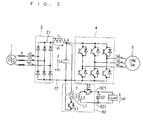
- FIGS. 1 and 2 each conceptually illustrate a power converter according to this preferred embodiment.
- the power converters each include a first power-supply line 21, a second power-supply line 22, a rectifier circuit 2, a capacitor Cd, a reactor Ld, an inverter 4, and a switching power-supply circuit 61 (or a switching power-supply circuit 62).
- FIGS. 1 and 2 show an ac power supply 1 that supplies power to the power converter, and a motor 5 that is supplied with the output from the inverter 4. Also, FIG. 1 shows a capacitor Cdc and a driven part Load that are supplied with the output of the switching power-supply circuit 61, and FIG. 2 shows a capacitor C2 and a driven part Load that are supplied with the output of the switching power-supply circuit 62.
- the capacitor Cdc or C2 smoothes the output of the switching power-supply circuit 61 or 62 and supplies it to the driven part Load.
- This preferred embodiment adopts a three-phase alternating-current power supply as the ac power supply 1.
- the motor 5 can be regarded as a main load
- the load composed of the motor 5 and the inverter 4 can be regarded as a first load (which is hereinafter denoted as "4+5")
- the load ( FIG. 1 ) composed of the capacitor Cdc and the driven part Load can be regarded as a second load (which is hereinafter denoted as "Cdc+Load")
- the load ( FIG. 2 ) composed of the capacitor C2 and the driven part Load can be regarded as a second load (which is hereinafter denoted as "C2+Load").
- the rectifier circuit 2 is a diode bridge, which rectifies input currents iu1, iv1, iw1 from the ac power supply 1 and outputs a dc voltage between the first power-supply line 21 and the second power-supply line 22.
- the capacitor Cd is connected between the first power-supply line 21 and the second power-supply line 22.
- the reactor Ld is provided on the first power-supply line 21 between the rectifier circuit 2 and the capacitor Cd.
- the capacitor Cd and the reactor Ld form a dc resonant circuit.
- the inverter 4 in this preferred embodiment is a three-phase inverter, which receives a voltage vdc across both ends of the capacitor Cd and outputs alternating currents iu2, iv2, iw2 to the motor 5.
- the motor 5 is driven by the supply of the output of the inverter 4.
- Each of the switching power-supply circuits 61 and 62 is connected between the first power-supply line 21 and the second power-supply line 22. They are each connected to both ends of the capacitor Cd in FIGS. 1 and 2 , but they may be connected to both ends of the serial resonant circuit formed of the capacitor Cd and the reactor Ld, for example.
- the switching power-supply circuit 61 adopts a step-down chopper.
- the step-down chopper includes switches S1, S2, a coil Ldc, and output ends 611 and 612.
- the switches S 1 and S2 are connected in series between the first power-supply line 21 and the second power-supply line 22.
- the output ends 611 and 612 are connected respectively to both ends of the switch S2.
- the coil Ldc is connected in series to the switch S2 between the output ends 611 and 612.
- the second load, Cdc+Load is connected between the output ends 611 and 612.
- the switching power-supply circuit 62 adopts a flyback converter.
- the flyback converter 62 includes switches S1, S2, a transformer T, and output ends 621 and 622.
- the primary coil L1 of the transformer T is connected between the first power-supply line 21 and the second power-supply 22, and its secondary coil L2 is connected between the output ends 621 and 622.
- the switch S1 is series-connected to the coil L1 between the first power-supply line 21 and the second power-supply line 22.
- the switch S2 is series-connected to the coil L2 between the output ends 621 and 622.
- the second load, C2+Load is connected between the output ends 621 and 622.
- the switches S1 and S2 adopt IGBT modules composed of IGBTs (Insulated Gate Bipolar Transistors) and diodes.
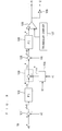
- FIG. 3 conceptually illustrates a controller 10 for controlling the power converter shown in FIG. 1 .
- the controller 10 includes subtracters 101, 105, command value corrector 103, control blocks 102, 104, 106, a triangular carrier generator 107, a comparator 108, and a NOT circuit 109.
- the subtracter 101 obtains a deviation ⁇ v0 of an output voltage v0 applied from the switching power-supply circuit 61 to the second load Cdc+Load, with respect to its command value v0*.
- the control block 102 performs PI control on the basis of the deviation ⁇ v0, so as to generate a command value idc* for a current idc flowing in the coil Ldc. According to this control, it is possible to make the voltage v0 close to the command value v0*, making it possible to stably apply the output voltage to the second load Cdc+Load.
- the command value corrector 103 corrects the command value idc* such that high-frequency components of the current iL flowing in the first power-supply line 21, with respect to the fundamental frequency of the input currents iu1, iv1, iwl, are consumed in the switching power-supply circuit 61.
- the command value corrector 103 corrects the command value idc* on the basis of a voltage vL applied to the reactor Ld. Specifically, the control block 104 multiplies the voltage vL and a gain K1 to obtain a correction value ⁇ idc*, and the command value corrector 103 subtracts the correction value ⁇ idc* from the command value idc* and outputs the result as a new command value idc*.
- the voltage vL adopted in this preferred embodiment is based on the potential of the reactor Ld on the rectifier circuit 2 side.
- control block 102 and the control block 106 described later, perform PI control, and therefore the output phase delays from the input phase in the control blocks 102 and 106. Accordingly, the phase of the correction command value ⁇ idc* may be shifted from the phase of the voltage vL in accordance with the phase delay.
- the phase of the correction command value ⁇ idc* may be delayed by 90° from the phase of the voltage vL even when no phase delay occurs in the control blocks 102 and 106. This is because, in the reactor Ld, the phase of the current iL delays by 90° from the phase of the voltage vL.
- the subtracter 105 obtains a deviation ⁇ idc between the corrected command value idc* and the current idc.
- the control block 106 performs PI control on the basis of the deviation ⁇ idc, so as to generate a command value v* for the voltage v applied to both ends of the switch S2. According to this control, it is possible to make the current idc close to the command value idc*, making it possible to precisely control the power consumption of the second load Cdc+Load.
- the triangular carrier generator 107 generates a triangular carrier synchronized to the inverter 4.
- the comparator 108 compares the command value v* and the triangular carrier, so as to generate a switching command r1 for the switch S 1.
- the switch S1 is controlled to on or off by the switching command r1.
- the switch S2 is controlled complementarily to the switch S1, and therefore a command r2 for the switch S2 is obtained by inputting the command r1 to the NOT circuit 109 and obtaining the output.
- the command values r1 and r2 are obtained by the controller 10, and so no high-speed microcomputer processing is required for the control of the switching power-supply circuit 61.
- the switching frequencies (50 to 100 kHz) of converters such as flyback converters and step-down choppers can be made larger than the switching frequency (6 kHz) of the inverter 4.
- the contents described above can be regarded as: performing the switching operation of the switching power-supply 61 with a duty based on the voltage vL applied to the reactor Ld, so as to supply power to the second load Cdc+Load from high-frequency components, with respect to the fundamental frequency of the input currents iu1, iv1 and iw1, of the current (-iL) flowing in the first power-supply line 21.
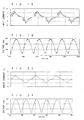
- FIG. 4 is a graph illustrating the time variation of the input current iu1 that is exhibited when the control of this preferred embodiment is performed.
- FIG. 5 is a graph illustrating the time variation of the voltage vdc across both ends of the capacitor Cd that is exhibited when the control of this preferred embodiment is performed.
- FIGS. 6 and 7 respectively show the waveforms of the input current iu1 and the voltage vdc that are exhibited before the control of this preferred embodiment is performed.
- the waveforms contain a lot of high-frequency components due to the serial resonance of the reactor Ld and the capacitor Cd.
- the graphs of FIGS. 4 to 7 show the results that were obtained when the command value v0* adopted 20 V, the driven part Load adopted resistance, the power consumption of the second load Cdc+Load adopted 20 W, and the power consumption of the motor 5 adopted 1.5 kW.
- FIGS. 4 and 6 show that performing this control suppresses high-frequency components contained in the input current iu1 (accordingly the input currents iv1, iw1, too) and the voltage vdc.
- the high-frequency components of power are smaller than the direct-current power supplied to the first load 4+5, so that the power consumption of the second load Cdc+Load that consumes them can be smaller than the power consumption in the first load 4+5.
- the current flowing in the switches S 1 and S2 of the switching power-supply circuit 61 can be smaller than the current flowing in the switching elements of the inverter 4. That is, the suppression provided by the control in the switching power-supply circuit 61 reduces switching loss, as compared with the switching for controlling harmonics by the control in the inverter 4.
- the switches S 1 and S2 can be of smaller current capacity, enabling size reduction of the switching power-supply circuit 61.
- the controller 10 is applicable also to the control of the power converter shown in FIG. 2 .
- the current i1 flowing in the coil L1 and its command value i1 * are adopted in place of the current idc and its command value idc*.
- a command value for the voltage across both ends of the coil L2 is adopted for the command value v*.
- FIG. 8 shows such a configuration as a controller 11.
- the controller 11 includes a subtracter 111, control blocks 112, 114, a correction command value 113, a triangular carrier generator 115, a comparator 116, and a NOT circuit 117.
- the subtracter 111 obtains a deviation ⁇ v0.
- the control block 112 performs PI control based on the deviation ⁇ v0 to generate a command value v*.
- the command corrector 113 corrects the command value v* such that high-frequency components of the current iL flowing in the first power-supply line 21, with respect to the fundamental frequency of the input currents iu1, iv1, iw1, are consumed in the switching power-supply circuit 61.
- the control block 114 multiplies the voltage vL and a gain K2 to obtain a correction value ⁇ v*, and the command value corrector 113 subtracts the correction value ⁇ v* from the command value v* and outputs the result as a new command value v*.
- phase of the correction command value ⁇ v* may be shifted from the phase of the voltage vL according to the phase delay.
- the triangular carrier generator 115 generates a triangular carrier synchronized to the inverter 4.
- the comparator 116 compares the corrected command value v* and the triangular carrier to generate a command value r1.
- a command value r2 is obtained by the NOT circuit 117 complementarily to the command value r1.
- high-frequency components contained in the current (-iL), with respect to the fundamental frequency of the input currents iu1, iv1, iwl, can be consumed in the second load Cdc+Load, C2+Load. It is thus possible to suppress the high-frequency components of the input currents iu1, iv1, iw1 to the rectifier circuit 2, and to suppress high-frequency disturbance to the ac power supply 1.
- the voltage v0 in this preferred embodiment can be adopted e.g. as a power-supply voltage of electrical equipment used in a motor driving system for an air conditioner, or a power-supply voltage for inverter control.
- FIG. 9 conceptually illustrates a power converter according to this preferred embodiment.
- a first power-supply line 21, a second power-supply line 22, a rectifier circuit 2, a capacitor Cd, a reactor Ld, and an inverter 4 are configured in the same way as those of the power converter of the first preferred embodiment, and further, a switching power-supply circuit 6 is connected between the first power-supply line 21 and the second power-supply line 22.
- FIG. 9 shows an ac power supply 1 and a motor 5 as in FIGS. 1 and 2 , and it further shows a motor 7 that is supplied with the output of the switching power-supply circuit 6. With the load formed of the inverter 4 and the motor 5 being regarded as a first load 4+5, the motor 7 can be regarded as a second load.
- the switching power-supply circuit 6 is a three-phase inverter and has switches S31 to S36.
- IGBT modules are adopted as the switches S31 to S36.
- a three-phase inverter is controlled by microcomputer processing.
- FIG. 10 conceptually illustrates a controller 20 for controlling the power converter shown in FIG. 9 .
- the controller 20 includes subtracters 201, 205, 207, a command value corrector 203, control blocks 202, 204, 206, 208, a transformation block 209, a triangular carrier generator 210, and a PWM (Pulse Width Modulation) control block 211.
- PWM Pulse Width Modulation
- the subtracter 201 obtains a deviation ⁇ of the rotating speed ⁇ of the motor 7 with respect to its command value ⁇ *.
- the control block 202 performs PI control on the basis of the deviation ⁇ , so as to generate a command value iq* for the q-axis current iq flowing in the motor. According to this control, it is possible to make the rotating speed ⁇ close to the command value ⁇ *, and thus to rotate the motor 7 stably.
- the command value corrector 203 corrects the command value iq* such that high-frequency components with respect to the fundamental frequency of the input currents iu1, iv1, iw1 are consumed in the switching power-supply circuit 6.
- the command value corrector 203 corrects the command value iq* on the basis of the voltage vL applied to the reactor Ld. Specifically, the control block 204 multiplies the voltage vL and a gain K to obtain a correction value ⁇ iq*, and the command value corrector 203 subtracts the correction value ⁇ iq* from the command value iq* and outputs the result as a new command value iq*.
- the phase of the correction command value ⁇ iq* may be shifted from the phase of the voltage vL according to phase delays in the control block 202 and the control block 206 that perform PI control.
- the phase of the correction command value ⁇ iq* may be delayed by 90° from the phase of the voltage vL even when no phase delay occurs in the control blocks 202 and 206.
- the subtracter 205 obtains a deviation ⁇ iq between the corrected command value iq* and the q-axis current iq.
- the control block 206 performs PI control on the basis of the deviation ⁇ iq to generate a command value vq* for the q-axis voltage vq applied to the motor 7. According to this control, it is possible to make the q-axis current iq close to the command value iq*.
- the subtracter 207 obtains a deviation ⁇ id of the d-axis current id flowing in the motor 7 with respect to its command value id*.
- the control block 208 performs PI control on the basis of the deviation ⁇ id, so as to generate a command value vd* for the d-axis voltage vd applied to the motor 7. According to this control, it is possible to make the d-axis current id close to the command value id*. As mentioned above, the current iq is also made close to its command value iq*, and the power consumption of the motor 7 can thus be precisely controlled.
- the transformation block 209 transforms the coordinates from the d-q axis coordinate system to three-phase coordinate system. Accordingly, the command values vq* and vd* inputted to the transformation block 209 are converted to command values vu*, vv*, vw* for the three-phase voltages vu, vv, vw, and outputted from the transformation block 209.
- the triangular carrier generator 210 generates a triangular carrier synchronized to the inverter 4.
- the PWM control block 211 generates commands r31 to r36 respectively for the switches S31 to S36, on the basis of the command values vu*, vv*, vw* and the triangular carrier.
- the switch S31 and the switch S34, the switch S32 and the switch S35, and the switch S33 and the switch S36, are controlled complementarily.
- the contents described above can be regarded as: performing the switching operation of the switching power-supply 6 with a duty based on the voltage vL applied to the reactor Ld, so as to supply power to the motor 7 from high-frequency components, with respect to the fundamental frequency of the input currents iu1, iv1, iwl, of the current (-iL) flowing in the first power-supply line 21.
- FIG. 11 is a graph illustrating the time variation of the input current iu1 that is exhibited when the control of this preferred embodiment is performed.
- FIG. 12 is a graph showing the time variation of the voltage vdc across both ends of the capacitor Cd that is exhibited when the control of this preferred embodiment is performed.
- FIGS. 13 and 14 respectively show the waveforms of the input current iu1 and the voltage vdc that are exhibited before the control of this preferred embodiment is performed.
- the waveforms contain a lot of high-frequency components due to the serial resonance of the reactor Ld and the capacitor Cd.
- the graphs of FIGS. 11 to 14 show the results that were obtained when the power consumption of the motor 5 adopted 1.5 kW, the command value ⁇ * for the motor 7 adopted 500 rpm, and the output power of the motor 7 adopted 20 W.
- FIGS. 11 and 13 show that performing this control suppresses the high-frequency components contained in the input current iu1 (accordingly the input currents iv1, iwl, too) and the voltage vdc.
- the power consumption of the motor 7 is set at 20 W, and also that the power consumption in the motor 5 is about 1.5 kW, it is known that the high-frequency disturbance can be suppressed even when the power consumption in the switching power-supply circuit 6 is small. Thus, the switching loss in the switching power-supply circuit 6 can be reduced. Then, the switches S31 to S36 can be of smaller current capacity. This makes it possible to downsize the switching power-supply circuit 6.
- the switching frequency of the inverter adopted to the switching power-supply circuit 6 is generally about the same as the switching frequency of the inverter 4 (6 kHz). However, when the above-described control is performed with the switching power-supply circuit 6, the switches S31 to S36 are switched at a switching frequency of around 50 kHz. Accordingly, from the viewpoint of microcomputer processing, the controlling with the power converter described in the first preferred embodiment is desirable.
- FIG. 15 illustrates a configuration in which a single-phase alternating-current power supply is adopted as the ac power supply 1 in the power converter shown in FIG. 1 .
- the rectifier circuit 2 rectifies an input current ic from the ac power supply 1 and outputs direct-current voltage between the first power-supply line 21 and the second power-supply line 22. In other respects, it is configured in the same way as the power converter shown in FIG. 1 .
- FIG. 16 is a graph illustrating the time variation of the input current ic that is exhibited when the control of this preferred embodiment is performed.
- FIG. 17 is a graph illustrating the time variation of the voltage vdc that is exhibited when the control of this preferred embodiment is performed.
- FIGS. 18 and 19 respectively show the waveforms of the input current ic and the voltage vdc that are exhibited before the control of this preferred embodiment is performed.
- the waveforms contain a lot of high-frequency components due to the serial resonance of the reactor Ld and the capacitor Cd.
- FIGS. 16 and 18 show that performing this control suppresses the high-frequency components contained in the input current ic and the voltage vdc.
- FIGS. 20 and 21 respectively show the waveforms of the input current ic and the voltage vdc that are exhibited when high-frequency waves are reduced with the inverter 4, without performing the control of this preferred embodiment.
- FIGS. 16 and 20 show that the inverter 4 can reduce high-frequency waves to about the same extent as the control of this preferred embodiment. However, the switching frequency in the inverter 4 is high and thereby the switching loss is increased.
- FIGS. 20 and 21 show the results obtained when the inverter was controlled at a switching frequency of 50 kHz as the switching frequency of the inverter 4.
- the correction value ⁇ idc*, ⁇ iq*, inputted to the command value corrector 103, 203 may be calculated on the basis of the current (-iL) flowing in the first power-supply line.
- the contents can be regarded as: causing the switching power-supply circuit 61, 62, 6 to perform switching operation with a duty based on the current (-iL) flowing in the first power-supply line 21, so as to supply power to the second load Cdc+Load, C2+Load, 7, from high-frequency components of the current (-iL) with respect to the fundamental frequency of the input currents iu1, iv1, iw1, ic.
- This control is applicable also to control of power converters with no reactor Ld, and offers the same effects as those of the first to third preferred embodiments. That is, even when no reactor Ld is provided, there is a problem that harmonics occur due to the serial resonance of the capacitor Cd and the impedance z occurring between the ac power supply 1 and the rectifier circuit 2 , and providing the control as described above suppresses the harmonics also in such cases.
- the command value v*, vq* may be obtained on the basis of the voltage vL or the current (-iL) and the current idc, iq, and the switching operation of the switching power-supply circuit 61, 62, 6 may be controlled according to the command value v*, vq*.
- the voltage converters described above can all be provided in air conditioners, for example.
- Such an air conditioner includes a motor for a refrigerant compressor and a fan for air-cooling, and the refrigerant-compressor motor is supplied with the output of the inverter 4, and the air-cooling fan is supplied with the output of the switching power-supply circuit 61, 62, 6. Then, air conditioning is achieved by operating the fan to remove the latent heat of the refrigerant compressed by the refrigerant compressor.
- the air-cooling fan requires less power consumption and rotary control accuracy. Accordingly, the control using the voltage converter is suitable for such air conditioners.
Landscapes
- Engineering & Computer Science (AREA)
- Power Engineering (AREA)
- Inverter Devices (AREA)
- Dc-Dc Converters (AREA)
- Rectifiers (AREA)
- Control Of Ac Motors In General (AREA)
Abstract
Description
- The present invention relates to a power converter and its control method, and particularly to a power converter of a type commonly called "capacitor-less" and its control method.
- An air conditioner includes a motor for a refrigerant compressor, and a power converter for supplying desired power to the motor. A common power converter includes a converter, an inverter, and a smoothing capacitor between them, and converts power supplied from an alternating-current power supply. Also, a reactor is provided to improve the input power factor. For example, the capacity of the reactor is about 2 mH, and the capacitance of the capacitor is about 2000 µF.
- The reactor and capacitor are especially large-sized and heavy-weighted among the parts of the power converter. Also, they constitute a cause of increased loss due to heat generation.
- Accordingly, a technique is proposed in which the capacitance of the capacitor is reduced to downsize the capacitor. This technique is commonly called "capacitor-less".
- Techniques related to the present invention are shown below. Particularly, Non-Patent
Document 3 discloses a technique that further omits the reactor. - Non-Patent Document 1: Myint Ko Tun and one other, "New Type Sinusoidal Input UPS Controlled by DC Chopper Type Active Filter", the Transactions III of Heisei 14 (2002) IEEJ Industry Applications Society Conference, The Institute of Electrical Engineers of Japan, August Heisei 14 (2002), pp. 1301-1306
Non-Patent Document 2: Yoichi Ito and one other, "Capacitor-less PWM Inverter", The transactions of Showa 63 (1988) IEEJ Industry Applications Society National Conference, The Institute of Electrical Engineers of Japan, August Showa 63 (1988), pp. 445-450
Non-Patent Document 3: Hitoshi Haga and one other, "Method of Improving Input Current Waveform of Single-Phase Field Capacitor-less IPM Motor Driving Inverter", The Transactions I of Heisei 14 (2002) IEEJ Industry Applications Society Conference, August Heisei 14 (2002), pp. 415-418 - However, reducing the capacity of the reactor and capacitance of the capacitor increases the resonant frequency determined by the reactor and smoothing capacitor, and then a lot of high-frequency components are contained in the power-supply current waveform, causing high-frequency disturbance to the ac power supply. This is not preferable from the viewpoint of JIS standards (JIS61000-3-2), for example.
- Such high-frequency disturbance can be suppressed e.g. by controlling the switching operation of the inverter. However, this requires increasing the inverter switching frequency, e.g. up to about ten times the resonant frequency. This is not very desirable because this causes increased switching loss in the inverter.
- The present invention has been made by considering the conditions above, and an object of the present invention is to suppress high-frequency disturbance to an ac power supply.
- According to a first aspect of the power converter of the present invention, a power converter comprises: a rectifier circuit (2) that rectifies an input current (iu1, iv1, iw1; ic) from an alternating-current power supply (1) and outputs a direct-current voltage between a first power-supply line (21) and a second power-supply line (22), so as to apply said direct-current voltage to a first load (4+5); a capacitor (Cd) connected between said first power-supply line and said second power-supply line; and a switching power-supply circuit (61; 62; 6) connected between said first power-supply line and said second power-supply line, said switching power-supply circuit performing a switching operation with a duty based on a first current (-iL) flowing in said first power-supply line, to supply power to a second load (Cdc+Load; C2+Load; 7) from a high-frequency component of said first current with respect to a fundamental frequency of said input current.
- According to a second aspect of the power converter of the present invention, in the power converter of the first aspect, said switching power-supply circuit (61; 62) comprises a switch (S1, S2) that performs said switching operation according to a command value (idc*; idc*) that is obtained on the basis of: a deviation (Δv0) of an output voltage (v0) applied to said second load (Cdc+Load; C2+Load) from said switching power-supply circuit with respect to its command value (v0*); and said first current (-iL).
- According to a third aspect of the power converter of the present invention, in the power converter of the first aspect, said second load is a motor (7), and said switching power-supply circuit (6) comprises a switch (S31-S36) that performs said switching operation according to a command value (iq*) that is obtained on the basis of: a deviation (Δω) of a rotating speed (ω) of said motor with respect to its command value (ω*); and said first current (-iL).
- According to a fourth aspect of the power converter of the present invention, in the power converter of the first aspect, said switching power-supply circuit (61; 62; 6) comprises a switch (S1, S2; S1, S2; S31-S36) that performs said switching operation according to a command value (v*; v*; vq*) that is obtained on the basis of: said first current (-iL) and a second current (idc; idc; iq) flowing in said second load (Cdc+Load; C2+Load; 7).
- According to a fifth aspect of the power converter of the present invention, a power converter comprises: a rectifier circuit (2) that rectifies an input current (iu1, iv1, iw1; ic) from an alternating-current power supply (1) and outputs a direct-current voltage between a first power-supply line (21) and a second power-supply line (22), so as to apply said direct-current voltage to a first load (4+5); a capacitor (Cd) connected between said first power-supply line and said second power-supply line; a reactor (Ld) constituting a serial resonant circuit together with said capacitor; and a switching power-supply circuit (61; 62; 6) connected between said first power-supply line and said second power-supply line, said switching power-supply circuit performing a switching operation with a duty based on a first voltage (vL) applied to said reactor, to supply power to a second load (Cdc+Load; C2+Load; 7) from a high-frequency component of a first current (-iL) flowing in said first power-supply line with respect to a fundamental frequency of said input current.
- According to a sixth aspect of the power converter of the present invention, in the power converter of the fifth aspect, said switching power-supply circuit (61; 62) comprises a switch (S1, S2) that performs said switching operation according to a command value (idc*; idc*) that is obtained on the basis of: a deviation (Δv0) of an output voltage (v0) applied to said second load (Cdc+Load; C2+Load) from said switching power-supply circuit with respect to its command value (v0*); and said first voltage (vL).
- According to a seventh aspect of the power converter of the present invention, in the power converter of the fifth aspect, said second load is a motor (7), and said switching power-supply circuit (6) comprises a switch (S31-S36) that performs said switching operation according to a command value (iq*) that is obtained on the basis of: a deviation (Δω) of a rotating speed (ω) of said motor with respect to its command value (ω*); and said first voltage (vL).
- According to an eighth aspect of the power converter of the present invention, in the power converter of the fifth aspect, said switching power-supply circuit (61; 62; 6) comprises a switch (S1, S2; S1, S2; S31-S36) that performs said switching operation according to a command value (v*; v*; vq*) that is obtained on the basis of: said first voltage (vL) and a second current (idc; idc; iq) flowing in said second load (Cdc+Load; C2+Load; 7).
- According to a ninth aspect of the power converter of the present invention, in the power converter of any of the second, third, sixth and seventh aspects, said switch (S1, S2; S1, S2; S31-S36) performs said switching operation according to a command value (v*; v*; vq*) that is obtained on the basis of: said command value (idc*; idc*; iq*) and a second current (idc; idc; iq) flowing in said second load (Cdc+Load; C2+Load; 7).
- According to a tenth aspect of the power converter of the present invention, in the power converter of any of the second to fourth, and sixth to ninth aspects, said first load (4+5) comprises a main load (5) and an inverter (4) that receives a voltage (vdc) across both ends of said capacitor and outputs an alternating current (iu2, iv2, iw2) to said main load, and said duty is determined by a comparison between said command value (idc; iq; v*; vq*) and a carrier for said inverter (4).
- According to an eleventh aspect of the power converter of the present invention, in the power converter of any of the first to ninth aspects, said first load (4+5) is comprised of a main load (5) and an inverter (4) that receives a voltage (vdc) across both ends of said capacitor and outputs an alternating current (iu2, iv2, iw2) to said main load.
- According to a first aspect of the air conditioner of the present invention, an air conditioner comprises: the power converter according to the eleventh aspect; a motor for a refrigerant compressor, said motor forming said main load (5); and an air-cooling fan that forms said second load (Cdc+Load; C2+Load; 7), and said air conditioner performs air conditioning by removing by said fan latent heat of a refrigerant compressed by said refrigerant compressor.
- According to a first aspect of the power converter controlling method of the present invention, a power converter comprises: a rectifier circuit (2) that rectifies an input current (iu1, iv1, iw1) from an alternating-current power supply (1) and outputs a direct-current voltage between a first power-supply line and a second power-supply line, so as to apply said direct-current voltage to a first load (4+5); a capacitor (Cd) connected between said first power-supply line and said second power-supply line; and a switching power-supply circuit (61; 62; 6) connected between said first power-supply line and said second power-supply line, and said power converter controlling method causes said switching power-supply circuit to perform a switching operation with a duty based on a first current (-iL) flowing in said first power-supply line, to supply power to a second load (Cdc+Load; C2+Load; 7) from a high-frequency component of said first current with respect to a fundamental frequency of said input current.
- According to a second aspect of the power converter controlling method of the present invention, in the power converter controlling method of the first aspect, said power converter controlling method causes said switching power-supply circuit (61; 62) to perform said switching operation according to a command value (idc*; idc*) that is obtained on the basis of: a deviation (Δv0) of an output voltage (v0) applied to said second load (Cdc+Load; C2+Load) from said switching power-supply circuit with respect to its command value (v0*); and said first current (-iL).
- According to a third aspect of the power converter controlling method of the present invention, in the power converter controlling method of the first aspect, said second load is a motor (7), and said power converter controlling method causes said switching power-supply circuit (6) to perform said switching operation according to a command value (iq*) that is obtained on the basis of: a deviation (Δω) of a rotating speed (ω) of said motor with respect to its command value (ω*); and said first current (-iL).
- According to a fourth aspect of the power converter controlling method of the present invention, in the power converter controlling method of the first aspect, said power converter controlling method causes said switching power-supply circuit (61; 62; 6) to perform said switching operation according to a command value (v*; v*; vq*) that is obtained on the basis of: said first current (-iL) and a second current (idc; idc; iq) flowing in said second load (Cdc+Load; C2+Load; 7).
- According to a fifth aspect of the power converter controlling method of the present invention, a power converter comprises: a rectifier circuit (2) that rectifies an input current (iu1, iv1, iw1) from an alternating-current power supply (1) and outputs a direct-current voltage between a first power-supply line and a second power-supply line, so as to apply said direct-current voltage to a first load (4+5); a capacitor (Cd) connected between said first power-supply line and said second power-supply line; a reactor (Ld) constituting a serial resonant circuit together with said capacitor; and a switching power-supply circuit (61; 62; 6) connected between said first power-supply line and said second power-supply line, and said power converter controlling method causes said switching power-supply circuit to perform a switching operation with a duty based on a first voltage (vL) applied to said reactor, to supply power to a second load (Cdc+Load; C2+Load; 7) from a high-frequency component of a first current (-iL) flowing in said first power-supply line with respect to a fundamental frequency of said input current.
- According to a sixth aspect of the power converter controlling method of the present invention, in the power converter controlling method of the fifth aspect, said power converter controlling method causes said switching power-supply circuit (61; 62) to perform said switching operation according to a command value (idc*; idc*) that is obtained on the basis of: a deviation (Δv0) of an output voltage (v0) applied to said second load (Cdc+Load; C2+Load) from said switching power-supply circuit with respect to its command value (v0*); and said first voltage (vL).
- According to a seventh aspect of the power converter controlling method of the present invention, in the power converter controlling method of the fifth aspect, said second load is a motor (7), and said power converter controlling method causes said switching power-supply circuit (6) to perform said switching operation according to a command value (iq*) that is obtained on the basis of: a deviation (Δω) of a rotating speed (ω) of said motor with respect to its command value (ω*); and said first voltage (vL).
- According to an eighth aspect of the power converter controlling method of the present invention, in the power converter controlling method of the fifth aspect, said power converter controlling method causes said switching power-supply circuit (61; 62; 6) to perform said switching operation according to a command value (v*; v*; vq*) that is obtained on the basis of: said first voltage (vL) and a second current (idc; idc; iq) flowing in said second load (Cdc+Load; C2+Load; 7).
- According to a ninth aspect of the power converter controlling method of the present invention, in the power converter controlling method of any of the second, third, sixth and seventh aspects, said power converter controlling method causes said switching power-supply circuit (61; 62; 6) to perform said switching operation according to a command value (v*; v*; vq*) that is obtained on the basis of: said command value (idc*; idc*; iq*) and a second current (idc; idc; iq) flowing in said second load (Cdc+Load; C2+Load; 7).
- According to a tenth aspect of the power converter controlling method of the present invention, in the power converter controlling method of any of the second to fourth, and sixth to ninth aspects, said first load (4+5) comprises a main load (5) and an inverter (4) that receives a voltage (vdc) across both ends of said capacitor and outputs an alternating current (iu2, iv2, iw2) to said main load, and said duty is determined by a comparison between said command value (idc; iq; v*; vq*) and a carrier for said inverter (4).
- According to any of the first, fourth, fifth and eighth aspects of the power converter of the present invention, or according to any of the first, fourth, fifth and eighth aspects of the power converter controlling method, the second load consumes a high-frequency component contained in the first current with respect to the fundamental frequency of the input current, which makes it possible to suppress the high-frequency component of the input current to the rectifier circuit and to suppress high-frequency disturbance to the alternating-current power supply.
- According to the second or sixth aspect of the power converter of the present invention, or according to the second or sixth aspect of the power converter controlling method, it is possible to stably apply the output voltage to the second load.
- According to the third or seventh aspect of the power converter of the present invention, or the third or seventh aspect of the power converter controlling method, it is possible to stably rotate the motor.
- According to the ninth aspect of the power converter of the present invention or the ninth aspect of the power converter controlling method, it is possible to precisely control the power consumption of the second load.
- According to the tenth aspect of the power converter of the present invention or the tenth aspect of the power converter controlling method, it is possible to synchronize the switching of the switching power-supply circuit with the switching of the inverter.
- According to the eleventh aspect of the power converter of the present invention, the switching loss in the inverter is small.
- According to the first aspect of the air conditioner of the present invention, it is suitable for the control using the power converter of the eleventh aspect because the air-cooling fan requires less power consumption and rotary control accuracy than the motor for a refrigerant compressor.
- These and other objects, features, aspects and advantages of the present invention will become more apparent from the following detailed description of the present invention when taken in conjunction with the accompanying drawings.
-
- [
FIG. 1 ] A diagram conceptually illustrating a power converter that is described in a first preferred embodiment. - [
FIG. 2 ] A diagram conceptually illustrating a power converter that is described in the first preferred embodiment. - [
FIG. 3 ] A diagram conceptually illustrating acontroller 10 for the power converter. - [
FIG. 4 ] A graph illustrating an input current iu1 that is exhibited when the control described in the first preferred embodiment is performed. - [
FIG. 5 ] A graph illustrating a voltage vdc that is exhibited when the control described in the first preferred embodiment is performed. - [
FIG. 6 ] A graph illustrating the input current iu1 that is exhibited before the control described in the first preferred embodiment is performed. - [
FIG. 7 ] A graph illustrating the voltage vdc that is exhibited before the control described in the first preferred embodiment is performed. - [
FIG. 8 ] A diagram conceptually illustrating acontroller 11 for the power converter. - [
FIG.9 ] A diagram conceptually illustrating a power converter that is described in a second preferred embodiment. - [
FIG. 10 ] A diagram conceptually illustrating acontroller 20 for the power converter. - [
FIG. 11 ] A graph illustrating the input current iu1 that is exhibited when the control described in the second preferred embodiment is performed. - [
FIG. 12 ] A graph illustrating the voltage vdc that is exhibited when the control described in the second preferred embodiment is performed. - [
FIG. 13 ] A graph illustrating the input current iu1 that is exhibited before the control described in the second preferred embodiment is performed. - [
FIG. 14 ] A graph illustrating the voltage vdc that is exhibited before the control described in the second preferred embodiment is performed. - [
FIG. 15 ] A diagram conceptually illustrating a power converter that is described in a third preferred embodiment. - [
FIG. 16 ] A graph illustrating an input current ic that is exhibited when the control described in the third preferred embodiment is performed. - [
FIG. 17 ] A graph illustrating a voltage vdc that is exhibited when the control described in the third preferred embodiment is performed. - [
FIG. 18 ] A graph illustrating the input current ic that is exhibited before the control described in the third preferred embodiment is performed. - [
FIG. 19 ] A graph illustrating the voltage vdc that is exhibited before the control described in the third preferred embodiment is performed. - [
FIG. 20 ] A graph illustrating the input current ic that is exhibited when the suppression of harmonics is performed withinverter 4. - [
FIG. 21 ] A graph illustrating the voltage vdc that is exhibited when the suppression of harmonics is performed withinverter 4. -
FIGS. 1 and2 each conceptually illustrate a power converter according to this preferred embodiment. The power converters each include a first power-supply line 21, a second power-supply line 22, arectifier circuit 2, a capacitor Cd, a reactor Ld, aninverter 4, and a switching power-supply circuit 61 (or a switching power-supply circuit 62). -
FIGS. 1 and2 show anac power supply 1 that supplies power to the power converter, and amotor 5 that is supplied with the output from theinverter 4. Also,FIG. 1 shows a capacitor Cdc and a driven part Load that are supplied with the output of the switching power-supply circuit 61, andFIG. 2 shows a capacitor C2 and a driven part Load that are supplied with the output of the switching power-supply circuit 62. The capacitor Cdc or C2 smoothes the output of the switching power-supply circuit ac power supply 1. - The
motor 5 can be regarded as a main load, the load composed of themotor 5 and theinverter 4 can be regarded as a first load (which is hereinafter denoted as "4+5"), the load (FIG. 1 ) composed of the capacitor Cdc and the driven part Load can be regarded as a second load (which is hereinafter denoted as "Cdc+Load"), and the load (FIG. 2 ) composed of the capacitor C2 and the driven part Load can be regarded as a second load (which is hereinafter denoted as "C2+Load"). - In this preferred embodiment, the
rectifier circuit 2 is a diode bridge, which rectifies input currents iu1, iv1, iw1 from theac power supply 1 and outputs a dc voltage between the first power-supply line 21 and the second power-supply line 22. - The capacitor Cd is connected between the first power-
supply line 21 and the second power-supply line 22. The reactor Ld is provided on the first power-supply line 21 between therectifier circuit 2 and the capacitor Cd. The capacitor Cd and the reactor Ld form a dc resonant circuit. - The
inverter 4 in this preferred embodiment is a three-phase inverter, which receives a voltage vdc across both ends of the capacitor Cd and outputs alternating currents iu2, iv2, iw2 to themotor 5. Themotor 5 is driven by the supply of the output of theinverter 4. - Each of the switching power-
supply circuits supply line 21 and the second power-supply line 22. They are each connected to both ends of the capacitor Cd inFIGS. 1 and2 , but they may be connected to both ends of the serial resonant circuit formed of the capacitor Cd and the reactor Ld, for example. - In
FIG. 1 , the switching power-supply circuit 61 adopts a step-down chopper. The step-down chopper includes switches S1, S2, a coil Ldc, and output ends 611 and 612. Theswitches S 1 and S2 are connected in series between the first power-supply line 21 and the second power-supply line 22. The output ends 611 and 612 are connected respectively to both ends of the switch S2. The coil Ldc is connected in series to the switch S2 between the output ends 611 and 612. The second load, Cdc+Load, is connected between the output ends 611 and 612. - In
FIG. 2 , the switching power-supply circuit 62 adopts a flyback converter. Theflyback converter 62 includes switches S1, S2, a transformer T, and output ends 621 and 622. The primary coil L1 of the transformer T is connected between the first power-supply line 21 and the second power-supply 22, and its secondary coil L2 is connected between the output ends 621 and 622. The switch S1 is series-connected to the coil L1 between the first power-supply line 21 and the second power-supply line 22. The switch S2 is series-connected to the coil L2 between the output ends 621 and 622. The second load, C2+Load, is connected between the output ends 621 and 622. - In this preferred embodiment, the switches S1 and S2 adopt IGBT modules composed of IGBTs (Insulated Gate Bipolar Transistors) and diodes.
-
FIG. 3 conceptually illustrates acontroller 10 for controlling the power converter shown inFIG. 1 . - The
controller 10 includessubtracters command value corrector 103, control blocks 102, 104, 106, atriangular carrier generator 107, acomparator 108, and aNOT circuit 109. - The
subtracter 101 obtains a deviation Δv0 of an output voltage v0 applied from the switching power-supply circuit 61 to the second load Cdc+Load, with respect to its command value v0*. - The
control block 102 performs PI control on the basis of the deviation Δv0, so as to generate a command value idc* for a current idc flowing in the coil Ldc. According to this control, it is possible to make the voltage v0 close to the command value v0*, making it possible to stably apply the output voltage to the second load Cdc+Load. - The
command value corrector 103 corrects the command value idc* such that high-frequency components of the current iL flowing in the first power-supply line 21, with respect to the fundamental frequency of the input currents iu1, iv1, iwl, are consumed in the switching power-supply circuit 61. - In this preferred embodiment, the
command value corrector 103 corrects the command value idc* on the basis of a voltage vL applied to the reactor Ld. Specifically, thecontrol block 104 multiplies the voltage vL and a gain K1 to obtain a correction value Δidc*, and thecommand value corrector 103 subtracts the correction value Δidc* from the command value idc* and outputs the result as a new command value idc*. The voltage vL adopted in this preferred embodiment is based on the potential of the reactor Ld on therectifier circuit 2 side. - Now, the
control block 102, and the control block 106 described later, perform PI control, and therefore the output phase delays from the input phase in the control blocks 102 and 106. Accordingly, the phase of the correction command value Δidc* may be shifted from the phase of the voltage vL in accordance with the phase delay. - The phase of the correction command value Δidc* may be delayed by 90° from the phase of the voltage vL even when no phase delay occurs in the control blocks 102 and 106. This is because, in the reactor Ld, the phase of the current iL delays by 90° from the phase of the voltage vL.
- The
subtracter 105 obtains a deviation Δidc between the corrected command value idc* and the current idc. - The
control block 106 performs PI control on the basis of the deviation Δidc, so as to generate a command value v* for the voltage v applied to both ends of the switch S2. According to this control, it is possible to make the current idc close to the command value idc*, making it possible to precisely control the power consumption of the second load Cdc+Load. - The
triangular carrier generator 107 generates a triangular carrier synchronized to theinverter 4. - The
comparator 108 compares the command value v* and the triangular carrier, so as to generate a switching command r1 for theswitch S 1. The switch S1 is controlled to on or off by the switching command r1. The switch S2 is controlled complementarily to the switch S1, and therefore a command r2 for the switch S2 is obtained by inputting the command r1 to theNOT circuit 109 and obtaining the output. - The command values r1 and r2 are obtained by the
controller 10, and so no high-speed microcomputer processing is required for the control of the switching power-supply circuit 61. In general, the switching frequencies (50 to 100 kHz) of converters such as flyback converters and step-down choppers can be made larger than the switching frequency (6 kHz) of theinverter 4. - The contents described above can be regarded as: performing the switching operation of the switching power-
supply 61 with a duty based on the voltage vL applied to the reactor Ld, so as to supply power to the second load Cdc+Load from high-frequency components, with respect to the fundamental frequency of the input currents iu1, iv1 and iw1, of the current (-iL) flowing in the first power-supply line 21. - According to the above-described
controller 10 and its control, high-frequency components that are contained in the current (-iL), with respect to the fundamental frequency of the input currents iu1, iv1, iw1, can be consumed in the second load Cdc+Load. This makes it possible to suppress the high-frequency components of the input currents iu1, iv1, iw1 to therectifier circuit 2, and thus to suppress high-frequency disturbance to theac power supply 1. -
FIG. 4 is a graph illustrating the time variation of the input current iu1 that is exhibited when the control of this preferred embodiment is performed.FIG. 5 is a graph illustrating the time variation of the voltage vdc across both ends of the capacitor Cd that is exhibited when the control of this preferred embodiment is performed. For comparison withFIGS. 4 and 5, FIGS. 6 and 7 respectively show the waveforms of the input current iu1 and the voltage vdc that are exhibited before the control of this preferred embodiment is performed. The waveforms contain a lot of high-frequency components due to the serial resonance of the reactor Ld and the capacitor Cd. The graphs ofFIGS. 4 to 7 show the results that were obtained when the command value v0* adopted 20 V, the driven part Load adopted resistance, the power consumption of the second load Cdc+Load adopted 20 W, and the power consumption of themotor 5 adopted 1.5 kW. - Comparison between
FIGS. 4 and 6 , and comparison betweenFIGS. 5 and 7 , show that performing this control suppresses high-frequency components contained in the input current iu1 (accordingly the input currents iv1, iw1, too) and the voltage vdc. - Furthermore, the high-frequency components of power are smaller than the direct-current power supplied to the
first load 4+5, so that the power consumption of the second load Cdc+Load that consumes them can be smaller than the power consumption in thefirst load 4+5. Thus, it is known that high-frequency disturbance can be suppressed even when the power consumption of the switching power-supply circuit 61 is small. Accordingly, the current flowing in theswitches S 1 and S2 of the switching power-supply circuit 61 can be smaller than the current flowing in the switching elements of theinverter 4. That is, the suppression provided by the control in the switching power-supply circuit 61 reduces switching loss, as compared with the switching for controlling harmonics by the control in theinverter 4. Then, theswitches S 1 and S2 can be of smaller current capacity, enabling size reduction of the switching power-supply circuit 61. - The
controller 10 is applicable also to the control of the power converter shown inFIG. 2 . However, the current i1 flowing in the coil L1 and its command value i1 * are adopted in place of the current idc and its command value idc*. Also, a command value for the voltage across both ends of the coil L2 is adopted for the command value v*. - When the control of the power consumption of the second load Cdc+Load, C2+Load, does not require very high accuracy, it is not essential to provide the
subtracter 105 and thecontrol block 106 in thecontroller 10.FIG. 8 shows such a configuration as acontroller 11. - The
controller 11 includes asubtracter 111, control blocks 112, 114, acorrection command value 113, atriangular carrier generator 115, acomparator 116, and aNOT circuit 117. - Like the
subtracter 101 shown inFIG. 3 , thesubtracter 111 obtains a deviation Δv0. - The
control block 112 performs PI control based on the deviation Δv0 to generate a command value v*. - The
command corrector 113 corrects the command value v* such that high-frequency components of the current iL flowing in the first power-supply line 21, with respect to the fundamental frequency of the input currents iu1, iv1, iw1, are consumed in the switching power-supply circuit 61. Specifically, thecontrol block 114 multiplies the voltage vL and a gain K2 to obtain a correction value Δv*, and thecommand value corrector 113 subtracts the correction value Δv* from the command value v* and outputs the result as a new command value v*. - When a phase delay occurs in the
control block 112, the phase of the correction command value Δv* may be shifted from the phase of the voltage vL according to the phase delay. - The
triangular carrier generator 115 generates a triangular carrier synchronized to theinverter 4. - The
comparator 116 compares the corrected command value v* and the triangular carrier to generate a command value r1. A command value r2 is obtained by theNOT circuit 117 complementarily to the command value r1. - Also with the
controller 11 and its control, high-frequency components contained in the current (-iL), with respect to the fundamental frequency of the input currents iu1, iv1, iwl, can be consumed in the second load Cdc+Load, C2+Load. It is thus possible to suppress the high-frequency components of the input currents iu1, iv1, iw1 to therectifier circuit 2, and to suppress high-frequency disturbance to theac power supply 1. - The voltage v0 in this preferred embodiment can be adopted e.g. as a power-supply voltage of electrical equipment used in a motor driving system for an air conditioner, or a power-supply voltage for inverter control.
-
FIG. 9 conceptually illustrates a power converter according to this preferred embodiment. In this power converter, a first power-supply line 21, a second power-supply line 22, arectifier circuit 2, a capacitor Cd, a reactor Ld, and aninverter 4 are configured in the same way as those of the power converter of the first preferred embodiment, and further, a switching power-supply circuit 6 is connected between the first power-supply line 21 and the second power-supply line 22.FIG. 9 shows anac power supply 1 and amotor 5 as inFIGS. 1 and2 , and it further shows a motor 7 that is supplied with the output of the switching power-supply circuit 6. With the load formed of theinverter 4 and themotor 5 being regarded as afirst load 4+5, the motor 7 can be regarded as a second load. - The switching power-
supply circuit 6 is a three-phase inverter and has switches S31 to S36. In this preferred embodiment, IGBT modules are adopted as the switches S31 to S36. In general, a three-phase inverter is controlled by microcomputer processing. -
FIG. 10 conceptually illustrates acontroller 20 for controlling the power converter shown inFIG. 9 . - The
controller 20 includessubtracters command value corrector 203, control blocks 202, 204, 206, 208, atransformation block 209, atriangular carrier generator 210, and a PWM (Pulse Width Modulation)control block 211. - The
subtracter 201 obtains a deviation Δω of the rotating speed ω of the motor 7 with respect to its command value ω*. - The
control block 202 performs PI control on the basis of the deviation Δω, so as to generate a command value iq* for the q-axis current iq flowing in the motor. According to this control, it is possible to make the rotating speed ω close to the command value ω*, and thus to rotate the motor 7 stably. - The
command value corrector 203 corrects the command value iq* such that high-frequency components with respect to the fundamental frequency of the input currents iu1, iv1, iw1 are consumed in the switching power-supply circuit 6. - In this preferred embodiment, the
command value corrector 203 corrects the command value iq* on the basis of the voltage vL applied to the reactor Ld. Specifically, thecontrol block 204 multiplies the voltage vL and a gain K to obtain a correction value Δiq*, and thecommand value corrector 203 subtracts the correction value Δiq* from the command value iq* and outputs the result as a new command value iq*. - Now, as described in the first preferred embodiment, the phase of the correction command value Δiq* may be shifted from the phase of the voltage vL according to phase delays in the
control block 202 and the control block 206 that perform PI control. The phase of the correction command value Δiq* may be delayed by 90° from the phase of the voltage vL even when no phase delay occurs in the control blocks 202 and 206. - The
subtracter 205 obtains a deviation Δiq between the corrected command value iq* and the q-axis current iq. - The
control block 206 performs PI control on the basis of the deviation Δiq to generate a command value vq* for the q-axis voltage vq applied to the motor 7. According to this control, it is possible to make the q-axis current iq close to the command value iq*. - The subtracter 207 obtains a deviation Δid of the d-axis current id flowing in the motor 7 with respect to its command value id*.
- The
control block 208 performs PI control on the basis of the deviation Δid, so as to generate a command value vd* for the d-axis voltage vd applied to the motor 7. According to this control, it is possible to make the d-axis current id close to the command value id*. As mentioned above, the current iq is also made close to its command value iq*, and the power consumption of the motor 7 can thus be precisely controlled. - The
transformation block 209 transforms the coordinates from the d-q axis coordinate system to three-phase coordinate system. Accordingly, the command values vq* and vd* inputted to thetransformation block 209 are converted to command values vu*, vv*, vw* for the three-phase voltages vu, vv, vw, and outputted from thetransformation block 209. - The
triangular carrier generator 210 generates a triangular carrier synchronized to theinverter 4. - The
PWM control block 211 generates commands r31 to r36 respectively for the switches S31 to S36, on the basis of the command values vu*, vv*, vw* and the triangular carrier. The switch S31 and the switch S34, the switch S32 and the switch S35, and the switch S33 and the switch S36, are controlled complementarily. - The contents described above can be regarded as: performing the switching operation of the switching power-
supply 6 with a duty based on the voltage vL applied to the reactor Ld, so as to supply power to the motor 7 from high-frequency components, with respect to the fundamental frequency of the input currents iu1, iv1, iwl, of the current (-iL) flowing in the first power-supply line 21. - According to the above-described
controller 20 and its control, high-frequency components that are contained in the current (-iL), with respect to the fundamental frequency of the input currents iu1, iv1, iwl, can be consumed in the motor 7. This makes it possible to suppress the high-frequency components of the input currents iu1, iv1, iw1 to therectifier circuit 2, and to suppress high-frequency disturbance to theac power supply 1. -
FIG. 11 is a graph illustrating the time variation of the input current iu1 that is exhibited when the control of this preferred embodiment is performed.FIG. 12 is a graph showing the time variation of the voltage vdc across both ends of the capacitor Cd that is exhibited when the control of this preferred embodiment is performed. For comparison withFIGS. 11 and 12, FIGS. 13 and 14 respectively show the waveforms of the input current iu1 and the voltage vdc that are exhibited before the control of this preferred embodiment is performed. The waveforms contain a lot of high-frequency components due to the serial resonance of the reactor Ld and the capacitor Cd. The graphs ofFIGS. 11 to 14 show the results that were obtained when the power consumption of themotor 5 adopted 1.5 kW, the command value ω* for the motor 7 adopted 500 rpm, and the output power of the motor 7 adopted 20 W. - Comparison between
FIGS. 11 and 13 , and comparison betweenFIGS. 12 and 14 , show that performing this control suppresses the high-frequency components contained in the input current iu1 (accordingly the input currents iv1, iwl, too) and the voltage vdc. - Furthermore, considering that the power consumption of the motor 7 is set at 20 W, and also that the power consumption in the
motor 5 is about 1.5 kW, it is known that the high-frequency disturbance can be suppressed even when the power consumption in the switching power-supply circuit 6 is small. Thus, the switching loss in the switching power-supply circuit 6 can be reduced. Then, the switches S31 to S36 can be of smaller current capacity. This makes it possible to downsize the switching power-supply circuit 6. - The switching frequency of the inverter adopted to the switching power-
supply circuit 6 is generally about the same as the switching frequency of the inverter 4 (6 kHz). However, when the above-described control is performed with the switching power-supply circuit 6, the switches S31 to S36 are switched at a switching frequency of around 50 kHz. Accordingly, from the viewpoint of microcomputer processing, the controlling with the power converter described in the first preferred embodiment is desirable. -
FIG. 15 illustrates a configuration in which a single-phase alternating-current power supply is adopted as theac power supply 1 in the power converter shown inFIG. 1 . In this case, therectifier circuit 2 rectifies an input current ic from theac power supply 1 and outputs direct-current voltage between the first power-supply line 21 and the second power-supply line 22. In other respects, it is configured in the same way as the power converter shown inFIG. 1 . - Also with this power converter, performing control in the same way as described in the first preferred embodiment offers the same effects.
-
FIG. 16 is a graph illustrating the time variation of the input current ic that is exhibited when the control of this preferred embodiment is performed.FIG. 17 is a graph illustrating the time variation of the voltage vdc that is exhibited when the control of this preferred embodiment is performed. For comparison withFIGS. 16 and 17 ,FIGS. 18 and 19 respectively show the waveforms of the input current ic and the voltage vdc that are exhibited before the control of this preferred embodiment is performed. The waveforms contain a lot of high-frequency components due to the serial resonance of the reactor Ld and the capacitor Cd. - Comparison between
FIGS. 16 and18 , and comparison betweenFIGS. 17 and19 , show that performing this control suppresses the high-frequency components contained in the input current ic and the voltage vdc. - Also,
FIGS. 20 and 21 respectively show the waveforms of the input current ic and the voltage vdc that are exhibited when high-frequency waves are reduced with theinverter 4, without performing the control of this preferred embodiment. - Comparison between
FIGS. 16 and20 , and comparison betweenFIGS. 17 and21 , show that theinverter 4 can reduce high-frequency waves to about the same extent as the control of this preferred embodiment. However, the switching frequency in theinverter 4 is high and thereby the switching loss is increased.FIGS. 20 and 21 show the results obtained when the inverter was controlled at a switching frequency of 50 kHz as the switching frequency of theinverter 4. - The same applies also when the power converters shown in
FIGS. 2 and9 adopt a single-phase ac power supply as theac power supply 1. - In any of the first to third preferred embodiments, the correction value Δidc*, Δiq*, inputted to the
command value corrector - The contents can be regarded as: causing the switching power-
supply circuit supply line 21, so as to supply power to the second load Cdc+Load, C2+Load, 7, from high-frequency components of the current (-iL) with respect to the fundamental frequency of the input currents iu1, iv1, iw1, ic. - This control is applicable also to control of power converters with no reactor Ld, and offers the same effects as those of the first to third preferred embodiments. That is, even when no reactor Ld is provided, there is a problem that harmonics occur due to the serial resonance of the capacitor Cd and the impedance z occurring between the
ac power supply 1 and therectifier circuit 2 , and providing the control as described above suppresses the harmonics also in such cases. - Also, in any of the above-described preferred embodiments, when the voltage v0 or the rotating speed ω does not require high controllability, it is not essential to provide the
subtracters controllers supply circuit - The voltage converters described above can all be provided in air conditioners, for example. Such an air conditioner includes a motor for a refrigerant compressor and a fan for air-cooling, and the refrigerant-compressor motor is supplied with the output of the
inverter 4, and the air-cooling fan is supplied with the output of the switching power-supply circuit - As compared with the refrigerant-compressor motor, the air-cooling fan requires less power consumption and rotary control accuracy. Accordingly, the control using the voltage converter is suitable for such air conditioners.
- While the invention has been described in detail, the foregoing description is in all aspects illustrative and not restrictive. It is understood that numerous other modifications and variations can be devised without departing from the scope of the invention.
Claims (22)
- A power converter comprising:a rectifier circuit (2) that rectifies an input current (iu1, iv1, iw1; ic) from an alternating-current power supply (1) and outputs a direct-current voltage between a first power-supply line (21) and a second power-supply line (22), so as to apply said direct-current voltage to a first load (4+5);a capacitor (Cd) connected between said first power-supply line and said second power-supply line; anda switching power-supply circuit (61; 62; 6) connected between said first power-supply line and said second power-supply line, said switching power-supply circuit performing a switching operation with a duty based on a first current (-iL) flowing in said first power-supply line, to supply power to a second load (Cdc+Load; C2+Load; 7) from a high-frequency component of said first current with respect to a fundamental frequency of said input current.
- The power converter according to claim 1, wherein said switching power-supply circuit (61; 62) comprises a switch (S1, S2) that performs said switching operation according to a command value (idc*; idc*) that is obtained on the basis of: a deviation (Δv0) of an output voltage (v0) applied to said second load (Cdc+Load; C2+Load) from said switching power-supply circuit with respect to its command value (v0*); and said first current (-iL).
- The power converter according to claim 1,
wherein said second load is a motor (7), and
said switching power-supply circuit (6) comprises a switch (S31-S36) that performs said switching operation according to a command value (iq*) that is obtained on the basis of: a deviation (Δω) of a rotating speed (ω) of said motor with respect to its command value (ω*); and said first current (-iL). - The power converter according to claim 1, wherein said switching power-supply circuit (61; 62; 6) comprises a switch (S1, S2; S1, S2; S31-S36) that performs said switching operation according to a command value (v*; v*; vq*) that is obtained on the basis of: said first current (-iL) and a second current (idc; idc; iq) flowing in said second load (Cdc+Load; C2+Load; 7).
- A power converter comprising:a rectifier circuit (2) that rectifies an input current (iu1, iv1, iw1; ic) from an alternating-current power supply (1) and outputs a direct-current voltage between a first power-supply line (21) and a second power-supply line (22), so as to apply said direct-current voltage to a first load (4+5);a capacitor (Cd) connected between said first power-supply line and said second power-supply line;a reactor (Ld) constituting a serial resonant circuit together with said capacitor; anda switching power-supply circuit (61; 62; 6) connected between said first power-supply line and said second power-supply line, said switching power-supply circuit performing a switching operation with a duty based on a first voltage (vL) applied to said reactor, to supply power to a second load (Cdc+Load; C2+Load; 7) from a high-frequency component of a first current (-iL) flowing in said first power-supply line with respect to a fundamental frequency of said input current.
- The power converter according to claim 5, wherein said switching power-supply circuit (61; 62) comprises a switch (S1, S2) that performs said switching operation according to a command value (idc*; idc*) that is obtained on the basis of: a deviation (Δv0) of an output voltage (v0) applied to said second load (Cdc+Load; C2+Load) from said switching power-supply circuit with respect to its command value (v0*); and said first voltage (vL).
- The power converter according to claim 5,
wherein said second load is a motor (7), and
said switching power-supply circuit (6) comprises a switch (S31-S36) that performs said switching operation according to a command value (iq*) that is obtained on the basis of: a deviation (Δω) of a rotating speed (ω) of said motor with respect to its command value (ω*); and said first voltage (vL). - The power converter according to claim 5, wherein said switching power-supply circuit (61; 62; 6) comprises a switch (S1, S2; S1, S2; S31-S36) that performs said switching operation according to a command value (v*; v*; vq*) that is obtained on the basis of: said first voltage (vL) and a second current (idc; idc; iq) flowing in said second load (Cdc+Load; C2+Load; 7).
- The power converter according to any of claims 2, 3, 6 and 7, wherein said switch (S1, S2; S1, S2; S31-S36) performs said switching operation according to a command value (v*; v*; vq*) that is obtained on the basis of: said command value (idc*; idc*; iq*) and a second current (idc; idc; iq) flowing in said second load (Cdc+Load; C2+Load; 7).
- The power converter according to any of claims 2 to 4, and 6 to 8,
wherein said first load (4+5) comprises a main load (5) and an inverter (4) that receives a voltage (vdc) across both ends of said capacitor and outputs an alternating current (iu2, iv2, iw2) to said main load, and
said duty is determined by a comparison between said command value (idc; iq; v*; vq*) and a carrier for said inverter (4). - The power converter according to any of claims 1 to 8,
wherein said first load (4+5) is comprised of a main load (5) and an inverter (4) that receives a voltage (vdc) across both ends of said capacitor and outputs an alternating current (iu2, iv2, iw2) to said main load. - An air conditioner comprising:the power converter according to claim 11;a motor for a refrigerant compressor, said motor forming said main load (5); andan air-cooling fan that forms said second load (Cdc+Load; C2+Load; 7),said air conditioner performing air conditioning by removing by said fan latent heat of a refrigerant compressed by said refrigerant compressor.
- A power converter controlling method for controlling a power converter, said power converter comprising:a rectifier circuit (2) that rectifies an input current (iu1, iv1, iw1) from an alternating-current power supply (1) and outputs a direct-current voltage between a first power-supply line and a second power-supply line, so as to apply said direct-current voltage to a first load (4+5);a capacitor (Cd) connected between said first power-supply line and said second power-supply line; anda switching power-supply circuit (61; 62; 6) connected between said first power-supply line and said second power-supply line,said power converter controlling method causing said switching power-supply circuit to perform a switching operation with a duty based on a first current (-iL) flowing in said first power-supply line, to supply power to a second load (Cdc+Load; C2+Load; 7) from a high-frequency component of said first current with respect to a fundamental frequency of said input current.
- The power converter controlling method according to claim 13, which causes said switching power-supply circuit (61; 62) to perform said switching operation according to a command value (idc*; idc*) that is obtained on the basis of: a deviation (Δv0) of an output voltage (v0) applied to said second load (Cdc+Load; C2+Load) from said switching power-supply circuit with respect to its command value (v0*); and said first current (-iL).
- The power converter controlling method according to claim 13,
wherein said second load is a motor (7), and
said power converter controlling method causes said switching power-supply circuit (6) to perform said switching operation according to a command value (iq*) that is obtained on the basis of: a deviation (Δω) of a rotating speed (ω) of said motor with respect to its command value (ω*); and said first current (-iL). - The power converter controlling method according to claim 13, which causes said switching power-supply circuit (61; 62; 6) to perform said switching operation according to a command value (v*; v*; vq*) that is obtained on the basis of: said first current (-iL) and a second current (idc; idc; iq) flowing in said second load (Cdc+Load; C2+Load; 7).
- A power converter controlling method for controlling a power converter, said power converter comprising:a rectifier circuit (2) that rectifies an input current (iu1, iv1, iw1) from an alternating-current power supply (1) and outputs a direct-current voltage between a first power-supply line and a second power-supply line, so as to apply said direct-current voltage to a first load (4+5);a capacitor (Cd) connected between said first power-supply line and said second power-supply line;a reactor (Ld) constituting a serial resonant circuit together with said capacitor; anda switching power-supply circuit (61; 62; 6) connected between said first power-supply line and said second power-supply line,said power converter controlling method causing said switching power-supply circuit to perform a switching operation with a duty based on a first voltage (vL) applied to said reactor, to supply power to a second load (Cdc+Load; C2+Load; 7) from a high-frequency component of a first current (-iL) flowing in said first power-supply line with respect to a fundamental frequency of said input current.
- The power converter controlling method according to claim 17, which causes said switching power-supply circuit (61; 62) to perform said switching operation according to a command value (idc*; idc*) that is obtained on the basis of: a deviation (Δv0) of an output voltage (v0) applied to said second load (Cdc+Load; C2+Load) from said switching power-supply circuit with respect to its command value (v0*); and said first voltage (vL).
- The power converter controlling method according to claim 17,
wherein said second load is a motor (7), and
said power converter controlling method causes said switching power-supply circuit (6) to perform said switching operation according to a command value (iq*) that is obtained on the basis of: a deviation (Δω) of a rotating speed (ω) of said motor with respect to its command value (ω*); and said first voltage (vL). - The power converter controlling method according to claim 17, which causes said switching power-supply circuit (61; 62; 6) to perform said switching operation according to a command value (v*; v*; vq*) that is obtained on the basis of: said first voltage (vL) and a second current (idc; idc; iq) flowing in said second load (Cdc+Load; C2+Load; 7).
- The power converter controlling method according to any of claims 14, 15, 18 and 19, which causes said switching power-supply circuit (61; 62; 6) to perform said switching operation according to a command value (v*; v*; vq*) that is obtained on the basis of: said command value (idc*; idc*; iq*) and a second current (idc; idc; iq) flowing in said second load (Cdc+Load; C2+Load; 7).
- The power converter controlling method according to any of claims 14 to 16, and 18 to 20,
wherein said first load (4+5) comprises a main load (5) and an inverter (4) that receives a voltage (vdc) across both ends of said capacitor and outputs an alternating current (iu2, iv2, iw2) to said main load, and
said duty is determined by a comparison between said command value (idc; iq; v*; vq*) and a carrier for said inverter (4).
Applications Claiming Priority (2)
| Application Number | Priority Date | Filing Date | Title |
|---|---|---|---|
| JP2006115814A JP4079178B2 (en) | 2006-04-19 | 2006-04-19 | Power converter, control method therefor, and air conditioner |
| PCT/JP2007/058085 WO2007123045A1 (en) | 2006-04-19 | 2007-04-12 | Power converter, its control method, and air conditioner |
Publications (3)
| Publication Number | Publication Date |
|---|---|
| EP2009774A1 true EP2009774A1 (en) | 2008-12-31 |
| EP2009774A4 EP2009774A4 (en) | 2017-04-26 |
| EP2009774B1 EP2009774B1 (en) | 2019-06-19 |
Family
ID=38624949
Family Applications (1)
| Application Number | Title | Priority Date | Filing Date |
|---|---|---|---|
| EP07741521.4A Active EP2009774B1 (en) | 2006-04-19 | 2007-04-12 | Power converter, its control method, and air conditioner |
Country Status (6)
| Country | Link |
|---|---|
| US (1) | US8269370B2 (en) |
| EP (1) | EP2009774B1 (en) |
| JP (1) | JP4079178B2 (en) |
| CN (1) | CN101385224B (en) |
| AU (1) | AU2007242096B2 (en) |
| WO (1) | WO2007123045A1 (en) |
Cited By (1)
| Publication number | Priority date | Publication date | Assignee | Title |
|---|---|---|---|---|
| EP3236575A4 (en) * | 2014-12-17 | 2018-06-13 | Daikin Industries, Ltd. | Charge/discharge circuit, control method for charge/discharge circuit, control device for charge/discharge circuit, and direct power converter |
Families Citing this family (24)
| Publication number | Priority date | Publication date | Assignee | Title |
|---|---|---|---|---|
| JP2011072142A (en) * | 2009-09-28 | 2011-04-07 | Daikin Industries Ltd | Power converter |
| CN102315782B (en) * | 2010-07-08 | 2013-10-16 | 晶宏半导体股份有限公司 | Power converter without electrolytic capacitor and power conversion method thereof |
| JP5212491B2 (en) * | 2011-01-18 | 2013-06-19 | ダイキン工業株式会社 | Power converter |
| EP2851631B1 (en) * | 2012-04-16 | 2020-03-11 | Mitsubishi Electric Corporation | Heat pump device, air conditioner, and cooling machine |
| JP5585643B2 (en) * | 2012-12-14 | 2014-09-10 | ダイキン工業株式会社 | Active filter control device |
| US20140268948A1 (en) * | 2013-03-15 | 2014-09-18 | Hamilton Sundstrand Corporation | Electromagnetic interference (emi) reduction in interleaved power converter |
| US9270168B2 (en) | 2013-03-15 | 2016-02-23 | Hamilton Sundstrand Corporation | Electromagnetic interference (EMI) reduction in multi-level power converter |
| JP5742980B1 (en) * | 2014-02-19 | 2015-07-01 | ダイキン工業株式会社 | Power converter control method |
| US9973129B2 (en) | 2015-06-12 | 2018-05-15 | Trane International Inc. | HVAC components having a variable speed drive with optimized power factor correction |
| US10284132B2 (en) | 2016-04-15 | 2019-05-07 | Emerson Climate Technologies, Inc. | Driver for high-frequency switching voltage converters |
| US10277115B2 (en) | 2016-04-15 | 2019-04-30 | Emerson Climate Technologies, Inc. | Filtering systems and methods for voltage control |
| US9933842B2 (en) | 2016-04-15 | 2018-04-03 | Emerson Climate Technologies, Inc. | Microcontroller architecture for power factor correction converter |
| US10305373B2 (en) | 2016-04-15 | 2019-05-28 | Emerson Climate Technologies, Inc. | Input reference signal generation systems and methods |
| US10312798B2 (en) | 2016-04-15 | 2019-06-04 | Emerson Electric Co. | Power factor correction circuits and methods including partial power factor correction operation for boost and buck power converters |
| US10656026B2 (en) | 2016-04-15 | 2020-05-19 | Emerson Climate Technologies, Inc. | Temperature sensing circuit for transmitting data across isolation barrier |
| US10763740B2 (en) | 2016-04-15 | 2020-09-01 | Emerson Climate Technologies, Inc. | Switch off time control systems and methods |
| CN107546890B (en) | 2016-06-28 | 2021-07-16 | 特灵国际有限公司 | Harmonic shunting motor, method, AC motor system and variable speed driving system |
| JP6826923B2 (en) * | 2017-03-22 | 2021-02-10 | 株式会社神戸製鋼所 | Compressor system |
| US10826357B2 (en) | 2017-06-28 | 2020-11-03 | Trane International Inc. | Harmonic shunting electric motor with faceted shaft for improved torque transmission |
| JP6638746B2 (en) * | 2018-01-31 | 2020-01-29 | ダイキン工業株式会社 | Inverter control method, AC load drive system, refrigeration circuit |
| JP6729650B2 (en) * | 2018-09-14 | 2020-07-22 | ダイキン工業株式会社 | Inverter control method, AC load power supply system, refrigeration circuit |
| CN109812932B (en) * | 2019-01-23 | 2020-11-13 | 奥克斯空调股份有限公司 | Temperature rise control method and device for power module of variable frequency air conditioner |
| CN113691173A (en) | 2021-07-23 | 2021-11-23 | 江苏东成工具科技有限公司 | Current control method |
| KR102741910B1 (en) * | 2022-12-27 | 2024-12-16 | 한국전자기술연구원 | Power imbalance prevention circuit and method of resonance type power converter |
Family Cites Families (15)
| Publication number | Priority date | Publication date | Assignee | Title |
|---|---|---|---|---|
| US4480298A (en) * | 1983-01-25 | 1984-10-30 | Westinghouse Electric Corp. | Multiple output DC-to-DC voltage converter apparatus |
| JP2812824B2 (en) * | 1990-11-14 | 1998-10-22 | 三菱電機株式会社 | DC-DC converter |
| US5341278A (en) * | 1992-08-20 | 1994-08-23 | Brooks Steven W | Switching pulsed resonant DC-DC converter power amplifier |
| FR2717014B1 (en) * | 1994-03-01 | 1996-04-26 | Telemecanique | PWM inverter control system. |
| JP3652811B2 (en) | 1996-08-30 | 2005-05-25 | 財団法人鉄道総合技術研究所 | Resonant current suppression device |
| JPH1198850A (en) | 1997-09-16 | 1999-04-09 | Mitsubishi Electric Corp | Air conditioner inverter device |
| JPH11187671A (en) | 1997-12-24 | 1999-07-09 | Toshiba Corp | Inverter device and refrigeration cycle device |
| US20010052704A1 (en) * | 1999-05-22 | 2001-12-20 | Capstone Turbine Corporation | Turbogenerator power control system |
| JP3616005B2 (en) * | 2000-12-20 | 2005-02-02 | 本田技研工業株式会社 | Hybrid vehicle cooling system |
| JP4210048B2 (en) * | 2001-08-09 | 2009-01-14 | 勲 高橋 | Inverter control method and inverter control circuit |
| EP2113999A3 (en) * | 2001-09-25 | 2010-01-06 | Daikin Industries, Ltd. | Phase current detection apparatus |
| US6813168B2 (en) * | 2002-11-18 | 2004-11-02 | Power Integrations, Inc. | Method and apparatus for providing input EMI filtering in power supplies |
| JP3772898B2 (en) * | 2004-09-08 | 2006-05-10 | ダイキン工業株式会社 | Multiphase current supply circuit and drive device |
| US20070091647A1 (en) * | 2004-11-12 | 2007-04-26 | Hiroshi Takemura | Switching power supply unit |
| US7541687B2 (en) * | 2006-03-10 | 2009-06-02 | Deere & Company | Method and system for managing an electrical output of a turbogenerator |
-
2006
- 2006-04-19 JP JP2006115814A patent/JP4079178B2/en not_active Expired - Fee Related
-
2007
- 2007-04-12 WO PCT/JP2007/058085 patent/WO2007123045A1/en not_active Ceased
- 2007-04-12 US US12/226,434 patent/US8269370B2/en active Active
- 2007-04-12 CN CN2007800054550A patent/CN101385224B/en active Active
- 2007-04-12 AU AU2007242096A patent/AU2007242096B2/en active Active
- 2007-04-12 EP EP07741521.4A patent/EP2009774B1/en active Active
Non-Patent Citations (1)
| Title |
|---|
| See references of WO2007123045A1 * |
Cited By (1)
| Publication number | Priority date | Publication date | Assignee | Title |
|---|---|---|---|---|
| EP3236575A4 (en) * | 2014-12-17 | 2018-06-13 | Daikin Industries, Ltd. | Charge/discharge circuit, control method for charge/discharge circuit, control device for charge/discharge circuit, and direct power converter |
Also Published As
| Publication number | Publication date |
|---|---|
| CN101385224A (en) | 2009-03-11 |
| JP4079178B2 (en) | 2008-04-23 |
| AU2007242096B2 (en) | 2010-09-16 |
| US20090102285A1 (en) | 2009-04-23 |
| CN101385224B (en) | 2011-06-29 |
| JP2007288971A (en) | 2007-11-01 |
| AU2007242096A1 (en) | 2007-11-01 |
| WO2007123045A1 (en) | 2007-11-01 |
| EP2009774A4 (en) | 2017-04-26 |
| US8269370B2 (en) | 2012-09-18 |
| EP2009774B1 (en) | 2019-06-19 |
Similar Documents
| Publication | Publication Date | Title |
|---|---|---|
| US8269370B2 (en) | Power converter and its control method and air conditioner | |
| EP3522355B1 (en) | Control device for direct power converter | |
| KR101594662B1 (en) | Power conversion device | |
| EP3220531B1 (en) | Power conversion device | |
| US9257931B2 (en) | Power conversion apparatus | |
| EP3176935B1 (en) | Electric power conversion device | |
| CN107567680B (en) | Variable speed drive with active converter | |
| EP3422551A1 (en) | Power conversion device, motor drive device, and refrigerator using same | |
| EP2273661A1 (en) | Converter control method | |
| CN113098304A (en) | Control circuit of three-phase Vienna rectifier and mixed carrier modulation method thereof | |
| US11437921B2 (en) | Direct power converter and control device to improve an input power factor | |
| CN108521849A (en) | The control device of power conversion device | |
| US20180183336A1 (en) | Apparatus for controlling dc link voltage in power cell of medium-voltage inverter | |
| US8749184B2 (en) | Control apparatus for electric motor | |
| JP4572595B2 (en) | CONVERTER CONTROL METHOD, CONVERTER CONTROL DEVICE, AIR CONDITIONER, ITS CONTROL METHOD AND CONTROL DEVICE | |
| EP3591828B1 (en) | Power supply control device, power conversion system, and power supply control method | |
| Tripathi et al. | High-performance off-line pulse width modulation without quarter wave symmetry for voltage-source inverter | |
| WO2023226011A1 (en) | Controlling of variable dc bus voltage in a motor | |
| Maswood et al. | Analysis of a PWM Voltage Source Inverter with PI Controller under Non-ideal conditions | |
| CN113541569B (en) | Motor drive device, method, air conditioner, and computer-readable storage medium | |
| Son et al. | Efficiency improvement in motor drive system with single phase diode rectifier and small DC-link capacitor | |
| JP2018191375A (en) | Active filter device and air conditioner using the same | |
| CN112886628A (en) | Shutoff angle compensation control method for improving stability of LCC-HVDC system under weak receiving end condition | |
| Abe et al. | Suppression method of increase in motor current at zero output voltage for an electrolytic capacitor-less inverter | |
| US12278576B2 (en) | Electric motor drive device |
Legal Events
| Date | Code | Title | Description |
|---|---|---|---|
| PUAI | Public reference made under article 153(3) epc to a published international application that has entered the european phase |
Free format text: ORIGINAL CODE: 0009012 |
|
| 17P | Request for examination filed |
Effective date: 20081016 |
|
| AK | Designated contracting states |
Kind code of ref document: A1 Designated state(s): AT BE BG CH CY CZ DE DK EE ES FI FR GB GR HU IE IS IT LI LT LU LV MC MT NL PL PT RO SE SI SK TR |
|
| AX | Request for extension of the european patent |
Extension state: AL BA HR MK RS |
|
| DAX | Request for extension of the european patent (deleted) | ||
| RA4 | Supplementary search report drawn up and despatched (corrected) |
Effective date: 20170324 |
|
| RIC1 | Information provided on ipc code assigned before grant |
Ipc: H02M 5/458 20060101ALI20170320BHEP Ipc: H02M 1/12 20060101ALI20170320BHEP Ipc: H02M 3/00 20060101AFI20170320BHEP Ipc: H02M 7/48 20070101ALI20170320BHEP |
|
| STAA | Information on the status of an ep patent application or granted ep patent |
Free format text: STATUS: EXAMINATION IS IN PROGRESS |
|
| 17Q | First examination report despatched |
Effective date: 20181108 |
|
| REG | Reference to a national code |
Ref country code: DE Ref legal event code: R079 Ref document number: 602007058629 Country of ref document: DE Free format text: PREVIOUS MAIN CLASS: H02M0003000000 Ipc: H02M0001120000 |
|
| GRAP | Despatch of communication of intention to grant a patent |
Free format text: ORIGINAL CODE: EPIDOSNIGR1 |
|
| STAA | Information on the status of an ep patent application or granted ep patent |
Free format text: STATUS: GRANT OF PATENT IS INTENDED |
|
| RIC1 | Information provided on ipc code assigned before grant |
Ipc: H02M 5/458 20060101ALI20190108BHEP Ipc: H02M 1/12 20060101AFI20190108BHEP |
|
| INTG | Intention to grant announced |
Effective date: 20190128 |
|
| GRAJ | Information related to disapproval of communication of intention to grant by the applicant or resumption of examination proceedings by the epo deleted |
Free format text: ORIGINAL CODE: EPIDOSDIGR1 |
|
| STAA | Information on the status of an ep patent application or granted ep patent |
Free format text: STATUS: EXAMINATION IS IN PROGRESS |
|
| GRAR | Information related to intention to grant a patent recorded |
Free format text: ORIGINAL CODE: EPIDOSNIGR71 |
|
| GRAS | Grant fee paid |
Free format text: ORIGINAL CODE: EPIDOSNIGR3 |
|
| STAA | Information on the status of an ep patent application or granted ep patent |
Free format text: STATUS: GRANT OF PATENT IS INTENDED |
|
| GRAA | (expected) grant |
Free format text: ORIGINAL CODE: 0009210 |
|
| STAA | Information on the status of an ep patent application or granted ep patent |
Free format text: STATUS: THE PATENT HAS BEEN GRANTED |
|
| INTC | Intention to grant announced (deleted) | ||
| INTG | Intention to grant announced |
Effective date: 20190508 |
|
| AK | Designated contracting states |
Kind code of ref document: B1 Designated state(s): AT BE BG CH CY CZ DE DK EE ES FI FR GB GR HU IE IS IT LI LT LU LV MC MT NL PL PT RO SE SI SK TR |
|
| REG | Reference to a national code |
Ref country code: GB Ref legal event code: FG4D |
|
| RIN1 | Information on inventor provided before grant (corrected) |
Inventor name: HAGA, HITOSHI |
|
| REG | Reference to a national code |
Ref country code: CH Ref legal event code: EP |
|
| REG | Reference to a national code |
Ref country code: IE Ref legal event code: FG4D |
|
| REG | Reference to a national code |
Ref country code: DE Ref legal event code: R096 Ref document number: 602007058629 Country of ref document: DE |
|
| REG | Reference to a national code |
Ref country code: AT Ref legal event code: REF Ref document number: 1146752 Country of ref document: AT Kind code of ref document: T Effective date: 20190715 |
|
| REG | Reference to a national code |
Ref country code: NL Ref legal event code: MP Effective date: 20190619 |
|
| PG25 | Lapsed in a contracting state [announced via postgrant information from national office to epo] |
Ref country code: LT Free format text: LAPSE BECAUSE OF FAILURE TO SUBMIT A TRANSLATION OF THE DESCRIPTION OR TO PAY THE FEE WITHIN THE PRESCRIBED TIME-LIMIT Effective date: 20190619 Ref country code: FI Free format text: LAPSE BECAUSE OF FAILURE TO SUBMIT A TRANSLATION OF THE DESCRIPTION OR TO PAY THE FEE WITHIN THE PRESCRIBED TIME-LIMIT Effective date: 20190619 Ref country code: SE Free format text: LAPSE BECAUSE OF FAILURE TO SUBMIT A TRANSLATION OF THE DESCRIPTION OR TO PAY THE FEE WITHIN THE PRESCRIBED TIME-LIMIT Effective date: 20190619 |
|
| REG | Reference to a national code |
Ref country code: LT Ref legal event code: MG4D |
|
| PG25 | Lapsed in a contracting state [announced via postgrant information from national office to epo] |
Ref country code: LV Free format text: LAPSE BECAUSE OF FAILURE TO SUBMIT A TRANSLATION OF THE DESCRIPTION OR TO PAY THE FEE WITHIN THE PRESCRIBED TIME-LIMIT Effective date: 20190619 Ref country code: GR Free format text: LAPSE BECAUSE OF FAILURE TO SUBMIT A TRANSLATION OF THE DESCRIPTION OR TO PAY THE FEE WITHIN THE PRESCRIBED TIME-LIMIT Effective date: 20190920 Ref country code: BG Free format text: LAPSE BECAUSE OF FAILURE TO SUBMIT A TRANSLATION OF THE DESCRIPTION OR TO PAY THE FEE WITHIN THE PRESCRIBED TIME-LIMIT Effective date: 20190919 |
|
| REG | Reference to a national code |
Ref country code: AT Ref legal event code: MK05 Ref document number: 1146752 Country of ref document: AT Kind code of ref document: T Effective date: 20190619 |
|
| PG25 | Lapsed in a contracting state [announced via postgrant information from national office to epo] |
Ref country code: AT Free format text: LAPSE BECAUSE OF FAILURE TO SUBMIT A TRANSLATION OF THE DESCRIPTION OR TO PAY THE FEE WITHIN THE PRESCRIBED TIME-LIMIT Effective date: 20190619 Ref country code: NL Free format text: LAPSE BECAUSE OF FAILURE TO SUBMIT A TRANSLATION OF THE DESCRIPTION OR TO PAY THE FEE WITHIN THE PRESCRIBED TIME-LIMIT Effective date: 20190619 Ref country code: RO Free format text: LAPSE BECAUSE OF FAILURE TO SUBMIT A TRANSLATION OF THE DESCRIPTION OR TO PAY THE FEE WITHIN THE PRESCRIBED TIME-LIMIT Effective date: 20190619 Ref country code: CZ Free format text: LAPSE BECAUSE OF FAILURE TO SUBMIT A TRANSLATION OF THE DESCRIPTION OR TO PAY THE FEE WITHIN THE PRESCRIBED TIME-LIMIT Effective date: 20190619 Ref country code: SK Free format text: LAPSE BECAUSE OF FAILURE TO SUBMIT A TRANSLATION OF THE DESCRIPTION OR TO PAY THE FEE WITHIN THE PRESCRIBED TIME-LIMIT Effective date: 20190619 Ref country code: PT Free format text: LAPSE BECAUSE OF FAILURE TO SUBMIT A TRANSLATION OF THE DESCRIPTION OR TO PAY THE FEE WITHIN THE PRESCRIBED TIME-LIMIT Effective date: 20191021 Ref country code: EE Free format text: LAPSE BECAUSE OF FAILURE TO SUBMIT A TRANSLATION OF THE DESCRIPTION OR TO PAY THE FEE WITHIN THE PRESCRIBED TIME-LIMIT Effective date: 20190619 |
|
| PG25 | Lapsed in a contracting state [announced via postgrant information from national office to epo] |
Ref country code: ES Free format text: LAPSE BECAUSE OF FAILURE TO SUBMIT A TRANSLATION OF THE DESCRIPTION OR TO PAY THE FEE WITHIN THE PRESCRIBED TIME-LIMIT Effective date: 20190619 Ref country code: IS Free format text: LAPSE BECAUSE OF FAILURE TO SUBMIT A TRANSLATION OF THE DESCRIPTION OR TO PAY THE FEE WITHIN THE PRESCRIBED TIME-LIMIT Effective date: 20191019 Ref country code: IT Free format text: LAPSE BECAUSE OF FAILURE TO SUBMIT A TRANSLATION OF THE DESCRIPTION OR TO PAY THE FEE WITHIN THE PRESCRIBED TIME-LIMIT Effective date: 20190619 |
|
| PG25 | Lapsed in a contracting state [announced via postgrant information from national office to epo] |
Ref country code: TR Free format text: LAPSE BECAUSE OF FAILURE TO SUBMIT A TRANSLATION OF THE DESCRIPTION OR TO PAY THE FEE WITHIN THE PRESCRIBED TIME-LIMIT Effective date: 20190619 |
|
| PG25 | Lapsed in a contracting state [announced via postgrant information from national office to epo] |
Ref country code: DK Free format text: LAPSE BECAUSE OF FAILURE TO SUBMIT A TRANSLATION OF THE DESCRIPTION OR TO PAY THE FEE WITHIN THE PRESCRIBED TIME-LIMIT Effective date: 20190619 Ref country code: PL Free format text: LAPSE BECAUSE OF FAILURE TO SUBMIT A TRANSLATION OF THE DESCRIPTION OR TO PAY THE FEE WITHIN THE PRESCRIBED TIME-LIMIT Effective date: 20190619 |
|
| PG25 | Lapsed in a contracting state [announced via postgrant information from national office to epo] |
Ref country code: IS Free format text: LAPSE BECAUSE OF FAILURE TO SUBMIT A TRANSLATION OF THE DESCRIPTION OR TO PAY THE FEE WITHIN THE PRESCRIBED TIME-LIMIT Effective date: 20200224 |
|
| REG | Reference to a national code |
Ref country code: DE Ref legal event code: R097 Ref document number: 602007058629 Country of ref document: DE |
|
| PLBE | No opposition filed within time limit |
Free format text: ORIGINAL CODE: 0009261 |
|
| STAA | Information on the status of an ep patent application or granted ep patent |
Free format text: STATUS: NO OPPOSITION FILED WITHIN TIME LIMIT |
|
| PG2D | Information on lapse in contracting state deleted |
Ref country code: IS |
|
| 26N | No opposition filed |
Effective date: 20200603 |
|
| PG25 | Lapsed in a contracting state [announced via postgrant information from national office to epo] |
Ref country code: SI Free format text: LAPSE BECAUSE OF FAILURE TO SUBMIT A TRANSLATION OF THE DESCRIPTION OR TO PAY THE FEE WITHIN THE PRESCRIBED TIME-LIMIT Effective date: 20190619 |
|
| PG25 | Lapsed in a contracting state [announced via postgrant information from national office to epo] |
Ref country code: MC Free format text: LAPSE BECAUSE OF FAILURE TO SUBMIT A TRANSLATION OF THE DESCRIPTION OR TO PAY THE FEE WITHIN THE PRESCRIBED TIME-LIMIT Effective date: 20190619 |
|
| REG | Reference to a national code |
Ref country code: CH Ref legal event code: PL |
|
| PG25 | Lapsed in a contracting state [announced via postgrant information from national office to epo] |
Ref country code: LU Free format text: LAPSE BECAUSE OF NON-PAYMENT OF DUE FEES Effective date: 20200412 Ref country code: LI Free format text: LAPSE BECAUSE OF NON-PAYMENT OF DUE FEES Effective date: 20200430 Ref country code: CH Free format text: LAPSE BECAUSE OF NON-PAYMENT OF DUE FEES Effective date: 20200430 |
|
| REG | Reference to a national code |
Ref country code: BE Ref legal event code: MM Effective date: 20200430 |
|
| PG25 | Lapsed in a contracting state [announced via postgrant information from national office to epo] |
Ref country code: BE Free format text: LAPSE BECAUSE OF NON-PAYMENT OF DUE FEES Effective date: 20200430 |
|
| PG25 | Lapsed in a contracting state [announced via postgrant information from national office to epo] |
Ref country code: IE Free format text: LAPSE BECAUSE OF NON-PAYMENT OF DUE FEES Effective date: 20200412 |
|
| PG25 | Lapsed in a contracting state [announced via postgrant information from national office to epo] |
Ref country code: MT Free format text: LAPSE BECAUSE OF FAILURE TO SUBMIT A TRANSLATION OF THE DESCRIPTION OR TO PAY THE FEE WITHIN THE PRESCRIBED TIME-LIMIT Effective date: 20190619 Ref country code: CY Free format text: LAPSE BECAUSE OF FAILURE TO SUBMIT A TRANSLATION OF THE DESCRIPTION OR TO PAY THE FEE WITHIN THE PRESCRIBED TIME-LIMIT Effective date: 20190619 |
|
| P01 | Opt-out of the competence of the unified patent court (upc) registered |
Effective date: 20230525 |
|
| PGFP | Annual fee paid to national office [announced via postgrant information from national office to epo] |
Ref country code: DE Payment date: 20250305 Year of fee payment: 19 |
|
| PGFP | Annual fee paid to national office [announced via postgrant information from national office to epo] |
Ref country code: GB Payment date: 20260313 Year of fee payment: 20 |
|
| PGFP | Annual fee paid to national office [announced via postgrant information from national office to epo] |
Ref country code: FR Payment date: 20260309 Year of fee payment: 20 |