EP2009752A1 - Electrooptic conversion module - Google Patents
Electrooptic conversion module Download PDFInfo
- Publication number
- EP2009752A1 EP2009752A1 EP07740961A EP07740961A EP2009752A1 EP 2009752 A1 EP2009752 A1 EP 2009752A1 EP 07740961 A EP07740961 A EP 07740961A EP 07740961 A EP07740961 A EP 07740961A EP 2009752 A1 EP2009752 A1 EP 2009752A1
- Authority
- EP
- European Patent Office
- Prior art keywords
- conversion module
- electric
- divided units
- optic conversion
- connector
- Prior art date
- Legal status (The legal status is an assumption and is not a legal conclusion. Google has not performed a legal analysis and makes no representation as to the accuracy of the status listed.)
- Withdrawn
Links
- 238000006243 chemical reaction Methods 0.000 title claims abstract description 64
- 230000003287 optical effect Effects 0.000 claims abstract description 91
- 230000004308 accommodation Effects 0.000 claims description 4
- 230000007257 malfunction Effects 0.000 abstract 1
- 230000000717 retained effect Effects 0.000 abstract 1
- 230000008054 signal transmission Effects 0.000 description 52
- 238000010586 diagram Methods 0.000 description 15
- 238000012986 modification Methods 0.000 description 13
- 230000004048 modification Effects 0.000 description 13
- 239000000758 substrate Substances 0.000 description 6
- 230000010354 integration Effects 0.000 description 3
- 238000000034 method Methods 0.000 description 3
- VYPSYNLAJGMNEJ-UHFFFAOYSA-N Silicium dioxide Chemical compound O=[Si]=O VYPSYNLAJGMNEJ-UHFFFAOYSA-N 0.000 description 2
- 230000005540 biological transmission Effects 0.000 description 2
- 238000005253 cladding Methods 0.000 description 2
- 239000002184 metal Substances 0.000 description 2
- 239000007769 metal material Substances 0.000 description 2
- 230000001902 propagating effect Effects 0.000 description 2
- 239000004065 semiconductor Substances 0.000 description 2
- 230000000694 effects Effects 0.000 description 1
- 239000000835 fiber Substances 0.000 description 1
- 239000000377 silicon dioxide Substances 0.000 description 1
- 229910000679 solder Inorganic materials 0.000 description 1
Images







Classifications
-
- G—PHYSICS
- G02—OPTICS
- G02B—OPTICAL ELEMENTS, SYSTEMS OR APPARATUS
- G02B6/00—Light guides; Structural details of arrangements comprising light guides and other optical elements, e.g. couplings
- G02B6/24—Coupling light guides
- G02B6/42—Coupling light guides with opto-electronic elements
- G02B6/4201—Packages, e.g. shape, construction, internal or external details
-
- G—PHYSICS
- G02—OPTICS
- G02B—OPTICAL ELEMENTS, SYSTEMS OR APPARATUS
- G02B6/00—Light guides; Structural details of arrangements comprising light guides and other optical elements, e.g. couplings
- G02B6/24—Coupling light guides
- G02B6/42—Coupling light guides with opto-electronic elements
- G02B6/4201—Packages, e.g. shape, construction, internal or external details
- G02B6/4219—Mechanical fixtures for holding or positioning the elements relative to each other in the couplings; Alignment methods for the elements, e.g. measuring or observing methods especially used therefor
- G02B6/4236—Fixing or mounting methods of the aligned elements
- G02B6/424—Mounting of the optical light guide
- G02B6/4243—Mounting of the optical light guide into a groove
-
- G—PHYSICS
- G02—OPTICS
- G02B—OPTICAL ELEMENTS, SYSTEMS OR APPARATUS
- G02B6/00—Light guides; Structural details of arrangements comprising light guides and other optical elements, e.g. couplings
- G02B6/24—Coupling light guides
- G02B6/42—Coupling light guides with opto-electronic elements
- G02B6/4201—Packages, e.g. shape, construction, internal or external details
- G02B6/4219—Mechanical fixtures for holding or positioning the elements relative to each other in the couplings; Alignment methods for the elements, e.g. measuring or observing methods especially used therefor
- G02B6/4236—Fixing or mounting methods of the aligned elements
- G02B6/4245—Mounting of the opto-electronic elements
-
- G—PHYSICS
- G02—OPTICS
- G02B—OPTICAL ELEMENTS, SYSTEMS OR APPARATUS
- G02B6/00—Light guides; Structural details of arrangements comprising light guides and other optical elements, e.g. couplings
- G02B6/24—Coupling light guides
- G02B6/42—Coupling light guides with opto-electronic elements
- G02B6/4201—Packages, e.g. shape, construction, internal or external details
- G02B6/4274—Electrical aspects
- G02B6/4278—Electrical aspects related to pluggable or demountable opto-electronic or electronic elements
-
- H—ELECTRICITY
- H01—ELECTRIC ELEMENTS
- H01S—DEVICES USING THE PROCESS OF LIGHT AMPLIFICATION BY STIMULATED EMISSION OF RADIATION [LASER] TO AMPLIFY OR GENERATE LIGHT; DEVICES USING STIMULATED EMISSION OF ELECTROMAGNETIC RADIATION IN WAVE RANGES OTHER THAN OPTICAL
- H01S5/00—Semiconductor lasers
- H01S5/02—Structural details or components not essential to laser action
- H01S5/022—Mountings; Housings
- H01S5/0225—Out-coupling of light
- H01S5/02251—Out-coupling of light using optical fibres
Definitions
- the present invention relates to an electric-optic conversion module.
- an electric-optic conversion module using a planar lightwave circuit has been known in optical communications such as FTTH (Fiber To The Home).
- a VCSEL Very-Cavity Surface-Emitting Laser
- LD laser diode
- PD photo diode
- various LSIs Large Scale Integration
- a Non-Patent Document 1 discloses a hybrid integration technique as a technique in the electric-optic conversion module.
- positions between an optical waveguide and semiconductor optical elements such as a laser diode and a photo diode are adjusted on a silica-based PLC substrate with high accuracy to achieve an optical connection.
- Non-Patent Document 1 Yuji Akahori, Ikuo Ogawa, Toshikazu Hashimoto, Takaharu Ohyama, Takuya Tanaka, Takeshi Kurosaki, and Yuichi Tohmori: NTT R&D, Vol.50, No.4, pp.294-302, 2001 .
- the VCSEL, the PD, the amplifier, and the driver are integrally mounted on the substrate in a combination of user specifications.
- the whole substrate should be replaced. This causes extra costs.
- the whole substrate, on which the normally operating amplifier and driver are mounted should be replaced.
- the driver with new one in order to drive the semiconductor optical elements at a higher speed the whole substrate, on which the normally operating VCSEL and PD are mounted, should be replaced. This is not economical.
- an object of the present invention to provide an electric-optic conversion module in which electronic components can be replaced at less cost.
- an electric-optic conversion module including: a functional section including an optoelectric conversion element and an auxiliary element of the optoelectric conversion element; and a connector which accommodates the functional section to electrically connect the functional section and an external device, wherein the functional section includes a plurality of divided units which are divided from one another according to functions or combination of the respective functions and which are removable from one another and removable from the connector.
- Each of the plurality of divided units is accommodated in the connector through a positioning section for defining an accommodation position of each of the divided units in the connector.
- the positioning section is formed by combination of a projection portion and a recessed portion, the projection portion being provided in an accommodation section of the connector and projecting toward a direction opposite to a fitting direction of the divided units, each of the divided units being provided with the recessed portion on a boundary surface with the adj acent divided unit, the projection portion being fitted into the recessed portion.
- the projection portion is a conductive pin having a columnar shape, and the recessed portion is provided with a conductive portion which is in electrically contact with the conductive pin.
- the projection portion is a conductive bump, and the recessed portion is provided with a conductive portion which is in electrically contact with the conductive pin.
- the positioning section is formed by combination of a projection portion and a recessed portion, the projection portion and the recessed portion being respectively provided on faces, which are opposed to one another, of the adjacent divided units accommodated in the connector, the projection portion and the recessed portion being fitted into one another.
- the projection portion and the recessed portion are respectively provided with different conductive portions which are in electrically contact with one another.
- the connector is provided with conductive connecting terminals which are extended outward and which are in electrically contact with the divided units, and the divided units are electrically connected to one another by electrically connecting the connecting terminals.
- An optical waveguide is optically connected to the optoelectric conversion element of the functional section.
- a plurality of divided units which are divided from one another according to functions or combination of the respective functions and which constitute a functional section having an optoelectric conversion element and an auxiliary element thereof, are removable from a connector which accommodates the divided units to electrically connect the divided units and an external device.
- Embodiments of the present invention will be described below with reference to Fig. 1 to 10 .
- the present invention is not limited to the embodiments.
- the Embodiments of the present invention show most preferred embodiments of the present invention.
- the wording of the invention and use of the invention are not limited to those of the embodiments.
- Fig. 1A illustrates a connection between electric-optic conversion modules 1 through an optical waveguide 2.
- Fig. 1B illustrates a state in which a plurality of divided units are fitted in a connector 100 of an electric-optic conversion module 1.
- Fig. 2 shows an optical signal transmission and reception unit 201, an amplifying unit 202, and a communication control unit 203 being fitted into a fitting section 120.
- Fig. 3 illustrates an external perspective view of the connector 100 with a cover member 111 lifted.
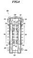
- Fig. 4 illustrates a top view of the connector 100 with the cover member 111 is lifted.
- Fig. 5A illustrates a top schematic diagram of a connection among a plurality of divided units.
- FIG. 5B illustrates a side schematic diagram of the connection among the plurality of divided units.
- Fig. 5C illustrates a bottom schematic diagram of the connection among the plurality of divided units.
- Fig. 6 illustrates a connection between the optical signal transmission and reception unit 201 and the amplifying unit 202.
- Fig. 7 shows a schematic sectional view of a state in which the optical signal transmission and reception unit 201 is fitted into the fitting section 120.
- the electric-optic conversionmodule 1 transmits an optical signal to another electric-optic conversion module 1 through the optical waveguide 2.
- the electric-optic conversion module 1 is electrically connected to an external device through electrode portions 101 exposed to the outside.
- two cores are covered with cladding when the optical transmission is performed bi-directionally or in parallel (a plurality of uni-directions), or one core is covered with cladding when the optical transmission is uni-directionally performed.
- the optical waveguide 2 has flexibility and is formed into a film shape.
- a plurality of divided units such as the optical signal transmission and reception unit 201, the amplifying unit 202, and the communication control unit 203 are fitted into a connector main body 110 of the connector 100, and the upper portion of the fitted plurality of divided units is to be covered with the cover member 111.
- the optical signal transmission and reception unit 201 includes a light receiving element such as a photo diode connected to the optical waveguide 2, and a light emitting element such as a laser diode connected to the optical waveguide 2.
- the optical signal transmission and reception unit 201 outputs an electric signal to the amplifying unit 202 based on an optical signal propagating through the optical waveguide 2, and outputs an optical signal to the optical waveguide 2 according to an electric signal inputted from the amplifying unit 202.
- the amplifying unit 202 includes an amplifying element such as a transistor which amplifies an electric signal.
- the amplifying unit 202 amplifies the electric signal supplied from the optical signal transmission and reception unit 201 or the electric signal to be outputted to the optical signal transmission and reception unit 201.
- the communication control unit 203 includes a control IC (Integrated Circuit) and the like.
- the communication control unit 203 controls the output of the electric signal into which the optical signal transmitted through the optical waveguide 2 is converted and the output of the optical signal to the optical waveguide 2 according to the electric signal supplied from the outside through the electrode portions 101.
- the plurality of divided units are divided from each other according to functions or combination of the respective functions.
- the optical signal transmission and reception unit 201, amplifying unit 202, and communication control unit 203 may freely be arranged.
- a single unit having functions of the amplifying unit 202 and communication control unit 203 may be provided.
- the plurality of divided units such as the optical signal transmission and reception unit 201, the amplifying unit 202, and the communication control unit 203 are brought into contact with a wall surface by pushing the divided units in a bottom direction of the fitting section 120 provided in the connector main body 110.
- the fitting section 120 includes socket contact portions 121 on both wall surfaces in a longitudinal direction (extended direction of the optical waveguide 2 when the optical signal transmission and reception unit 201 is connected) of the fitting section 120.
- the socket contact portions 121 are in contact with electrode terminals exposed outside the divided units when the divided units are fitted into the connector main body 110.
- An opening 122 for guiding the extending optical waveguide 2 to the outside is provided at the side of the optical signal transmission and reception unit 201 in a transverse direction of the fitting section 120.
- the transverse direction is orthogonal to the longitudinal direction.
- the fitting section 120 includes pins P1 to P4 projecting toward a direction opposite to a fitting direction of the divided units from a bottom face to which the plurality of divided units are connected when the divided units are in contact with socket contact portions 121 and fitted into the fitting section 120.
- the pins P1 to P4 are provided for defining the fitting positions of the plurality of divided units in the longitudinal direction.
- the pins P1 to P4 are made of metal having conductivity, and are substantially cylindrically-shaped.
- the pins P1 to P4 are electrically connected to recessed portions of the divided units described later.
- the shapes of the pins P1 to P4 are not limited to the substantially cylindrical shapes, but the pins P1 to P4 may be formed into plate shapes or polygonal shapes.
- the connector main body 110 is provided with the cover member 111 capable of turning around a shaft portion 112.
- the cover member 111 includes a pressing portion 113.
- the optical signal transmission and reception unit 201, the amplifying unit 202, and the communication control unit 203 are fitted into the fitting section 120, these units are pressed by the pressing member 113, which is rotated around the shaft portion 112 toward the fitting section 120, in a bottom direction of the fitting section 120 to fix these units in the fitting section 120.
- a pawl 114a and a pawl socket 114b are provided in the connector main body 110 and the cover member 111, respectively. The pawl 114a and the pawl socket 114b are used to fix the cover member 111 with the divided units pressed in the bottom direction of the fitting section 120.
- the divided units include boards inside thereof (not shown).
- the boards transmit and receive the optical signal, convert the optical signal into the electric signal, and perform the control thereof.
- upper portions of the optical signal transmission and reception unit 201, amplifying unit 202, and communication control unit 203, which are fitted in the fitting section 120, are covered with upper cases 211, 221, and 231, respectively, and lower portions of the divided units are covered with lower cases 212, 222, and 232, respectively.
- Connecting terminals 213, 223, and 233 are provided on side faces 205 of the lowercases 212, 222, and232, respectively.
- the connecting terminals 213, 223, and 233 electrically connected to the boards provided inside the divided units, and are in contact with the socket contact portions 121 when the divided units are fitted into the fitting section 120.
- Pin receiving holes 204 are formed in a connection part between the optical signal transmission and reception unit 201 and the amplifying unit 202, and in a connection part between the amplifying unit 202 and the communication control unit 203. The pins are inserted into the pin receiving holes 204 when the divided units are fitted into the fitting section 120.
- recessed portions 216 and 226 are formed on connecting surfaces 215 and 225 of the optical signal transmission and reception unit 201 and the amplifying unit 202, respectively.
- Each of the recessed portions 216 and 226 is substantially cylindrically-shaped with a radius of the pin.
- the pin receiving holes 204 are formed by the recessed portions 216 and 226.
- the recessed portions 216 and 226 constituting the pin receiving holes 204 are made of metal which is electrically connected to the boards provided inside the divided units, and the recessed portions 216 and 226 are elastically deformed to contact the pins P1 and P2. Therefore, the electrical connection between the optical signal transmission and reception unit 201 and the amplifying unit 202 is established by the recessed portions 216 and 226 through the pins P1 and P2. The same holds true for the connection between other divided units.
- Each of the socket contact portions 121 which are in contact with the optical signal transmission and reception unit 201, the amplifying unit 202, and the communication control unit 203 when these divided units are fitted into the fitting section 120, is made of conductive elastic metal material and is in the form of a long plate. As shown in Fig. 7 , each of the socket contact portions 121 is bent in the connector main body 110, extended in substantially parallel with the bottom of the connector 100 from the end of the bottom, and exposed to the outside as the electrode portion 101.
- the socket contact portions 121 are in contact with the connecting terminals 213 with the socket contact portions 121 elastically deformed as shown in Fig. 7 when the optical signal transmission and reception unit 201 is fitted into the fitting section 120. Therefore, the socket contact portions 121 are in contact with the connecting terminals 213 with the socket contact portions 121 biased toward the optical signal transmission and reception unit 201 from both side surfaces in the longitudinal direction of the fitting section 120. Thus, the optical signal transmission and reception unit 201 is fixed in the fitting section 120.
- the socket contact portions 121 are in contact with the connecting terminals 213 with certainty so that the electrical connection between the external device and the optical signal transmission and reception unit 201 can be established through the electrode portions 101.
- the plurality of divided units such as the optical signal transmission and reception unit 201, the amplifying unit 202, and the communication control unit 203 which convert the optical signal propagating through the optical waveguide 2 into the electric signal and convert the electric signal into the optical signal to output the optical signal to the optical waveguide 2, are fitted into the fitting section 120 of the connector main body 110 under the condition that electrode portions of the divided units are in contact with the socket contact portions 121 which are connected to the electrode portions 101 exposed to the outside.
- the electric-optic conversion module 1 includes the pins P1 to P4 for defining the connection positions of the divided units such as the optical signal transmission and reception unit 201, the amplifying unit 202, and the communication control unit 203 when the divided units are fitted into the fitting section 120, and the divided units have the recessed portions which receive the pins P1 to P4. With this structure, the plurality of divided units fitted into the fitting section 120 can accurately be positioned.
- the electric-optic conversion module 1 since the conductive pins P1 to P4 and the recessed portions as electrical terminals connected to the inside boards can be in contact with each other, the electrical connection between the adjacent divided units can be established.
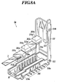
- FIG. 8A shows divided units being fitted into a fitting section of an electric-optic conversion module 1a according to the first modification.
- Fig. 8B illustrates a conductive bump H provided in the fitting section 120a.
- Fig. 8C illustrates a bottom of a connection part between an optical signal transmission and reception unit 201a and an amplifying unit 202a.
- the same reference numerals are given without adding explanations for those configurations that are the same as the above-described electric-optic conversion module 1.
- the electric-optic conversion module 1a is provided with a fitting section 120a in a connector main body 110a.
- An optical signal transmission and reception unit 201a, an amplifying unit 202a, and a communication control unit 203a are fitted into the fitting section 120a.
- the fitting section 120a includes conductive bumps H projecting toward a direction opposite to the fitting direction of the divided units from a bottom face to which the plurality of divided units are connected when the divided units are in contact with socket contact portions 121 and fitted into the fitting section 120a.
- a solder bump may be employed as the conductive bump H.
- Recessed portions (bottom connection portions) for connecting the conductive bumps H are provided on bottom faces (see an alternate long and short dash line of Fig. 8A ) of the optical signal transmission and reception unit 201a, the amplifying unit 202a, and the communication control unit 203a.
- the recessed portions are portions in which the divided units are in contact with each other and which are in contact with the conductive bump H when the divided units are fitted into the fitting section 120a.
- bottom connection portions 217 and 227 which are electrically connected to the boards provided inside, are provided on lower cases 212a and 222a of the optical signal transmission and reception unit 201a and the amplifying unit 202a, respectively.
- the bottom connection portions 217 and 227 are provided near positions at which the divided units are in contact with each other with the divided units fitted in the fitting section 120a, and are provided at bottom positions connected to the conductive bumps H.
- the optical signal transmission and reception unit 201a and the amplifying unit 202a are fitted into the fitting section 120a, the optical signal transmission and reception unit 201a and the amplifying unit 202a are electrically connected to each other through the bottom connection portions 217 and 227 and the conductive bumps H. The same holds true for the connection between other divided units.
- the electric-optic conversion module 1a is provided with the conductive bumps H on the bottom of the fitting section 120a, and the divided units such as the optical signal transmission and reception unit 201a, the amplifying unit 202a, and the communication control unit 203a are fixed by the conductive bumps H when these units are fitted into the fitting section 120a.
- the divided units can be fixed with certainty in the electric-optic conversion module 1a.
- connection portions of the divided units are connected to the conductive bumps H, and are electrically connected to the boards in the divided units, so that the divided units contacting each other can be electrically connected through the conductive bumps H.
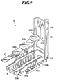
- FIG. 9 shows divided units being fitted into a fitting section of an electric-optic conversion module 1b according to the second modification.
- the same reference numerals are given without adding explanations for those configurations that are the same as the above-described electric-optic conversion module 1.
- the electric-optic conversion module 1b is provided with a fitting section 120b in a connector main body 110b.
- the divided units may be fixed in the fitting section 120b using the pins or the conductive bumps described above, or the divided units maybe fixed in the fitting section 120b only through the contact with the socket contact portions 121.
- each of electrode portions 101a is made of conductive elastic metal material and is in the form of a long plate.
- the electrode portions 101a are bent in a connector main body 110b to form the socket contact portions 121 of the fitting section 120b.
- the electrode portions 101a are exposed to the outside of the electric-optic conversion module 1.
- One electrode portion 101a is connected to another electrode portion 101a at the ends thereof through a conductive interelectrode connection section 101b.
- the terminals can electrically be connected to each other in the socket contact portions 121 through the interelectrode connection sections 101b of the electrode portions 101a exposed to the outside. That is, the optical signal transmission and reception unit 201b, the amplifying unit 202b, and the communication control unit 203b, which are fitted into the fitting section 120b, can electrically be connected to each other with ease through the interelectrode connection sections 101b with the divided units fitted into the connector main body 110b.
- FIG. 10A shows divided units being fitted into a fitting section of the electric-optic conversion module 1c according to a third modification.
- Fig. 10B illustrates a top view of an optical signal transmission and reception unit 201c, an amplifying unit 202c, and a communication control unit 203c.
- Fig. 10C illustrates a connection portion between the optical signal transmission and reception unit 201c and the communication control unit 202c.
- the same reference numerals are given without adding explanations for those configurations that are the same as the above-described electric-optic conversion module 1.
- the electric-optic conversion module 1c is provided with a fitting section 120c in a connector main body 110c.
- the optical signal transmission and reception unit 201c, the amplifying unit 202c, and the communication control unit 203c are fitted into the fitting section 120c.
- the divided units are fixed in the fitting section 120c only through the contact with the socket contact portion 121.
- the optical signal transmission and reception unit 201c, the amplifying unit 202c, and the communication control unit 203c include member connection portions 218, 228, and238, respectively which are electrically connected to the boards provided inside.
- the member connection portions 218, 228, and 238 are provided on faces on which the divided units are in contact with each other when the divided units are fitted into the fitting section 120c.
- the member connection portions 218, 228, and 238 are recessed portions and/or projection portions which are fitted into each other.
- the optical signal transmission and reception unit 201c is provided with the member connection portion 218 having the projected shape on the face on which the optical signal transmission and reception unit 201c is in contact with the amplifying unit 202c.
- the amplifying unit 202c is provided with the member connection portion 228 having the recessed shape on the face on which the amplifying unit 202c is in contact with the optical signal transmission and reception unit 201c.
- the member connection portions 218 and 228 are fitted into each other to connect the optical signal transmission and reception unit 201c and the amplifying unit 202c. The same holds true for the connection between other divided units.
- the divided units can be connected to each other with certainty, and the adjacent divided units can electrically be connected to each other.
- An electric-optic conversion module of the present invention is applicable in the optical communications field.
Landscapes
- Physics & Mathematics (AREA)
- General Physics & Mathematics (AREA)
- Optics & Photonics (AREA)
- Optical Couplings Of Light Guides (AREA)
- Connector Housings Or Holding Contact Members (AREA)
- Optical Integrated Circuits (AREA)
Abstract
Provided is an electrooptic conversion module, which can replace electronic parts more economically in case a malfunction occurs or in case an improvement is needed. In the electrooptic conversion module (1), a plurality of split units such as an optical signal transmit/receive unit (201) for converting an electric signal inputted into an optical signal to output the converted signal to the optical waveguide (2), an amplifying unit (202) and a communication control unit (203) are so fitted and retained in a fitting unit (120) to be connected with a cover member (111) exposed to the outside, that the terminal portions in the fitting portion (120) and the electrode portions of those split units contact with each other.
Description
- The present invention relates to an electric-optic conversion module.
- Conventionally, an electric-optic conversion module using a planar lightwave circuit (PLC) has been known in optical communications such as FTTH (Fiber To The Home). In the electric-optic conversion module, a VCSEL (Vertical-Cavity Surface-Emitting Laser), a laser diode (LD), a photo diode (PD), and various LSIs (Large Scale Integration) containing a driver for driving a photonic device such as a laser diode or containing an amplifier for amplifying a signal are disposed on a PLC substrate.
- For example, a Non-Patent
Document 1 discloses a hybrid integration technique as a technique in the electric-optic conversion module. In the hybrid integration technique, positions between an optical waveguide and semiconductor optical elements such as a laser diode and a photo diode are adjusted on a silica-based PLC substrate with high accuracy to achieve an optical connection.
Non-Patent Document 1: Yuji Akahori, Ikuo Ogawa, Toshikazu Hashimoto, Takaharu Ohyama, Takuya Tanaka, Takeshi Kurosaki, and Yuichi Tohmori: NTT R&D, Vol.50, No.4, pp.294-302, 2001. - In the conventional electric-optic conversion module, however, the VCSEL, the PD, the amplifier, and the driver are integrally mounted on the substrate in a combination of user specifications. When replacing one of the elements, the whole substrate should be replaced. This causes extra costs. For example, when replacing only a PD with new one, the whole substrate, on which the normally operating amplifier and driver are mounted, should be replaced. When replacing the driver with new one in order to drive the semiconductor optical elements at a higher speed, the whole substrate, on which the normally operating VCSEL and PD are mounted, should be replaced. This is not economical.
- In view of the foregoing, it is an object of the present invention to provide an electric-optic conversion module in which electronic components can be replaced at less cost.
- In order to solve the above-described problem, according to the present invention, there is provided an electric-optic conversion module including: a functional section including an optoelectric conversion element and an auxiliary element of the optoelectric conversion element; and a connector which accommodates the functional section to electrically connect the functional section and an external device, wherein the functional section includes a plurality of divided units which are divided from one another according to functions or combination of the respective functions and which are removable from one another and removable from the connector.
- Each of the plurality of divided units is accommodated in the connector through a positioning section for defining an accommodation position of each of the divided units in the connector.
- The positioning section is formed by combination of a projection portion and a recessed portion, the projection portion being provided in an accommodation section of the connector and projecting toward a direction opposite to a fitting direction of the divided units, each of the divided units being provided with the recessed portion on a boundary surface with the adj acent divided unit, the projection portion being fitted into the recessed portion.
- The projection portion is a conductive pin having a columnar shape, and the recessed portion is provided with a conductive portion which is in electrically contact with the conductive pin.
- The projection portion is a conductive bump, and the recessed portion is provided with a conductive portion which is in electrically contact with the conductive pin.
- The positioning section is formed by combination of a projection portion and a recessed portion, the projection portion and the recessed portion being respectively provided on faces, which are opposed to one another, of the adjacent divided units accommodated in the connector, the projection portion and the recessed portion being fitted into one another.
- The projection portion and the recessed portion are respectively provided with different conductive portions which are in electrically contact with one another.
- The connector is provided with conductive connecting terminals which are extended outward and which are in electrically contact with the divided units, and the divided units are electrically connected to one another by electrically connecting the connecting terminals.
- An optical waveguide is optically connected to the optoelectric conversion element of the functional section.
- According to the present invention, a plurality of divided units, which are divided from one another according to functions or combination of the respective functions and which constitute a functional section having an optoelectric conversion element and an auxiliary element thereof, are removable from a connector which accommodates the divided units to electrically connect the divided units and an external device. With this structure, in replacing a part of electronic components such as the optoelectric conversion elements or the auxiliary elements, it is only necessary to replace the divided unit including the element. Therefore, it is possible to replace the electronic component at less cost.
-
-
Fig. 1A is a schematic diagram illustrating a connection between electric-optic conversion modules through an optical waveguide. -
Fig. 1B is a schematic diagram illustrating a state in which a plurality of divided units are fitted in a connector of an electric-optic conversion module. -
Fig. 2 is a schematic diagram showing an optical signal transmission and reception unit, an amplifying unit, and a communication control unit being fitted into a fitting section. -
Fig. 3 is an external perspective view of the connector with a cover member lifted. -
Fig. 4 is a top view of the connector with the cover member is lifted. -
Fig. 5A is a top schematic diagram illustrating a connection among a plurality of divided units. -
Fig. 5B is a side schematic diagram illustrating the connection among the plurality of divided units. -
Fig. 5C is a bottom schematic diagram illustrating the connection among the plurality of divided units. -
Fig. 6 is a schematic diagram illustrating a connection between the optical signal transmission and reception unit and the amplifying unit. -
Fig. 7 is a schematic sectional view showing a state in which the optical signal transmission and reception unit is fitted into the fitting section. -
Fig. 8A is a schematic diagram showing divided units being fitted into a fitting section of an electric-optic conversion module according to a first modification. -
Fig. 8B is a schematic diagram illustrating a conductive bump provided in the fitting section. -
Fig. 8C is an enlarged bottom schematic diagram of a connection portion between an optical signal transmission and reception unit and an amplifying unit. -
Fig. 9 is a schematic diagram showing divided units being fitted into a fitting section of an electric-optic conversion module according to a second modification. -
Fig. 10A is a schematic diagram showing divided units being fitted into a fitting section of an electric-optic conversion module according to a third modification. -
Fig. 10B is a top view of an optical signal transmission and reception unit, an amplifying unit, and a communication control unit. -
Fig. 10C is an enlarged perspective view illustrating a connection portion between the optical signal transmission and reception unit and the communication control unit. - Embodiments of the present invention will be described below with reference to
Fig. 1 to 10 . The present invention is not limited to the embodiments. The Embodiments of the present invention show most preferred embodiments of the present invention. The wording of the invention and use of the invention are not limited to those of the embodiments. -
Fig. 1A illustrates a connection between electric-optic conversion modules 1 through anoptical waveguide 2.Fig. 1B illustrates a state in which a plurality of divided units are fitted in aconnector 100 of an electric-optic conversion module 1.Fig. 2 shows an optical signal transmission andreception unit 201, an amplifyingunit 202, and acommunication control unit 203 being fitted into afitting section 120.Fig. 3 illustrates an external perspective view of theconnector 100 with acover member 111 lifted.Fig. 4 illustrates a top view of theconnector 100 with thecover member 111 is lifted.Fig. 5A illustrates a top schematic diagram of a connection among a plurality of divided units.Fig. 5B illustrates a side schematic diagram of the connection among the plurality of divided units.Fig. 5C illustrates a bottom schematic diagram of the connection among the plurality of divided units.Fig. 6 illustrates a connection between the optical signal transmission andreception unit 201 and the amplifyingunit 202.Fig. 7 shows a schematic sectional view of a state in which the optical signal transmission andreception unit 201 is fitted into thefitting section 120. - As shown in
Fig. 1A , the electric-optic conversionmodule 1 transmits an optical signal to another electric-optic conversion module 1 through theoptical waveguide 2. The electric-optic conversion module 1 is electrically connected to an external device throughelectrode portions 101 exposed to the outside. In theoptical waveguide 2, two cores are covered with cladding when the optical transmission is performed bi-directionally or in parallel (a plurality of uni-directions), or one core is covered with cladding when the optical transmission is uni-directionally performed. Theoptical waveguide 2 has flexibility and is formed into a film shape. - As shown in
Fig. 1B , in the electric-optic conversion module 1, a plurality of divided units such as the optical signal transmission andreception unit 201, the amplifyingunit 202, and thecommunication control unit 203 are fitted into a connectormain body 110 of theconnector 100, and the upper portion of the fitted plurality of divided units is to be covered with thecover member 111. - The optical signal transmission and
reception unit 201 includes a light receiving element such as a photo diode connected to theoptical waveguide 2, and a light emitting element such as a laser diode connected to theoptical waveguide 2. The optical signal transmission andreception unit 201 outputs an electric signal to theamplifying unit 202 based on an optical signal propagating through theoptical waveguide 2, and outputs an optical signal to theoptical waveguide 2 according to an electric signal inputted from the amplifyingunit 202. The amplifyingunit 202 includes an amplifying element such as a transistor which amplifies an electric signal. The amplifyingunit 202 amplifies the electric signal supplied from the optical signal transmission andreception unit 201 or the electric signal to be outputted to the optical signal transmission andreception unit 201. Thecommunication control unit 203 includes a control IC (Integrated Circuit) and the like. In the optical signal transmission andreception unit 201 and amplifyingunit 202, thecommunication control unit 203 controls the output of the electric signal into which the optical signal transmitted through theoptical waveguide 2 is converted and the output of the optical signal to theoptical waveguide 2 according to the electric signal supplied from the outside through theelectrode portions 101. - The plurality of divided units (the optical signal transmission and
reception unit 201, amplifyingunit 202, and communication control unit 203) are divided from each other according to functions or combination of the respective functions. The optical signal transmission andreception unit 201, amplifyingunit 202, andcommunication control unit 203 may freely be arranged. For example, a single unit having functions of the amplifyingunit 202 andcommunication control unit 203 may be provided. - As shown in
Figs. 2 and3 , the plurality of divided units such as the optical signal transmission andreception unit 201, the amplifyingunit 202, and thecommunication control unit 203 are brought into contact with a wall surface by pushing the divided units in a bottom direction of thefitting section 120 provided in the connectormain body 110. Thus, the divided units are fitted into the connectormain body 110. Thefitting section 120 includessocket contact portions 121 on both wall surfaces in a longitudinal direction (extended direction of theoptical waveguide 2 when the optical signal transmission andreception unit 201 is connected) of thefitting section 120. Thesocket contact portions 121 are in contact with electrode terminals exposed outside the divided units when the divided units are fitted into the connectormain body 110. Anopening 122 for guiding the extendingoptical waveguide 2 to the outside is provided at the side of the optical signal transmission andreception unit 201 in a transverse direction of thefitting section 120. The transverse direction is orthogonal to the longitudinal direction. - As shown in
Figs. 2 to 4 , thefitting section 120 includes pins P1 to P4 projecting toward a direction opposite to a fitting direction of the divided units from a bottom face to which the plurality of divided units are connected when the divided units are in contact withsocket contact portions 121 and fitted into thefitting section 120. The pins P1 to P4 are provided for defining the fitting positions of the plurality of divided units in the longitudinal direction. The pins P1 to P4 are made of metal having conductivity, and are substantially cylindrically-shaped. The pins P1 to P4 are electrically connected to recessed portions of the divided units described later. The shapes of the pins P1 to P4 are not limited to the substantially cylindrical shapes, but the pins P1 to P4 may be formed into plate shapes or polygonal shapes. - As shown in
Figs. 2 to 4 , the connectormain body 110 is provided with thecover member 111 capable of turning around ashaft portion 112. Thecover member 111 includes apressing portion 113. When the optical signal transmission andreception unit 201, the amplifyingunit 202, and thecommunication control unit 203 are fitted into thefitting section 120, these units are pressed by the pressingmember 113, which is rotated around theshaft portion 112 toward thefitting section 120, in a bottom direction of thefitting section 120 to fix these units in thefitting section 120. Apawl 114a and apawl socket 114b are provided in the connectormain body 110 and thecover member 111, respectively. Thepawl 114a and thepawl socket 114b are used to fix thecover member 111 with the divided units pressed in the bottom direction of thefitting section 120. - The divided units include boards inside thereof (not shown). The boards transmit and receive the optical signal, convert the optical signal into the electric signal, and perform the control thereof. As shown in
Figs. 5A, 5B and 5C , upper portions of the optical signal transmission andreception unit 201, amplifyingunit 202, andcommunication control unit 203, which are fitted in thefitting section 120, are covered withupper cases lower cases - Connecting
terminals lowercases terminals socket contact portions 121 when the divided units are fitted into thefitting section 120. Pin receivingholes 204 are formed in a connection part between the optical signal transmission andreception unit 201 and the amplifyingunit 202, and in a connection part between the amplifyingunit 202 and thecommunication control unit 203. The pins are inserted into thepin receiving holes 204 when the divided units are fitted into thefitting section 120. - As shown in
Fig. 6 , for example, with respect to the connection part between the optical signal transmission andreception unit 201 and the amplifyingunit 202, recessedportions surfaces reception unit 201 and the amplifyingunit 202, respectively. Each of the recessedportions pin receiving holes 204 are formed by the recessedportions portions pin receiving holes 204 are made of metal which is electrically connected to the boards provided inside the divided units, and the recessedportions reception unit 201 and the amplifyingunit 202 is established by the recessedportions - Each of the
socket contact portions 121, which are in contact with the optical signal transmission andreception unit 201, the amplifyingunit 202, and thecommunication control unit 203 when these divided units are fitted into thefitting section 120, is made of conductive elastic metal material and is in the form of a long plate. As shown inFig. 7 , each of thesocket contact portions 121 is bent in the connectormain body 110, extended in substantially parallel with the bottom of theconnector 100 from the end of the bottom, and exposed to the outside as theelectrode portion 101. - For example, the
socket contact portions 121 are in contact with the connectingterminals 213 with thesocket contact portions 121 elastically deformed as shown inFig. 7 when the optical signal transmission andreception unit 201 is fitted into thefitting section 120. Therefore, thesocket contact portions 121 are in contact with the connectingterminals 213 with thesocket contact portions 121 biased toward the optical signal transmission andreception unit 201 from both side surfaces in the longitudinal direction of thefitting section 120. Thus, the optical signal transmission andreception unit 201 is fixed in thefitting section 120. Thesocket contact portions 121 are in contact with the connectingterminals 213 with certainty so that the electrical connection between the external device and the optical signal transmission andreception unit 201 can be established through theelectrode portions 101. - Thus, in the electric-
optic conversion module 1, the plurality of divided units such as the optical signal transmission andreception unit 201, the amplifyingunit 202, and thecommunication control unit 203 which convert the optical signal propagating through theoptical waveguide 2 into the electric signal and convert the electric signal into the optical signal to output the optical signal to theoptical waveguide 2, are fitted into thefitting section 120 of the connectormain body 110 under the condition that electrode portions of the divided units are in contact with thesocket contact portions 121 which are connected to theelectrode portions 101 exposed to the outside. - With this structure, in the electric-
optic conversion module 1, when replacement of one of the divided units is required because of replacement of a part of the electronic components, only the target divided unit can be replaced, so that the divided unit (electronic components) can be replaced at less cost. - The electric-
optic conversion module 1 includes the pins P1 to P4 for defining the connection positions of the divided units such as the optical signal transmission andreception unit 201, the amplifyingunit 202, and thecommunication control unit 203 when the divided units are fitted into thefitting section 120, and the divided units have the recessed portions which receive the pins P1 to P4. With this structure, the plurality of divided units fitted into thefitting section 120 can accurately be positioned. - Moreover, in the electric-
optic conversion module 1, since the conductive pins P1 to P4 and the recessed portions as electrical terminals connected to the inside boards can be in contact with each other, the electrical connection between the adjacent divided units can be established. - Next, an electric-optic conversion module 1a as a modification of the electric-
optic conversion module 1 will be described with reference toFigs. 8A ,8B and8C .Fig. 8A shows divided units being fitted into a fitting section of an electric-optic conversion module 1a according to the first modification.Fig. 8B illustrates a conductive bump H provided in thefitting section 120a.Fig. 8C illustrates a bottom of a connection part between an optical signal transmission andreception unit 201a and anamplifying unit 202a. InFigs. 8A to 8C , the same reference numerals are given without adding explanations for those configurations that are the same as the above-described electric-optic conversion module 1. - As shown in
Fig. 8A , the electric-optic conversion module 1a is provided with afitting section 120a in a connectormain body 110a. An optical signal transmission andreception unit 201a, anamplifying unit 202a, and acommunication control unit 203a are fitted into thefitting section 120a. As shown inFigs. 8A and8B , thefitting section 120a includes conductive bumps H projecting toward a direction opposite to the fitting direction of the divided units from a bottom face to which the plurality of divided units are connected when the divided units are in contact withsocket contact portions 121 and fitted into thefitting section 120a. For example, a solder bump may be employed as the conductive bump H. - Recessed portions (bottom connection portions) for connecting the conductive bumps H are provided on bottom faces (see an alternate long and short dash line of
Fig. 8A ) of the optical signal transmission andreception unit 201a, the amplifyingunit 202a, and thecommunication control unit 203a. The recessed portions are portions in which the divided units are in contact with each other and which are in contact with the conductive bump H when the divided units are fitted into thefitting section 120a. - Specifically, as shown in
Fig. 8C ,bottom connection portions lower cases reception unit 201a and theamplifying unit 202a, respectively. Thebottom connection portions fitting section 120a, and are provided at bottom positions connected to the conductive bumps H. When the optical signal transmission andreception unit 201a and theamplifying unit 202a are fitted into thefitting section 120a, the optical signal transmission andreception unit 201a and theamplifying unit 202a are electrically connected to each other through thebottom connection portions - As described above, the electric-optic conversion module 1a is provided with the conductive bumps H on the bottom of the
fitting section 120a, and the divided units such as the optical signal transmission andreception unit 201a, the amplifyingunit 202a, and thecommunication control unit 203a are fixed by the conductive bumps H when these units are fitted into thefitting section 120a. With this structure, the divided units can be fixed with certainty in the electric-optic conversion module 1a. - The connection portions of the divided units are connected to the conductive bumps H, and are electrically connected to the boards in the divided units, so that the divided units contacting each other can be electrically connected through the conductive bumps H.
- Next, an electric-optic conversion module 1b as a modification of the electric-
optic conversion module 1 will be described with reference toFig. 9. Fig. 9 shows divided units being fitted into a fitting section of an electric-optic conversion module 1b according to the second modification. InFig. 9 , the same reference numerals are given without adding explanations for those configurations that are the same as the above-described electric-optic conversion module 1. - As shown in
Fig. 9 , the electric-optic conversion module 1b is provided with afitting section 120b in a connectormain body 110b. An optical signal transmission and reception unit 201b, an amplifyingunit 202b, and a communication control unit 203bare fitted into thefitting section 120b. The divided units may be fixed in thefitting section 120b using the pins or the conductive bumps described above, or the divided units maybe fixed in thefitting section 120b only through the contact with thesocket contact portions 121. - As with the
electrode portions 101 described above, each ofelectrode portions 101a is made of conductive elastic metal material and is in the form of a long plate. Theelectrode portions 101a are bent in a connectormain body 110b to form thesocket contact portions 121 of thefitting section 120b. Theelectrode portions 101a are exposed to the outside of the electric-optic conversion module 1. Oneelectrode portion 101a is connected to anotherelectrode portion 101a at the ends thereof through a conductiveinterelectrode connection section 101b. - With this structure, in the electric-optic conversion module 1b, the terminals can electrically be connected to each other in the
socket contact portions 121 through theinterelectrode connection sections 101b of theelectrode portions 101a exposed to the outside. That is, the optical signal transmission and reception unit 201b, the amplifyingunit 202b, and thecommunication control unit 203b, which are fitted into thefitting section 120b, can electrically be connected to each other with ease through theinterelectrode connection sections 101b with the divided units fitted into the connectormain body 110b. - Next, an electric-optic conversion module 1c as a modification of the electric-
optic conversion module 1 will be described with reference toFigs. 10A ,10B and10C .Fig. 10A shows divided units being fitted into a fitting section of the electric-optic conversion module 1c according to a third modification.Fig. 10B illustrates a top view of an optical signal transmission andreception unit 201c, an amplifyingunit 202c, and acommunication control unit 203c.Fig. 10C illustrates a connection portion between the optical signal transmission andreception unit 201c and thecommunication control unit 202c. InFigs. 10A to 10C , the same reference numerals are given without adding explanations for those configurations that are the same as the above-described electric-optic conversion module 1. - As shown in
Fig. 10A , the electric-optic conversion module 1c is provided with afitting section 120c in a connectormain body 110c. The optical signal transmission andreception unit 201c, the amplifyingunit 202c, and thecommunication control unit 203c are fitted into thefitting section 120c. The divided units are fixed in thefitting section 120c only through the contact with thesocket contact portion 121. - As shown in
Fig. 10B , the optical signal transmission andreception unit 201c, the amplifyingunit 202c, and thecommunication control unit 203c includemember connection portions member connection portions fitting section 120c. Themember connection portions - Specifically, as shown in
Fig. 10C , the optical signal transmission andreception unit 201c is provided with themember connection portion 218 having the projected shape on the face on which the optical signal transmission andreception unit 201c is in contact with the amplifyingunit 202c. The amplifyingunit 202c is provided with themember connection portion 228 having the recessed shape on the face on which theamplifying unit 202c is in contact with the optical signal transmission andreception unit 201c. In fitting into thefitting section 120c, themember connection portions reception unit 201c and the amplifyingunit 202c. The same holds true for the connection between other divided units. - With this structure, in the electric-optic conversion module 1c, when the optical signal transmission and
reception unit 201c, the amplifyingunit 202c, and thecommunication control unit 203c are fitted into thefitting section 120c, the divided units can be connected to each other with certainty, and the adjacent divided units can electrically be connected to each other. - The description of the embodiments is exemplary, and the present invention is not limited to the embodiments. Various modifications and changes can appropriately be made in the detailed configurations of the electric-
optic conversion modules 1, 1a, 1b, and 1c of the embodiments. - An electric-optic conversion module of the present invention is applicable in the optical communications field.
-
- 1, 1a, 1b and 1c electric-optic conversion module
- 2 optical waveguide
- 100 connector
- 101 electrode portion
- 101a electrode portion
- 101b interelectrode connection section
- 110, 110a, 110b and 110c connector main body
- 111 cover member
- 112 shaft portion
- 113 pressing portion
- 114a pawl
- 114b pawl socket
- 120, 120a, 120b and 120c fitting section
- 121 socket contact portion
- 122 opening
- 201, 201a, 201b and 201c optical signal transmission and reception unit
- 202, 202a, 202b and 202c amplifying unit
- 203, 203a, 203b and 203c communication control unit
- 204 pin receiving hole
- 205 side face
- 211, 211a, 211b and 211c upper case
- 212, 212a, 212b and 212c lower case
- 213 connecting terminal
- 215 connection surface
- 216 recessed portion
- 217 bottom connection portion
- 218 member connection portion
- 221, 221a, 221b and 221c upper case
- 222, 222a, 222b and 222c lower case
- 223 connecting terminal
- 225 connection surface
- 226 recessed portion
- 227 bottom connection portion
- 228 member connection portion
- 231, 231a, 231b and 231c upper case
- 232, 232a, 232b and 232c lower case
- 233 connecting terminal
- 238 member connection portion
- P1 to P4 pin
- H conductive bump
Claims (9)
- An electric-optic conversion module comprising:a functional section including an optoelectric conversion element and an auxiliary element of the optoelectric conversion element; anda connector which accommodates the functional section to electrically connect the functional section and an external device, whereinthe functional section comprises a plurality of divided units which are divided from one another according to functions or combination of the respective functions and which are removable from one another and removable from the connector.
- The electric-optic conversion module according to claim 1, wherein each of the plurality of divided units is accommodated in the connector through a positioning section for defining an accommodation position of each of the divided units in the connector.
- The electric-optic conversion module according to claim 2, wherein the positioning section is formed by combination of a projection portion and a recessed portion, the projection portion being provided in an accommodation section of the connector and projecting toward a direction opposite to a fitting direction of the divided units, each of the divided units being provided with the recessed portion on a boundary surface with the adjacent divided unit, the projection portion being fitted into the recessed portion.
- The electric-optic conversion module according to claim 3, wherein the projection portion is a conductive pin having a columnar shape, and the recessed portion is provided with a conductive portion which is in electrically contact with the conductive pin.
- The electric-optic conversion module according to claim 3, wherein the projection portion is a conductive bump, and the recessed portion is provided with a conductive portion which is in electrically contact with the conductive pin.
- The electric-optic conversion module according to claim 2, wherein the positioning section is formed by combination of a projection portion and a recessed portion, the projection portion and the recessed portion being respectively provided on faces, which are opposed to one another, of the adjacent divided units accommodated in the connector, the projection portion and the recessed portion being fitted into one another.
- The electric-optic conversion module according to claim 6, wherein the projection portion and the recessed portion are respectively provided with different conductive portions which are in electrically contact with one another.
- The electric-optic conversion module according to claim 1, wherein the connector is provided with conductive connecting terminals which are extended outward and which are in electrically contact with the divided units, and the divided units are electrically connected to one another by electrically connecting the connecting terminals.
- The electric-optic conversion module according to any one of claims 1 to 8, wherein an optical waveguide is optically connected to the optoelectric conversion element of the functional section.
Applications Claiming Priority (2)
| Application Number | Priority Date | Filing Date | Title |
|---|---|---|---|
| JP2006116765A JP2007286553A (en) | 2006-04-20 | 2006-04-20 | Electrooptic transformation module |
| PCT/JP2007/057525 WO2007122993A1 (en) | 2006-04-20 | 2007-04-04 | Electrooptic conversion module |
Publications (1)
| Publication Number | Publication Date |
|---|---|
| EP2009752A1 true EP2009752A1 (en) | 2008-12-31 |
Family
ID=38624899
Family Applications (1)
| Application Number | Title | Priority Date | Filing Date |
|---|---|---|---|
| EP07740961A Withdrawn EP2009752A1 (en) | 2006-04-20 | 2007-04-04 | Electrooptic conversion module |
Country Status (5)
| Country | Link |
|---|---|
| US (1) | US20090297101A1 (en) |
| EP (1) | EP2009752A1 (en) |
| JP (1) | JP2007286553A (en) |
| CN (1) | CN101411031B (en) |
| WO (1) | WO2007122993A1 (en) |
Families Citing this family (14)
| Publication number | Priority date | Publication date | Assignee | Title |
|---|---|---|---|---|
| JP2009199809A (en) | 2008-02-20 | 2009-09-03 | Mitsumi Electric Co Ltd | Connector, optical transmission module, and optical-electric transmission module |
| JP2011022198A (en) * | 2009-07-13 | 2011-02-03 | Molex Inc | Optical connector |
| JP5290074B2 (en) | 2009-07-13 | 2013-09-18 | モレックス インコーポレイテド | Optical connector |
| WO2011136819A1 (en) | 2010-04-30 | 2011-11-03 | Hewlett-Packard Development Company, L.P. | Circuit module |
| KR20130061756A (en) | 2010-11-05 | 2013-06-11 | 가부시키가이샤 무라타 세이사쿠쇼 | Connector |
| US8967884B2 (en) * | 2010-12-14 | 2015-03-03 | Sumitomo Electric Industries, Ltd. | Optical transceiver |
| US9039300B2 (en) | 2010-12-14 | 2015-05-26 | Sumitomo Electric Industries, Ltd. | Optical transceiver with finger tightly fastened to housing |
| JP5703983B2 (en) * | 2011-06-08 | 2015-04-22 | 住友電気工業株式会社 | Optical module |
| CN103221860A (en) * | 2011-01-13 | 2013-07-24 | 株式会社村田制作所 | Connector |
| CN105098456B (en) * | 2014-04-23 | 2017-11-07 | 春源科技(深圳)有限公司 | Cover-lifting type plate terminal adapter and arranged in pairs or groups with it flat cables of RF used and line-end connector |
| JP2016109819A (en) * | 2014-12-04 | 2016-06-20 | 株式会社フジクラ | Connector holder |
| CN109298488A (en) * | 2018-10-30 | 2019-02-01 | 菲尼萨光电通讯(上海)有限公司 | Miniature optoelectronic transceiver with detachable optoelectronic transmission unit |
| JP6661733B1 (en) * | 2018-11-28 | 2020-03-11 | 株式会社フジクラ | Cable and image transmission system |
| CN116325370A (en) * | 2020-10-13 | 2023-06-23 | 申泰公司 | Vertical plug-in interconnect system with ring connectors for high-speed data transmission |
Family Cites Families (6)
| Publication number | Priority date | Publication date | Assignee | Title |
|---|---|---|---|---|
| US4806105A (en) * | 1988-01-11 | 1989-02-21 | Itt Corporation | Stacking connector |
| KR100322579B1 (en) * | 1998-10-08 | 2002-03-08 | 윤종용 | Optical connector module |
| US7359641B2 (en) * | 2003-07-28 | 2008-04-15 | Emcore Corporation | Modular optical transceiver |
| US7114857B1 (en) * | 2004-02-20 | 2006-10-03 | Picolight, Inc. | Transceiver module |
| US7822346B2 (en) * | 2004-12-28 | 2010-10-26 | Finisar Corporation | Module housing for connecting opto-electronic sub-assemblies |
| US7114859B1 (en) * | 2005-05-31 | 2006-10-03 | Nokia Corporation | Electrical-optical/optical-electrical board to board connector |
-
2006
- 2006-04-20 JP JP2006116765A patent/JP2007286553A/en not_active Withdrawn
-
2007
- 2007-04-04 WO PCT/JP2007/057525 patent/WO2007122993A1/en not_active Ceased
- 2007-04-04 US US12/225,628 patent/US20090297101A1/en not_active Abandoned
- 2007-04-04 CN CN200780011138XA patent/CN101411031B/en not_active Expired - Fee Related
- 2007-04-04 EP EP07740961A patent/EP2009752A1/en not_active Withdrawn
Non-Patent Citations (1)
| Title |
|---|
| See references of WO2007122993A1 * |
Also Published As
| Publication number | Publication date |
|---|---|
| JP2007286553A (en) | 2007-11-01 |
| CN101411031A (en) | 2009-04-15 |
| US20090297101A1 (en) | 2009-12-03 |
| CN101411031B (en) | 2010-12-15 |
| WO2007122993A1 (en) | 2007-11-01 |
Similar Documents
| Publication | Publication Date | Title |
|---|---|---|
| US20090297101A1 (en) | Electric-Optic Conversion Module | |
| EP3593185B1 (en) | Integrated electrical and optoelectronic package | |
| JP3636634B2 (en) | Optical connector module | |
| US7488119B2 (en) | Photoelectric composite connector and substrate using the same | |
| US6394663B2 (en) | Ferrule assembly and optical module | |
| EP2365363B1 (en) | Photoelectric converter | |
| CN203385897U (en) | High-speed optical module with flexible printed circuit board | |
| EP0992820B1 (en) | Optical fibre connector module | |
| US20100215312A1 (en) | Optical connector | |
| US8746989B2 (en) | Board to board optical interconnect using an optical interconnect assembly | |
| US20030103740A1 (en) | Transceiver for LC connector | |
| CN111123446B (en) | Optoelectronic device, method of assembling optoelectronic device, and optical receptacle support member | |
| US7581892B2 (en) | Optical connector module and electric connector module | |
| JP2010060793A (en) | Optical transmission apparatus and its manufacturing method | |
| JP2009141166A (en) | Optical transceiver and host substrate to which optical transceiver is connected | |
| US20110228483A1 (en) | Communications module with a shell assembly having thermal mechanical features | |
| CN107003487A (en) | Optical module | |
| EP3667378B1 (en) | Optical module | |
| US9071353B2 (en) | Optical module, optical transmission device and method of manufacturing optical transmission device | |
| US20090214158A1 (en) | Optical Printed Circuit Board and An Optical Module Connected to the Optical Printed Circuit Board | |
| CN108668177B (en) | Composite cable | |
| JP4850149B2 (en) | Optical module | |
| JP2010062087A (en) | Optoelectrical module | |
| JP2006030813A (en) | Optical fiber module | |
| CN115698802B (en) | Optical devices and methods for manufacturing optical devices |
Legal Events
| Date | Code | Title | Description |
|---|---|---|---|
| PUAI | Public reference made under article 153(3) epc to a published international application that has entered the european phase |
Free format text: ORIGINAL CODE: 0009012 |
|
| 17P | Request for examination filed |
Effective date: 20080930 |
|
| AK | Designated contracting states |
Kind code of ref document: A1 Designated state(s): AT BE BG CH CY CZ DE DK EE ES FI FR GB GR HU IE IS IT LI LT LU LV MC MT NL PL PT RO SE SI SK TR |
|
| AX | Request for extension of the european patent |
Extension state: AL BA HR MK RS |
|
| RBV | Designated contracting states (corrected) |
Designated state(s): DE |
|
| STAA | Information on the status of an ep patent application or granted ep patent |
Free format text: STATUS: THE APPLICATION IS DEEMED TO BE WITHDRAWN |
|
| 18D | Application deemed to be withdrawn |
Effective date: 20111101 |