EP2006903A2 - Method of fabricating polycrystalline silicon, TFT fabricated using the same, method of fabricating the TFT, and organic light emitting diode display device including the TFT - Google Patents
Method of fabricating polycrystalline silicon, TFT fabricated using the same, method of fabricating the TFT, and organic light emitting diode display device including the TFT Download PDFInfo
- Publication number
- EP2006903A2 EP2006903A2 EP08158539A EP08158539A EP2006903A2 EP 2006903 A2 EP2006903 A2 EP 2006903A2 EP 08158539 A EP08158539 A EP 08158539A EP 08158539 A EP08158539 A EP 08158539A EP 2006903 A2 EP2006903 A2 EP 2006903A2
- Authority
- EP
- European Patent Office
- Prior art keywords
- layer
- thermal oxide
- metal catalyst
- tft
- oxide layer
- Prior art date
- Legal status (The legal status is an assumption and is not a legal conclusion. Google has not performed a legal analysis and makes no representation as to the accuracy of the status listed.)
- Withdrawn
Links
- 229910021420 polycrystalline silicon Inorganic materials 0.000 title claims abstract description 84
- 238000004519 manufacturing process Methods 0.000 title claims abstract description 25
- 229910021417 amorphous silicon Inorganic materials 0.000 claims abstract description 115
- 229910052751 metal Inorganic materials 0.000 claims abstract description 99
- 239000002184 metal Substances 0.000 claims abstract description 99
- 238000000034 method Methods 0.000 claims abstract description 99
- 239000003054 catalyst Substances 0.000 claims abstract description 87
- 238000002425 crystallisation Methods 0.000 claims abstract description 60
- 239000000758 substrate Substances 0.000 claims abstract description 37
- 238000000137 annealing Methods 0.000 claims abstract description 16
- XUIMIQQOPSSXEZ-UHFFFAOYSA-N Silicon Chemical compound [Si] XUIMIQQOPSSXEZ-UHFFFAOYSA-N 0.000 claims abstract description 11
- 229910052710 silicon Inorganic materials 0.000 claims abstract description 11
- 239000010703 silicon Substances 0.000 claims abstract description 11
- 239000010410 layer Substances 0.000 claims description 454
- 239000004065 semiconductor Substances 0.000 claims description 49
- 239000011229 interlayer Substances 0.000 claims description 13
- 239000007789 gas Substances 0.000 claims description 11
- 239000012044 organic layer Substances 0.000 claims description 10
- VYPSYNLAJGMNEJ-UHFFFAOYSA-N Silicium dioxide Chemical compound O=[Si]=O VYPSYNLAJGMNEJ-UHFFFAOYSA-N 0.000 claims description 8
- 239000011261 inert gas Substances 0.000 claims description 8
- 230000001590 oxidative effect Effects 0.000 claims description 6
- 238000000059 patterning Methods 0.000 claims description 5
- 239000010409 thin film Substances 0.000 claims description 5
- 239000012298 atmosphere Substances 0.000 claims description 4
- 229910052681 coesite Inorganic materials 0.000 claims description 2
- 229910052906 cristobalite Inorganic materials 0.000 claims description 2
- 239000000377 silicon dioxide Substances 0.000 claims description 2
- 229910052682 stishovite Inorganic materials 0.000 claims description 2
- 229910052905 tridymite Inorganic materials 0.000 claims description 2
- 230000008569 process Effects 0.000 abstract description 48
- 238000006356 dehydrogenation reaction Methods 0.000 abstract description 6
- 230000008025 crystallization Effects 0.000 description 26
- 238000005229 chemical vapour deposition Methods 0.000 description 13
- 239000013078 crystal Substances 0.000 description 10
- 238000005240 physical vapour deposition Methods 0.000 description 8
- 150000002500 ions Chemical class 0.000 description 6
- PXHVJJICTQNCMI-UHFFFAOYSA-N Nickel Chemical compound [Ni] PXHVJJICTQNCMI-UHFFFAOYSA-N 0.000 description 5
- 229910052782 aluminium Inorganic materials 0.000 description 5
- KDLHZDBZIXYQEI-UHFFFAOYSA-N Palladium Chemical compound [Pd] KDLHZDBZIXYQEI-UHFFFAOYSA-N 0.000 description 4
- 229910052581 Si3N4 Inorganic materials 0.000 description 4
- UBSJOWMHLJZVDJ-UHFFFAOYSA-N aluminum neodymium Chemical compound [Al].[Nd] UBSJOWMHLJZVDJ-UHFFFAOYSA-N 0.000 description 4
- 238000007715 excimer laser crystallization Methods 0.000 description 4
- 239000011521 glass Substances 0.000 description 4
- 230000003647 oxidation Effects 0.000 description 4
- 238000007254 oxidation reaction Methods 0.000 description 4
- FVBUAEGBCNSCDD-UHFFFAOYSA-N silicide(4-) Chemical compound [Si-4] FVBUAEGBCNSCDD-UHFFFAOYSA-N 0.000 description 4
- HQVNEWCFYHHQES-UHFFFAOYSA-N silicon nitride Chemical compound N12[Si]34N5[Si]62N3[Si]51N64 HQVNEWCFYHHQES-UHFFFAOYSA-N 0.000 description 4
- 229910052814 silicon oxide Inorganic materials 0.000 description 4
- XAGFODPZIPBFFR-UHFFFAOYSA-N aluminium Chemical compound [Al] XAGFODPZIPBFFR-UHFFFAOYSA-N 0.000 description 3
- 230000000052 comparative effect Effects 0.000 description 3
- 238000011109 contamination Methods 0.000 description 3
- 238000009792 diffusion process Methods 0.000 description 3
- 239000010408 film Substances 0.000 description 3
- 239000010931 gold Substances 0.000 description 3
- 239000012535 impurity Substances 0.000 description 3
- 238000009413 insulation Methods 0.000 description 3
- 229910021332 silicide Inorganic materials 0.000 description 3
- 239000010936 titanium Substances 0.000 description 3
- 229910000838 Al alloy Inorganic materials 0.000 description 2
- 229910052787 antimony Inorganic materials 0.000 description 2
- 230000000903 blocking effect Effects 0.000 description 2
- 238000005530 etching Methods 0.000 description 2
- 229910052737 gold Inorganic materials 0.000 description 2
- 238000002347 injection Methods 0.000 description 2
- 239000007924 injection Substances 0.000 description 2
- 239000000463 material Substances 0.000 description 2
- 229910052759 nickel Inorganic materials 0.000 description 2
- 229910052763 palladium Inorganic materials 0.000 description 2
- 238000000206 photolithography Methods 0.000 description 2
- 239000004033 plastic Substances 0.000 description 2
- 238000004151 rapid thermal annealing Methods 0.000 description 2
- 239000011347 resin Substances 0.000 description 2
- 229920005989 resin Polymers 0.000 description 2
- 229910052709 silver Inorganic materials 0.000 description 2
- 239000002356 single layer Substances 0.000 description 2
- 239000010935 stainless steel Substances 0.000 description 2
- 229910001220 stainless steel Inorganic materials 0.000 description 2
- 229910052719 titanium Inorganic materials 0.000 description 2
- NIXOWILDQLNWCW-UHFFFAOYSA-M Acrylate Chemical compound [O-]C(=O)C=C NIXOWILDQLNWCW-UHFFFAOYSA-M 0.000 description 1
- ZOXJGFHDIHLPTG-UHFFFAOYSA-N Boron Chemical compound [B] ZOXJGFHDIHLPTG-UHFFFAOYSA-N 0.000 description 1
- VYZAMTAEIAYCRO-UHFFFAOYSA-N Chromium Chemical compound [Cr] VYZAMTAEIAYCRO-UHFFFAOYSA-N 0.000 description 1
- 229910000599 Cr alloy Inorganic materials 0.000 description 1
- GYHNNYVSQQEPJS-UHFFFAOYSA-N Gallium Chemical compound [Ga] GYHNNYVSQQEPJS-UHFFFAOYSA-N 0.000 description 1
- 229910001182 Mo alloy Inorganic materials 0.000 description 1
- ZOKXTWBITQBERF-UHFFFAOYSA-N Molybdenum Chemical compound [Mo] ZOKXTWBITQBERF-UHFFFAOYSA-N 0.000 description 1
- OAICVXFJPJFONN-UHFFFAOYSA-N Phosphorus Chemical compound [P] OAICVXFJPJFONN-UHFFFAOYSA-N 0.000 description 1
- 239000004642 Polyimide Substances 0.000 description 1
- RTAQQCXQSZGOHL-UHFFFAOYSA-N Titanium Chemical compound [Ti] RTAQQCXQSZGOHL-UHFFFAOYSA-N 0.000 description 1
- 229910045601 alloy Inorganic materials 0.000 description 1
- 239000000956 alloy Substances 0.000 description 1
- WATWJIUSRGPENY-UHFFFAOYSA-N antimony atom Chemical compound [Sb] WATWJIUSRGPENY-UHFFFAOYSA-N 0.000 description 1
- 229910052785 arsenic Inorganic materials 0.000 description 1
- RQNWIZPPADIBDY-UHFFFAOYSA-N arsenic atom Chemical compound [As] RQNWIZPPADIBDY-UHFFFAOYSA-N 0.000 description 1
- 229910052788 barium Inorganic materials 0.000 description 1
- UMIVXZPTRXBADB-UHFFFAOYSA-N benzocyclobutene Chemical class C1=CC=C2CCC2=C1 UMIVXZPTRXBADB-UHFFFAOYSA-N 0.000 description 1
- 230000005540 biological transmission Effects 0.000 description 1
- 230000015572 biosynthetic process Effects 0.000 description 1
- 229910052796 boron Inorganic materials 0.000 description 1
- 229910052793 cadmium Inorganic materials 0.000 description 1
- 229910052791 calcium Inorganic materials 0.000 description 1
- 230000008859 change Effects 0.000 description 1
- 238000006243 chemical reaction Methods 0.000 description 1
- 229910052802 copper Inorganic materials 0.000 description 1
- 230000007547 defect Effects 0.000 description 1
- 230000000593 degrading effect Effects 0.000 description 1
- 230000005669 field effect Effects 0.000 description 1
- 229910052733 gallium Inorganic materials 0.000 description 1
- PCHJSUWPFVWCPO-UHFFFAOYSA-N gold Chemical compound [Au] PCHJSUWPFVWCPO-UHFFFAOYSA-N 0.000 description 1
- 230000005525 hole transport Effects 0.000 description 1
- 229910052738 indium Inorganic materials 0.000 description 1
- APFVFJFRJDLVQX-UHFFFAOYSA-N indium atom Chemical compound [In] APFVFJFRJDLVQX-UHFFFAOYSA-N 0.000 description 1
- AMGQUBHHOARCQH-UHFFFAOYSA-N indium;oxotin Chemical compound [In].[Sn]=O AMGQUBHHOARCQH-UHFFFAOYSA-N 0.000 description 1
- 239000004973 liquid crystal related substance Substances 0.000 description 1
- 229910052749 magnesium Inorganic materials 0.000 description 1
- 239000011159 matrix material Substances 0.000 description 1
- 229910052750 molybdenum Inorganic materials 0.000 description 1
- 239000011733 molybdenum Substances 0.000 description 1
- MGRWKWACZDFZJT-UHFFFAOYSA-N molybdenum tungsten Chemical compound [Mo].[W] MGRWKWACZDFZJT-UHFFFAOYSA-N 0.000 description 1
- 239000012299 nitrogen atmosphere Substances 0.000 description 1
- 230000035515 penetration Effects 0.000 description 1
- 239000012071 phase Substances 0.000 description 1
- 229910052698 phosphorus Inorganic materials 0.000 description 1
- 239000011574 phosphorus Substances 0.000 description 1
- 229920002120 photoresistant polymer Polymers 0.000 description 1
- 229910052697 platinum Inorganic materials 0.000 description 1
- 229920001721 polyimide Polymers 0.000 description 1
- 230000009467 reduction Effects 0.000 description 1
- 229910052703 rhodium Inorganic materials 0.000 description 1
- 229910052707 ruthenium Inorganic materials 0.000 description 1
- 239000010944 silver (metal) Substances 0.000 description 1
- 239000007790 solid phase Substances 0.000 description 1
- 229910052718 tin Inorganic materials 0.000 description 1
- WFKWXMTUELFFGS-UHFFFAOYSA-N tungsten Chemical compound [W] WFKWXMTUELFFGS-UHFFFAOYSA-N 0.000 description 1
- 229910052721 tungsten Inorganic materials 0.000 description 1
- 239000010937 tungsten Substances 0.000 description 1
- YVTHLONGBIQYBO-UHFFFAOYSA-N zinc indium(3+) oxygen(2-) Chemical compound [O--].[Zn++].[In+3] YVTHLONGBIQYBO-UHFFFAOYSA-N 0.000 description 1
- TYHJXGDMRRJCRY-UHFFFAOYSA-N zinc indium(3+) oxygen(2-) tin(4+) Chemical compound [O-2].[Zn+2].[Sn+4].[In+3] TYHJXGDMRRJCRY-UHFFFAOYSA-N 0.000 description 1
Images


Classifications
-
- H—ELECTRICITY
- H01—ELECTRIC ELEMENTS
- H01L—SEMICONDUCTOR DEVICES NOT COVERED BY CLASS H10
- H01L29/00—Semiconductor devices adapted for rectifying, amplifying, oscillating or switching, or capacitors or resistors with at least one potential-jump barrier or surface barrier, e.g. PN junction depletion layer or carrier concentration layer; Details of semiconductor bodies or of electrodes thereof ; Multistep manufacturing processes therefor
- H01L29/40—Electrodes ; Multistep manufacturing processes therefor
- H01L29/43—Electrodes ; Multistep manufacturing processes therefor characterised by the materials of which they are formed
- H01L29/49—Metal-insulator-semiconductor electrodes, e.g. gates of MOSFET
- H01L29/4908—Metal-insulator-semiconductor electrodes, e.g. gates of MOSFET for thin film semiconductor, e.g. gate of TFT
-
- H—ELECTRICITY
- H01—ELECTRIC ELEMENTS
- H01L—SEMICONDUCTOR DEVICES NOT COVERED BY CLASS H10
- H01L21/00—Processes or apparatus adapted for the manufacture or treatment of semiconductor or solid state devices or of parts thereof
- H01L21/02—Manufacture or treatment of semiconductor devices or of parts thereof
- H01L21/02104—Forming layers
- H01L21/02365—Forming inorganic semiconducting materials on a substrate
- H01L21/02436—Intermediate layers between substrates and deposited layers
- H01L21/02439—Materials
- H01L21/02488—Insulating materials
-
- H—ELECTRICITY
- H01—ELECTRIC ELEMENTS
- H01L—SEMICONDUCTOR DEVICES NOT COVERED BY CLASS H10
- H01L21/00—Processes or apparatus adapted for the manufacture or treatment of semiconductor or solid state devices or of parts thereof
- H01L21/02—Manufacture or treatment of semiconductor devices or of parts thereof
- H01L21/02104—Forming layers
- H01L21/02365—Forming inorganic semiconducting materials on a substrate
- H01L21/02518—Deposited layers
- H01L21/02521—Materials
- H01L21/02524—Group 14 semiconducting materials
- H01L21/02532—Silicon, silicon germanium, germanium
-
- H—ELECTRICITY
- H01—ELECTRIC ELEMENTS
- H01L—SEMICONDUCTOR DEVICES NOT COVERED BY CLASS H10
- H01L21/00—Processes or apparatus adapted for the manufacture or treatment of semiconductor or solid state devices or of parts thereof
- H01L21/02—Manufacture or treatment of semiconductor devices or of parts thereof
- H01L21/02104—Forming layers
- H01L21/02365—Forming inorganic semiconducting materials on a substrate
- H01L21/02656—Special treatments
- H01L21/02664—Aftertreatments
- H01L21/02667—Crystallisation or recrystallisation of non-monocrystalline semiconductor materials, e.g. regrowth
- H01L21/02672—Crystallisation or recrystallisation of non-monocrystalline semiconductor materials, e.g. regrowth using crystallisation enhancing elements
-
- H—ELECTRICITY
- H01—ELECTRIC ELEMENTS
- H01L—SEMICONDUCTOR DEVICES NOT COVERED BY CLASS H10
- H01L21/00—Processes or apparatus adapted for the manufacture or treatment of semiconductor or solid state devices or of parts thereof
- H01L21/02—Manufacture or treatment of semiconductor devices or of parts thereof
- H01L21/02104—Forming layers
- H01L21/02365—Forming inorganic semiconducting materials on a substrate
- H01L21/02656—Special treatments
- H01L21/02664—Aftertreatments
- H01L21/02694—Controlling the interface between substrate and epitaxial layer, e.g. by ion implantation followed by annealing
-
- H—ELECTRICITY
- H01—ELECTRIC ELEMENTS
- H01L—SEMICONDUCTOR DEVICES NOT COVERED BY CLASS H10
- H01L27/00—Devices consisting of a plurality of semiconductor or other solid-state components formed in or on a common substrate
- H01L27/02—Devices consisting of a plurality of semiconductor or other solid-state components formed in or on a common substrate including semiconductor components specially adapted for rectifying, oscillating, amplifying or switching and having at least one potential-jump barrier or surface barrier; including integrated passive circuit elements with at least one potential-jump barrier or surface barrier
- H01L27/12—Devices consisting of a plurality of semiconductor or other solid-state components formed in or on a common substrate including semiconductor components specially adapted for rectifying, oscillating, amplifying or switching and having at least one potential-jump barrier or surface barrier; including integrated passive circuit elements with at least one potential-jump barrier or surface barrier the substrate being other than a semiconductor body, e.g. an insulating body
- H01L27/1214—Devices consisting of a plurality of semiconductor or other solid-state components formed in or on a common substrate including semiconductor components specially adapted for rectifying, oscillating, amplifying or switching and having at least one potential-jump barrier or surface barrier; including integrated passive circuit elements with at least one potential-jump barrier or surface barrier the substrate being other than a semiconductor body, e.g. an insulating body comprising a plurality of TFTs formed on a non-semiconducting substrate, e.g. driving circuits for AMLCDs
- H01L27/1259—Multistep manufacturing methods
- H01L27/127—Multistep manufacturing methods with a particular formation, treatment or patterning of the active layer specially adapted to the circuit arrangement
- H01L27/1274—Multistep manufacturing methods with a particular formation, treatment or patterning of the active layer specially adapted to the circuit arrangement using crystallisation of amorphous semiconductor or recrystallisation of crystalline semiconductor
- H01L27/1277—Multistep manufacturing methods with a particular formation, treatment or patterning of the active layer specially adapted to the circuit arrangement using crystallisation of amorphous semiconductor or recrystallisation of crystalline semiconductor using a crystallisation promoting species, e.g. local introduction of Ni catalyst
-
- H—ELECTRICITY
- H01—ELECTRIC ELEMENTS
- H01L—SEMICONDUCTOR DEVICES NOT COVERED BY CLASS H10
- H01L29/00—Semiconductor devices adapted for rectifying, amplifying, oscillating or switching, or capacitors or resistors with at least one potential-jump barrier or surface barrier, e.g. PN junction depletion layer or carrier concentration layer; Details of semiconductor bodies or of electrodes thereof ; Multistep manufacturing processes therefor
- H01L29/66—Types of semiconductor device ; Multistep manufacturing processes therefor
- H01L29/68—Types of semiconductor device ; Multistep manufacturing processes therefor controllable by only the electric current supplied, or only the electric potential applied, to an electrode which does not carry the current to be rectified, amplified or switched
- H01L29/76—Unipolar devices, e.g. field effect transistors
- H01L29/772—Field effect transistors
- H01L29/78—Field effect transistors with field effect produced by an insulated gate
- H01L29/786—Thin film transistors, i.e. transistors with a channel being at least partly a thin film
- H01L29/78651—Silicon transistors
- H01L29/78654—Monocrystalline silicon transistors
Definitions
- aspects of the present invention relate to a method of fabricating a polycrystalline silicon (poly-Si) layer, a thin film transistor (TFT) fabricated using the same, a method of fabricating the TFT, and an organic lighting emitting diode (OLED) display device including the TFT.
- poly-Si polycrystalline silicon
- TFT thin film transistor
- OLED organic lighting emitting diode
- aspects of the present invention relate to a method of fabricating a poly-Si (Polycrystalline Silicon) layer, in which a thermal oxide layer is formed to a thickness of about 10 to 50 ⁇ on an amorphous silicon (a-Si) layer so as to crystallize the a-Si layer into a poly-Si layer using a super grain silicon (SGS) crystallization method, a TFT fabricated using the same, a method of fabricating the TFT, and an OLED display device including the TFT.
- SGS super grain silicon
- a polycrystalline silicon (poly-Si) layer is widely used as a semiconductor layer for a thin film transistor (TFT) because the poly-Si has a high field-effect mobility, can be applied to a high-speed operating circuit, and can used to configure a complementary-metal-oxide-semiconductor (CMOS) circuit.
- CMOS complementary-metal-oxide-semiconductor
- a TFT using a poly-Si layer is typically used as an active device of an active-matrix liquid crystal display (AMLCD) or a switching device or a driving device of an organic light emitting diode (OLED).
- Methods of crystallizing an a-Si layer into a poly-Si layer may include a solid phase crystallization (SPC) method, an excimer laser crystallization (ELC) method, a metal induced crystallization (MIC) method, and a metal induced lateral crystallization (MILC) method.
- SPC solid phase crystallization
- ELC excimer laser crystallization
- MIC metal induced crystallization
- MILC metal induced lateral crystallization
- SPC solid phase crystallization
- an a-Si layer is annealed for several to several tens of hours at temperatures below 700 °C, the temperature at which the glass substrate typically used in a TFT for a display device is transformed.
- ELC excimer laser beams are irradiated onto an a-Si layer so that the a-Si layer is partially heated to a high temperature in a very short amount of time.
- a metal such as nickel (Ni), palladium (Pd), gold (Au), or aluminum (Al) is brought into contact with or doped into an a-Si layer to induce a phase change of the a-Si layer into a poly-Si layer.
- silicide formed by reaction of metal with silicon laterally diffuses so as to sequentially induce crystallization of an a-Si layer.
- the SPC method takes too much time and may lead to deformation of the substrate because the substrate is annealed at a high temperature for a long time.
- the ELC method requires expensive laser apparatuses and results in the formation of protrusions on the poly-Si surface, thereby degrading interfacial characteristics between a semiconductor layer and a gate insulating layer.
- the MIC or MILC method is employed, a large amount of metal catalyst may remain in a crystallized poly-Si layer, thereby increasing leakage current of the semiconductor layer of a TFT.
- a super grain silicon (SGS) crystallization method In order to prevent the contamination caused by the metal catalyst, a super grain silicon (SGS) crystallization method has been developed.
- SGS crystallization method the amount of metal catalyst that diffuses into the a-Si layer is controlled to provide a low concentration of the metal catalyst in the a-Si layer. Because the metal catalyst is spaced apart at a low concentration in the a-Si layer, the size of crystal grains that are catalyzed by the metal catalyst ranges from several to several hundred ⁇ m.
- the SGS crystallization method may include forming a capping layer to control diffusion of the metal catalyst into the a-Si layer, forming a metal catalyst layer on the capping layer, and annealing the metal catalyst layer so that a low concentration of the metal catalyst diffuses through the capping layer and into the a-Si layer, and then crystallizing the a-Si layer into a poly-Si layer.
- the above-described SGS crystallization method involves an additional process of forming a capping layer, which is typically carried out using a chemical vapor deposition (CVD) technique or a physical vapor deposition (PVD) technique, thereby complicating the fabrication process of the poly-Si layer.
- CVD chemical vapor deposition
- PVD physical vapor deposition
- aspects of the present invention provide a method of fabricating a polycrystalline silicon (poly-Si) layer, in which a super grain silicon (SGS) crystallization method is performed without an additional process of forming a capping layer, a thin film transistor (TFT) fabricated using the same, a method of fabricating the TFT, and an organic light emitting diode (OLED) display device including the TFT.
- a polycrystalline silicon (poly-Si) layer in which a super grain silicon (SGS) crystallization method is performed without an additional process of forming a capping layer, a thin film transistor (TFT) fabricated using the same, a method of fabricating the TFT, and an organic light emitting diode (OLED) display device including the TFT.
- SGS super grain silicon
- TFT thin film transistor
- OLED organic light emitting diode
- a method of fabricating a poly-Si layer includes: providing a substrate; forming an amorphous silicon (a-Si) layer on the substrate; forming a thermal oxide layer to a thickness of about 10 to 50 ⁇ on the a-Si layer; forming a metal catalyst layer on the thermal oxide layer; and annealing the substrate to crystallize the a-Si layer into the poly-Si layer using a metal catalyst of the metal catalyst layer.
- a-Si amorphous silicon
- the method further comprises the step of dehydrogenating the a-Si layer after forming the a-Si layer.
- the thermal oxide layer is formed during the dehydrogenating of the a-Si layer.
- the thermal oxide layer is formed by thermally oxidizing a surface portion of the a-Si layer in an atmosphere containing O 2 gas or moisture, and an inert gas.
- the inert gas includes a N 2 gas. Therefore, preferably the thermal oxide layer is formed of SiO 2 .
- the thermal oxide layer is formed at a temperature of about 200 to 1300° C (preferably 400 to 700°C).
- the a-Si layer is crystallized by a super grain silicon (SGS) crystallization method using the metal catalyst of the metal catalyst layer.
- SGS super grain silicon
- the metal catalyst of the metal catalyst layer is formed at a concentration of about 10 12 to 10 14 atoms/cm 2 .
- a TFT includes a substrate; a semiconductor layer disposed on the substrate and crystallized using a metal catalyst for crystallization; a thermal oxide layer disposed on the semiconductor layer and having a thickness of about 10 to 50 ⁇ ; a gate insulating layer disposed on the thermal oxide layer; a gate electrode disposed on the gate insulating layer; an interlayer insulating layer disposed on the gate electrode; and source and drain electrodes disposed on the interlayer insulating layer and electrically connected to source and drain regions of the semiconductor layer.
- the thermal oxide layer has a thickness of about 17 to 26 ⁇ .
- the semiconductor layer includes the metal catalyst in a concentration of 1 ⁇ 10 9 to 1 ⁇ 10 13 atoms/cm 2 in the semiconductor layer at a distance of about 100 ⁇ from a contact surface between the semiconductor layer and the thermal oxide layer.
- the semiconductor layer is crystallized by a super grain silicon (SGS) crystallization method.
- a method of fabricating a TFT includes: providing a substrate; forming an a-Si layer on the substrate; forming a thermal oxide layer to a thickness of about 10 to 50 ⁇ on the a-Si layer; forming a metal catalyst layer for crystallization on the thermal oxide layer; annealing the substrate to crystallize the a-Si layer into a poly-Si layer using a metal catalyst of the metal catalyst layer for crystallization; removing the metal catalyst layer; patterning the thermal oxide layer and patterning the poly-Si layer to form a semiconductor layer; forming a gate insulating layer on the substrate having the semiconductor layer and the thermal oxide layer; forming a gate electrode on the gate insulating layer; forming an interlayer insulating layer on the gate electrode; and forming source and drain electrodes on the interlayer insulating layer to be electrically connected to source and drain regions of the semiconductor layer.
- the method further comprises the step of dehydrogenating the a-Si layer after forming the a-Si layer.
- the thermal oxide layer is formed during the dehydrogenating of the a-Si layer.
- the thermal oxide layer is formed by thermally oxidizing a surface portion of the a-Si layer in an atmosphere containing O 2 gas or moisture, and inert gas.
- the inert gas includes N 2 gas.
- the thermal oxide layer is formed at a temperature of about 400 to 700°C.
- the a-Si layer is crystallized by an SGS crystallization method using the metal catalyst of the metal catalyst layer.
- the metal catalyst of the metal catalyst layer for crystallization is formed at a concentration of about 10 12 to 10 14 atoms/cm 2 .
- an OLED display device includes: a substrate; a semiconductor layer disposed on the substrate and crystallized using a metal catalyst for crystallization; a thermal oxide layer disposed on the semiconductor layer and having a thickness of about 10 to 50 ⁇ ; a gate insulating layer disposed on the thermal oxide layer; a gate electrode disposed on the gate insulating layer; an interlayer insulating layer disposed on the gate electrode; source and drain electrodes disposed on the interlayer insulating layer and electrically connected to source and drain regions of the semiconductor layer; a first electrode electrically connected to one of the source and drain electrodes; an organic layer disposed on the first electrode and including an emission layer (EML); and a second electrode disposed on the organic layer.
- EML emission layer
- the thermal oxide layer has a thickness of about 17 to 26 ⁇ .
- the metal catalyst for crystallization is formed at a concentration of 1 ⁇ 10 9 to 1 ⁇ 10 13 atoms/cm 2 in the semiconductor layer at a distance of about 100 ⁇ from a contact surface between the semiconductor layer and the thermal oxide layer toward the substrate.
- the semiconductor layer is crystallized by an SGS crystallization method.
- FIGs. 1A through 1C are cross-sectional views illustrating a process of forming a polycrystalline silicon (poly-Si) layer using a super grain silicon (SGS) crystallization method according to an embodiment of the present invention.
- a substrate 100 is prepared.
- the substrate 100 may be formed of glass, stainless steel, or plastic.
- a buffer layer 110 is formed on the substrate 100 using a chemical vapor deposition (CVD) technique or a physical vapor deposition (PVD) technique.
- the buffer layer 110 may be a single layer or multiple insulating layers of silicon oxide layer and/or silicon nitride.
- the buffer layer 110 prevents the diffusion of moisture or impurities generated in the substrate 100 and/or controls the transmission rate of heat during a crystallization process, thereby facilitating the crystallization of the amorphous silicon (a-Si) layer.
- an a-Si layer 120 is formed on the buffer layer 110.
- the a-Si layer 120 is formed using a CVD technique.
- the a-Si layer 120 formed using a CVD technique may contain a gas such as H 2 gas, in which can cause problems such as a reduction in electron mobility. Therefore, a dehydrogenation process may be performed such that H 2 does not remain in the a-Si layer 120.
- a thermal oxide layer 130 is formed to a thickness of about 10 to 50 ⁇ on the a-Si layer 120.
- the thermal oxide layer 130 may be obtained by thermally oxidizing the a-Si layer 120 in an atmosphere containing O 2 gas or moisture, and an inert gas.
- the thermal oxidation may be performed at a temperature of about 400 to 700°C. It is difficult to cause thermal oxidation at temperatures Below 400°C, it may be difficult to achieve thermal oxidation; on the other hand, above 700°C, the substrate may become deformed during the thermal oxidation.
- the inert gas may be N 2 gas or Ar gas. When the thermal oxide layer 130 is formed in an N 2 atmosphere, the thermal oxide layer 130 may become densified.
- the thermal oxide layer 130 may be formed to a thickness of about 10 to 50 ⁇ .
- the thermal oxide layer 130 may not properly function as a capping layer to control the concentration of the metal catalyst that diffuses into the a-Si layer 120.
- crystallization of the a-Si layer 120 may be caused not by an SGS crystallization method but by an MIC method, resulting in smaller grains and possible contamination from excess metal catalyst in the formed poly-Si layer.
- the thermal oxide layer 130 has a thickness of more than about 50 ⁇ , only a small amount of metal catalyst diffuses into the a-Si layer 120, thereby reducing the number of crystal nuclei (or seeds). As a result, the a-Si layer 120 may be incompletely crystallized.
- the thermal oxide layer 130 may be formed to a thickness of about 17 to 26 ⁇ .
- the a-Si layer 120 when the a-Si layer 120 is crystallized by diffusing the metal catalyst through the thermal oxide layer 130, the a-Si layer 120 may be completely crystallized by an SGS crystallization method, and the metal catalyst remaining in the crystallized poly-Si layer may be controlled to have a low concentration.
- the oxide layer In general, when an oxide layer is separately formed by a CVD method or a PVD method, it is difficult in terms of processibility to form the oxide layer to a thickness of several tens of A or less. Accordingly, the oxide layer must be formed to a thickness of several hundreds of A in consideration of mass production. In this case, the oxide layer cannot have a uniform film quality as compared with the thermal oxide layer 130. Therefore, when the oxide layer is used as a capping layer for an SGS crystallization method, a metal catalyst for crystallization may be non-uniformly diffused into the a-Si layer 120.
- the metal catalyst may not diffuse into the a-Si layer 120 or a region where the metal catalyst is not diffused to such a concentration as to form seeds may be formed.
- the a-Si layer 120 may not be uniformly crystallized during the SGS crystallization process.
- the thermal oxide layer 130 which is formed by thermally oxidizing the a-Si layer 120, has more uniform film quality than the oxide layer formed using a CVD technique or a PVD technique. Therefore, by the use of the thermal oxide layer 130, a metal catalyst for crystallization may be uniformly diffused into the a-Si layer 120. Also, since the thermal oxide layer 130 may be formed to a small thickness of about 10 to 50 ⁇ , the metal catalyst may be diffused such that the a-Si layer 120 is completely crystallized by an SGS crystallization method.
- the thermal oxide layer 130 may be formed at the same time as the dehydrogenation of the a-Si layer 120. In this case, an additional process of forming a capping layer may be omitted, thereby further simplifying the SGS crystallization process.
- a metal catalyst is deposited on the thermal oxide layer 130, thereby forming a metal catalyst layer 140.
- the metal catalyst may be one selected from the group consisting of Ni, Pd, Ti, Ag, Au, Al, Sn, Sb, Cu, Co, Mo, Tr, Ru, Rh, Cd, and Pt.
- the metal catalyst may be Ni.
- the metal catalyst layer 140 may be formed to an areal density of about 10 11 to 10 15 atoms/cm 2 on the thermal oxide layer 130.
- the metal catalyst layer 140 When the metal catalyst layer 140 is formed to an areal density lower than about 10 11 atoms/cm 2 , only a small number of seeds are formed, thereby reducing the likelihood of crystallization of the a-Si layer 120 into a poly-Si layer.
- the metal catalyst layer 140 When the metal catalyst layer 140 is formed to an areal density of more than about 10 15 atoms/cm 2 , the amount of the metal catalyst diffusing into the a-Si layer 120 is increased, thereby causing an MIC process rather than the SGS crystallization process. Also, the amount of the remaining metal catalyst is increased so that the characteristic of a semiconductor layer formed by patterning the poly-Si layer may be degraded.
- the substrate 100 including the buffer layer 110, the a-Si layer 120, the thermal oxide layer 130, and the metal catalyst layer 140 is annealed (refer to 150) so that the a-Si layer 120 is crystallized using an SGS crystallization method.
- the annealing process 150 only a small amount of metal catalyst 140b out of the metal catalysts 140a and 140b that diffuse through the thermal oxide layer 130 reaches the surface of the a-Si layer 120, whereas a large amount of the metal catalyst 140a neither reaches the a-Si layer 120 nor passes through the thermal oxide layer 130.
- the metal catalyst 140b that passes through the thermal oxide layer 130 and diffuses into the surface of the a-Si layer 120 catalyzes the crystallizing of the a-Si layer 120 into a poly-Si layer 160. That is, the diffused metal catalyst 140b combines with Si of the a-Si layer 120 to form a metal silicide.
- the metal silicide forms seeds, thereby crystallizing the a-Si layer 120 into the poly-Si layer 160.
- the annealing process 150 may be performed using any one of a furnace process, a rapid thermal annealing (RTA) process, a ultraviolet (UV) process, and a laser process.
- the annealing process 150 may be performed twice. Specifically, a primary annealing process includes moving the metal catalyst of the metal catalyst layer 140 to an interface between the thermal oxide layer 130 and the a-Si layer 120 to form seeds. A secondary annealing process includes crystallizing the a-Si layer 120 into the poly-Si layer 160 using the seeds. In this case, the primary annealing process may be performed at a temperature of about 200 to 800°C, and the secondary annealing process may be performed at a temperature of about 400 to 1300°C.
- the annealing process 150 may be performed without removing the metal catalyst layer 140.
- the metal catalyst layer 140 may be removed after the primary annealing process so that additional diffusion or penetration of the metal catalyst can be prevented during the secondary annealing process.
- a metal catalyst is formed at a concentration of 1 ⁇ 10 9 to 1 ⁇ 10 13 atoms/cm 2 at a distance of about 100 ⁇ from the top surface of the poly-Si layer 160 (i.e., from a contact surface between the poly-Si layer 160 and the thermal oxide layer 130) toward the substrate 100.
- FIG. 2A is a photograph of a poly-Si layer crystallized by the method according to FIGS. 1A to 1C .
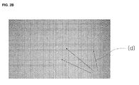
- FIG. 2B is a photograph of a poly-Si layer fabricated when the thermal oxide layer 130 is not formed or has a thickness of less than about 10 ⁇ .
- FIG. 2C is a photograph of a poly-Si layer fabricated when the thermal oxide layer 130 has a thickness of more than 50 ⁇ .
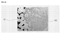
- FIG. 2D is a photograph of a poly-Si layer fabricated when an oxide layer is formed on an a-Si layer using a CVD or PVD technique.
- FIG. 2A shows the poly-Si layer fabricated by the method described above according to FIGS 1A to 1C . That is, when the thermal oxide layer 130 is formed to a thickness of about 10 to 50 ⁇ on the a-Si layer 120 and the a-Si layer 120 is crystallized by an SGS crystallization method, the poly-Si layer is formed as exemplified in FIG. 2A .
- the poly-Si layer includes crystal grains with a size of about 20 ⁇ m. In other words, the interval between seeds is about 20 ⁇ m. Also, it can be confirmed that a seed (a) is present in the center of a crystal grain, a crystal grain boundary (b) is present between adjacent crystal grains, and a crystallized region (c) is present between the seed (a) and the crystal grain boundary (b) in the poly-Si layer fabricated by the SGS crystallization method.
- the seed (a), the crystal grain boundary (b), and the region (c) have different crystallinities. Therefore, in the method of fabricating the poly-Si layer according to the present embodiment, it can be seen that the a-Si layer 120 is crystallized by the SGS crystallization method.
- FIG. 2B shows a poly-Si layer fabricated when the thermal oxide layer 130 is not formed or is formed to a thickness of less than 10 ⁇ on the a-Si layer 120.
- the poly-Si layer formed without forming a thermal layer has the same characteristics as a poly-Si layer obtained by an MIC method.
- FIG. 2C shows a poly-Si layer fabricated when a thermal oxide layer 130 is formed on the a-Si layer 120 to a thickness of about 100 ⁇ , instead of being formed to a thickness of 10 to 50 ⁇ , and the a-Si layer 120 is crystallized.
- the poly-Si layer shown in FIG. 2C includes the region (e) where the SGS crystallization region is mixed with the SPC crystallization region so that an unclear crystal grain boundary is formed.
- FIG. 2D shows the poly-Si layer fabricated when an oxide layer is deposited on the a-Si layer 120 to a thickness of several hundreds of A using a CVD technique and the a-Si layer 120 is crystallized.
- the oxide layer is non-uniformly formed so that metal catalysts are non-uniformly diffused into the a-Si layer 120.
- the poly-Si layer includes not only an SGS crystallization region (f) but also a region (g) where an MIC-type crystallization region is mixed with an SGS crystallization region.
- the thermal oxide layer 130 when the thermal oxide layer 130 is formed to a thickness of about 10 to 50 ⁇ on the a-Si layer 120 and the metal catalyst layer 140 is formed on the thermal oxide layer 130, the a-Si layer 120 may be crystallized by an SGS crystallization method. Also, when the thermal oxide layer 130 is formed during the dehydrogenation of the a-Si layer 120, an additional process of forming a capping layer may be omitted, thereby simplifying the fabrication process of the poly-Si layer.
- FIGs. 3A through 3D are cross-sectional views illustrating a process of fabricating a top-gate TFT using the method of fabricating a poly-Si layer according to FIGS. 1A to 1C .
- the process of fabricating the top-gate TFT will now be described with reference to the method shown in FIGS. 1A through 1C , except for particulars mentioned below.
- a buffer layer 310 is formed on a substrate 300 formed of glass, stainless steel, or plastic. Thereafter, an a-Si layer 320, a thermal oxide layer 330, and a metal catalyst layer 340 are formed on the buffer layer 310 and then annealed (refer to 350) so that the a-Si layer 320 is crystallized into a poly-Si layer 360 by an SGS crystallization method.
- the metal catalyst layer 340 shown in FIG. 3A is removed, and the poly-Si layer 360 and the thermal oxide layer 330 shown in FIG. 3A are patterned.
- the patterned poly-Si layer becomes a semiconductor layer 370 of a TFT as shown in FIG. 3B .
- the poly-Si layer 360 and the thermal oxide layer 330 may be patterned in a subsequent process.
- a gate insulating layer 380 is formed on the entire surface of the substrate 300.
- the gate insulating layer 380 may be a silicon oxide layer, a silicon nitride layer, or a combination thereof.
- the thermal oxide layer 330 is not removed, and the gate insulating layer 380 is formed on the thermal oxide layer 330.
- the thermal oxide layer 330 functions as an insulating layer that electrically insulates the semiconductor layer 370 from a gate electrode that will be formed later.
- the thermal oxide layer 330 has a lower defect density than an oxide layer formed using a CVD technique or a PVD technique and has a uniform film quality.
- the thermal oxide layer 330 when the thermal oxide layer 330 is not removed but is left on the semiconductor layer 370, the insulation of the semiconductor layer 370 from the gate electrode can be further improved.
- the thermal oxide layer 330 may be removed and the gate insulating layer 380 may be formed to contact the semiconductor layer 370.
- a metal layer (not shown) for a gate electrode is formed on the gate insulating layer 380.
- the metal layer may be a single layer formed of an Al alloy such as aluminum-neodymium (Al-Nd), or a combination obtained by stacking an Al alloy on a Cr or Mo alloy.
- Al-Nd aluminum-neodymium
- the metal layer for the gate electrode is etched using photolithography and etching processes, thereby forming a gate electrode 385 corresponding to a channel region of the semiconductor layer 370.
- conductive impurity ions are doped using the gate electrode 385 as a mask, thereby forming a source region 371 and a drain region 372 in the semiconductor layer 370.
- the impurity ions may be p-type ions or n-type ions.
- the p-type ions may be selected from the group consisting of boron (B), aluminum (Al), gallium (Ga), and indium (In), and the n-type ions may be one selected from the group consisting of phosphorus (P), antimony (Sb), and arsenic (As).
- An undoped region interposed between the source region 371 and the drain region 372 functions as a channel region 373.
- the doping process may be performed before the gate electrode 385 is formed using a photo resist.
- an interlayer insulating layer 390 is formed on the entire surface of the substrate 300 including the gate electrode 385.
- the interlayer insulating layer 390 may be a silicon nitride layer, a silicon oxide layer, or a combination thereof.
- the interlayer insulating layer 390, the gate insulating layer 380, and the thermal oxide layer 330 are etched, thereby forming a contact hole exposing the source and drain regions 371 and 372 of the semiconductor layer 370.
- source and drain electrodes 391 and 392 are formed to be respectively connected to the source and drain regions 371 and 372 through contact holes.
- the source and drain electrodes 391 and 392 may be formed of one selected from the group consisting of molybdenum (Mo), chrome (Cr), tungsten (W), aluminum-neodymium (Al-Nd), titanium (Ti), tungsten molybdenum (MoW), and aluminum (Al).
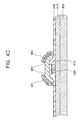
- FIGs. 4A through 4C are cross-sectional views illustrating a process of fabricating a bottom-gate TFT using the method of fabricating a poly-Si layer according to an the embodiment shown in FIGS. 1A through 1C .
- the process of fabricating the bottom-gate TFT will now be described with reference to the method shown in FIGS. 1A through 1C , except for particulars mentioned below.
- a buffer layer 410 is formed on a substrate 400.
- a metal layer (not shown) for a gate electrode is formed on the buffer layer 410 and then, the metal layer is etched using photolithography and etching processes, thereby forming a gate electrode 420. Thereafter, a gate insulating layer 430 is formed on the substrate 400 having the gate electrode 420.
- an a-Si layer 440 is formed on the gate insulating layer 430, and a thermal oxide layer 450 is formed to a thickness of about 10 to 50 ⁇ on the a-Si layer 440.
- a thermal oxide layer 450 is formed during the dehydrogenation of the a-Si layer 440, an additional process of forming a capping layer required for crystallizing the a-Si layer 440 using an SGS crystallization method can be omitted, thereby simplifying the fabrication process.
- a metal catalyst layer 460 is formed on the thermal oxide layer 450 and then annealed so that the a-Si layer 440 is crystallized into a poly-Si layer 470 by an SGS crystallization method.
- the metal catalyst layer 460 and the thermal oxide layer 450 shown in FIG. 4B are removed, and the poly-Si layer 470 is patterned.
- the patterned poly-Si layer becomes a semiconductor layer 475 of a TFT.
- the metal catalyst layer 460 and the thermal oxide layer 450 may be removed after a primary annealing process in which a metal catalyst of the metal catalyst layer 460 moves to an interface between the thermal oxide layer 450 and the a-Si layer 440 to form seeds.
- an ohmic contact material layer and a source/drain conductive layer are sequentially stacked on the semiconductor layer 475.
- the source/drain conductive layer and the ohmic contact material layer are sequentially patterned, thereby forming source and drain electrodes 491 and 492 and an ohmic contact layer 480.
- the ohmic contact layer 480 may be a doped a-Si layer.
- the source/drain conductive layer and the ohmic contact layer may be patterned using a single mask.
- the ohmic contact layer 480 may be disposed under the entire bottom surfaces of the source and drain electrodes 491 and 492.
- the ohmic contact layer 480 is interposed between the semiconductor layer 475 and the source and drain electrodes 491 and 492 so that the source and drain electrodes 491 and 492 can be in ohmic contact with the semiconductor layer 475.
- the ohmic contact layer 480 may be omitted.
- a conductive region may be formed on the semiconductor layer 475 so that the semiconductor layer 475 can be in ohmic contact with the source and drain electrodes 491 and 492.
- the bottom-gate TFT including the gate electrode 420, the semiconductor layer 475, and the source and drain electrodes 491 and 492 is completed.
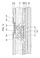
- FIG. 5 is a cross-sectional view of an organic light emitting diode (OLED) display device including a top-gate TFT according to an exemplary embodiment of the present invention.
- OLED organic light emitting diode
- an insulating layer 510 is formed on the entire surface of the substrate 300 including the TFT shown in FIG. 3D .
- the insulating layer 510 may be an inorganic layer or an organic layer.
- the inorganic layer may be one selected from the group consisting of a silicon oxide layer, a silicon nitride layer, and a silicon-on-glass (SOG) layer
- the organic layer may be formed of one selected from the group consisting of polyimide, benzocyclobutene series resin (BCB resin), and acrylate.
- the insulating layer 510 may be a stack structure of the inorganic layer and the organic layer.
- the insulating layer 510 may be etched, thereby forming a via hole exposing one of the source and drain electrodes 391 and 392.
- a first electrode 520 is formed to be connected to one of the source and drain electrodes 391 and 392 through the via hole.
- the first electrode 520 may be formed as an anode or a cathode.
- the anode may be formed using a transparent conductive layer formed of one of indium tin oxide (ITO), indium zinc oxide (IZO), and indium tin zinc oxide (ITZO).
- ITO indium tin oxide
- IZO indium zinc oxide
- ITZO indium tin zinc oxide
- the cathode may be formed of one selected from the group consisting of Mg, Ca, Al, Ag, Ba, and an alloy thereof.
- a pixel defining layer 530 is formed on the first electrode 520 to have an opening exposing a portion of the surface of the first electrode 520, and an organic layer 540 having an emission layer (EML) is formed on the exposed portion of the first electrode 520.
- the organic layer 540 may further include at least one selected from the group consisting of a hole injection layer (HIL), a hole transport layer (HTL), a hole blocking layer (HBL), an electron blocking layer (EBL), an electron injection layer (EIL), and an electron transport layer (ETL).
- HIL hole injection layer
- HTL hole transport layer
- HBL hole blocking layer
- EBL electron blocking layer
- EIL electron injection layer
- ETL electron transport layer
- a thermal oxide layer is formed to a thickness of about 10 to 50 ⁇ on an a-Si layer so that the a-Si layer can be crystallized into a poly-Si layer by an SGS crystallization method.
- the thermal oxide layer may be formed during the dehydrogenation of the a-Si layer so that an additional process of forming a capping layer required for the SGS crystallization method can be omitted, thereby simplifying the fabrication process.
- the thermal oxide layer having a good insulation characteristic may be kept rather than removed and may be used to electrically insulate a semiconductor layer from a gate electrode, thereby improving the insulation characteristic of the semiconductor layer from the gate electrode.
- an a-Si layer can be crystallized into a poly-Si layer by an SGS crystallization method. Also, an additional process of forming a capping layer can be omitted, thereby simplifying the fabrication process of the poly-Si layer.
Abstract
Description
- Aspects of the present invention relate to a method of fabricating a polycrystalline silicon (poly-Si) layer, a thin film transistor (TFT) fabricated using the same, a method of fabricating the TFT, and an organic lighting emitting diode (OLED) display device including the TFT. More particularly, aspects of the present invention relate to a method of fabricating a poly-Si (Polycrystalline Silicon) layer, in which a thermal oxide layer is formed to a thickness of about 10 to 50Å on an amorphous silicon (a-Si) layer so as to crystallize the a-Si layer into a poly-Si layer using a super grain silicon (SGS) crystallization method, a TFT fabricated using the same, a method of fabricating the TFT, and an OLED display device including the TFT. In the method, an additional process of forming a capping layer typically required for the SGS crystallization method may be omitted.
- In general, a polycrystalline silicon (poly-Si) layer is widely used as a semiconductor layer for a thin film transistor (TFT) because the poly-Si has a high field-effect mobility, can be applied to a high-speed operating circuit, and can used to configure a complementary-metal-oxide-semiconductor (CMOS) circuit. A TFT using a poly-Si layer is typically used as an active device of an active-matrix liquid crystal display (AMLCD) or a switching device or a driving device of an organic light emitting diode (OLED).
- Methods of crystallizing an a-Si layer into a poly-Si layer may include a solid phase crystallization (SPC) method, an excimer laser crystallization (ELC) method, a metal induced crystallization (MIC) method, and a metal induced lateral crystallization (MILC) method. In the SPC method, an a-Si layer is annealed for several to several tens of hours at temperatures below 700 °C, the temperature at which the glass substrate typically used in a TFT for a display device is transformed. In the ELC method, excimer laser beams are irradiated onto an a-Si layer so that the a-Si layer is partially heated to a high temperature in a very short amount of time. In the MIC method, a metal such as nickel (Ni), palladium (Pd), gold (Au), or aluminum (Al) is brought into contact with or doped into an a-Si layer to induce a phase change of the a-Si layer into a poly-Si layer. In the MILC method, silicide formed by reaction of metal with silicon laterally diffuses so as to sequentially induce crystallization of an a-Si layer.
- However, the SPC method takes too much time and may lead to deformation of the substrate because the substrate is annealed at a high temperature for a long time. The ELC method requires expensive laser apparatuses and results in the formation of protrusions on the poly-Si surface, thereby degrading interfacial characteristics between a semiconductor layer and a gate insulating layer. When the MIC or MILC method is employed, a large amount of metal catalyst may remain in a crystallized poly-Si layer, thereby increasing leakage current of the semiconductor layer of a TFT.
- Recently, a vast amount of research has been conducted on methods of crystallizing an a-Si layer using a metal catalyst in order to crystallize the a-Si layer at a lower temperature and in a shorter amount of time than in an SPC method. Typical methods of crystallizing an a-Si layer using a metal catalyst are the MIC method and the MILC method mentioned above. In these methods, however, the device characteristics of a TFT may be degraded due to contamination caused by the metal catalyst.
- In order to prevent the contamination caused by the metal catalyst, a super grain silicon (SGS) crystallization method has been developed. In the SGS crystallization method, the amount of metal catalyst that diffuses into the a-Si layer is controlled to provide a low concentration of the metal catalyst in the a-Si layer. Because the metal catalyst is spaced apart at a low concentration in the a-Si layer, the size of crystal grains that are catalyzed by the metal catalyst ranges from several to several hundred µm. Typically, the SGS crystallization method may include forming a capping layer to control diffusion of the metal catalyst into the a-Si layer, forming a metal catalyst layer on the capping layer, and annealing the metal catalyst layer so that a low concentration of the metal catalyst diffuses through the capping layer and into the a-Si layer, and then crystallizing the a-Si layer into a poly-Si layer.
- However, the above-described SGS crystallization method involves an additional process of forming a capping layer, which is typically carried out using a chemical vapor deposition (CVD) technique or a physical vapor deposition (PVD) technique, thereby complicating the fabrication process of the poly-Si layer.
- Aspects of the present invention provide a method of fabricating a polycrystalline silicon (poly-Si) layer, in which a super grain silicon (SGS) crystallization method is performed without an additional process of forming a capping layer, a thin film transistor (TFT) fabricated using the same, a method of fabricating the TFT, and an organic light emitting diode (OLED) display device including the TFT.
- According to an embodiment of the present invention, a method of fabricating a poly-Si layer includes: providing a substrate; forming an amorphous silicon (a-Si) layer on the substrate; forming a thermal oxide layer to a thickness of about 10 to 50Å on the a-Si layer; forming a metal catalyst layer on the thermal oxide layer; and annealing the substrate to crystallize the a-Si layer into the poly-Si layer using a metal catalyst of the metal catalyst layer.
- Preferably the method further comprises the step of dehydrogenating the a-Si layer after forming the a-Si layer. Preferably the thermal oxide layer is formed during the dehydrogenating of the a-Si layer. Preferably the thermal oxide layer is formed by thermally oxidizing a surface portion of the a-Si layer in an atmosphere containing O2 gas or moisture, and an inert gas. Preferably the inert gas includes a N2 gas. Therefore, preferably the thermal oxide layer is formed of SiO2. Preferably the thermal oxide layer is formed at a temperature of about 200 to 1300° C (preferably 400 to 700°C). Preferably the a-Si layer is crystallized by a super grain silicon (SGS) crystallization method using the metal catalyst of the metal catalyst layer. Preferably the metal catalyst of the metal catalyst layer is formed at a concentration of about 1012 to 1014 atoms/cm2.
- According to another embodiment of the present invention, a TFT includes a substrate; a semiconductor layer disposed on the substrate and crystallized using a metal catalyst for crystallization; a thermal oxide layer disposed on the semiconductor layer and having a thickness of about 10 to 50Å; a gate insulating layer disposed on the thermal oxide layer; a gate electrode disposed on the gate insulating layer; an interlayer insulating layer disposed on the gate electrode; and source and drain electrodes disposed on the interlayer insulating layer and electrically connected to source and drain regions of the semiconductor layer.
- Preferably the thermal oxide layer has a thickness of about 17 to 26Å. Preferably the semiconductor layer includes the metal catalyst in a concentration of 1 ×10⁹ to 1 ×10¹³ atoms/cm2 in the semiconductor layer at a distance of about 100Å from a contact surface between the semiconductor layer and the thermal oxide layer. Preferably the semiconductor layer is crystallized by a super grain silicon (SGS) crystallization method.
- According to still another embodiment of the present invention, a method of fabricating a TFT includes: providing a substrate; forming an a-Si layer on the substrate; forming a thermal oxide layer to a thickness of about 10 to 50Å on the a-Si layer; forming a metal catalyst layer for crystallization on the thermal oxide layer; annealing the substrate to crystallize the a-Si layer into a poly-Si layer using a metal catalyst of the metal catalyst layer for crystallization; removing the metal catalyst layer; patterning the thermal oxide layer and patterning the poly-Si layer to form a semiconductor layer; forming a gate insulating layer on the substrate having the semiconductor layer and the thermal oxide layer; forming a gate electrode on the gate insulating layer; forming an interlayer insulating layer on the gate electrode; and forming source and drain electrodes on the interlayer insulating layer to be electrically connected to source and drain regions of the semiconductor layer.
- Preferably the method further comprises the step of dehydrogenating the a-Si layer after forming the a-Si layer. Preferably the thermal oxide layer is formed during the dehydrogenating of the a-Si layer. Preferably the thermal oxide layer is formed by thermally oxidizing a surface portion of the a-Si layer in an atmosphere containing O2 gas or moisture, and inert gas. Preferably the inert gas includes N2 gas. Preferably the thermal oxide layer is formed at a temperature of about 400 to 700°C. Preferably the a-Si layer is crystallized by an SGS crystallization method using the metal catalyst of the metal catalyst layer. Preferably the metal catalyst of the metal catalyst layer for crystallization is formed at a concentration of about 1012 to 1014 atoms/cm2.
- According to yet another aspect of the present invention, an OLED display device includes: a substrate; a semiconductor layer disposed on the substrate and crystallized using a metal catalyst for crystallization; a thermal oxide layer disposed on the semiconductor layer and having a thickness of about 10 to 50Å; a gate insulating layer disposed on the thermal oxide layer; a gate electrode disposed on the gate insulating layer; an interlayer insulating layer disposed on the gate electrode; source and drain electrodes disposed on the interlayer insulating layer and electrically connected to source and drain regions of the semiconductor layer; a first electrode electrically connected to one of the source and drain electrodes; an organic layer disposed on the first electrode and including an emission layer (EML); and a second electrode disposed on the organic layer.
- Preferably the thermal oxide layer has a thickness of about 17 to 26Å. Preferably the metal catalyst for crystallization is formed at a concentration of 1×10⁹ to 1×10¹³ atoms/cm2 in the semiconductor layer at a distance of about 100Å from a contact surface between the semiconductor layer and the thermal oxide layer toward the substrate. Preferably the semiconductor layer is crystallized by an SGS crystallization method.
- Additional aspects and/or advantages of the invention will be set forth in part in the description which follows and, in part, will be obvious from the description, or may be learned by practice of the invention.
- These and/or other aspects of the invention will become apparent and more readily appreciated from the following description of the embodiments, taken in conjunction with the accompanying drawings of which:
-
FIG. 1A through 1C are cross-sectional views illustrating a process of fabricating a polycrystalline silicon (poly-Si) layer using a super grain silicon (SGS) crystallization method according to an embodiment of the present invention; -
FIG. 2A is a photographic representation of a poly-Si layer crystallized using a method according the embodiment ofFIGS. 1A through 1C ; -
FIG. 2B is a photographic representation of a poly-Si layer fabricated when the thermal oxide layer is not formed or has a thickness of less than about 10Å; -
FIG. 2C is a photographic representation of a poly-Si layer fabricated when the thermal oxide layer has a thickness of more than 50Å; -
FIG. 2D is a photographic image of a poly-Si layer fabricated when an oxide layer of several hundreds of angstroms is formed on an a-Si layer using a chemical vapor deposition (CVD) technique; -
FIGs. 3A through 3D are cross-sectional views illustrating a process of fabricating a top-gate thin film transistor (TFT) using a method of fabricating a poly-Si layer according toFIGS. 1A through 1C ; -
FIGs. 4A through 4C are cross-sectional views illustrating a process of fabricating a bottom-gate TFT using a method of fabricating a poly-Si layer according toFIGS. 1A through 1C ; and -
FIG. 5 is a cross-sectional view of an organic light emitting diode (OLED) display device including a top-gate TFT according to an embodiment of the present invention. - Reference will now be made in detail to the present embodiments of the present invention, examples of which are illustrated in the accompanying drawings, wherein like reference numerals refer to the like elements throughout. The embodiments are described below in order to explain the present invention by referring to the figures.
-
FIGs. 1A through 1C are cross-sectional views illustrating a process of forming a polycrystalline silicon (poly-Si) layer using a super grain silicon (SGS) crystallization method according to an embodiment of the present invention. - Referring to
FIG. 1A , asubstrate 100 is prepared. Thesubstrate 100 may be formed of glass, stainless steel, or plastic. Abuffer layer 110 is formed on thesubstrate 100 using a chemical vapor deposition (CVD) technique or a physical vapor deposition (PVD) technique. Thebuffer layer 110 may be a single layer or multiple insulating layers of silicon oxide layer and/or silicon nitride. Thebuffer layer 110 prevents the diffusion of moisture or impurities generated in thesubstrate 100 and/or controls the transmission rate of heat during a crystallization process, thereby facilitating the crystallization of the amorphous silicon (a-Si) layer. - Thereafter, an
a-Si layer 120 is formed on thebuffer layer 110. Typically, thea-Si layer 120 is formed using a CVD technique. Thea-Si layer 120 formed using a CVD technique may contain a gas such as H2 gas, in which can cause problems such as a reduction in electron mobility. Therefore, a dehydrogenation process may be performed such that H2 does not remain in thea-Si layer 120. - Thereafter, a
thermal oxide layer 130 is formed to a thickness of about 10 to 50 Å on thea-Si layer 120. Thethermal oxide layer 130 may be obtained by thermally oxidizing thea-Si layer 120 in an atmosphere containing O2 gas or moisture, and an inert gas. As a non-limiting example, the thermal oxidation may be performed at a temperature of about 400 to 700°C. It is difficult to cause thermal oxidation at temperatures Below 400°C, it may be difficult to achieve thermal oxidation; on the other hand, above 700°C, the substrate may become deformed during the thermal oxidation. The inert gas may be N2 gas or Ar gas. When thethermal oxide layer 130 is formed in an N2 atmosphere, thethermal oxide layer 130 may become densified. - As described above, the
thermal oxide layer 130 may be formed to a thickness of about 10 to 50Å. When thethermal oxide layer 130 has a thickness of less than about 10Å, thethermal oxide layer 130 may not properly function as a capping layer to control the concentration of the metal catalyst that diffuses into thea-Si layer 120. As a result, crystallization of thea-Si layer 120 may be caused not by an SGS crystallization method but by an MIC method, resulting in smaller grains and possible contamination from excess metal catalyst in the formed poly-Si layer. On the other hand, if thethermal oxide layer 130 has a thickness of more than about 50Å, only a small amount of metal catalyst diffuses into thea-Si layer 120, thereby reducing the number of crystal nuclei (or seeds). As a result, thea-Si layer 120 may be incompletely crystallized. - More specifically, the
thermal oxide layer 130 may be formed to a thickness of about 17 to 26 Å. In this case, when thea-Si layer 120 is crystallized by diffusing the metal catalyst through thethermal oxide layer 130, thea-Si layer 120 may be completely crystallized by an SGS crystallization method, and the metal catalyst remaining in the crystallized poly-Si layer may be controlled to have a low concentration. - In general, when an oxide layer is separately formed by a CVD method or a PVD method, it is difficult in terms of processibility to form the oxide layer to a thickness of several tens of A or less. Accordingly, the oxide layer must be formed to a thickness of several hundreds of A in consideration of mass production. In this case, the oxide layer cannot have a uniform film quality as compared with the
thermal oxide layer 130. Therefore, when the oxide layer is used as a capping layer for an SGS crystallization method, a metal catalyst for crystallization may be non-uniformly diffused into thea-Si layer 120. Thus, due to the great thickness of the oxide layer, the metal catalyst may not diffuse into thea-Si layer 120 or a region where the metal catalyst is not diffused to such a concentration as to form seeds may be formed. As a result, thea-Si layer 120 may not be uniformly crystallized during the SGS crystallization process. - By comparison, the
thermal oxide layer 130, which is formed by thermally oxidizing thea-Si layer 120, has more uniform film quality than the oxide layer formed using a CVD technique or a PVD technique. Therefore, by the use of thethermal oxide layer 130, a metal catalyst for crystallization may be uniformly diffused into thea-Si layer 120. Also, since thethermal oxide layer 130 may be formed to a small thickness of about 10 to 50Å, the metal catalyst may be diffused such that thea-Si layer 120 is completely crystallized by an SGS crystallization method. - Furthermore, the
thermal oxide layer 130 may be formed at the same time as the dehydrogenation of thea-Si layer 120. In this case, an additional process of forming a capping layer may be omitted, thereby further simplifying the SGS crystallization process. - Referring to
FIG. 1B , a metal catalyst is deposited on thethermal oxide layer 130, thereby forming ametal catalyst layer 140. As non-limiting examples, the metal catalyst may be one selected from the group consisting of Ni, Pd, Ti, Ag, Au, Al, Sn, Sb, Cu, Co, Mo, Tr, Ru, Rh, Cd, and Pt. As a specific example, the metal catalyst may be Ni. Themetal catalyst layer 140 may be formed to an areal density of about 1011 to 1015 atoms/cm2 on thethermal oxide layer 130. When themetal catalyst layer 140 is formed to an areal density lower than about 1011 atoms/cm2, only a small number of seeds are formed, thereby reducing the likelihood of crystallization of thea-Si layer 120 into a poly-Si layer. When themetal catalyst layer 140 is formed to an areal density of more than about 1015 atoms/cm2, the amount of the metal catalyst diffusing into thea-Si layer 120 is increased, thereby causing an MIC process rather than the SGS crystallization process. Also, the amount of the remaining metal catalyst is increased so that the characteristic of a semiconductor layer formed by patterning the poly-Si layer may be degraded. - Referring to
FIG. 1C , thesubstrate 100 including thebuffer layer 110, thea-Si layer 120, thethermal oxide layer 130, and themetal catalyst layer 140 is annealed (refer to 150) so that thea-Si layer 120 is crystallized using an SGS crystallization method. During theannealing process 150, only a small amount ofmetal catalyst 140b out of themetal catalysts thermal oxide layer 130 reaches the surface of thea-Si layer 120, whereas a large amount of themetal catalyst 140a neither reaches thea-Si layer 120 nor passes through thethermal oxide layer 130. - The
metal catalyst 140b that passes through thethermal oxide layer 130 and diffuses into the surface of thea-Si layer 120 catalyzes the crystallizing of thea-Si layer 120 into a poly-Si layer 160. That is, the diffusedmetal catalyst 140b combines with Si of thea-Si layer 120 to form a metal silicide. The metal silicide forms seeds, thereby crystallizing thea-Si layer 120 into the poly-Si layer 160. Theannealing process 150 may be performed using any one of a furnace process, a rapid thermal annealing (RTA) process, a ultraviolet (UV) process, and a laser process. - The
annealing process 150 may be performed twice. Specifically, a primary annealing process includes moving the metal catalyst of themetal catalyst layer 140 to an interface between thethermal oxide layer 130 and thea-Si layer 120 to form seeds. A secondary annealing process includes crystallizing thea-Si layer 120 into the poly-Si layer 160 using the seeds. In this case, the primary annealing process may be performed at a temperature of about 200 to 800°C, and the secondary annealing process may be performed at a temperature of about 400 to 1300°C. - As illustrated in
FIG. 1C , theannealing process 150 may be performed without removing themetal catalyst layer 140. However, as an alternative, themetal catalyst layer 140 may be removed after the primary annealing process so that additional diffusion or penetration of the metal catalyst can be prevented during the secondary annealing process. - In the poly-
Si layer 160 obtained by crystallizing thea-Si layer 120 through the SGS crystallization method using thethermal oxide layer 130 and themetal catalyst layer 140, a metal catalyst is formed at a concentration of 1×10⁹ to 1×10¹³ atoms/cm2 at a distance of about 100Å from the top surface of the poly-Si layer 160 (i.e., from a contact surface between the poly-Si layer 160 and the thermal oxide layer 130) toward thesubstrate 100. -
FIG. 2A is a photograph of a poly-Si layer crystallized by the method according toFIGS. 1A to 1C .FIG. 2B is a photograph of a poly-Si layer fabricated when thethermal oxide layer 130 is not formed or has a thickness of less than about 10Å.FIG. 2C is a photograph of a poly-Si layer fabricated when thethermal oxide layer 130 has a thickness of more than 50Å.FIG. 2D is a photograph of a poly-Si layer fabricated when an oxide layer is formed on an a-Si layer using a CVD or PVD technique. -
FIG. 2A shows the poly-Si layer fabricated by the method described above according toFIGS 1A to 1C . That is, when thethermal oxide layer 130 is formed to a thickness of about 10 to 50Å on thea-Si layer 120 and thea-Si layer 120 is crystallized by an SGS crystallization method, the poly-Si layer is formed as exemplified inFIG. 2A . - Referring to
FIG. 2A , the poly-Si layer includes crystal grains with a size of about 20µm. In other words, the interval between seeds is about 20µm. Also, it can be confirmed that a seed (a) is present in the center of a crystal grain, a crystal grain boundary (b) is present between adjacent crystal grains, and a crystallized region (c) is present between the seed (a) and the crystal grain boundary (b) in the poly-Si layer fabricated by the SGS crystallization method. The seed (a), the crystal grain boundary (b), and the region (c) have different crystallinities. Therefore, in the method of fabricating the poly-Si layer according to the present embodiment, it can be seen that thea-Si layer 120 is crystallized by the SGS crystallization method. - As a comparative example,
FIG. 2B shows a poly-Si layer fabricated when thethermal oxide layer 130 is not formed or is formed to a thickness of less than 10Å on thea-Si layer 120. - Referring to
FIG. 2B , a crystal grain boundary cannot be confirmed in the poly-Si layer, and it can be observed that metal silicide conglomerates (d) are uniformly distributed in the poly-Si layer. Accordingly, it can be seen that the poly-Si layer formed without forming a thermal layer has the same characteristics as a poly-Si layer obtained by an MIC method. - As another comparative example,
FIG. 2C shows a poly-Si layer fabricated when athermal oxide layer 130 is formed on thea-Si layer 120 to a thickness of about 100Å, instead of being formed to a thickness of 10 to 50Å, and thea-Si layer 120 is crystallized. - Referring to
FIG. 2C , since only a small amount of metal catalyst diffuses into thea-Si layer 120, the number of seeds is reduced. As a result, thea-Si layer 120 is incompletely crystallized, and a region (e) exists where an SGS crystallization region is mixed with an SPC crystallization region(that is, a region that is crystallized by heat only). As compared with the poly-Si layer shown inFIG. 2A , which is completely crystallized by the SGS crystallization method, the poly-Si layer shown inFIG. 2C includes the region (e) where the SGS crystallization region is mixed with the SPC crystallization region so that an unclear crystal grain boundary is formed. - As still another comparative example,
FIG. 2D shows the poly-Si layer fabricated when an oxide layer is deposited on thea-Si layer 120 to a thickness of several hundreds of A using a CVD technique and thea-Si layer 120 is crystallized. - Referring to
FIG. 2D , the oxide layer is non-uniformly formed so that metal catalysts are non-uniformly diffused into thea-Si layer 120. Thus, the poly-Si layer includes not only an SGS crystallization region (f) but also a region (g) where an MIC-type crystallization region is mixed with an SGS crystallization region. - Therefore, according to aspects of the present invention, it can be seen that when the
thermal oxide layer 130 is formed to a thickness of about 10 to 50Å on thea-Si layer 120 and themetal catalyst layer 140 is formed on thethermal oxide layer 130, thea-Si layer 120 may be crystallized by an SGS crystallization method. Also, when thethermal oxide layer 130 is formed during the dehydrogenation of thea-Si layer 120, an additional process of forming a capping layer may be omitted, thereby simplifying the fabrication process of the poly-Si layer. -
FIGs. 3A through 3D are cross-sectional views illustrating a process of fabricating a top-gate TFT using the method of fabricating a poly-Si layer according toFIGS. 1A to 1C . The process of fabricating the top-gate TFT will now be described with reference to the method shown inFIGS. 1A through 1C , except for particulars mentioned below. - Referring to
FIG. 3A , abuffer layer 310 is formed on asubstrate 300 formed of glass, stainless steel, or plastic. Thereafter, ana-Si layer 320, athermal oxide layer 330, and ametal catalyst layer 340 are formed on thebuffer layer 310 and then annealed (refer to 350) so that thea-Si layer 320 is crystallized into a poly-Si layer 360 by an SGS crystallization method. - Referring to
FIG. 3B , themetal catalyst layer 340 shown inFIG. 3A is removed, and the poly-Si layer 360 and thethermal oxide layer 330 shown inFIG. 3A are patterned. The patterned poly-Si layer becomes asemiconductor layer 370 of a TFT as shown inFIG. 3B . Alternatively, the poly-Si layer 360 and thethermal oxide layer 330 may be patterned in a subsequent process. - Thereafter, a
gate insulating layer 380 is formed on the entire surface of thesubstrate 300. Thegate insulating layer 380 may be a silicon oxide layer, a silicon nitride layer, or a combination thereof. In the current embodiment, thethermal oxide layer 330 is not removed, and thegate insulating layer 380 is formed on thethermal oxide layer 330. In this case, thethermal oxide layer 330 functions as an insulating layer that electrically insulates thesemiconductor layer 370 from a gate electrode that will be formed later. Thethermal oxide layer 330 has a lower defect density than an oxide layer formed using a CVD technique or a PVD technique and has a uniform film quality. Therefore, when thethermal oxide layer 330 is not removed but is left on thesemiconductor layer 370, the insulation of thesemiconductor layer 370 from the gate electrode can be further improved. Alternatively, thethermal oxide layer 330 may be removed and thegate insulating layer 380 may be formed to contact thesemiconductor layer 370. - Subsequently, a metal layer (not shown) for a gate electrode is formed on the
gate insulating layer 380. The metal layer may be a single layer formed of an Al alloy such as aluminum-neodymium (Al-Nd), or a combination obtained by stacking an Al alloy on a Cr or Mo alloy. The metal layer for the gate electrode is etched using photolithography and etching processes, thereby forming agate electrode 385 corresponding to a channel region of thesemiconductor layer 370. - Referring to
FIG. 3C , conductive impurity ions are doped using thegate electrode 385 as a mask, thereby forming asource region 371 and adrain region 372 in thesemiconductor layer 370. The impurity ions may be p-type ions or n-type ions. The p-type ions may be selected from the group consisting of boron (B), aluminum (Al), gallium (Ga), and indium (In), and the n-type ions may be one selected from the group consisting of phosphorus (P), antimony (Sb), and arsenic (As). An undoped region interposed between thesource region 371 and thedrain region 372 functions as achannel region 373. As an alternative to carrying out the using of the formed gate electrode as a mask, the doping process may be performed before thegate electrode 385 is formed using a photo resist. - Referring to
FIG. 3D , aninterlayer insulating layer 390 is formed on the entire surface of thesubstrate 300 including thegate electrode 385. The interlayer insulatinglayer 390 may be a silicon nitride layer, a silicon oxide layer, or a combination thereof. - Thereafter, the
interlayer insulating layer 390, thegate insulating layer 380, and thethermal oxide layer 330 are etched, thereby forming a contact hole exposing the source and drainregions semiconductor layer 370. After that, source and drainelectrodes regions electrodes semiconductor layer 370, thegate electrode 385, and the source and drainelectrodes -
FIGs. 4A through 4C are cross-sectional views illustrating a process of fabricating a bottom-gate TFT using the method of fabricating a poly-Si layer according to an the embodiment shown inFIGS. 1A through 1C . The process of fabricating the bottom-gate TFT will now be described with reference to the method shown inFIGS. 1A through 1C , except for particulars mentioned below. - Referring to
FIG. 4A , abuffer layer 410 is formed on asubstrate 400. A metal layer (not shown) for a gate electrode is formed on thebuffer layer 410 and then, the metal layer is etched using photolithography and etching processes, thereby forming agate electrode 420. Thereafter, agate insulating layer 430 is formed on thesubstrate 400 having thegate electrode 420. - Referring to
FIG. 4B , ana-Si layer 440 is formed on thegate insulating layer 430, and athermal oxide layer 450 is formed to a thickness of about 10 to 50Å on thea-Si layer 440. When thethermal oxide layer 450 is formed during the dehydrogenation of thea-Si layer 440, an additional process of forming a capping layer required for crystallizing thea-Si layer 440 using an SGS crystallization method can be omitted, thereby simplifying the fabrication process. - A
metal catalyst layer 460 is formed on thethermal oxide layer 450 and then annealed so that thea-Si layer 440 is crystallized into a poly-Si layer 470 by an SGS crystallization method. - Referring to
FIG. 4C , themetal catalyst layer 460 and thethermal oxide layer 450 shown inFIG. 4B are removed, and the poly-Si layer 470 is patterned. The patterned poly-Si layer becomes asemiconductor layer 475 of a TFT. Alternatively, themetal catalyst layer 460 and thethermal oxide layer 450 may be removed after a primary annealing process in which a metal catalyst of themetal catalyst layer 460 moves to an interface between thethermal oxide layer 450 and thea-Si layer 440 to form seeds. - Thereafter, an ohmic contact material layer and a source/drain conductive layer are sequentially stacked on the
semiconductor layer 475. The source/drain conductive layer and the ohmic contact material layer are sequentially patterned, thereby forming source and drainelectrodes ohmic contact layer 480. Theohmic contact layer 480 may be a doped a-Si layer. - In order to reduce the number of masks used in forming the TFT, the source/drain conductive layer and the ohmic contact layer may be patterned using a single mask. In this case, the
ohmic contact layer 480 may be disposed under the entire bottom surfaces of the source and drainelectrodes ohmic contact layer 480 is interposed between thesemiconductor layer 475 and the source and drainelectrodes electrodes semiconductor layer 475. Alternatively, theohmic contact layer 480 may be omitted. In this case, before the source/drain conductive layer is stacked, a conductive region may be formed on thesemiconductor layer 475 so that thesemiconductor layer 475 can be in ohmic contact with the source and drainelectrodes gate electrode 420, thesemiconductor layer 475, and the source and drainelectrodes -
FIG. 5 is a cross-sectional view of an organic light emitting diode (OLED) display device including a top-gate TFT according to an exemplary embodiment of the present invention. - Referring to
FIG. 5 , an insulatinglayer 510 is formed on the entire surface of thesubstrate 300 including the TFT shown inFIG. 3D . The insulatinglayer 510 may be an inorganic layer or an organic layer. The inorganic layer may be one selected from the group consisting of a silicon oxide layer, a silicon nitride layer, and a silicon-on-glass (SOG) layer, and the organic layer may be formed of one selected from the group consisting of polyimide, benzocyclobutene series resin (BCB resin), and acrylate. Also, the insulatinglayer 510 may be a stack structure of the inorganic layer and the organic layer. - The insulating
layer 510 may be etched, thereby forming a via hole exposing one of the source and drainelectrodes first electrode 520 is formed to be connected to one of the source and drainelectrodes first electrode 520 may be formed as an anode or a cathode. When thefirst electrode 520 is an anode, the anode may be formed using a transparent conductive layer formed of one of indium tin oxide (ITO), indium zinc oxide (IZO), and indium tin zinc oxide (ITZO). When thefirst electrode 520 is a cathode, the cathode may be formed of one selected from the group consisting of Mg, Ca, Al, Ag, Ba, and an alloy thereof. - Thereafter, a pixel defining layer 530 is formed on the
first electrode 520 to have an opening exposing a portion of the surface of thefirst electrode 520, and anorganic layer 540 having an emission layer (EML) is formed on the exposed portion of thefirst electrode 520. Theorganic layer 540 may further include at least one selected from the group consisting of a hole injection layer (HIL), a hole transport layer (HTL), a hole blocking layer (HBL), an electron blocking layer (EBL), an electron injection layer (EIL), and an electron transport layer (ETL). Subsequently, asecond electrode 550 is formed on theorganic layer 540. Thus, an OLED display device according to the present embodiment is completed. - Therefore, a thermal oxide layer is formed to a thickness of about 10 to 50Å on an a-Si layer so that the a-Si layer can be crystallized into a poly-Si layer by an SGS crystallization method. Also, the thermal oxide layer may be formed during the dehydrogenation of the a-Si layer so that an additional process of forming a capping layer required for the SGS crystallization method can be omitted, thereby simplifying the fabrication process. Furthermore, the thermal oxide layer having a good insulation characteristic may be kept rather than removed and may be used to electrically insulate a semiconductor layer from a gate electrode, thereby improving the insulation characteristic of the semiconductor layer from the gate electrode.
- According to aspects of the present invention as described above, an a-Si layer can be crystallized into a poly-Si layer by an SGS crystallization method. Also, an additional process of forming a capping layer can be omitted, thereby simplifying the fabrication process of the poly-Si layer.
- Although a few embodiments of the present invention have been shown and described, it would be appreciated by those skilled in the art that changes may be made in this embodiment without departing from the principle of the invention, the scope of which is defined in the claims and their equivalents.
Claims (16)
- A method of fabricating a polycrystalline silicon (poly-Si) layer, comprising:providing a substrate (100, 300);forming an amorphous silicon (a-Si) layer (120, 320) on the substrate (100, 300);forming a thermal oxide layer (130, 330) to a thickness of 10 to 50Å on the a-Si layer (120, 320) by thermally oxidizing at least a surface portion of the a-Si layer (120, 320);forming a metal catalyst layer (140, 340) on the thermal oxide layer (130, 330); andannealing the substrate to crystallize the a-Si layer (120, 320) into a poly-Si layer (160, 360) using a metal catalyst of the metal catalyst layer (140, 340).
- The method according to claim 1, further comprising the step of dehydrogenating the a-Si layer (120, 320) after forming the a-Si layer (120, 320).
- The method according to claim 2, wherein the thermal oxide layer (130, 330) is formed during the dehydrogenating of the a-Si layer (120, 320).
- The method according to one of the preceding claims, wherein the thermal oxide layer (130, 330) is formed by thermally oxidizing a surface portion of the a-Si layer (120, 320) in an atmosphere containing O2 gas or moisture, and an inert gas.
- The method according to claim 4, wherein the inert gas includes N2 gas.
- The method according to one of the preceding claims, wherein the thermal oxide layer (130, 330) is formed at a temperature of 400 to 700°C.
- The method according to one of the preceding claims, wherein the a-Si layer (120, 320) is crystallized by a super grain silicon (SGS) crystallization method using the metal catalyst of the metal catalyst layer.
- The method according to one of the preceding claims, wherein the metal catalyst of the metal catalyst layer (140, 340) is formed at a concentration of about 1012 to 1014 atoms/cm2.
- The method according to one of the preceding claims, wherein the thermal oxide layer (130, 330) is formed with a thickness between 17 to 26Å.
- A method of fabricating a thin film transistor (TFT), comprising:fabricating a polycrystalline silicon (poly-Si) layer (160, 360) by using the method as defined in one of claims 1-9; andremoving the metal catalyst layer (340);patterning the thermal oxide layer (330) and patterning the poly-Si layer (360) to form a semiconductor layer (370);forming a gate insulating layer (380) on the substrate having the semiconductor layer (370) and the thermal oxide layer (330);forming a gate electrode (385) on the gate insulating layer (380);forming an interlayer insulating layer (390) on the gate electrode (385); andforming source and drain electrodes (391, 392) on the interlayer insulating layer (390) to be electrically connected to source and drain regions of the semiconductor layer (370).
- A thin film transistor (TFT) comprising:a substrate (300);a semiconductor layer (370) disposed on the substrate (300) and crystallized using a metal catalyst;a thermal oxide layer (330) disposed on the semiconductor layer (370) and having a thickness of 10 to 50Å;a gate insulating layer (380) disposed on the thermal oxide layer (330);a gate electrode (385) disposed on the gate insulating layer (380);an interlayer insulating layer (390) disposed on the gate electrode (385); andsource and drain electrodes (391, 392) disposed on the interlayer insulating layer (390) and electrically connected to source and drain regions of the semiconductor layer (370).
- The TFT according to claim 11, wherein the thermal oxide layer (330) has a thickness of 17 to 26Å.
- The TFT according to one of claims 11 and 12, wherein thermal oxide layer (330) is formed of SiO2.
- The TFT according to one of claims 11 - 13, wherein the semiconductor layer (370) includes the metal catalyst in a concentration of 1×10⁹ to 1×10¹³ atoms/cm2 in the semiconductor layer (370) at a distance of 100Å from a contact surface between the semiconductor layer (370) and the thermal oxide layer (330).
- The TFT according to claim 11, wherein the semiconductor layer is crystallized by a super grain silicon (SGS) crystallization method.
- An organic light emitting diode (OLED) display device comprising:a TFT according to one of claims 11-15,a first electrode (520) electrically connected to one of the source and drain electrodes (391, 392);an organic layer (540) disposed on the first electrode (520) and including an emission layer (EML); anda second electrode (550) disposed on the organic layer (540).
Applications Claiming Priority (1)
| Application Number | Priority Date | Filing Date | Title |
|---|---|---|---|
| KR1020070059968A KR20080111693A (en) | 2007-06-19 | 2007-06-19 | Fabricating method of polycrystalline silicon, tft fabricated using the same, fabricating method of the tft, and organic lighting emitting diode(oled) display device comprising the same |
Publications (2)
| Publication Number | Publication Date |
|---|---|
| EP2006903A2 true EP2006903A2 (en) | 2008-12-24 |
| EP2006903A3 EP2006903A3 (en) | 2008-12-31 |
Family
ID=39682502
Family Applications (1)
| Application Number | Title | Priority Date | Filing Date |
|---|---|---|---|
| EP08158539A Withdrawn EP2006903A3 (en) | 2007-06-19 | 2008-06-19 | Method of fabricating polycrystalline silicon, TFT fabricated using the same, method of fabricating the TFT, and organic light emitting diode display device including the TFT |
Country Status (6)
| Country | Link |
|---|---|
| US (2) | US7825476B2 (en) |
| EP (1) | EP2006903A3 (en) |
| JP (1) | JP2009004770A (en) |
| KR (1) | KR20080111693A (en) |
| CN (1) | CN101330004A (en) |
| TW (1) | TWI382471B (en) |
Cited By (3)
| Publication number | Priority date | Publication date | Assignee | Title |
|---|---|---|---|---|
| EP2613346A1 (en) * | 2011-11-11 | 2013-07-10 | Boe Technology Group Co. Ltd. | Thin film transistor, manufacturing method thereof and display device |
| WO2013184526A1 (en) * | 2012-06-03 | 2013-12-12 | Silicon Solar Solutions | Ultra-large grain polycrystalline semiconductors through top-down aluminum induced crystallization (taic) |
| TWI492314B (en) * | 2009-11-20 | 2015-07-11 | Semiconductor Energy Lab | Method for manufacturing semiconductor device |
Families Citing this family (29)
| Publication number | Priority date | Publication date | Assignee | Title |
|---|---|---|---|---|
| KR20080111693A (en) * | 2007-06-19 | 2008-12-24 | 삼성모바일디스플레이주식회사 | Fabricating method of polycrystalline silicon, tft fabricated using the same, fabricating method of the tft, and organic lighting emitting diode(oled) display device comprising the same |
| KR100965260B1 (en) * | 2008-01-25 | 2010-06-22 | 삼성모바일디스플레이주식회사 | Thin film transistor, fabricating method for the same, and organic light emitting diode display device comprising the same |
| KR101408962B1 (en) * | 2008-07-01 | 2014-06-17 | 삼성디스플레이 주식회사 | Method of manufacturing transistor and method of manufacturing organic electroluminescence display using the same |
| KR100965259B1 (en) * | 2008-12-18 | 2010-06-22 | 삼성모바일디스플레이주식회사 | Organic light emitting display device and the fabricating method of the same |
| KR101088457B1 (en) * | 2009-04-07 | 2011-12-01 | 주식회사 테라세미콘 | Method For Fabricating Polysilicon Hard Mask Using Metal Catalyst and Method For Fabricating Semiconductor Device Using The Same |
| KR101011806B1 (en) | 2009-04-30 | 2011-02-07 | 노코드 주식회사 | Manufacturing method for thin film of poly-crystalline silicon |
| KR101147414B1 (en) * | 2009-09-22 | 2012-05-22 | 삼성모바일디스플레이주식회사 | Organic light emitting diode display and method for manufacturing the same |
| CN101807545B (en) * | 2010-03-22 | 2013-04-24 | 中国科学院上海微系统与信息技术研究所 | Diode and producing method of resistance converting storage |
| CN102254797A (en) * | 2010-05-18 | 2011-11-23 | 京东方科技集团股份有限公司 | Low-temperature polysilicon membrane and manufacturing method thereof, transistor and display device |
| KR20130077839A (en) * | 2010-05-21 | 2013-07-09 | 가부시키가이샤 한도오따이 에네루기 켄큐쇼 | Semiconductor device and method of manufacturing the same |
| KR101733196B1 (en) | 2010-09-03 | 2017-05-25 | 삼성디스플레이 주식회사 | Thin film transistor and method for manufacturing the same and display divce using the same |
| KR101809661B1 (en) * | 2011-06-03 | 2017-12-18 | 삼성디스플레이 주식회사 | Thin film transistor, manufacturing method of thin film transistor, and organic light emitting diode display including the same |
| KR101860859B1 (en) * | 2011-06-13 | 2018-05-25 | 삼성디스플레이 주식회사 | Manufacturing method of thin film transistor, the thin film transistor manufactured by the same, manufacturing method of organic light emitting apparatus and the organic light emitting apparatus manufactured by the same |
| KR20130007283A (en) * | 2011-06-30 | 2013-01-18 | 삼성디스플레이 주식회사 | Thin flim transistor and organic light emitting diode display using the same and method for manufacturing the sames |
| KR101244298B1 (en) * | 2011-07-13 | 2013-03-18 | 광주과학기술원 | Method of manufacturing Light Emitting Diode using Heat Treatment and Light Emitting Diode of formed by using the same |
| WO2013047629A1 (en) | 2011-09-29 | 2013-04-04 | Semiconductor Energy Laboratory Co., Ltd. | Semiconductor device |
| JP6082562B2 (en) * | 2011-10-27 | 2017-02-15 | 株式会社半導体エネルギー研究所 | Semiconductor device |
| US9123673B2 (en) * | 2013-03-12 | 2015-09-01 | Taiwan Semiconductor Manufacturing Company, Ltd. | Wafer back side processing structure and apparatus |
| CN103311105A (en) * | 2013-05-16 | 2013-09-18 | 上海大学 | Method for inducing crystallization of amorphous silicon thin film into polycrystalline silicon thin film by aluminum at low temperature |
| US9166181B2 (en) | 2014-02-19 | 2015-10-20 | International Business Machines Corporation | Hybrid junction field-effect transistor and active matrix structure |
| CN104538350A (en) * | 2014-12-30 | 2015-04-22 | 深圳市华星光电技术有限公司 | Polycrystalline silicon substrate and manufacturing method thereof |
| CN104465371A (en) * | 2014-12-31 | 2015-03-25 | 深圳市华星光电技术有限公司 | Excimer laser annealing pretreatment method, thin film transistor and production method of thin film transistor |
| KR20170001827A (en) * | 2015-06-25 | 2017-01-05 | 삼성디스플레이 주식회사 | Organic light emitting diode display |
| CN105140180B (en) * | 2015-08-24 | 2018-03-13 | 武汉华星光电技术有限公司 | The preparation method of thin-film transistor array base-plate and the preparation method of polycrystalline silicon material |
| CN105470312A (en) | 2016-02-19 | 2016-04-06 | 深圳市华星光电技术有限公司 | Low-temperature polycrystalline silicon thin film transistor and manufacturing method thereof |
| US11063095B2 (en) | 2017-06-01 | 2021-07-13 | Boe Technology Group Co., Ltd. | Array substrate, display panel having the same, and method of fabricating array substrate |
| KR102596210B1 (en) * | 2018-05-25 | 2023-10-30 | 엘지디스플레이 주식회사 | TFT substrate and display device including the same |
| KR102639769B1 (en) * | 2018-11-22 | 2024-02-26 | 삼성디스플레이 주식회사 | Display apparatus and method of manufacturing the same |
| US11842937B2 (en) | 2021-07-30 | 2023-12-12 | Wolfspeed, Inc. | Encapsulation stack for improved humidity performance and related fabrication methods |
Citations (8)
| Publication number | Priority date | Publication date | Assignee | Title |
|---|---|---|---|---|
| EP0651431A2 (en) * | 1993-10-29 | 1995-05-03 | Semiconductor Energy Laboratory Co., Ltd. | Method of crystallizing a silicone layer and semiconductor devices obtained by using the method |
| US5840600A (en) * | 1994-08-31 | 1998-11-24 | Semiconductor Energy Laboratory Co., Ltd. | Method for producing semiconductor device and apparatus for treating semiconductor device |
| US6162667A (en) * | 1994-03-28 | 2000-12-19 | Sharp Kabushiki Kaisha | Method for fabricating thin film transistors |
| US6346437B1 (en) * | 1998-07-16 | 2002-02-12 | Sharp Laboratories Of America, Inc. | Single crystal TFT from continuous transition metal delivery method |
| US20030034940A1 (en) * | 1996-12-09 | 2003-02-20 | Semiconductor Energy Laboratory Co., Ltd., Japanese Corporation | Active matrix display device and method of manufacturing same |
| US20060030085A1 (en) * | 2004-08-04 | 2006-02-09 | Hye-Hyang Park | Method of fabricating thin film transistor |
| US20060033106A1 (en) * | 2004-08-13 | 2006-02-16 | Jin-Wook Seo | Thin film transistor and method of fabricating the same |
| US20060033107A1 (en) * | 2004-08-13 | 2006-02-16 | Lee Keun-Soo | Thin film transistor and method of fabricating the same |
Family Cites Families (21)
| Publication number | Priority date | Publication date | Assignee | Title |
|---|---|---|---|---|
| JPH0794756A (en) * | 1993-07-27 | 1995-04-07 | Semiconductor Energy Lab Co Ltd | Method of fabricating semiconductor device |
| JP3431033B2 (en) * | 1993-10-29 | 2003-07-28 | 株式会社半導体エネルギー研究所 | Semiconductor fabrication method |
| JP3190512B2 (en) * | 1994-02-10 | 2001-07-23 | 株式会社半導体エネルギー研究所 | Semiconductor fabrication method |
| JP3621151B2 (en) * | 1994-06-02 | 2005-02-16 | 株式会社半導体エネルギー研究所 | Method for manufacturing semiconductor device |
| US6326248B1 (en) * | 1994-06-02 | 2001-12-04 | Semiconductor Energy Laboratory Co., Ltd. | Process for fabricating semiconductor device |
| US6465287B1 (en) * | 1996-01-27 | 2002-10-15 | Semiconductor Energy Laboratory Co., Ltd. | Method for fabricating a semiconductor device using a metal catalyst and high temperature crystallization |
| JP4090569B2 (en) * | 1997-12-08 | 2008-05-28 | 株式会社半導体エネルギー研究所 | Semiconductor device, liquid crystal display device, and EL display device |
| JPH11354441A (en) * | 1998-06-08 | 1999-12-24 | Seiko Epson Corp | Manufacture of semiconductor device |
| JP3033579B2 (en) * | 1999-03-15 | 2000-04-17 | ソニー株式会社 | Manufacturing method of thin film transistor |
| JP2002368010A (en) * | 2001-06-05 | 2002-12-20 | Matsushita Electric Ind Co Ltd | Manufacturing method of thin-film transistor |
| JP4056720B2 (en) * | 2001-08-30 | 2008-03-05 | 株式会社半導体エネルギー研究所 | Method for manufacturing crystalline semiconductor film |
| JP2003197618A (en) * | 2001-12-25 | 2003-07-11 | Sanyo Electric Co Ltd | Method for forming thin film |
| KR100478757B1 (en) | 2002-04-17 | 2005-03-24 | 엘지.필립스 엘시디 주식회사 | A method for crystallizing of an amorphous Si |
| KR100470274B1 (en) | 2002-11-08 | 2005-02-05 | 진 장 | Method of phase transition of amorphous material using a cap layer |
| KR100618614B1 (en) | 2003-09-02 | 2006-09-08 | 진 장 | The method of forming Si thin-film on flexible substrate |
| KR100611766B1 (en) * | 2004-08-24 | 2006-08-10 | 삼성에스디아이 주식회사 | Method for fabricating thin film transistor |
| KR100752378B1 (en) | 2005-10-14 | 2007-08-27 | 삼성에스디아이 주식회사 | Organic electroluminescence device and Method for fabricating the same |
| KR100708720B1 (en) * | 2005-10-19 | 2007-04-17 | 삼성에스디아이 주식회사 | A organic thin film transistor, a method for preparing the same and a flat panel display comprising the same |
| JP4680850B2 (en) * | 2005-11-16 | 2011-05-11 | 三星モバイルディスプレイ株式會社 | Thin film transistor and manufacturing method thereof |
| KR20080111693A (en) * | 2007-06-19 | 2008-12-24 | 삼성모바일디스플레이주식회사 | Fabricating method of polycrystalline silicon, tft fabricated using the same, fabricating method of the tft, and organic lighting emitting diode(oled) display device comprising the same |
| KR200440762Y1 (en) | 2007-07-23 | 2008-07-01 | 주식회사 성안세이브 | adjuster unit of head-band for the safety helmet |
-
2007
- 2007-06-19 KR KR1020070059968A patent/KR20080111693A/en not_active Application Discontinuation
-
2008
- 2008-05-27 JP JP2008138586A patent/JP2009004770A/en active Pending
- 2008-06-11 TW TW097121814A patent/TWI382471B/en active
- 2008-06-19 CN CNA2008101285328A patent/CN101330004A/en active Pending
- 2008-06-19 EP EP08158539A patent/EP2006903A3/en not_active Withdrawn
- 2008-06-19 US US12/142,210 patent/US7825476B2/en active Active
-
2010
- 2010-09-27 US US12/891,379 patent/US8445336B2/en active Active
Patent Citations (8)
| Publication number | Priority date | Publication date | Assignee | Title |
|---|---|---|---|---|
| EP0651431A2 (en) * | 1993-10-29 | 1995-05-03 | Semiconductor Energy Laboratory Co., Ltd. | Method of crystallizing a silicone layer and semiconductor devices obtained by using the method |
| US6162667A (en) * | 1994-03-28 | 2000-12-19 | Sharp Kabushiki Kaisha | Method for fabricating thin film transistors |
| US5840600A (en) * | 1994-08-31 | 1998-11-24 | Semiconductor Energy Laboratory Co., Ltd. | Method for producing semiconductor device and apparatus for treating semiconductor device |
| US20030034940A1 (en) * | 1996-12-09 | 2003-02-20 | Semiconductor Energy Laboratory Co., Ltd., Japanese Corporation | Active matrix display device and method of manufacturing same |
| US6346437B1 (en) * | 1998-07-16 | 2002-02-12 | Sharp Laboratories Of America, Inc. | Single crystal TFT from continuous transition metal delivery method |
| US20060030085A1 (en) * | 2004-08-04 | 2006-02-09 | Hye-Hyang Park | Method of fabricating thin film transistor |
| US20060033106A1 (en) * | 2004-08-13 | 2006-02-16 | Jin-Wook Seo | Thin film transistor and method of fabricating the same |
| US20060033107A1 (en) * | 2004-08-13 | 2006-02-16 | Lee Keun-Soo | Thin film transistor and method of fabricating the same |
Cited By (9)
| Publication number | Priority date | Publication date | Assignee | Title |
|---|---|---|---|---|
| TWI492314B (en) * | 2009-11-20 | 2015-07-11 | Semiconductor Energy Lab | Method for manufacturing semiconductor device |
| TWI492316B (en) * | 2009-11-20 | 2015-07-11 | Semiconductor Energy Lab | Method for manufacturing semiconductor device |
| US9093262B2 (en) | 2009-11-20 | 2015-07-28 | Semiconductor Energy Laboratory Co., Ltd. | Method for manufacturing semiconductor device |
| US9461181B2 (en) | 2009-11-20 | 2016-10-04 | Semiconductor Energy Laboratory Co., Ltd. | Method for manufacturing semiconductor device |
| US10186619B2 (en) | 2009-11-20 | 2019-01-22 | Semiconductor Energy Laboratory Co., Ltd. | Method for manufacturing semiconductor device |
| EP2613346A1 (en) * | 2011-11-11 | 2013-07-10 | Boe Technology Group Co. Ltd. | Thin film transistor, manufacturing method thereof and display device |
| EP2613346A4 (en) * | 2011-11-11 | 2015-04-08 | Boe Technology Group Co Ltd | Thin film transistor, manufacturing method thereof and display device |
| WO2013184526A1 (en) * | 2012-06-03 | 2013-12-12 | Silicon Solar Solutions | Ultra-large grain polycrystalline semiconductors through top-down aluminum induced crystallization (taic) |
| US9087694B2 (en) | 2012-06-03 | 2015-07-21 | Silicon Solar Solutions, Llc | Ultra-large grain polycrystalline semiconductors through top-down aluminum induced crystallization (TAIC) |
Also Published As
| Publication number | Publication date |
|---|---|
| KR20080111693A (en) | 2008-12-24 |
| US8445336B2 (en) | 2013-05-21 |
| EP2006903A3 (en) | 2008-12-31 |
| US7825476B2 (en) | 2010-11-02 |
| JP2009004770A (en) | 2009-01-08 |
| US20080315207A1 (en) | 2008-12-25 |
| US20110014755A1 (en) | 2011-01-20 |
| CN101330004A (en) | 2008-12-24 |
| TW200903651A (en) | 2009-01-16 |
| TWI382471B (en) | 2013-01-11 |
Similar Documents
| Publication | Publication Date | Title |
|---|---|---|
| US7825476B2 (en) | Method of fabricating polycrystalline silicon, TFT fabricated using the same, method of fabricating the TFT, and organic light emitting diode display device including the TFT | |
| US8513669B2 (en) | Thin film transistor including metal or metal silicide structure in contact with semiconductor layer and organic light emitting diode display device having the thin film transistor | |
| US7999261B2 (en) | Thin film transistor, method of fabricating the same, and organic light emitting diode display device having the TFT | |
| US7838885B2 (en) | Thin film transistor, method of fabricating the thin film transistor, and display device including the thin film transistor | |
| US8283668B2 (en) | Thin film transistor, method of fabricating the same, and organic light emitting diode display device including the same | |
| KR100864884B1 (en) | Thin film transistor, fabricating for the same and organic light emitting diode device display comprising the same | |
| US8253141B2 (en) | Thin film transistor, method of fabricating the same, and organic light emitting diode display device including the thin film transistor | |
| US20120220084A1 (en) | Method of fabricating polycrystalline silicon layer, tft fabricated using the same, method of fabricating tft, and organic light emitting diode display device having the same | |
| US20070284581A1 (en) | Method of fabricating pmos thin film transistor | |
| US8623720B2 (en) | Method of fabricating a thin film transistor from amorphous silicon and organic light emitting diode display device having the thin film transistor | |
| EP2226848A1 (en) | Thin film transistor, method of fabricating the same, and organic light emitting diode display device having the same | |
| US8294158B2 (en) | Thin film transistor, method of fabricating the same, and organic light emitting diode display device including the thin film transistor |
Legal Events
| Date | Code | Title | Description |
|---|---|---|---|
| PUAI | Public reference made under article 153(3) epc to a published international application that has entered the european phase |
Free format text: ORIGINAL CODE: 0009012 |
|
| PUAL | Search report despatched |
Free format text: ORIGINAL CODE: 0009013 |
|
| 17P | Request for examination filed |
Effective date: 20080619 |
|
| AK | Designated contracting states |
Kind code of ref document: A2 Designated state(s): AT BE BG CH CY CZ DE DK EE ES FI FR GB GR HR HU IE IS IT LI LT LU LV MC MT NL NO PL PT RO SE SI SK TR |
|
| AX | Request for extension of the european patent |
Extension state: AL BA MK RS |
|
| AK | Designated contracting states |
Kind code of ref document: A3 Designated state(s): AT BE BG CH CY CZ DE DK EE ES FI FR GB GR HR HU IE IS IT LI LT LU LV MC MT NL NO PL PT RO SE SI SK TR |
|
| AX | Request for extension of the european patent |
Extension state: AL BA MK RS |
|
| RIC1 | Information provided on ipc code assigned before grant |
Ipc: H01L 29/786 20060101AFI20081127BHEP Ipc: H01L 29/49 20060101ALI20081127BHEP Ipc: H01L 21/20 20060101ALI20081127BHEP Ipc: H01L 21/77 20060101ALI20081127BHEP |
|
| RAP1 | Party data changed (applicant data changed or rights of an application transferred) |
Owner name: SAMSUNG MOBILE DISPLAY CO., LTD. |
|
| RIN1 | Information on inventor provided before grant (corrected) |
Inventor name: LEE, KIL-WONC/OSAMSUNG SDI CO.,LTD., Inventor name: PARK, BYOUNG-KEONC/O SAMSUNG SDI CO., LTD., Inventor name: SEO, JIN-WOOKC/O SAMSUNG SDI CO., LTD., Inventor name: LEE, KI-YONGC/OSAMSUNG SDI CO.,LTD. Inventor name: YANG, TAE-HOONC/O SAMSUNG SDI CO., LTD., |
|
| 17Q | First examination report despatched |
Effective date: 20090727 |
|
| AKX | Designation fees paid |
Designated state(s): DE FR GB |
|
| STAA | Information on the status of an ep patent application or granted ep patent |
Free format text: STATUS: THE APPLICATION IS DEEMED TO BE WITHDRAWN |
|
| 18D | Application deemed to be withdrawn |
Effective date: 20120103 |