EP2005627B1 - System and method for enhancing the performance of wideband digital rf transport systems - Google Patents
System and method for enhancing the performance of wideband digital rf transport systems Download PDFInfo
- Publication number
- EP2005627B1 EP2005627B1 EP07760252.2A EP07760252A EP2005627B1 EP 2005627 B1 EP2005627 B1 EP 2005627B1 EP 07760252 A EP07760252 A EP 07760252A EP 2005627 B1 EP2005627 B1 EP 2005627B1
- Authority
- EP
- European Patent Office
- Prior art keywords
- frequency bands
- analog
- analog frequency
- sampled
- digital
- Prior art date
- Legal status (The legal status is an assumption and is not a legal conclusion. Google has not performed a legal analysis and makes no representation as to the accuracy of the status listed.)
- Active
Links
Images

Classifications
-
- H—ELECTRICITY
- H04—ELECTRIC COMMUNICATION TECHNIQUE
- H04J—MULTIPLEX COMMUNICATION
- H04J3/00—Time-division multiplex systems
- H04J3/16—Time-division multiplex systems in which the time allocation to individual channels within a transmission cycle is variable, e.g. to accommodate varying complexity of signals, to vary number of channels transmitted
- H04J3/1605—Fixed allocated frame structures
- H04J3/1623—Plesiochronous digital hierarchy [PDH]
- H04J3/1647—Subrate or multislot multiplexing
-
- H—ELECTRICITY
- H04—ELECTRIC COMMUNICATION TECHNIQUE
- H04J—MULTIPLEX COMMUNICATION
- H04J3/00—Time-division multiplex systems
- H04J3/16—Time-division multiplex systems in which the time allocation to individual channels within a transmission cycle is variable, e.g. to accommodate varying complexity of signals, to vary number of channels transmitted
- H04J3/1605—Fixed allocated frame structures
- H04J3/1623—Plesiochronous digital hierarchy [PDH]
- H04J3/1629—Format building algorithm
Definitions
- the present invention relates generally to the telecommunications field, and more specifically, but not exclusively, to a system and method for enhancing the performance of wideband digital Radio Frequency (RF) transport systems.
- RF Radio Frequency
- the existing wideband digital RF transport systems combine multiple digitized signals and convey them in serialized form on a common physical layer between the transmit and receive devices involved.
- the problem with the existing digital RF transport systems is that they inefficiently transport equal amounts of bandwidth for different wideband channels.
- the serial bit streams on the transport layer that convey N wideband channels are all tied to one sample rate, and the system transport spectrum (RF) is sent point-to-point in equal bandwidth segments (e.g., 25 MHz blocks).
- the present invention provides such a system and method, which resolves the above-described bandwidth underutilization problems and other related problems.
- US 5,818,883 discloses a multi-channel digital transceiver which receives uplink RF signals and converts them into digital IF signals.
- a digital down converter selects a particular frequency, decimates and filters the selected signal to a bandwidth associated with the channels of the system.
- the present invention provides a system and method for enhancing the performance of wideband digital RF transport systems, which enables the transport of different bandwidth segments on a plurality of wideband channels by selecting an optimal clock sample rate for each bandwidth segment to be transported.
- the present invention allocates the bandwidth segments proportionally so that an optimum amount of bandwidth can be transported at the serial bit rate.
- a system for enhancing the performance of a wideband digital RF transport system which includes a transmit unit, a receive unit, and an optical transmission medium connected between the transmit unit and the receive unit.
- the transmit unit includes a plurality of wideband RF analog signal inputs coupled to a plurality of analog-to-digital, digital down-converter (A/D DDC) devices.
- A/D DDC analog-to-digital, digital down-converter
- the sample rate of each A/D DDC device is determined by a respective sample clock.
- the digitized wideband RF signal segments at the outputs of the A/D DDC devices are combined and converted to a frame structure, converted to serial form, and transmitted on the optical transmission medium to the receive unit.
- a light detection device in the receive unit detects the serial bit stream of frames on the optical transmission medium, the serialized frames are converted back to the original frame format, and the original digitized wideband RF segments are reconstructed.
- Each digitized wideband RF segment is coupled to a respective D/A digital up-converter (D/A DUC) device associated with a particular wideband RF signal input on the transmit side.
- D/A DUC digital up-converter
- the output sample rate of each D/A DUC device is determined by a respective sample clock, which provides the same sample rate as that of the associated A/D DDC device in the transmit unit.
- the sample rate of each A/D DDC device (and associated D/A DUC device) is pre- selected so that the transmission medium can transport the optimum amount of RF bandwidth at the given serial bit rate.
- FIG. 1 depicts a schematic block diagram of an example system 100 for enhancing the performance of wideband digital RF transport systems, which can be used to implement a preferred embodiment of the present invention.
- System 100 includes a first communications unit 101 , a second communications unit 103 , and a transmission (transport) medium 111 connected between first communications unit 101 and second communications unit 103 .
- first communications unit 101 is a wideband digital RF transmit unit
- second communications unit 103 is a wideband digital RF receive unit
- transmission medium 111 is a single mode (or multi-mode) fiber optic cable.
- system 100 is depicted for illustrative purposes as a unidirectional communications system, the scope of coverage of the present invention is not intended to be so limited, and system 100 could also be implemented as a bi-directional communications system (e.g., using a transceiver on each side).
- system 100 may be implemented as a point-to-point digital RF transport system for cellular radiotelephone voice and data communications, with a digital host unit (first communications unit 101 ) that provides an interface between a plurality of base station RF ports and the fiber optic cable, and a digital remote unit (second communications unit 103 ) that provides an interface between the fiber optic cable and a remote antenna.
- first communications unit 101 that provides an interface between a plurality of base station RF ports and the fiber optic cable
- second communications unit 103 digital remote unit that provides an interface between the fiber optic cable and a remote antenna.
- transmission medium 111 is described as an optical transmission medium for this illustrative embodiment, the present invention is not intended to be so limited and can include within its scope any suitable transmission medium (e.g., millimeter wave radio link, microwave radio link, satellite radio link, infrared wireless link, coaxial cable, etc.) capable of transporting a serial bit stream.
- suitable transmission medium e.g., millimeter wave radio link, microwave radio link, satellite radio link, infrared wireless link, coaxial cable, etc.
- first communications unit 101 includes a plurality of input interfaces 102a-102n .
- Each input interface 102a-102n is implemented with an A/D DDC device, for this illustrative embodiment.
- An input of each A/D DDC device 102a-102n couples a respective analog frequency band (or channel) into the associated A/D DDC device.
- each A/D DDC device 102a-102n can accept an input analog frequency band (e.g., frequency band from a base transceiver station) at a relatively high rate, and digitizes and down-converts the respective frequency band to suitable digital real and complex (e.g., I/Q) baseband signals.
- the output from each A/D converter section of an A/D DDC device 102a-102n can be a sequence of real samples, representing a real (positive frequency) signal within a designated Nyquist zone.
- the output from each DDC section can be a baseband signal (centered at zero Hz) with positive and negative frequencies, composed of two sample streams (real and imaginary components) with each stream at one half the sample rate of the equivalent real-valued signal.
- the input interfaces 102a-102n to communications unit 101 are implemented with a plurality of A/D DDC devices that can accept a plurality of analog RF bandwidths, but the present invention is not intended to be so limited.
- the input interfaces can be implemented with other types of input devices to accept other types of bandwidths.
- each input interface device 102a-102n can be implemented with a single A/D converter (no DDC) operating at IF (e.g., real digital output), dual A/D converters (no DDC) operating at baseband (e.g., complex I/Q digital output), or single or dual A/D converters operating at a high sample rate and followed by digital down-conversion (DDC) whereby the output is a lower sample rate representation (complex I/Q) of a portion of the original band.
- each input interface device 102a-102n can be implemented by a direct digital input (typically baseband I/Q) from a digital or "software-defined" base station.
- the plurality of input interfaces 102a-102n can be implemented with any suitable input interface device(s) capable of accepting or inputting analog or digital wideband segments.
- each A/D DDC device 102a-102n can be implemented as part of a modular (e.g., pluggable) RF card capable of adjustable bandwidth selection that can be determined by user requirements.
- each A/D DDC device 102a-102n can be implemented as part of an RF card that passes 5 MHz bandwidth segments.
- the sample rate of each A/D DDC device 102a-102n is determined by an associated sample clock 104a-104n . Therefore, by selecting a suitable sample rate for each A/D DDC device 102a-102n , the present invention provides the ability to custom tailor the bandwidth allocations to specific user needs on the common transport platform being used.
- one or more users may desire to transport a combination of one 5 MHz segment and three 15 MHz segments from a digital host unit (e.g., first communications unit 101 ) to a digital remote unit (e.g., second communications unit 103 ) via a fiber optic cable (e.g., transmission medium 111 ).
- a suitable sample rate may be selected for the sample clock 104a-104n associated with each A/D DDC device 102a-102n to be used.
- each of A/D DDC devices 102b, 102c and 102d (where "n" in this case is equal to 4) is designed to accept a respective one of the three 15 MHz segments to be transported.
- the sample rate for sample clock 104a is selected to accommodate the transport of the 5 MHz segment (band) at the given serial bit rate
- the sample rates for sample clocks 104b-104d are selected to accommodate the transport of the respective 15 MHz segments at the given serial bit rate.
- sample rates (e.g., approximately 45 Msps) of sample clocks 104b-104d are typically three times the sample rate of sample clock 104a (e.g., approximately 15 Msps) for a given serial bit rate on a fiber optic cable.
- sample rate e.g., approximately 45 Msps
- sample clock 104a e.g., approximately 15 Msps
- the present invention is not intended to be limited to a particular set of clock sample rates, the size of a frequency band that can be accepted by a specific A/D DDC device, the size of the frequency bands to be transported, or the serial bit rate for the optical transmission medium to be used.
- a suitable clock sample rate can be selected to accommodate the transport of a 75 MHz segment (e.g., at 15 times the clock sample rate used for a 5 MHz segment) from the input of a particular A/D DDC device via a fiber optic cable at a specific serial bit rate.
- each A/D DDC device 102a-102n is designed to process a 10 MHz band of frequencies.
- a suitable sample rate for each sample clock can be selected to accommodate the transport of a 10 MHz band and/or a band that is a multiple of 10 MHz (e.g., 30 MHz band at three times the sample rate of the sample rate used for the 10 MHz band).
- the present invention enables a user to transport just the required amount of bandwidth at the serial bit rate of the transmission medium to be used.
- the digitized output of each A/D DDC device 102a-102n is coupled to a mapper/framer device 106 .
- the mapper section of mapper/framer device 106 multiplexes together the digitized bands at the outputs of the plurality of A/D DDC devices 102a-102n
- the framer section of mapper/framer device 106 converts the multiplexed digitized bands into a suitable frame structure format.
- the mapper/framer device 106 can construct a suitable frame structure that provides up to twelve (e.g., 5 MHz) slots per frame.
- the present invention is not intended to be limited to a specific number of slots per frame, and any suitable number of slots per frame may be used.
- the frame(s) containing the multiplexed band segments are coupled from mapper/framer device 106 to a serializer device 108 , which converts the parallel frame data from the mapper/framer device 106 to a serial bit stream.
- the serial data from serializer device 108 is coupled to an optical transmit device 110 .
- the optical transmit device 110 processes and translates that data into coded light pulses that form a serial bit stream.
- optical transmission medium 111 can be a single mode or multi-mode fiber optic cable.
- an optical transport medium is used for this illustrative embodiment, but the present invention is not intended to be so limited and can include within its scope of coverage any suitable transport medium that can convey a serial bit stream.
- second communications unit 103 includes a receive device 112 , which includes a light sensitive device that detects the pulsed light signals (e.g., serial bit stream of frames) on transmission medium 111 , converts the light signals to digital signals, and conveys them in serial form to a deserializer device 114 .
- a light sensitive device is used for this illustrative embodiment, the present invention is not intended to be so limited and can include within its scope of coverage any suitable device that can receive and/or detect a serial bit stream from the particular transport medium being used.
- Deserializer device 114 converts the serial frame data from receive device 112 to parallel frame data, which is coupled to a demapper/deframer device 116 .
- demapper/deframer device 116 demultiplexes the parallel frame data, and extracts the bandwidth segments from the demultiplexed frames. The extracted bandwidth segments are coupled to the inputs of the appropriate output interfaces 118a-118n .
- each output interface 118a-118n is implemented with a digital-to-analog (D/A) digital up-converter (D/A DUC) device.
- D/A DUC device 118a-118n converts the complex digital baseband signal to a real passband signal.
- each digital baseband signal can be filtered, converted to the appropriate sampling rate by a respective sample clock 120a-120n , upconverted to an appropriate frequency, and modulated onto an analog signal.
- the sample rate of each sample clock 120a-120n is selected to be the same as the sample rate of the corresponding sample clock 104a-104n in first communications unit 101 .
- the analog bandwidth segments input to first communications unit 101 are transported via optical transmission medium 111 as a serial bit stream, and reconstructed at the corresponding output in second communications unit 103 .
- the output interfaces 102a-102n of communications unit 103 are implemented with a plurality of D/A DUC devices that can output a plurality of analog RF bandwidths, but the present invention is not intended to be so limited.
- the output interfaces can be implemented with other types of output devices for other types of bandwidths.
- each output interface 118a-118n in order to process a real digital signal at its input, can be implemented with a single D/A converter and analog up-conversion.
- each output interface 118a-118n in order to process a complex digital signal at its input, can be implemented with dual D/A converters and analog up-conversion, or a DUC (e.g., digital up-conversion) and dual D/A converters.
- the plurality of output interfaces 118a-118n can be implemented with any suitable output interface device(s) capable of outputting analog or digital wideband segments.
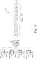
- Figure 2 depicts a pictorial representation of an example frame structure 200 , which illustrates key principles of the present invention.
- the frame structure 200 shown in Figure 2 illustrates how the present invention allocates bandwidth proportionally, which allows a user to maximize the amount of bandwidth that can be transported on the serial bit stream.
- the present invention enables users to transport different bandwidths efficiently on a plurality of wideband channels, instead of having to transport equal amounts of bandwidth inefficiently on those channels.
- bandwidth A (5 MHz RF) is input to A/D DDC device 202a
- bandwidth B (40 MHz RF) is input to A/D DDC device 202b
- bandwidth C (25 MHz RF) is input to A/D DDC device 202c
- bandwidth D (5 MHz RF) is input to A/D DDC device 202d
- a respective sample clock 204a-204d inputs a unique sample rate to the associated A/D DDC device 202a-202d .
- A/D devices 202a-202d are coupled to a mapper/framer device 206 and a serializer device (not shown), which multiplexes or combines the separate bandwidth segments (A, B, C, D) and constructs a suitable frame 208 including the bandwidth segments for transport.
- a mapper/framer device 206 and a serializer device (not shown), which multiplexes or combines the separate bandwidth segments (A, B, C, D) and constructs a suitable frame 208 including the bandwidth segments for transport.
- a serializer device not shown
- the sample rate of sample clock 204a is selected to be approximately 15 Msps (for 5 MHz bandwidth segments), approximately 90 Msps for sample clock 204b (for 40 MHz bandwidth segments), approximately 60 Msps for sample clock 204c (for 25 MHz bandwidth segments), and approximately 15 Msps for sample clock 204d (for 5 MHz bandwidth segments).
- the bandwidths in frame 208 are allocated proportionally, by transporting one slot for bandwidth A (5 MHz), six slots for bandwidth B (40 MHz), four slots for bandwidth C (25 MHz), and one slot for bandwidth D (5 MHz).
Landscapes
- Engineering & Computer Science (AREA)
- Computer Networks & Wireless Communication (AREA)
- Signal Processing (AREA)
- Optical Communication System (AREA)
- Time-Division Multiplex Systems (AREA)
Description
- The present invention relates generally to the telecommunications field, and more specifically, but not exclusively, to a system and method for enhancing the performance of wideband digital Radio Frequency (RF) transport systems.
- In wireless voice and data communications, the digital transport of RF signals over long distances via fiber optic cables provides enhanced capacity, and higher performance distributed coverage than existing analog RF transport systems currently being used. An example of such a digital RF transport system that links a digital host unit to one or more digital remote units to perform bi-directional simultaneous digital RF distribution is disclosed in
U.S. Patent Application Publication No. 2004/0132474 A1 , entitled "POINT-TO-MULTIPOINT DIGITAL RADIO FREQUENCY TRANSPORT", which is assigned to ADC Telecommunications, Inc. of Eden Prairie, MN. - Notwithstanding the advantages of today's digital RF transport systems over other types of RF transport systems, a significant problem exists in the transport of large amounts of digital RF bandwidth (e.g., wideband). For example, the existing wideband digital RF transport systems combine multiple digitized signals and convey them in serialized form on a common physical layer between the transmit and receive devices involved. However, the problem with the existing digital RF transport systems is that they inefficiently transport equal amounts of bandwidth for different wideband channels. In other words, the serial bit streams on the transport layer that convey N wideband channels are all tied to one sample rate, and the system transport spectrum (RF) is sent point-to-point in equal bandwidth segments (e.g., 25 MHz blocks). Consequently, since many of the wideband channels have bandwidth requirements that are less (or different) than 25 MHz (e.g., 5 MHz, 10 MHz, 30 MHz, etc.), the overall bandwidths of existing wideband digital RF transport systems are substantially underutilized. Therefore, a pressing need exists for a system and method that can enhance the performance of wideband digital RF transport systems, by maximizing the utilization of the transport bandwidth, custom tailoring the bandwidth allocations to specific user needs on a common platform, and enabling the use of lower cost transport system devices. As described in detail below, the present invention provides such a system and method, which resolves the above-described bandwidth underutilization problems and other related problems.
-
US 5,818,883 discloses a multi-channel digital transceiver which receives uplink RF signals and converts them into digital IF signals. A digital down converter selects a particular frequency, decimates and filters the selected signal to a bandwidth associated with the channels of the system. - The present invention provides a system and method for enhancing the performance of wideband digital RF transport systems, which enables the transport of different bandwidth segments on a plurality of wideband channels by selecting an optimal clock sample rate for each bandwidth segment to be transported. Thus, the present invention allocates the bandwidth segments proportionally so that an optimum amount of bandwidth can be transported at the serial bit rate.
- Aspects of the invention are defined by the claims appended hereto.
- In accordance with a preferred example of the present invention, a system for enhancing the performance of a wideband digital RF transport system is provided, which includes a transmit unit, a receive unit, and an optical transmission medium connected between the transmit unit and the receive unit. The transmit unit includes a plurality of wideband RF analog signal inputs coupled to a plurality of analog-to-digital, digital down-converter (A/D DDC) devices. Notably, the sample rate of each A/D DDC device is determined by a respective sample clock. The digitized wideband RF signal segments at the outputs of the A/D DDC devices are combined and converted to a frame structure, converted to serial form, and transmitted on the optical transmission medium to the receive unit. A light detection device in the receive unit detects the serial bit stream of frames on the optical transmission medium, the serialized frames are converted back to the original frame format, and the original digitized wideband RF segments are reconstructed. Each digitized wideband RF segment is coupled to a respective D/A digital up-converter (D/A DUC) device associated with a particular wideband RF signal input on the transmit side. Notably, the output sample rate of each D/A DUC device is determined by a respective sample clock, which provides the same sample rate as that of the associated A/D DDC device in the transmit unit. The sample rate of each A/D DDC device (and associated D/A DUC device) is pre- selected so that the transmission medium can transport the optimum amount of RF bandwidth at the given serial bit rate.
- The novel features believed characteristic of the invention are set forth in the appended claims. The invention itself, however, as well as a preferred mode of use, further objectives and advantages thereof, will best be understood by reference to the following detailed description of an illustrative embodiment when read in conjunction with the accompanying drawing(s), wherein:
-
Figure 1 depicts a schematic block diagram of an example system for enhancing the performance of wideband digital RF transport systems, which can be used to implement a preferred embodiment of the present invention; and -
Figure 2 depicts a pictorial representation of an example frame structure, which illustrates key principles of the present invention. - With reference now to the figures,
Figure 1 depicts a schematic block diagram of anexample system 100 for enhancing the performance of wideband digital RF transport systems, which can be used to implement a preferred embodiment of the present invention.System 100 includes afirst communications unit 101, asecond communications unit 103, and a transmission (transport)medium 111 connected betweenfirst communications unit 101 andsecond communications unit 103. For this example embodiment,first communications unit 101 is a wideband digital RF transmit unit,second communications unit 103 is a wideband digital RF receive unit, andtransmission medium 111 is a single mode (or multi-mode) fiber optic cable. Althoughsystem 100 is depicted for illustrative purposes as a unidirectional communications system, the scope of coverage of the present invention is not intended to be so limited, andsystem 100 could also be implemented as a bi-directional communications system (e.g., using a transceiver on each side). Also, for this illustrative example,system 100 may be implemented as a point-to-point digital RF transport system for cellular radiotelephone voice and data communications, with a digital host unit (first communications unit 101) that provides an interface between a plurality of base station RF ports and the fiber optic cable, and a digital remote unit (second communications unit 103) that provides an interface between the fiber optic cable and a remote antenna. Additionally, although thetransmission medium 111 is described as an optical transmission medium for this illustrative embodiment, the present invention is not intended to be so limited and can include within its scope any suitable transmission medium (e.g., millimeter wave radio link, microwave radio link, satellite radio link, infrared wireless link, coaxial cable, etc.) capable of transporting a serial bit stream. - For this example embodiment,
first communications unit 101 includes a plurality ofinput interfaces 102a-102n. Eachinput interface 102a-102n is implemented with an A/D DDC device, for this illustrative embodiment. An input of each A/D DDC device 102a-102n couples a respective analog frequency band (or channel) into the associated A/D DDC device. For example, each A/D DDC device 102a-102n can accept an input analog frequency band (e.g., frequency band from a base transceiver station) at a relatively high rate, and digitizes and down-converts the respective frequency band to suitable digital real and complex (e.g., I/Q) baseband signals. For example, the output from each A/D converter section of an A/D DDC device 102a-102n can be a sequence of real samples, representing a real (positive frequency) signal within a designated Nyquist zone. The output from each DDC section can be a baseband signal (centered at zero Hz) with positive and negative frequencies, composed of two sample streams (real and imaginary components) with each stream at one half the sample rate of the equivalent real-valued signal. - Notably, in the example embodiment depicted in
Figure 1 , theinput interfaces 102a-102n tocommunications unit 101 are implemented with a plurality of A/D DDC devices that can accept a plurality of analog RF bandwidths, but the present invention is not intended to be so limited. In other embodiments, the input interfaces can be implemented with other types of input devices to accept other types of bandwidths. For example, in order to accept a plurality of RF inputs, eachinput interface device 102a-102n can be implemented with a single A/D converter (no DDC) operating at IF (e.g., real digital output), dual A/D converters (no DDC) operating at baseband (e.g., complex I/Q digital output), or single or dual A/D converters operating at a high sample rate and followed by digital down-conversion (DDC) whereby the output is a lower sample rate representation (complex I/Q) of a portion of the original band. In another embodiment, eachinput interface device 102a-102n can be implemented by a direct digital input (typically baseband I/Q) from a digital or "software-defined" base station. In sum, the plurality ofinput interfaces 102a-102n can be implemented with any suitable input interface device(s) capable of accepting or inputting analog or digital wideband segments. - For this example embodiment, each A/
D DDC device 102a-102n can be implemented as part of a modular (e.g., pluggable) RF card capable of adjustable bandwidth selection that can be determined by user requirements. For example, in one embodiment, each A/D DDC device 102a-102n can be implemented as part of an RF card that passes 5 MHz bandwidth segments. Notably, the sample rate of each A/D DDC device 102a-102n is determined by an associatedsample clock 104a-104n. Therefore, by selecting a suitable sample rate for each A/D DDC device 102a-102n, the present invention provides the ability to custom tailor the bandwidth allocations to specific user needs on the common transport platform being used. - For example, one or more users may desire to transport a combination of one 5 MHz segment and three 15 MHz segments from a digital host unit (e.g., first communications unit 101) to a digital remote unit (e.g., second communications unit 103) via a fiber optic cable (e.g., transmission medium 111). For a given serial bit rate on the fiber optic cable, a suitable sample rate may be selected for the
sample clock 104a-104n associated with each A/D DDC device 102a-102n to be used. For this example, assume that the 5 MHz segment is to be input to A/D DDC device 102a, and each of A/D DDC devices 102b, 102c and 102d (where "n" in this case is equal to 4) is designed to accept a respective one of the three 15 MHz segments to be transported. The sample rate forsample clock 104a is selected to accommodate the transport of the 5 MHz segment (band) at the given serial bit rate, and the sample rates forsample clocks 104b-104d are selected to accommodate the transport of the respective 15 MHz segments at the given serial bit rate. In a practical application, the sample rates (e.g., approximately 45 Msps) ofsample clocks 104b-104d are typically three times the sample rate ofsample clock 104a (e.g., approximately 15 Msps) for a given serial bit rate on a fiber optic cable. In any event it should be readily understood that the present invention is not intended to be limited to a particular set of clock sample rates, the size of a frequency band that can be accepted by a specific A/D DDC device, the size of the frequency bands to be transported, or the serial bit rate for the optical transmission medium to be used. - For example, a suitable clock sample rate can be selected to accommodate the transport of a 75 MHz segment (e.g., at 15 times the clock sample rate used for a 5 MHz segment) from the input of a particular A/D DDC device via a fiber optic cable at a specific serial bit rate. As another example, assume that each A/
D DDC device 102a-102n is designed to process a 10 MHz band of frequencies. In this case, a suitable sample rate for each sample clock can be selected to accommodate the transport of a 10 MHz band and/or a band that is a multiple of 10 MHz (e.g., 30 MHz band at three times the sample rate of the sample rate used for the 10 MHz band). In other words, the present invention enables a user to transport just the required amount of bandwidth at the serial bit rate of the transmission medium to be used. - For this example embodiment, the digitized output of each A/
D DDC device 102a-102n is coupled to a mapper/framer device 106. Essentially, the mapper section of mapper/framer device 106 multiplexes together the digitized bands at the outputs of the plurality of A/D DDC devices 102a-102n, and the framer section of mapper/framer device 106 converts the multiplexed digitized bands into a suitable frame structure format. For example, in a practical application, the mapper/framer device 106 can construct a suitable frame structure that provides up to twelve (e.g., 5 MHz) slots per frame. However, it should be understood that the present invention is not intended to be limited to a specific number of slots per frame, and any suitable number of slots per frame may be used. In any event, the frame(s) containing the multiplexed band segments are coupled from mapper/framer device 106 to aserializer device 108, which converts the parallel frame data from the mapper/framer device 106 to a serial bit stream. The serial data fromserializer device 108 is coupled to an optical transmitdevice 110. The optical transmitdevice 110 processes and translates that data into coded light pulses that form a serial bit stream. An injection-laser diode or other suitable light source generates the light pulses, which are funneled with suitable optical lenses into the optical transmission medium (e.g., fiber optic cable) 111. For example,optical transmission medium 111 can be a single mode or multi-mode fiber optic cable. Notably, an optical transport medium is used for this illustrative embodiment, but the present invention is not intended to be so limited and can include within its scope of coverage any suitable transport medium that can convey a serial bit stream. - For this example embodiment,
second communications unit 103 includes a receivedevice 112, which includes a light sensitive device that detects the pulsed light signals (e.g., serial bit stream of frames) ontransmission medium 111, converts the light signals to digital signals, and conveys them in serial form to adeserializer device 114. Again, it should be understood that although a light sensitive device is used for this illustrative embodiment, the present invention is not intended to be so limited and can include within its scope of coverage any suitable device that can receive and/or detect a serial bit stream from the particular transport medium being used.Deserializer device 114 converts the serial frame data from receivedevice 112 to parallel frame data, which is coupled to a demapper/deframer device 116. Essentially, demapper/deframer device 116 demultiplexes the parallel frame data, and extracts the bandwidth segments from the demultiplexed frames. The extracted bandwidth segments are coupled to the inputs of theappropriate output interfaces 118a-118n. For this illustrative embodiment, eachoutput interface 118a-118n is implemented with a digital-to-analog (D/A) digital up-converter (D/A DUC) device. Each D/A DUC device 118a-118n converts the complex digital baseband signal to a real passband signal. For example, each digital baseband signal can be filtered, converted to the appropriate sampling rate by a respective sample clock 120a-120n, upconverted to an appropriate frequency, and modulated onto an analog signal. For this example embodiment, the sample rate of each sample clock 120a-120n is selected to be the same as the sample rate of thecorresponding sample clock 104a-104n infirst communications unit 101. Thus, the analog bandwidth segments input tofirst communications unit 101 are transported viaoptical transmission medium 111 as a serial bit stream, and reconstructed at the corresponding output insecond communications unit 103. - Notably, in the example embodiment depicted in
Figure 1 , theoutput interfaces 102a-102n ofcommunications unit 103 are implemented with a plurality of D/A DUC devices that can output a plurality of analog RF bandwidths, but the present invention is not intended to be so limited. In other embodiments, the output interfaces can be implemented with other types of output devices for other types of bandwidths. For example, in a second embodiment, in order to process a real digital signal at its input, eachoutput interface 118a-118n can be implemented with a single D/A converter and analog up-conversion. In another embodiment, in order to process a complex digital signal at its input, eachoutput interface 118a-118n can be implemented with dual D/A converters and analog up-conversion, or a DUC (e.g., digital up-conversion) and dual D/A converters. In sum, the plurality ofoutput interfaces 118a-118n can be implemented with any suitable output interface device(s) capable of outputting analog or digital wideband segments. -
Figure 2 depicts a pictorial representation of anexample frame structure 200, which illustrates key principles of the present invention. Essentially, theframe structure 200 shown inFigure 2 illustrates how the present invention allocates bandwidth proportionally, which allows a user to maximize the amount of bandwidth that can be transported on the serial bit stream. As such, the present invention enables users to transport different bandwidths efficiently on a plurality of wideband channels, instead of having to transport equal amounts of bandwidth inefficiently on those channels. - Specifically, referring to this illustrative example, it may be assumed that four different bandwidths are to be transported by
system 100 depicted inFigure 1 . As such, for this example, bandwidth A (5 MHz RF) is input to A/D DDC device 202a, bandwidth B (40 MHz RF) is input to A/D DDC device 202b, bandwidth C (25 MHz RF) is input to A/D DDC device 202c, and bandwidth D (5 MHz RF) is input to A/D DDC device 202d. Arespective sample clock 204a-204d inputs a unique sample rate to the associated A/D DDC device 202a-202d. The outputs from A/D devices 202a-202d are coupled to a mapper/framer device 206 and a serializer device (not shown), which multiplexes or combines the separate bandwidth segments (A, B, C, D) and constructs asuitable frame 208 including the bandwidth segments for transport. For this example frame structure, assume that the frame rate is approximately 15 MHz, and each of the frame's 12 slots includes 16 bits of digitized RF (with 14 bits of payload). The sample rate ofsample clock 204a is selected to be approximately 15 Msps (for 5 MHz bandwidth segments), approximately 90 Msps forsample clock 204b (for 40 MHz bandwidth segments), approximately 60 Msps forsample clock 204c (for 25 MHz bandwidth segments), and approximately 15 Msps forsample clock 204d (for 5 MHz bandwidth segments). Thus, as illustrated by this example, the bandwidths inframe 208 are allocated proportionally, by transporting one slot for bandwidth A (5 MHz), six slots for bandwidth B (40 MHz), four slots for bandwidth C (25 MHz), and one slot for bandwidth D (5 MHz). - The description of the present invention has been presented for purposes of illustration and description, and is not intended to be exhaustive or limited to the invention in the form disclosed. Many modifications and variations will be apparent to those of ordinary skill in the art. These embodiments were chosen and described in order to best explain the principles of the invention, the practical application, and to enable others of ordinary skill in the art to understand the invention for various embodiments with various modifications as are suited to the particular use contemplated.
Claims (14)
- A host unit (101) of a wideband digital RF transport system (100), comprising:a plurality of input devices (102a-102n), each input device configured to receive an analog frequency band; anda plurality of sample rate devices (104a-104n) coupled to said plurality of input devices (102a-102n), characterized in that each sample rate device of said plurality of sample rate devices is adapted to set a unique sample rate of an associated input device based on the bandwidth of the received analog frequency band for that input device so that the analog frequency band associated with each input device is sampled for transport, in a frame (208) with the other sampled analog frequency bands, to a remote unit (103).
- The host unit (101) of Claim 1, further comprising:a mapper/framer device (106), an output of each input device coupled to an input of said mapper/framer device;a serializer device (108) coupled to an output of said mapper/framer device;a transmit device (110) coupled to an output of said serializer device; anda transmission medium (111) coupled to an output of said transmit device.
- The host unit of Claim 2, wherein said transmit device (110) comprises at least one of: a millimeter wave radio transmitter device; a wireless transmitter device; and a laser transmitter device.
- The host unit of Claim 2, wherein said transmit device (110) comprises a laser transmitter device, and said transmission medium comprises a fiber optic cable.
- The host unit of Claim 1, wherein said plurality of input devices comprises a plurality of analog-to-digital digital down-converters (102a-102n).
- The host unit of Claim 1, wherein said plurality of sample rate devices comprises a plurality of sample clocks (104a-104n).
- A system for wideband digital RF transport (100), comprising the host unit (101) of any one of claims 1 to 6 and a remote unit (103), said remote unit (103) comprising:means (112) for detecting at least one frame from a received signal, coupled to a transmission medium (111);means (114) for converting said detected at least one frame to a parallel form;means (116) for deconstructing said at least one frame to produce a combined plurality of sampled frequency bands;means for separating said combined plurality of sampled frequency bands;means (118a-118n) for converting said plurality of sampled frequency bands to a second plurality of analog frequency bands; andmeans (120a-120n) for setting an output sample rate for each analog frequency band of said second plurality of analog frequency bands.
- The system of Claim 7, wherein said means for converting said plurality of sampled frequency bands to a second plurality of analog frequency bands comprises a plurality of digital-to-analog digital up-converter devices (118a-118n), and said means for setting an output sample rate for each analog frequency band of said second plurality of analog frequency bands comprises a second plurality of sample clocks (120a-120n).
- A method for wideband digital RF transport, comprising the steps of :inputting a plurality of analog frequency bands; the method characterized by setting a unique input sample rate for each analog frequency band of said plurality of analog frequency bands based on the bandwidth of the received analog frequency band so that each of the analog frequency bands is sampled for transport to a remote unit;combining said plurality of sampled frequency bands; andconverting said combined plurality of sampled frequency bands to at least one frame structure.
- The method of Claim 9, further comprising the steps of:converting said at least one frame structure to a serial data stream; andtransmitting said serial data stream on a transmission medium (111).
- The method of Claim 9, wherein the inputting step is performed by a plurality of input devices (102a-102n), and the setting step is performed by a first plurality of sample clock devices (104a-104n).
- The method of Claim 9, further comprising the steps of:detecting said at least one frame (208) from said serial data stream;converting said detected at least one frame to a parallel form;deconstructing said at least one frame to produce said combined plurality of sampled frequency bands;separating said combined plurality of sampled frequency bands;converting said plurality of sampled frequency bands to a second plurality of analog frequency bands; andsetting an output sample rate for each analog frequency band of said second plurality of analog frequency bands.
- The method of Claim 12, wherein the step of converting said plurality of sampled frequency bands to a second plurality of analog frequency bands is performed by a plurality of output devices.
- The method of Claim 12, wherein the step of setting an output sample rate is performed by a second plurality of sample clock devices (120a-120n).
Priority Applications (3)
| Application Number | Priority Date | Filing Date | Title |
|---|---|---|---|
| EP18205036.9A EP3468076B1 (en) | 2006-04-06 | 2007-04-06 | System and method for enhancing the performance of wideband digital rf transport systems |
| EP20177347.0A EP3751760A1 (en) | 2006-04-06 | 2007-04-06 | System and method for enhancing the performance of wideband digital rf transport systems |
| EP17020235.2A EP3267602B1 (en) | 2006-04-06 | 2007-04-06 | System and method for enhancing the performance of wideband digital rf transport systems |
Applications Claiming Priority (2)
| Application Number | Priority Date | Filing Date | Title |
|---|---|---|---|
| US11/398,879 US7610046B2 (en) | 2006-04-06 | 2006-04-06 | System and method for enhancing the performance of wideband digital RF transport systems |
| PCT/US2007/066144 WO2007118195A1 (en) | 2006-04-06 | 2007-04-06 | System and method for enhancing the performance of wideband digital rf transport systems |
Related Child Applications (3)
| Application Number | Title | Priority Date | Filing Date |
|---|---|---|---|
| EP17020235.2A Division EP3267602B1 (en) | 2006-04-06 | 2007-04-06 | System and method for enhancing the performance of wideband digital rf transport systems |
| EP20177347.0A Division EP3751760A1 (en) | 2006-04-06 | 2007-04-06 | System and method for enhancing the performance of wideband digital rf transport systems |
| EP18205036.9A Division EP3468076B1 (en) | 2006-04-06 | 2007-04-06 | System and method for enhancing the performance of wideband digital rf transport systems |
Publications (2)
| Publication Number | Publication Date |
|---|---|
| EP2005627A1 EP2005627A1 (en) | 2008-12-24 |
| EP2005627B1 true EP2005627B1 (en) | 2017-06-07 |
Family
ID=38370415
Family Applications (4)
| Application Number | Title | Priority Date | Filing Date |
|---|---|---|---|
| EP18205036.9A Active EP3468076B1 (en) | 2006-04-06 | 2007-04-06 | System and method for enhancing the performance of wideband digital rf transport systems |
| EP20177347.0A Pending EP3751760A1 (en) | 2006-04-06 | 2007-04-06 | System and method for enhancing the performance of wideband digital rf transport systems |
| EP17020235.2A Active EP3267602B1 (en) | 2006-04-06 | 2007-04-06 | System and method for enhancing the performance of wideband digital rf transport systems |
| EP07760252.2A Active EP2005627B1 (en) | 2006-04-06 | 2007-04-06 | System and method for enhancing the performance of wideband digital rf transport systems |
Family Applications Before (3)
| Application Number | Title | Priority Date | Filing Date |
|---|---|---|---|
| EP18205036.9A Active EP3468076B1 (en) | 2006-04-06 | 2007-04-06 | System and method for enhancing the performance of wideband digital rf transport systems |
| EP20177347.0A Pending EP3751760A1 (en) | 2006-04-06 | 2007-04-06 | System and method for enhancing the performance of wideband digital rf transport systems |
| EP17020235.2A Active EP3267602B1 (en) | 2006-04-06 | 2007-04-06 | System and method for enhancing the performance of wideband digital rf transport systems |
Country Status (4)
| Country | Link |
|---|---|
| US (2) | US7610046B2 (en) |
| EP (4) | EP3468076B1 (en) |
| CN (2) | CN102868475B (en) |
| WO (1) | WO2007118195A1 (en) |
Families Citing this family (91)
| Publication number | Priority date | Publication date | Assignee | Title |
|---|---|---|---|---|
| DE60139116D1 (en) | 2000-03-27 | 2009-08-13 | Opencell Corp | System for distributing multiprotocol RF signals |
| US6704545B1 (en) | 2000-07-19 | 2004-03-09 | Adc Telecommunications, Inc. | Point-to-multipoint digital radio frequency transport |
| US8811917B2 (en) | 2002-05-01 | 2014-08-19 | Dali Systems Co. Ltd. | Digital hybrid mode power amplifier system |
| US8380143B2 (en) | 2002-05-01 | 2013-02-19 | Dali Systems Co. Ltd | Power amplifier time-delay invariant predistortion methods and apparatus |
| US8958789B2 (en) | 2002-12-03 | 2015-02-17 | Adc Telecommunications, Inc. | Distributed digital antenna system |
| US7610046B2 (en) * | 2006-04-06 | 2009-10-27 | Adc Telecommunications, Inc. | System and method for enhancing the performance of wideband digital RF transport systems |
| US8873585B2 (en) | 2006-12-19 | 2014-10-28 | Corning Optical Communications Wireless Ltd | Distributed antenna system for MIMO technologies |
| KR20100014339A (en) | 2006-12-26 | 2010-02-10 | 달리 시스템즈 씨오. 엘티디. | Method and system for baseband predistortion linearization in multi-channel wideband communication systems |
| US20080240225A1 (en) * | 2007-03-27 | 2008-10-02 | Adc Telecommunications, Inc. | Method and system for enhancing the performance of wideband digital rf transport systems |
| US20100054746A1 (en) | 2007-07-24 | 2010-03-04 | Eric Raymond Logan | Multi-port accumulator for radio-over-fiber (RoF) wireless picocellular systems |
| US8175459B2 (en) | 2007-10-12 | 2012-05-08 | Corning Cable Systems Llc | Hybrid wireless/wired RoF transponder and hybrid RoF communication system using same |
| WO2009081376A2 (en) | 2007-12-20 | 2009-07-02 | Mobileaccess Networks Ltd. | Extending outdoor location based services and applications into enclosed areas |
| JP5359179B2 (en) * | 2008-10-17 | 2013-12-04 | 富士通株式会社 | Optical receiver and optical receiving method |
| KR101503324B1 (en) * | 2009-01-13 | 2015-03-24 | 에이디씨 텔레커뮤니케이션스 인코포레이티드 | Systems and methods for improved digital rf transport in distributed antenna systems |
| US9673904B2 (en) | 2009-02-03 | 2017-06-06 | Corning Optical Communications LLC | Optical fiber-based distributed antenna systems, components, and related methods for calibration thereof |
| AU2010210766A1 (en) | 2009-02-03 | 2011-09-15 | Corning Cable Systems Llc | Optical fiber-based distributed antenna systems, components, and related methods for monitoring and configuring thereof |
| WO2010091004A1 (en) | 2009-02-03 | 2010-08-12 | Corning Cable Systems Llc | Optical fiber-based distributed antenna systems, components, and related methods for calibration thereof |
| US20100208777A1 (en) * | 2009-02-17 | 2010-08-19 | Adc Telecommunications, Inc. | Distributed antenna system using gigabit ethernet physical layer device |
| US8346091B2 (en) * | 2009-04-29 | 2013-01-01 | Andrew Llc | Distributed antenna system for wireless network systems |
| US9590733B2 (en) | 2009-07-24 | 2017-03-07 | Corning Optical Communications LLC | Location tracking using fiber optic array cables and related systems and methods |
| US7903010B1 (en) * | 2009-08-31 | 2011-03-08 | Cirrus Logic, Inc. | Delta-sigma analog-to-digital converter (ADC) having a serialized quantizer output |
| US8280259B2 (en) | 2009-11-13 | 2012-10-02 | Corning Cable Systems Llc | Radio-over-fiber (RoF) system for protocol-independent wired and/or wireless communication |
| CN101718944B (en) * | 2009-12-29 | 2011-06-08 | 上海交通大学 | Multi-wavelength space-division optical analog-digital converter |
| US8275265B2 (en) | 2010-02-15 | 2012-09-25 | Corning Cable Systems Llc | Dynamic cell bonding (DCB) for radio-over-fiber (RoF)-based networks and communication systems and related methods |
| CN102845001B (en) | 2010-03-31 | 2016-07-06 | 康宁光缆系统有限责任公司 | Based on positioning service in the distributed communication assembly of optical fiber and system and associated method |
| DE102010018492B4 (en) | 2010-04-28 | 2011-12-08 | Andrew Wireless Systems Gmbh | Interface module for a unit of an antenna distribution system and antenna distribution system |
| US8570914B2 (en) | 2010-08-09 | 2013-10-29 | Corning Cable Systems Llc | Apparatuses, systems, and methods for determining location of a mobile device(s) in a distributed antenna system(s) |
| US8848766B2 (en) | 2010-08-17 | 2014-09-30 | Dali Systems Co. Ltd. | Neutral host architecture for a distributed antenna system |
| KR102136940B1 (en) | 2010-09-14 | 2020-07-23 | 달리 시스템즈 씨오. 엘티디. | Remotely Reconfigurable Distributed Antenna System and Methods |
| US9160449B2 (en) | 2010-10-13 | 2015-10-13 | Ccs Technology, Inc. | Local power management for remote antenna units in distributed antenna systems |
| US9252874B2 (en) | 2010-10-13 | 2016-02-02 | Ccs Technology, Inc | Power management for remote antenna units in distributed antenna systems |
| EP2630759B1 (en) | 2010-10-19 | 2019-03-20 | CommScope Technologies LLC | Systems and methods for transporting digital rf signals |
| US11296504B2 (en) | 2010-11-24 | 2022-04-05 | Corning Optical Communications LLC | Power distribution module(s) capable of hot connection and/or disconnection for wireless communication systems, and related power units, components, and methods |
| EP2643947B1 (en) | 2010-11-24 | 2018-09-19 | Corning Optical Communications LLC | Power distribution module(s) capable of hot connection and/or disconnection for distributed antenna systems, and related power units, components, and methods |
| CN103201958B (en) | 2011-02-07 | 2017-01-18 | 大力系统有限公司 | Daisy-chained ring of remote units for distributed antenna systems |
| US8659453B1 (en) * | 2011-04-07 | 2014-02-25 | Lockheed Martin Corporation | Digital radio frequency memory utilizing time interleaved analog to digital converters and time interleaved digital to analog converters |
| WO2012148938A1 (en) | 2011-04-29 | 2012-11-01 | Corning Cable Systems Llc | Determining propagation delay of communications in distributed antenna systems, and related components, systems and methods |
| CN103609146B (en) | 2011-04-29 | 2017-05-31 | 康宁光缆系统有限责任公司 | Systems, methods and apparatus for increasing radio frequency (RF) power in a distributed antenna system |
| WO2013033199A1 (en) | 2011-08-29 | 2013-03-07 | Andrew Llc | Configuring a distributed antenna system |
| CN102448052B (en) * | 2011-12-06 | 2015-02-04 | 京信通信系统(中国)有限公司 | Multi-service mixed signal transmission method, device and system |
| EP2832012A1 (en) | 2012-03-30 | 2015-02-04 | Corning Optical Communications LLC | Reducing location-dependent interference in distributed antenna systems operating in multiple-input, multiple-output (mimo) configuration, and related components, systems, and methods |
| US9781553B2 (en) | 2012-04-24 | 2017-10-03 | Corning Optical Communications LLC | Location based services in a distributed communication system, and related components and methods |
| WO2013162988A1 (en) | 2012-04-25 | 2013-10-31 | Corning Cable Systems Llc | Distributed antenna system architectures |
| US8917996B2 (en) * | 2012-06-13 | 2014-12-23 | Raytheon Company | Simplified serial data over optical fiber for remote receiver/sensor applications |
| US9154222B2 (en) | 2012-07-31 | 2015-10-06 | Corning Optical Communications LLC | Cooling system control in distributed antenna systems |
| EP2883416A1 (en) | 2012-08-07 | 2015-06-17 | Corning Optical Communications Wireless Ltd. | Distribution of time-division multiplexed (tdm) management services in a distributed antenna system, and related components, systems, and methods |
| CN104782093B (en) | 2012-10-31 | 2018-02-27 | 康普技术有限责任公司 | Digital Baseband Transmission in Telecommunication Distribution System |
| US9455784B2 (en) | 2012-10-31 | 2016-09-27 | Corning Optical Communications Wireless Ltd | Deployable wireless infrastructures and methods of deploying wireless infrastructures |
| CA2892508A1 (en) | 2012-11-26 | 2014-05-30 | Adc Telecommunications, Inc. | Timeslot mapping and/or aggregation element for digital radio frequency transport architecture |
| US10257056B2 (en) | 2012-11-28 | 2019-04-09 | Corning Optical Communications LLC | Power management for distributed communication systems, and related components, systems, and methods |
| EP2926466A1 (en) | 2012-11-29 | 2015-10-07 | Corning Optical Communications LLC | HYBRID INTRA-CELL / INTER-CELL REMOTE UNIT ANTENNA BONDING IN MULTIPLE-INPUT, MULTIPLE-OUTPUT (MIMO) DISTRIBUTED ANTENNA SYSTEMS (DASs) |
| US9647758B2 (en) | 2012-11-30 | 2017-05-09 | Corning Optical Communications Wireless Ltd | Cabling connectivity monitoring and verification |
| US9158864B2 (en) | 2012-12-21 | 2015-10-13 | Corning Optical Communications Wireless Ltd | Systems, methods, and devices for documenting a location of installed equipment |
| US9497706B2 (en) | 2013-02-20 | 2016-11-15 | Corning Optical Communications Wireless Ltd | Power management in distributed antenna systems (DASs), and related components, systems, and methods |
| WO2014199380A1 (en) | 2013-06-12 | 2014-12-18 | Corning Optical Communications Wireless, Ltd. | Time-division duplexing (tdd) in distributed communications systems, including distributed antenna systems (dass) |
| CN105452951B (en) | 2013-06-12 | 2018-10-19 | 康宁光电通信无线公司 | Voltage type optical directional coupler |
| US11425579B2 (en) | 2013-07-09 | 2022-08-23 | Commscope Technologies Llc | Signal distribution interface |
| US9247543B2 (en) | 2013-07-23 | 2016-01-26 | Corning Optical Communications Wireless Ltd | Monitoring non-supported wireless spectrum within coverage areas of distributed antenna systems (DASs) |
| US9661781B2 (en) | 2013-07-31 | 2017-05-23 | Corning Optical Communications Wireless Ltd | Remote units for distributed communication systems and related installation methods and apparatuses |
| WO2015029028A1 (en) | 2013-08-28 | 2015-03-05 | Corning Optical Communications Wireless Ltd. | Power management for distributed communication systems, and related components, systems, and methods |
| US9209842B2 (en) * | 2013-09-09 | 2015-12-08 | Texas Instruments Incorporated | Method and circuitry for transmitting data |
| US9385810B2 (en) | 2013-09-30 | 2016-07-05 | Corning Optical Communications Wireless Ltd | Connection mapping in distributed communication systems |
| CN103560851A (en) * | 2013-10-28 | 2014-02-05 | 深圳市冠标科技发展有限公司 | Method for wireless audio single-frequency multichannel transmission |
| WO2015079435A1 (en) | 2013-11-26 | 2015-06-04 | Corning Optical Communications Wireless Ltd. | Selective activation of communications services on power-up of a remote unit(s) in a distributed antenna system (das) based on power consumption |
| US20170250927A1 (en) * | 2013-12-23 | 2017-08-31 | Dali Systems Co. Ltd. | Virtual radio access network using software-defined network of remotes and digital multiplexing switches |
| CN103675848A (en) * | 2013-12-26 | 2014-03-26 | 东莞市泰斗微电子科技有限公司 | Signal transmission method and system based on multichannel GNSS signals |
| US9178635B2 (en) | 2014-01-03 | 2015-11-03 | Corning Optical Communications Wireless Ltd | Separation of communication signal sub-bands in distributed antenna systems (DASs) to reduce interference |
| EP3108627A4 (en) | 2014-02-18 | 2017-10-11 | CommScope Technologies LLC | Selectively combining uplink signals in distributed antenna systems |
| US9775123B2 (en) | 2014-03-28 | 2017-09-26 | Corning Optical Communications Wireless Ltd. | Individualized gain control of uplink paths in remote units in a distributed antenna system (DAS) based on individual remote unit contribution to combined uplink power |
| US9357551B2 (en) | 2014-05-30 | 2016-05-31 | Corning Optical Communications Wireless Ltd | Systems and methods for simultaneous sampling of serial digital data streams from multiple analog-to-digital converters (ADCS), including in distributed antenna systems |
| CN105322916A (en) * | 2014-06-10 | 2016-02-10 | 深圳市中兴微电子技术有限公司 | Filtering method and filter |
| US9509133B2 (en) | 2014-06-27 | 2016-11-29 | Corning Optical Communications Wireless Ltd | Protection of distributed antenna systems |
| US9525472B2 (en) | 2014-07-30 | 2016-12-20 | Corning Incorporated | Reducing location-dependent destructive interference in distributed antenna systems (DASS) operating in multiple-input, multiple-output (MIMO) configuration, and related components, systems, and methods |
| US9730228B2 (en) | 2014-08-29 | 2017-08-08 | Corning Optical Communications Wireless Ltd | Individualized gain control of remote uplink band paths in a remote unit in a distributed antenna system (DAS), based on combined uplink power level in the remote unit |
| US9653861B2 (en) | 2014-09-17 | 2017-05-16 | Corning Optical Communications Wireless Ltd | Interconnection of hardware components |
| US9602210B2 (en) | 2014-09-24 | 2017-03-21 | Corning Optical Communications Wireless Ltd | Flexible head-end chassis supporting automatic identification and interconnection of radio interface modules and optical interface modules in an optical fiber-based distributed antenna system (DAS) |
| US9420542B2 (en) | 2014-09-25 | 2016-08-16 | Corning Optical Communications Wireless Ltd | System-wide uplink band gain control in a distributed antenna system (DAS), based on per band gain control of remote uplink paths in remote units |
| US9729267B2 (en) | 2014-12-11 | 2017-08-08 | Corning Optical Communications Wireless Ltd | Multiplexing two separate optical links with the same wavelength using asymmetric combining and splitting |
| US20160249365A1 (en) | 2015-02-19 | 2016-08-25 | Corning Optical Communications Wireless Ltd. | Offsetting unwanted downlink interference signals in an uplink path in a distributed antenna system (das) |
| US9785175B2 (en) | 2015-03-27 | 2017-10-10 | Corning Optical Communications Wireless, Ltd. | Combining power from electrically isolated power paths for powering remote units in a distributed antenna system(s) (DASs) |
| US9681313B2 (en) | 2015-04-15 | 2017-06-13 | Corning Optical Communications Wireless Ltd | Optimizing remote antenna unit performance using an alternative data channel |
| KR102165085B1 (en) * | 2015-04-30 | 2020-10-13 | 주식회사 쏠리드 | Satellite signal relay system |
| US9712343B2 (en) | 2015-06-19 | 2017-07-18 | Andrew Wireless Systems Gmbh | Scalable telecommunications system |
| US9948349B2 (en) | 2015-07-17 | 2018-04-17 | Corning Optical Communications Wireless Ltd | IOT automation and data collection system |
| US10560214B2 (en) | 2015-09-28 | 2020-02-11 | Corning Optical Communications LLC | Downlink and uplink communication path switching in a time-division duplex (TDD) distributed antenna system (DAS) |
| US10499269B2 (en) | 2015-11-12 | 2019-12-03 | Commscope Technologies Llc | Systems and methods for assigning controlled nodes to channel interfaces of a controller |
| US9648580B1 (en) | 2016-03-23 | 2017-05-09 | Corning Optical Communications Wireless Ltd | Identifying remote units in a wireless distribution system (WDS) based on assigned unique temporal delay patterns |
| US10236924B2 (en) | 2016-03-31 | 2019-03-19 | Corning Optical Communications Wireless Ltd | Reducing out-of-channel noise in a wireless distribution system (WDS) |
| CN107528669B (en) * | 2016-06-22 | 2021-11-12 | 中兴通讯股份有限公司 | Data transmission method and microwave transmission device |
| US10139438B2 (en) * | 2016-08-25 | 2018-11-27 | Intel Corporation | Apparatus and method for calibrating high speed serial receiver analog front end and phase detector |
| CN108198571B (en) * | 2017-12-21 | 2021-07-30 | 中国科学院声学研究所 | A bandwidth expansion method and system based on adaptive bandwidth judgment |
Family Cites Families (43)
| Publication number | Priority date | Publication date | Assignee | Title |
|---|---|---|---|---|
| US4183054A (en) | 1977-09-30 | 1980-01-08 | Harris Corporation | Digital, frequency-translated, plural-channel, vestigial sideband television communication system |
| NL8203600A (en) | 1982-09-17 | 1984-04-16 | Philips Nv | MAIN END AND RECEIVER FOR A SIGNAL DISTRIBUTION SYSTEM. |
| US4691292A (en) | 1983-04-13 | 1987-09-01 | Rca Corporation | System for digital multiband filtering |
| DE3318774A1 (en) | 1983-05-24 | 1984-11-29 | ANT Nachrichtentechnik GmbH, 7150 Backnang | METHOD FOR TRANSMITTING DIGITALLY CODED ANALOG SIGNALS |
| US4628501A (en) | 1983-12-29 | 1986-12-09 | The United States Of America As Represented By The Secretary Of The Army | Optical communications systems |
| GB2197531B (en) * | 1986-11-08 | 1991-02-06 | Stc Plc | Distributed feedback laser |
| US5193109A (en) | 1989-02-06 | 1993-03-09 | Pactel Corporation | Zoned microcell with sector scanning for cellular telephone system |
| CA2008900C (en) | 1989-04-04 | 1998-01-20 | Ta-Shing Chu | Optical fiber microcellular mobile radio |
| US4999831A (en) | 1989-10-19 | 1991-03-12 | United Telecommunications, Inc. | Synchronous quantized subcarrier multiplexer for digital transport of video, voice and data |
| EP0462689B1 (en) * | 1990-02-22 | 1997-05-07 | Nec Corporation | Digital circuit multiplexing equipment |
| GB9008162D0 (en) | 1990-04-10 | 1990-06-06 | British Telecomm | Signal distribution |
| US5243598A (en) | 1991-04-02 | 1993-09-07 | Pactel Corporation | Microcell system in digital cellular |
| US5321849A (en) | 1991-05-22 | 1994-06-14 | Southwestern Bell Technology Resources, Inc. | System for controlling signal level at both ends of a transmission link based on a detected valve |
| US5339184A (en) | 1992-06-15 | 1994-08-16 | Gte Laboratories Incorporated | Fiber optic antenna remoting for multi-sector cell sites |
| US5627879A (en) | 1992-09-17 | 1997-05-06 | Adc Telecommunications, Inc. | Cellular communications system with centralized base stations and distributed antenna units |
| EP0687084A3 (en) | 1994-06-06 | 1997-10-22 | Prueftechnik Und Mobile Kommun | Variable bandwidth communication system |
| KR100203318B1 (en) * | 1994-12-29 | 1999-06-15 | 모토로라, 인크 | Wideband Frequency Signal Digitizers and Methods |
| US5579341A (en) | 1994-12-29 | 1996-11-26 | Motorola, Inc. | Multi-channel digital transceiver and method |
| US5572517A (en) | 1995-02-28 | 1996-11-05 | General Instrument Corporation | Configurable hybrid medium access control for cable metropolitan area networks |
| US5898693A (en) | 1995-03-08 | 1999-04-27 | Time Warner Entertainment Company L.P. | Spectrum manager for communication network |
| US6456602B1 (en) * | 1999-04-07 | 2002-09-24 | Legerity | Method and apparatus for achieving frequency diversity by use of multiple images |
| EP1107477B1 (en) * | 1999-12-01 | 2009-09-30 | Alcatel Canada Inc. | Physical layer interface system and method for a wireless communication system |
| CA2293521A1 (en) * | 1999-12-29 | 2001-06-29 | Phil Campbell | Asynchronous payload mapping using direct phase transfer |
| US6519773B1 (en) * | 2000-02-08 | 2003-02-11 | Sherjil Ahmed | Method and apparatus for a digitized CATV network for bundled services |
| US6728763B1 (en) | 2000-03-09 | 2004-04-27 | Ben W. Chen | Adaptive media streaming server for playing live and streaming media content on demand through web client's browser with no additional software or plug-ins |
| JP3761795B2 (en) * | 2000-04-10 | 2006-03-29 | 三菱電機株式会社 | Digital line multiplexer |
| US6704545B1 (en) | 2000-07-19 | 2004-03-09 | Adc Telecommunications, Inc. | Point-to-multipoint digital radio frequency transport |
| WO2002033969A1 (en) | 2000-10-16 | 2002-04-25 | Xtend Networks Ltd. | System and method for expanding the operational bandwidth of a communication system |
| US7116671B2 (en) * | 2000-12-04 | 2006-10-03 | Ciena Corporation | Method and apparatus for providing OC-n virtual bridge ports |
| US6965619B2 (en) | 2000-12-04 | 2005-11-15 | Ciena Corporation | Flexible multiplexer/demultiplexer and method for transport of optical line data to a wide/metro area link |
| US7050419B2 (en) * | 2001-02-23 | 2006-05-23 | Terayon Communicaion Systems, Inc. | Head end receiver for digital data delivery systems using mixed mode SCDMA and TDMA multiplexing |
| US7349431B2 (en) | 2001-03-13 | 2008-03-25 | Ipicom, Inc. | Dynamic bandwidth allocation system |
| US7490345B2 (en) * | 2002-07-08 | 2009-02-10 | Terayon Communications Systems, Inc. | Upstream only linecard with front end multiplexer for CMTS |
| US20040074025A1 (en) | 2002-10-17 | 2004-04-22 | Blaustein Lawrence A. | Hand-held, battery powered cleaning tool with stand |
| WO2004059934A1 (en) * | 2002-12-24 | 2004-07-15 | Pirelli & C. S.P.A. | Radio base station receiver having digital filtering and reduced sampling frequency |
| US7782898B2 (en) | 2003-02-04 | 2010-08-24 | Cisco Technology, Inc. | Wideband cable system |
| US7539209B2 (en) | 2003-03-05 | 2009-05-26 | Ciena Corporation | Method and device for preserving pacing information across a transport medium |
| KR100570839B1 (en) * | 2004-10-28 | 2006-04-13 | 한국전자통신연구원 | Orthogonal Frequency Division Multiplexing (OFDM) Transmission Apparatus and Method with Minimum Transmission Delay |
| US8155148B2 (en) * | 2005-09-27 | 2012-04-10 | Ciena Corporation | Telecommunications transport methods and systems for the transparent mapping/demapping of client data signals |
| US7610046B2 (en) * | 2006-04-06 | 2009-10-27 | Adc Telecommunications, Inc. | System and method for enhancing the performance of wideband digital RF transport systems |
| US20080056192A1 (en) | 2006-08-31 | 2008-03-06 | Piping Hot Networks Limited | Latency reduction by adaptive packet fragmentation |
| US20080240225A1 (en) * | 2007-03-27 | 2008-10-02 | Adc Telecommunications, Inc. | Method and system for enhancing the performance of wideband digital rf transport systems |
| US7642939B2 (en) * | 2008-05-15 | 2010-01-05 | Samplify Systems, Inc. | Configurations for data ports at digital interface for multiple data converters |
-
2006
- 2006-04-06 US US11/398,879 patent/US7610046B2/en active Active
-
2007
- 2007-04-06 EP EP18205036.9A patent/EP3468076B1/en active Active
- 2007-04-06 CN CN201210331298.5A patent/CN102868475B/en active Active
- 2007-04-06 EP EP20177347.0A patent/EP3751760A1/en active Pending
- 2007-04-06 EP EP17020235.2A patent/EP3267602B1/en active Active
- 2007-04-06 CN CN2007800204721A patent/CN101461159B/en active Active
- 2007-04-06 EP EP07760252.2A patent/EP2005627B1/en active Active
- 2007-04-06 WO PCT/US2007/066144 patent/WO2007118195A1/en not_active Ceased
-
2009
- 2009-10-27 US US12/606,755 patent/US7848747B2/en not_active Expired - Lifetime
Non-Patent Citations (1)
| Title |
|---|
| None * |
Also Published As
| Publication number | Publication date |
|---|---|
| EP3468076A1 (en) | 2019-04-10 |
| EP3751760A1 (en) | 2020-12-16 |
| EP3267602B1 (en) | 2018-11-28 |
| EP3267602A1 (en) | 2018-01-10 |
| EP3468076B1 (en) | 2020-06-03 |
| CN102868475B (en) | 2015-07-01 |
| US7848747B2 (en) | 2010-12-07 |
| EP2005627A1 (en) | 2008-12-24 |
| US20070238457A1 (en) | 2007-10-11 |
| CN101461159B (en) | 2013-02-20 |
| US7610046B2 (en) | 2009-10-27 |
| US20100046641A1 (en) | 2010-02-25 |
| WO2007118195A1 (en) | 2007-10-18 |
| CN101461159A (en) | 2009-06-17 |
| CN102868475A (en) | 2013-01-09 |
Similar Documents
| Publication | Publication Date | Title |
|---|---|---|
| US7610046B2 (en) | System and method for enhancing the performance of wideband digital RF transport systems | |
| US20080240225A1 (en) | Method and system for enhancing the performance of wideband digital rf transport systems | |
| USRE50743E1 (en) | Modular wireless communications platform | |
| EP3585019B1 (en) | A communication device for providing digital transport of signals in a distributed antenna system | |
| US8583100B2 (en) | Distributed remote base station system | |
| EP1634471B1 (en) | Frequency multiplexed architecture | |
| HK1143010A (en) | Method and system for enhancing the performance of wideband digital rf transport systems | |
| KR100661506B1 (en) | Remote base station device in asynchronous mobile communication system | |
| KR20040057142A (en) | Mobile communication base station system |
Legal Events
| Date | Code | Title | Description |
|---|---|---|---|
| PUAI | Public reference made under article 153(3) epc to a published international application that has entered the european phase |
Free format text: ORIGINAL CODE: 0009012 |
|
| 17P | Request for examination filed |
Effective date: 20081016 |
|
| AK | Designated contracting states |
Kind code of ref document: A1 Designated state(s): AT BE BG CH CY CZ DE DK EE ES FI FR GB GR HU IE IS IT LI LT LU LV MC MT NL PL PT RO SE SI SK TR |
|
| 17Q | First examination report despatched |
Effective date: 20120525 |
|
| DAX | Request for extension of the european patent (deleted) | ||
| GRAP | Despatch of communication of intention to grant a patent |
Free format text: ORIGINAL CODE: EPIDOSNIGR1 |
|
| STAA | Information on the status of an ep patent application or granted ep patent |
Free format text: STATUS: GRANT OF PATENT IS INTENDED |
|
| INTG | Intention to grant announced |
Effective date: 20161103 |
|
| GRAS | Grant fee paid |
Free format text: ORIGINAL CODE: EPIDOSNIGR3 |
|
| GRAJ | Information related to disapproval of communication of intention to grant by the applicant or resumption of examination proceedings by the epo deleted |
Free format text: ORIGINAL CODE: EPIDOSDIGR1 |
|
| GRAL | Information related to payment of fee for publishing/printing deleted |
Free format text: ORIGINAL CODE: EPIDOSDIGR3 |
|
| STAA | Information on the status of an ep patent application or granted ep patent |
Free format text: STATUS: EXAMINATION IS IN PROGRESS |
|
| GRAR | Information related to intention to grant a patent recorded |
Free format text: ORIGINAL CODE: EPIDOSNIGR71 |
|
| STAA | Information on the status of an ep patent application or granted ep patent |
Free format text: STATUS: GRANT OF PATENT IS INTENDED |
|
| INTC | Intention to grant announced (deleted) | ||
| GRAA | (expected) grant |
Free format text: ORIGINAL CODE: 0009210 |
|
| STAA | Information on the status of an ep patent application or granted ep patent |
Free format text: STATUS: THE PATENT HAS BEEN GRANTED |
|
| INTG | Intention to grant announced |
Effective date: 20170405 |
|
| RAP1 | Party data changed (applicant data changed or rights of an application transferred) |
Owner name: COMMSCOPE TECHNOLOGIES LLC |
|
| AK | Designated contracting states |
Kind code of ref document: B1 Designated state(s): AT BE BG CH CY CZ DE DK EE ES FI FR GB GR HU IE IS IT LI LT LU LV MC MT NL PL PT RO SE SI SK TR |
|
| REG | Reference to a national code |
Ref country code: GB Ref legal event code: FG4D |
|
| GRAA | (expected) grant |
Free format text: ORIGINAL CODE: 0009210 |
|
| REG | Reference to a national code |
Ref country code: CH Ref legal event code: EP Ref country code: AT Ref legal event code: REF Ref document number: 899936 Country of ref document: AT Kind code of ref document: T Effective date: 20170615 |
|
| REG | Reference to a national code |
Ref country code: IE Ref legal event code: FG4D |
|
| REG | Reference to a national code |
Ref country code: DE Ref legal event code: R096 Ref document number: 602007051249 Country of ref document: DE |
|
| REG | Reference to a national code |
Ref country code: NL Ref legal event code: MP Effective date: 20170607 |
|
| REG | Reference to a national code |
Ref country code: LT Ref legal event code: MG4D |
|
| PG25 | Lapsed in a contracting state [announced via postgrant information from national office to epo] |
Ref country code: FI Free format text: LAPSE BECAUSE OF FAILURE TO SUBMIT A TRANSLATION OF THE DESCRIPTION OR TO PAY THE FEE WITHIN THE PRESCRIBED TIME-LIMIT Effective date: 20170607 Ref country code: LT Free format text: LAPSE BECAUSE OF FAILURE TO SUBMIT A TRANSLATION OF THE DESCRIPTION OR TO PAY THE FEE WITHIN THE PRESCRIBED TIME-LIMIT Effective date: 20170607 Ref country code: GR Free format text: LAPSE BECAUSE OF FAILURE TO SUBMIT A TRANSLATION OF THE DESCRIPTION OR TO PAY THE FEE WITHIN THE PRESCRIBED TIME-LIMIT Effective date: 20170908 Ref country code: ES Free format text: LAPSE BECAUSE OF FAILURE TO SUBMIT A TRANSLATION OF THE DESCRIPTION OR TO PAY THE FEE WITHIN THE PRESCRIBED TIME-LIMIT Effective date: 20170607 |
|
| REG | Reference to a national code |
Ref country code: AT Ref legal event code: MK05 Ref document number: 899936 Country of ref document: AT Kind code of ref document: T Effective date: 20170607 |
|
| PG25 | Lapsed in a contracting state [announced via postgrant information from national office to epo] |
Ref country code: BG Free format text: LAPSE BECAUSE OF FAILURE TO SUBMIT A TRANSLATION OF THE DESCRIPTION OR TO PAY THE FEE WITHIN THE PRESCRIBED TIME-LIMIT Effective date: 20170907 Ref country code: NL Free format text: LAPSE BECAUSE OF FAILURE TO SUBMIT A TRANSLATION OF THE DESCRIPTION OR TO PAY THE FEE WITHIN THE PRESCRIBED TIME-LIMIT Effective date: 20170607 Ref country code: SE Free format text: LAPSE BECAUSE OF FAILURE TO SUBMIT A TRANSLATION OF THE DESCRIPTION OR TO PAY THE FEE WITHIN THE PRESCRIBED TIME-LIMIT Effective date: 20170607 Ref country code: LV Free format text: LAPSE BECAUSE OF FAILURE TO SUBMIT A TRANSLATION OF THE DESCRIPTION OR TO PAY THE FEE WITHIN THE PRESCRIBED TIME-LIMIT Effective date: 20170607 |
|
| PG25 | Lapsed in a contracting state [announced via postgrant information from national office to epo] |
Ref country code: SK Free format text: LAPSE BECAUSE OF FAILURE TO SUBMIT A TRANSLATION OF THE DESCRIPTION OR TO PAY THE FEE WITHIN THE PRESCRIBED TIME-LIMIT Effective date: 20170607 Ref country code: EE Free format text: LAPSE BECAUSE OF FAILURE TO SUBMIT A TRANSLATION OF THE DESCRIPTION OR TO PAY THE FEE WITHIN THE PRESCRIBED TIME-LIMIT Effective date: 20170607 Ref country code: RO Free format text: LAPSE BECAUSE OF FAILURE TO SUBMIT A TRANSLATION OF THE DESCRIPTION OR TO PAY THE FEE WITHIN THE PRESCRIBED TIME-LIMIT Effective date: 20170607 Ref country code: CZ Free format text: LAPSE BECAUSE OF FAILURE TO SUBMIT A TRANSLATION OF THE DESCRIPTION OR TO PAY THE FEE WITHIN THE PRESCRIBED TIME-LIMIT Effective date: 20170607 Ref country code: AT Free format text: LAPSE BECAUSE OF FAILURE TO SUBMIT A TRANSLATION OF THE DESCRIPTION OR TO PAY THE FEE WITHIN THE PRESCRIBED TIME-LIMIT Effective date: 20170607 |
|
| PG25 | Lapsed in a contracting state [announced via postgrant information from national office to epo] |
Ref country code: IT Free format text: LAPSE BECAUSE OF FAILURE TO SUBMIT A TRANSLATION OF THE DESCRIPTION OR TO PAY THE FEE WITHIN THE PRESCRIBED TIME-LIMIT Effective date: 20170607 Ref country code: PL Free format text: LAPSE BECAUSE OF FAILURE TO SUBMIT A TRANSLATION OF THE DESCRIPTION OR TO PAY THE FEE WITHIN THE PRESCRIBED TIME-LIMIT Effective date: 20170607 Ref country code: IS Free format text: LAPSE BECAUSE OF FAILURE TO SUBMIT A TRANSLATION OF THE DESCRIPTION OR TO PAY THE FEE WITHIN THE PRESCRIBED TIME-LIMIT Effective date: 20171007 |
|
| REG | Reference to a national code |
Ref country code: DE Ref legal event code: R097 Ref document number: 602007051249 Country of ref document: DE |
|
| PLBE | No opposition filed within time limit |
Free format text: ORIGINAL CODE: 0009261 |
|
| STAA | Information on the status of an ep patent application or granted ep patent |
Free format text: STATUS: NO OPPOSITION FILED WITHIN TIME LIMIT |
|
| REG | Reference to a national code |
Ref country code: FR Ref legal event code: PLFP Year of fee payment: 12 |
|
| PG25 | Lapsed in a contracting state [announced via postgrant information from national office to epo] |
Ref country code: DK Free format text: LAPSE BECAUSE OF FAILURE TO SUBMIT A TRANSLATION OF THE DESCRIPTION OR TO PAY THE FEE WITHIN THE PRESCRIBED TIME-LIMIT Effective date: 20170607 |
|
| 26N | No opposition filed |
Effective date: 20180308 |
|
| PG25 | Lapsed in a contracting state [announced via postgrant information from national office to epo] |
Ref country code: SI Free format text: LAPSE BECAUSE OF FAILURE TO SUBMIT A TRANSLATION OF THE DESCRIPTION OR TO PAY THE FEE WITHIN THE PRESCRIBED TIME-LIMIT Effective date: 20170607 |
|
| PG25 | Lapsed in a contracting state [announced via postgrant information from national office to epo] |
Ref country code: IT Free format text: LAPSE BECAUSE OF FAILURE TO SUBMIT A TRANSLATION OF THE DESCRIPTION OR TO PAY THE FEE WITHIN THE PRESCRIBED TIME-LIMIT Effective date: 20170607 |
|
| PGRI | Patent reinstated in contracting state [announced from national office to epo] |
Ref country code: IT Effective date: 20181008 |
|
| PG25 | Lapsed in a contracting state [announced via postgrant information from national office to epo] |
Ref country code: MC Free format text: LAPSE BECAUSE OF FAILURE TO SUBMIT A TRANSLATION OF THE DESCRIPTION OR TO PAY THE FEE WITHIN THE PRESCRIBED TIME-LIMIT Effective date: 20170607 |
|
| REG | Reference to a national code |
Ref country code: CH Ref legal event code: PL |
|
| REG | Reference to a national code |
Ref country code: BE Ref legal event code: MM Effective date: 20180430 |
|
| GBPC | Gb: european patent ceased through non-payment of renewal fee |
Effective date: 20180406 |
|
| REG | Reference to a national code |
Ref country code: IE Ref legal event code: MM4A |
|
| PG25 | Lapsed in a contracting state [announced via postgrant information from national office to epo] |
Ref country code: LU Free format text: LAPSE BECAUSE OF NON-PAYMENT OF DUE FEES Effective date: 20180406 |
|
| PG25 | Lapsed in a contracting state [announced via postgrant information from national office to epo] |
Ref country code: CH Free format text: LAPSE BECAUSE OF NON-PAYMENT OF DUE FEES Effective date: 20180430 Ref country code: BE Free format text: LAPSE BECAUSE OF NON-PAYMENT OF DUE FEES Effective date: 20180430 Ref country code: GB Free format text: LAPSE BECAUSE OF NON-PAYMENT OF DUE FEES Effective date: 20180406 Ref country code: LI Free format text: LAPSE BECAUSE OF NON-PAYMENT OF DUE FEES Effective date: 20180430 |
|
| PG25 | Lapsed in a contracting state [announced via postgrant information from national office to epo] |
Ref country code: IE Free format text: LAPSE BECAUSE OF NON-PAYMENT OF DUE FEES Effective date: 20180406 |
|
| PG25 | Lapsed in a contracting state [announced via postgrant information from national office to epo] |
Ref country code: MT Free format text: LAPSE BECAUSE OF NON-PAYMENT OF DUE FEES Effective date: 20180406 |
|
| PG25 | Lapsed in a contracting state [announced via postgrant information from national office to epo] |
Ref country code: TR Free format text: LAPSE BECAUSE OF FAILURE TO SUBMIT A TRANSLATION OF THE DESCRIPTION OR TO PAY THE FEE WITHIN THE PRESCRIBED TIME-LIMIT Effective date: 20170607 |
|
| PG25 | Lapsed in a contracting state [announced via postgrant information from national office to epo] |
Ref country code: PT Free format text: LAPSE BECAUSE OF FAILURE TO SUBMIT A TRANSLATION OF THE DESCRIPTION OR TO PAY THE FEE WITHIN THE PRESCRIBED TIME-LIMIT Effective date: 20170607 Ref country code: HU Free format text: LAPSE BECAUSE OF FAILURE TO SUBMIT A TRANSLATION OF THE DESCRIPTION OR TO PAY THE FEE WITHIN THE PRESCRIBED TIME-LIMIT; INVALID AB INITIO Effective date: 20070406 |
|
| PG25 | Lapsed in a contracting state [announced via postgrant information from national office to epo] |
Ref country code: CY Free format text: LAPSE BECAUSE OF FAILURE TO SUBMIT A TRANSLATION OF THE DESCRIPTION OR TO PAY THE FEE WITHIN THE PRESCRIBED TIME-LIMIT Effective date: 20170607 |
|
| PGFP | Annual fee paid to national office [announced via postgrant information from national office to epo] |
Ref country code: IT Payment date: 20220421 Year of fee payment: 16 |
|
| P01 | Opt-out of the competence of the unified patent court (upc) registered |
Effective date: 20230530 |
|
| PGFP | Annual fee paid to national office [announced via postgrant information from national office to epo] |
Ref country code: FR Payment date: 20230425 Year of fee payment: 17 |
|
| PG25 | Lapsed in a contracting state [announced via postgrant information from national office to epo] |
Ref country code: IT Free format text: LAPSE BECAUSE OF FAILURE TO SUBMIT A TRANSLATION OF THE DESCRIPTION OR TO PAY THE FEE WITHIN THE PRESCRIBED TIME-LIMIT Effective date: 20230406 |
|
| REG | Reference to a national code |
Ref country code: DE Ref legal event code: R081 Ref document number: 602007051249 Country of ref document: DE Owner name: OUTDOOR WIRELESS NETWORKS LLC, CLAREMONT, US Free format text: FORMER OWNER: COMMSCOPE TECHNOLOGIES LLC, HICKORY, NC, US |
|
| PG25 | Lapsed in a contracting state [announced via postgrant information from national office to epo] |
Ref country code: FR Free format text: LAPSE BECAUSE OF NON-PAYMENT OF DUE FEES Effective date: 20240430 |
|
| PG25 | Lapsed in a contracting state [announced via postgrant information from national office to epo] |
Ref country code: FR Free format text: LAPSE BECAUSE OF NON-PAYMENT OF DUE FEES Effective date: 20240430 |
|
| PGFP | Annual fee paid to national office [announced via postgrant information from national office to epo] |
Ref country code: DE Payment date: 20250429 Year of fee payment: 19 |