EP2001062A2 - Membrane structure element and method for manufacturing same - Google Patents
Membrane structure element and method for manufacturing same Download PDFInfo
- Publication number
- EP2001062A2 EP2001062A2 EP07740161A EP07740161A EP2001062A2 EP 2001062 A2 EP2001062 A2 EP 2001062A2 EP 07740161 A EP07740161 A EP 07740161A EP 07740161 A EP07740161 A EP 07740161A EP 2001062 A2 EP2001062 A2 EP 2001062A2
- Authority
- EP
- European Patent Office
- Prior art keywords
- membrane
- silicon oxide
- oxide film
- substrate
- heat
- Prior art date
- Legal status (The legal status is an assumption and is not a legal conclusion. Google has not performed a legal analysis and makes no representation as to the accuracy of the status listed.)
- Granted
Links
Images


Classifications
-
- B—PERFORMING OPERATIONS; TRANSPORTING
- B81—MICROSTRUCTURAL TECHNOLOGY
- B81C—PROCESSES OR APPARATUS SPECIALLY ADAPTED FOR THE MANUFACTURE OR TREATMENT OF MICROSTRUCTURAL DEVICES OR SYSTEMS
- B81C1/00—Manufacture or treatment of devices or systems in or on a substrate
- B81C1/00642—Manufacture or treatment of devices or systems in or on a substrate for improving the physical properties of a device
- B81C1/0065—Mechanical properties
- B81C1/00666—Treatments for controlling internal stress or strain in MEMS structures
-
- C—CHEMISTRY; METALLURGY
- C23—COATING METALLIC MATERIAL; COATING MATERIAL WITH METALLIC MATERIAL; CHEMICAL SURFACE TREATMENT; DIFFUSION TREATMENT OF METALLIC MATERIAL; COATING BY VACUUM EVAPORATION, BY SPUTTERING, BY ION IMPLANTATION OR BY CHEMICAL VAPOUR DEPOSITION, IN GENERAL; INHIBITING CORROSION OF METALLIC MATERIAL OR INCRUSTATION IN GENERAL
- C23C—COATING METALLIC MATERIAL; COATING MATERIAL WITH METALLIC MATERIAL; SURFACE TREATMENT OF METALLIC MATERIAL BY DIFFUSION INTO THE SURFACE, BY CHEMICAL CONVERSION OR SUBSTITUTION; COATING BY VACUUM EVAPORATION, BY SPUTTERING, BY ION IMPLANTATION OR BY CHEMICAL VAPOUR DEPOSITION, IN GENERAL
- C23C16/00—Chemical coating by decomposition of gaseous compounds, without leaving reaction products of surface material in the coating, i.e. chemical vapour deposition [CVD] processes
- C23C16/22—Chemical coating by decomposition of gaseous compounds, without leaving reaction products of surface material in the coating, i.e. chemical vapour deposition [CVD] processes characterised by the deposition of inorganic material, other than metallic material
- C23C16/30—Deposition of compounds, mixtures or solid solutions, e.g. borides, carbides, nitrides
- C23C16/40—Oxides
- C23C16/401—Oxides containing silicon
- C23C16/402—Silicon dioxide
-
- C—CHEMISTRY; METALLURGY
- C23—COATING METALLIC MATERIAL; COATING MATERIAL WITH METALLIC MATERIAL; CHEMICAL SURFACE TREATMENT; DIFFUSION TREATMENT OF METALLIC MATERIAL; COATING BY VACUUM EVAPORATION, BY SPUTTERING, BY ION IMPLANTATION OR BY CHEMICAL VAPOUR DEPOSITION, IN GENERAL; INHIBITING CORROSION OF METALLIC MATERIAL OR INCRUSTATION IN GENERAL
- C23C—COATING METALLIC MATERIAL; COATING MATERIAL WITH METALLIC MATERIAL; SURFACE TREATMENT OF METALLIC MATERIAL BY DIFFUSION INTO THE SURFACE, BY CHEMICAL CONVERSION OR SUBSTITUTION; COATING BY VACUUM EVAPORATION, BY SPUTTERING, BY ION IMPLANTATION OR BY CHEMICAL VAPOUR DEPOSITION, IN GENERAL
- C23C16/00—Chemical coating by decomposition of gaseous compounds, without leaving reaction products of surface material in the coating, i.e. chemical vapour deposition [CVD] processes
- C23C16/56—After-treatment
-
- G—PHYSICS
- G01—MEASURING; TESTING
- G01F—MEASURING VOLUME, VOLUME FLOW, MASS FLOW OR LIQUID LEVEL; METERING BY VOLUME
- G01F1/00—Measuring the volume flow or mass flow of fluid or fluent solid material wherein the fluid passes through a meter in a continuous flow
- G01F1/68—Measuring the volume flow or mass flow of fluid or fluent solid material wherein the fluid passes through a meter in a continuous flow by using thermal effects
- G01F1/684—Structural arrangements; Mounting of elements, e.g. in relation to fluid flow
- G01F1/688—Structural arrangements; Mounting of elements, e.g. in relation to fluid flow using a particular type of heating, cooling or sensing element
- G01F1/69—Structural arrangements; Mounting of elements, e.g. in relation to fluid flow using a particular type of heating, cooling or sensing element of resistive type
- G01F1/692—Thin-film arrangements
-
- H—ELECTRICITY
- H10—SEMICONDUCTOR DEVICES; ELECTRIC SOLID-STATE DEVICES NOT OTHERWISE PROVIDED FOR
- H10D—INORGANIC ELECTRIC SEMICONDUCTOR DEVICES
- H10D62/00—Semiconductor bodies, or regions thereof, of devices having potential barriers
-
- H—ELECTRICITY
- H10—SEMICONDUCTOR DEVICES; ELECTRIC SOLID-STATE DEVICES NOT OTHERWISE PROVIDED FOR
- H10P—GENERIC PROCESSES OR APPARATUS FOR THE MANUFACTURE OR TREATMENT OF DEVICES COVERED BY CLASS H10
- H10P14/00—Formation of materials, e.g. in the shape of layers or pillars
- H10P14/60—Formation of materials, e.g. in the shape of layers or pillars of insulating materials
- H10P14/69—Inorganic materials
- H10P14/692—Inorganic materials composed of oxides, glassy oxides or oxide-based glasses
- H10P14/6921—Inorganic materials composed of oxides, glassy oxides or oxide-based glasses containing silicon
- H10P14/69215—Inorganic materials composed of oxides, glassy oxides or oxide-based glasses containing silicon the material being a silicon oxide, e.g. SiO2
-
- H—ELECTRICITY
- H10—SEMICONDUCTOR DEVICES; ELECTRIC SOLID-STATE DEVICES NOT OTHERWISE PROVIDED FOR
- H10P—GENERIC PROCESSES OR APPARATUS FOR THE MANUFACTURE OR TREATMENT OF DEVICES COVERED BY CLASS H10
- H10P50/00—Etching of wafers, substrates or parts of devices
-
- B—PERFORMING OPERATIONS; TRANSPORTING
- B81—MICROSTRUCTURAL TECHNOLOGY
- B81B—MICROSTRUCTURAL DEVICES OR SYSTEMS, e.g. MICROMECHANICAL DEVICES
- B81B2201/00—Specific applications of microelectromechanical systems
- B81B2201/02—Sensors
- B81B2201/0278—Temperature sensors
-
- B—PERFORMING OPERATIONS; TRANSPORTING
- B81—MICROSTRUCTURAL TECHNOLOGY
- B81B—MICROSTRUCTURAL DEVICES OR SYSTEMS, e.g. MICROMECHANICAL DEVICES
- B81B2203/00—Basic microelectromechanical structures
- B81B2203/01—Suspended structures, i.e. structures allowing a movement
- B81B2203/0127—Diaphragms, i.e. structures separating two media that can control the passage from one medium to another; Membranes, i.e. diaphragms with filtering function
-
- B—PERFORMING OPERATIONS; TRANSPORTING
- B81—MICROSTRUCTURAL TECHNOLOGY
- B81C—PROCESSES OR APPARATUS SPECIALLY ADAPTED FOR THE MANUFACTURE OR TREATMENT OF MICROSTRUCTURAL DEVICES OR SYSTEMS
- B81C2201/00—Manufacture or treatment of microstructural devices or systems
- B81C2201/01—Manufacture or treatment of microstructural devices or systems in or on a substrate
- B81C2201/0161—Controlling physical properties of the material
- B81C2201/0163—Controlling internal stress of deposited layers
- B81C2201/0169—Controlling internal stress of deposited layers by post-annealing
-
- B—PERFORMING OPERATIONS; TRANSPORTING
- B81—MICROSTRUCTURAL TECHNOLOGY
- B81C—PROCESSES OR APPARATUS SPECIALLY ADAPTED FOR THE MANUFACTURE OR TREATMENT OF MICROSTRUCTURAL DEVICES OR SYSTEMS
- B81C2201/00—Manufacture or treatment of microstructural devices or systems
- B81C2201/01—Manufacture or treatment of microstructural devices or systems in or on a substrate
- B81C2201/0174—Manufacture or treatment of microstructural devices or systems in or on a substrate for making multi-layered devices, film deposition or growing
- B81C2201/0176—Chemical vapour Deposition
- B81C2201/0178—Oxidation
-
- Y—GENERAL TAGGING OF NEW TECHNOLOGICAL DEVELOPMENTS; GENERAL TAGGING OF CROSS-SECTIONAL TECHNOLOGIES SPANNING OVER SEVERAL SECTIONS OF THE IPC; TECHNICAL SUBJECTS COVERED BY FORMER USPC CROSS-REFERENCE ART COLLECTIONS [XRACs] AND DIGESTS
- Y10—TECHNICAL SUBJECTS COVERED BY FORMER USPC
- Y10T—TECHNICAL SUBJECTS COVERED BY FORMER US CLASSIFICATION
- Y10T428/00—Stock material or miscellaneous articles
- Y10T428/24—Structurally defined web or sheet [e.g., overall dimension, etc.]
- Y10T428/24479—Structurally defined web or sheet [e.g., overall dimension, etc.] including variation in thickness
- Y10T428/24488—Differential nonuniformity at margin
-
- Y—GENERAL TAGGING OF NEW TECHNOLOGICAL DEVELOPMENTS; GENERAL TAGGING OF CROSS-SECTIONAL TECHNOLOGIES SPANNING OVER SEVERAL SECTIONS OF THE IPC; TECHNICAL SUBJECTS COVERED BY FORMER USPC CROSS-REFERENCE ART COLLECTIONS [XRACs] AND DIGESTS
- Y10—TECHNICAL SUBJECTS COVERED BY FORMER USPC
- Y10T—TECHNICAL SUBJECTS COVERED BY FORMER US CLASSIFICATION
- Y10T428/00—Stock material or miscellaneous articles
- Y10T428/24—Structurally defined web or sheet [e.g., overall dimension, etc.]
- Y10T428/24479—Structurally defined web or sheet [e.g., overall dimension, etc.] including variation in thickness
- Y10T428/24612—Composite web or sheet
Definitions
- This invention relates to a membrane structure element to be mainly used for an infrared sensor, an air flow meter, and a thermal sensor such as a gas sensor.
- a hollow structure in which a membrane provided with a detection electronic element is supported in a hollow state with respect to a substrate is in some cases adapted to a thermo sensor for the purpose of ensuring heat insulating property with respect to the substrate.
- An element having the structure where the membrane is supported in a hollow state is called a membrane structure element.
- a membrane is formed of a silicon oxide film such as a SiO 2 (silicon dioxide) film that is excellent in heat insulating property, and such a film is easily formed by oxidizing a surface of a silicon substrate.
- the SiO 2 film formed by the surface oxidation is called "heat oxidized SiO 2 film”.
- the heat oxidized SiO 2 film has a heat expansion coefficient that is smaller than almost all of substrate materials such as a single crystal silicon
- the membrane supported in the hollow state may be brought into "sagged" state due to a large compression stress (about 200 MPa when the substrate is a single crystal silicon) remaining in the heat oxidized SiO 2 film. Therefore, quality of the membrane structure element is deteriorated and strength of the membrane is deteriorated to entail a membrane breakage in the case of grave deterioration. Therefore, formation itself of a membrane having a large area becomes difficult.
- JP-A-6-132277 discloses a technique for alleviating a remaining stress of a membrane as a whole by forming the membrane by laminating the SiO 2 film and Si 3 N 4 film having different thermal expansion coefficients to reduce an internal compressed remaining stress of a SiO 2 film with the use of a Si 3 N 4 film.
- JP-A-8-264844 discloses a technique for reducing Young's modulus of a membrane by forming a central part of the membrane with the use of a Si 3 N 4 film and adding a group V element to a SiO 2 film.
- Non-Patent Reference 1 proposes a method of eliminating sagging of a membrane by using a polysilicon wiring serving also as a heater for a SiO 2 film as "bones in a kite".
- the inventors found that, in the case of forming an silicon oxide film constituting a membrane by plasma CVD method, although a compression stress remains in the film as in the heat oxidized silicon oxide film, when a heat treatment is subsequently performed, it is possible to suppress the stress to ⁇ 100 MPa or less around a room temperature since the film is densified to be heat-shrunk. By reducing the remaining stress of the film as described above, little or no warping occurs in the silicon oxide film even when the membrane is supported in a hollow state, and it is possible to obtain a membrane excellent in heat insulating property due to silicon oxide and in flatness. This invention was accomplished based on the above findings.
- a membrane structure element manufacturing method of this invention is a method for manufacturing a membrane structure element including a membrane formed of a silicon oxide film and a substrate which supports the membrane in a hollow state by supporting a part of a periphery of the membrane, the method including: a film formation step of forming a heat-shrinkable silicon oxide film on a surface of a substrate formed of a material having a heat expansion coefficient that is higher than a heat expansion coefficient of silicon oxide; a heat treatment step of heating the heat-shrinkable silicon oxide film to cause a heat shrinkage of the film; and a removal step of removing a part of the substrate in the form of a recess so that a corresponding part of the silicon oxide film corresponding to the membrane is supported as the membrane in a hollow state with respect to the substrate.
- the heat-shrinkable silicon oxide film is formed on the substrate and the silicon oxide film thus formed is heat-shrunk in a heat treatment step, it is possible to easily alleviate or resolve an internal compression stress of the silicon oxide film after the formation of the silicon oxide film on the substrate. Therefore, it is possible to prevent deflection and warping of the membrane even when the membrane is supported in a hollow state by the substrate owing to the removal step, thereby making it possible to obtain a high-quality membrane that is readily supported in a flat shape.
- the membrane since the membrane is formed only of the silicon oxide film, it is excellent in heat insulating property and easily produced as compared to a composite film with Si 3 N 4 , and it is possible to improve strength and durability of the membrane itself by densifying the membrane.
- the manufacturing method described above it is possible to provide an element formation step of forming a metal wiring having a predetermined pattern on a surface of the silicon oxide film, and it is also possible to easily form the heat-shrinkable silicon oxide film by plasma CVD method.
- a silane gas as a film-formation raw material gas; and to set a substrate temperature at 200°C or less and set an input electric power to 0.21 W/cm 2 or less during the film formation.
- the heating temperature may preferably be set at 400°C or more.
- the silicon oxide film is preferably heated together with the substrate, and the heating is preferably performed so that the internal stress of the silicon oxide film becomes within a stretching stress range of stretching of (+)100 MPa to compression of (-)100 MPa, more preferably within a range of +50 MPa to 0 MPa. According to such a constitution, it is possible to obtain a membrane which is excellent in flatness and has a hollow structure. In addition, it is possible to easily form a recessed part below the membrane along the substrate surface by using the substrate formed of a single crystal silicon and removing a part of the substrate by silicon anisotropic etching in the removal step.
- the membrane structure element of this invention includes a membrane formed of a silicon oxide film and a substrate which supports the membrane in a hollow state by supporting a part of a periphery of the membrane, in which the silicon oxide film is supported by the substrate in a flat shape due to a heat shrinkage.
- a maximum deflection amount of the membrane may preferably be 0.1 % or less of a maximum width of the membrane when a surface of the silicon oxide film which is formed on the substrate surface and has the same constitution as the membrane is taken as a reference surface.
- the membrane structure element manufacturing method of this invention since the film as a base of the membrane is previously formed of the heat-shrinkable silicon oxide film, followed by heating the silicon oxide film to cause the heat shrinkage thereof in the heat treatment step, it is possible to easily control the internal stress of the silicon oxide film over the range of from compression to stretching as well as to easily establish a membrane hollow structure excellent in flatness and quality while resolving the internal stress of the membrane without employing a complicated film structure having different compositions and a complicated manufacturing step. Further, according to the membrane structure element of this invention, since the membrane is formed of the silicon oxide film and supported in a flat shape due to the heat shrinkage, the manufacture thereof is easy, and the membrane structure element is excellent in quality as well as in reliability and durability as an electronic component part.
- a membrane structure element to be used for a thermal sensor such as an infrared sensor, an air flow meter, a gas sensor
- a thermal sensor such as an infrared sensor, an air flow meter, a gas sensor
- a membrane structure element according to one embodiment of this invention will be described together with a manufacturing method thereof.
- Shown in Figs. 2(1) and 2(2) is the membrane structure element according to the embodiment, and the element is provided with a membrane 1 which is formed of a silicon oxide film 3 and has a square shape as viewed in plane view; and a silicon substrate 2 in which the silicon oxide film 3 having the same film constitution as that of the silicon oxide film constituting the membrane 1 is laminated on the surface thereof.
- the membrane 1 is supported on a recessed part 4 provided on the substrate 2 in a hollow state and a flat shape by four support arms 5.
- the membrane 1, the support arms 5, and the silicon oxide film 3 on the substrate are integrally formed so that the support arms 5 connect four corners of the membrane 1 and the substrate 2.
- a Pt/Ti wiring element 6 which constitutes a detection electronic element and has two layer structure lines of a Pt layer and a Ti layer disposed as being bent upward and downward is formed on a surface of the membrane 1 by laminating.
- a general purpose silicon substrate (single crystal silicon substrate having a crystal orientation of (100)) 2 is prepared, and considerably thin heat oxidized silicon oxide films 11 and 12 having a thickness of about 0.1 ⁇ m are formed by heat oxidation on front and back surfaces of the substrate 2 as shown in Fig. 1(1) .
- the heat oxidized silicon oxide film 12 on the back surface is formed for the purpose of protection of the back surface of the silicon substrate when etching the silicon substrate in a subsequent step.
- the heat oxidized silicon oxide film 11 on the front surface is basically not necessary.
- the heat oxidized silicon oxide film 11 on the front surface may be removed after the film formation, or it is possible to omit the formation of heat oxidized silicon oxide films on the front and back surfaces by providing an appropriate protection film on the back surface of the substrate. Since a compression stress of about 200 MPa remains in the heat oxidized silicon oxide film, it is preferable that the heat oxidized silicon oxide film 11 does not exist on the front surface. However, the heat oxidized silicon oxide film 11 is considerably thin (about 0.1 ⁇ m), and it is possible to ignore influences to be exerted on the remaining stress by sufficiently increasing a thickness of a heat-shrinkable silicon oxide film 13 as compared to the heat oxidized silicon oxide film 11. Therefore, the heat oxidized silicon oxide film 11 on the front surface is left as it is in this embodiment.
- the heat-shrinkable silicon oxide film 13 is formed on the front surface of the heat oxidized silicon oxide film 11.
- This step is called a film formation step.
- a thickness of the heat-shrinkable silicon oxide film may be set within a range of from 0.1 to 10 ⁇ m from the view point of strength and heat insulating property of the film. In the case of forming the heat oxidized silicon oxide film 11, it is recommendable to set the thickness to five times or more that of the heat oxidized silicon oxide film. Note that the heat oxidized silicon oxide film 11 on the front surface and the heat-shrinkable silicon oxide film 13 are not particularly discriminated, and they are referred to as the silicon oxide film 3.
- plasma CVD method is the optimum method in view of its film formation speed and easiness of film formation.
- an input power for plasma in the case of forming the silicon oxide film by plasma CVD method and a stress remaining in the film will be described.
- a silicon oxide film was formed by the following procedure.
- a silicon substrate (thickness: 525 ⁇ m) on which the heat oxidized silicon oxide film 11 (film thickness: 0.1 ⁇ m) had been formed was prepared, and a silicon oxide film having a film thickness of 1 ⁇ m was formed thereon by plasma CVD method.
- Each of a platform and an electrode opposed to the platform of a plasma CVD apparatus used for the film formation had a diameter of 30 cm (surface area: about 707 cm 2 ).
- Various silicon oxide films were formed under the film formation conditions in which a mixture gas of SiH 4 , N 2 , N 2 O was used, a gas pressure was set to 80 Pa, a substrate temperature was set at 200°C or 300°C, and input powers for plasma were varied.
- ⁇ 1 / 6 ⁇ 1 / R post - 1 / R pre ⁇ E / 1 - ⁇ ⁇ ts 2 / tf
- E Young's modules of the substrate (silicon)
- ⁇ is a Poisson's ratio of the substrate (silicon)
- R post is a radius of curvature of warping of the substrate after film formation
- R pre is a radius of curvature of warping of the substrate before film formation
- ts is a thickness of the substrate
- tf is a thickness of the film
- a value of E/(1- ⁇ ) is 1.8 ⁇ 10 11 Pa in the case of the single crystal silicon (100) substrate.
- Shown in Fig. 3 is a relationship between the input power for plasma and the stress remaining in the film detected as described above.
- the remaining stress of the film is -300 MPa (compression) when the substrate temperature is 300°C and the input power is 100 W, for example, and it is apparent that the internal stress after the film formation is reduced in absolute value along with an increase in input power.
- the remaining stress of the silicon oxide film after the film formation is a compression stress from the fact that the substrate after the film formation is warped with the silicon oxide film surface being projected. Also, it is revealed that the remaining stress is alleviated when the substrate temperature is 200°C in comparison with the case that the substrate temperature is 300°C.
- the substrate on which the heat-shrinkable silicon oxide film is formed is subjected to a heat treatment to cause the heat shrinkage of the heat-shrinkable silicon oxide film 13, thereby alleviate or resolve the internal compression remaining stress of the silicon oxide film 13.
- This step is called a heat treatment step.
- the heating temperature in the heat treatment may preferably be 400°C or more. It is also revealed that, although the heating may be performed at about 1000°C more, the heating temperature may preferably be 800°C or less, more preferably 700°C or less.
- a heat treatment in a nitrogen gas at 800°C for 1 hour was performed on the substrates on each of which a silicon oxide film was formed by the above-described plasma CVD method with changing the input power.
- the stress after the heat treatment it is revealed that the stress alleviating effect of the film formed with the reduced input power is greater as shown in Fig. 3 .
- the heat-shrinkable silicon oxide film formed at the substrate temperature of 300°C achieved the internal stress of substantially 0 at the input power of 75 W, and the average internal stress was reduced to about -50 MPa.
- the remaining stress of the heat-shrinkable silicon oxide film formed at the substrate temperature of 200°C with the input power of 75 to 150 W (0.11 to 0.21 W/cm 2 ) is 0 to +50 MPa which means that the internal stress is a stretching stress.
- FTIR Fourier transformation infrared spectroscopy
- a Pt/Ti wiring element having a predetermined pattern is formed by a lift-off method or the like on the silicon oxide film 3 after the heat treatment.
- necessary wiring patterns are formed on the silicon oxide film 3 in addition to the detection element wiring pattern, such wiring patterns are omitted in the drawings. This step is called an element formation step.
- a removal step is formed around the membrane-corresponding part by removing the silicon oxide film 3 by the use of a chemical or physical means while avoiding parts corresponding to the support arms 5 of the membrane 1 (see Figs. 2(1) and 2(2) ).
- the substrate 2 is impregnated into an etching liquid to perform etching on silicon of the substrate 2 exposed inside the opening 14.
- silicon is subjected to anisotropic etching that depends on the crystal orientation, so that the recessed part 4 penetrating in a horizontal direction below the membrane-corresponding part is easily formed.
- the etching liquid for example, a TMAH (tetramethylammonium hydroxide) solution heated to about 80°C is used. After forming the recessed part 4, the etching liquid is washed off so as not to break the membrane, followed by drying, to thereby complete the membrane structure element shown in Fig. 2 .
- each of those formed at the substrate temperature of 300°C and with the input power in the plasma CVD of 100 W or 200 W was subjected to a measurement of a maximum deflection amount (distance from the surface of the silicon oxide film 3 of the substrate as a reference surface to a surface of a maximum deflection part of the membrane) of the membrane supported in the hollow state at a room temperature, and a ratio of the maximum deflection amount to the maximum width of the membrane was detected.
- the maximum deflection amount of the membrane was measured by employing an optical method.
- the measurement was conducted by employing a height measurement function of a microscope.
- the one formed with the input power of 100 W achieved the ratio of 0.05%
- the one formed with the input power of 200 W achieved the ratio of 0.1 %, thereby ensuring that the membranes are supported by the substrate in a remarkably flat shape.
- the temperature is easily increased due to the heat insulating property and heat capacity of the membrane structure, and, in the case where the membrane structure element is used for an air flow sensor or the like, it is possible to detect from a change in resistance of the Pt/Ti detection element an air flow amount associated with a speed at which the heat is drawn from the hollow structure.
- the heat-shrinkable silicon oxide film 13 is formed by plasma CVD method in the film formation method in the above embodiment, it is possible to employ any method that is capable of forming the silicon oxide film having a lower density than that of the heat oxidized silicon oxide film, such as PVD method including sputtering and vapor deposition, and a sol/gel method, without limitation to the plasma CVD method.
- PVD method including sputtering and vapor deposition
- sol/gel method without limitation to the plasma CVD method.
- the single crystal silicon substrate is used as the substrate in the above-described embodiment, it is possible to use other crystals, a ceramic, a resin, or the like without limitation to the single crystal silicon substrate.
- the film formation step, the heat treatment step, the element formation step, and the removal step are performed in this order in the above-described embodiment, it is possible to form a silicon oxide film on a wiring element after forming the wiring element on a silicon oxide film so as to enclose the wiring element with the silicon oxide films (the films are present below and above the element) insofar as the element formation step is performed in advance of the removal step. Further, the heat treatment step and the removing step may be exchanged in the case where the element forming step is not performed.
Landscapes
- Chemical & Material Sciences (AREA)
- Engineering & Computer Science (AREA)
- Mechanical Engineering (AREA)
- Organic Chemistry (AREA)
- General Chemical & Material Sciences (AREA)
- Metallurgy (AREA)
- Materials Engineering (AREA)
- Chemical Kinetics & Catalysis (AREA)
- Microelectronics & Electronic Packaging (AREA)
- Physics & Mathematics (AREA)
- General Physics & Mathematics (AREA)
- Fluid Mechanics (AREA)
- Manufacturing & Machinery (AREA)
- Inorganic Chemistry (AREA)
- Formation Of Insulating Films (AREA)
- Internal Circuitry In Semiconductor Integrated Circuit Devices (AREA)
- Pressure Sensors (AREA)
- Micromachines (AREA)
Abstract
Description
- This invention relates to a membrane structure element to be mainly used for an infrared sensor, an air flow meter, and a thermal sensor such as a gas sensor.
- In recent years, various techniques for producing a thermal sensor by using semiconductor microfabrication have been developed. A hollow structure in which a membrane provided with a detection electronic element is supported in a hollow state with respect to a substrate is in some cases adapted to a thermo sensor for the purpose of ensuring heat insulating property with respect to the substrate. An element having the structure where the membrane is supported in a hollow state is called a membrane structure element.
- In general, a membrane is formed of a silicon oxide film such as a SiO2 (silicon dioxide) film that is excellent in heat insulating property, and such a film is easily formed by oxidizing a surface of a silicon substrate. The SiO2 film formed by the surface oxidation is called "heat oxidized SiO2 film". However, since the heat oxidized SiO2 film has a heat expansion coefficient that is smaller than almost all of substrate materials such as a single crystal silicon, in the case where the hollow structure is formed by forming a heat oxidized SiO2 film to be used as a membrane, followed by cooling and then removing the substrate material below the heat oxidized SiO2 film by etching or the like to form a recessed part, the membrane supported in the hollow state may be brought into "sagged" state due to a large compression stress (about 200 MPa when the substrate is a single crystal silicon) remaining in the heat oxidized SiO2 film. Therefore, quality of the membrane structure element is deteriorated and strength of the membrane is deteriorated to entail a membrane breakage in the case of grave deterioration. Therefore, formation itself of a membrane having a large area becomes difficult.
- Accordingly, various techniques for producing a membrane having a large area while minimizing an internal stress remaining in the membrane after membrane formation have been proposed. For example,
JP-A-6-132277 JP-A-8-264844 - Patent Reference 1:
JP-A-6-132277 - Patent Reference 2:
JP-A-8-264844 - Non-Patent Reference 1: Lie-yi Sheng et al., Transducers '97, 1997, pp. 939-942
- However, in accordance with the method disclosed in
Patent Publication 1, it is necessary to form the Si3N4 film having totally different composition from the SiO2 film. What is more, since the heat conductivity of Si3N4 is 22.7 W/mK which is larger than the heat conductivity (1.4 W/mK) of SiO2 by more than an order, a heat insulating property of the membrane is reduced. Additionally, when the area is intended to increase, warping of the membrane as a whole occurs as in bimetal due to the difference in heat expansion coefficients, thereby deteriorating reliability. In the method disclosed inPatent Reference 2, the production process is complicated to impair freedom of element designing. Since a reduction in stress of the membrane as it is is not considered in the method disclosed inNon-Patent Reference 1, warping still occurs to impair freedom of designing. - The inventors found that, in the case of forming an silicon oxide film constituting a membrane by plasma CVD method, although a compression stress remains in the film as in the heat oxidized silicon oxide film, when a heat treatment is subsequently performed, it is possible to suppress the stress to ±100 MPa or less around a room temperature since the film is densified to be heat-shrunk. By reducing the remaining stress of the film as described above, little or no warping occurs in the silicon oxide film even when the membrane is supported in a hollow state, and it is possible to obtain a membrane excellent in heat insulating property due to silicon oxide and in flatness. This invention was accomplished based on the above findings.
- That is, a membrane structure element manufacturing method of this invention is a method for manufacturing a membrane structure element including a membrane formed of a silicon oxide film and a substrate which supports the membrane in a hollow state by supporting a part of a periphery of the membrane, the method including: a film formation step of forming a heat-shrinkable silicon oxide film on a surface of a substrate formed of a material having a heat expansion coefficient that is higher than a heat expansion coefficient of silicon oxide; a heat treatment step of heating the heat-shrinkable silicon oxide film to cause a heat shrinkage of the film; and a removal step of removing a part of the substrate in the form of a recess so that a corresponding part of the silicon oxide film corresponding to the membrane is supported as the membrane in a hollow state with respect to the substrate.
- According to the manufacturing method of this invention, since the heat-shrinkable silicon oxide film is formed on the substrate and the silicon oxide film thus formed is heat-shrunk in a heat treatment step, it is possible to easily alleviate or resolve an internal compression stress of the silicon oxide film after the formation of the silicon oxide film on the substrate. Therefore, it is possible to prevent deflection and warping of the membrane even when the membrane is supported in a hollow state by the substrate owing to the removal step, thereby making it possible to obtain a high-quality membrane that is readily supported in a flat shape. Futhermore, since the membrane is formed only of the silicon oxide film, it is excellent in heat insulating property and easily produced as compared to a composite film with Si3N4, and it is possible to improve strength and durability of the membrane itself by densifying the membrane.
- Furthermore, in the manufacturing method described above, it is possible to provide an element formation step of forming a metal wiring having a predetermined pattern on a surface of the silicon oxide film, and it is also possible to easily form the heat-shrinkable silicon oxide film by plasma CVD method. In the case of the film formation by plasma CVD method, it is preferable to use a silane gas as a film-formation raw material gas; and to set a substrate temperature at 200°C or less and set an input electric power to 0.21 W/cm2 or less during the film formation.
- Moreover, in the heat treatment step described above, the heating temperature may preferably be set at 400°C or more. Furthermore, in order to achieve uniform shrinkage of the heat-shrinkable silicon oxide film, the silicon oxide film is preferably heated together with the substrate, and the heating is preferably performed so that the internal stress of the silicon oxide film becomes within a stretching stress range of stretching of (+)100 MPa to compression of (-)100 MPa, more preferably within a range of +50 MPa to 0 MPa. According to such a constitution, it is possible to obtain a membrane which is excellent in flatness and has a hollow structure. In addition, it is possible to easily form a recessed part below the membrane along the substrate surface by using the substrate formed of a single crystal silicon and removing a part of the substrate by silicon anisotropic etching in the removal step.
- The membrane structure element of this invention includes a membrane formed of a silicon oxide film and a substrate which supports the membrane in a hollow state by supporting a part of a periphery of the membrane, in which the silicon oxide film is supported by the substrate in a flat shape due to a heat shrinkage. As to flatness of the membrane, a maximum deflection amount of the membrane may preferably be 0.1 % or less of a maximum width of the membrane when a surface of the silicon oxide film which is formed on the substrate surface and has the same constitution as the membrane is taken as a reference surface. According to this membrane structure element, since the membrane is formed of the silicon oxide film and supported in the flat shape due to the heat shrinkage, the manufacture thereof is easy, and the membrane is excellent in heat insulating property and quality as well as in reliability and durability as an electronic component part.
- According to the membrane structure element manufacturing method of this invention, since the film as a base of the membrane is previously formed of the heat-shrinkable silicon oxide film, followed by heating the silicon oxide film to cause the heat shrinkage thereof in the heat treatment step, it is possible to easily control the internal stress of the silicon oxide film over the range of from compression to stretching as well as to easily establish a membrane hollow structure excellent in flatness and quality while resolving the internal stress of the membrane without employing a complicated film structure having different compositions and a complicated manufacturing step. Further, according to the membrane structure element of this invention, since the membrane is formed of the silicon oxide film and supported in a flat shape due to the heat shrinkage, the manufacture thereof is easy, and the membrane structure element is excellent in quality as well as in reliability and durability as an electronic component part. Consequently, according to this invention, in a membrane structure element to be used for a thermal sensor such as an infrared sensor, an air flow meter, a gas sensor, it is possible to provide an element simplified in element structure and production step and having enhanced performance and improved reliability.
-
-
Figs. 1(1) through 1 (4) are diagrams showing a manufacturing process of a membrane structure element according to one embodiment of this invention. -
Fig. 2(1) is a diagram showing a sectional view andFig. 2(2) is a diagram showing a plane view of the membrane structure element according to the embodiment of this invention. Shown inFig. 2(1) is the sectional view taken along an A-A section ofFig. 2(2) . -
Fig. 3 is a graph showing a relationship between an input electrical power of plasma CVD and a stress of a silicon oxide film. -
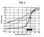
Fig. 4 is a graph showing a relationship between a heating temperature and a film stress of the silicon oxide film formed by plasma CVD. -
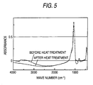
Fig. 5 is a diagram showing an infrared absorption spectrum of a silicon oxide film before heat treatment and after heat treatment. -
- 1: membrane
- 2: substrate
- 3: silicon oxide film
- 6: Pt/Ti wiring element (electronic element)
- 13: heat-shrinkable silicon oxide film
- Hereinafter, a membrane structure element according to one embodiment of this invention will be described together with a manufacturing method thereof. Shown in
Figs. 2(1) and 2(2) is the membrane structure element according to the embodiment, and the element is provided with amembrane 1 which is formed of asilicon oxide film 3 and has a square shape as viewed in plane view; and asilicon substrate 2 in which thesilicon oxide film 3 having the same film constitution as that of the silicon oxide film constituting themembrane 1 is laminated on the surface thereof. Themembrane 1 is supported on arecessed part 4 provided on thesubstrate 2 in a hollow state and a flat shape by foursupport arms 5. Themembrane 1, the supportarms 5, and thesilicon oxide film 3 on the substrate are integrally formed so that thesupport arms 5 connect four corners of themembrane 1 and thesubstrate 2. A Pt/Ti wiring element 6 which constitutes a detection electronic element and has two layer structure lines of a Pt layer and a Ti layer disposed as being bent upward and downward is formed on a surface of themembrane 1 by laminating. - Hereinafter, the manufacturing method for the membrane structure element according to the above-described embodiment will be described with reference to
Figs. 1(1) through 1(4) . A general purpose silicon substrate (single crystal silicon substrate having a crystal orientation of (100)) 2 is prepared, and considerably thin heat oxidizedsilicon oxide films substrate 2 as shown inFig. 1(1) . The heat oxidizedsilicon oxide film 12 on the back surface is formed for the purpose of protection of the back surface of the silicon substrate when etching the silicon substrate in a subsequent step. The heat oxidizedsilicon oxide film 11 on the front surface is basically not necessary. Therefore, the heat oxidizedsilicon oxide film 11 on the front surface may be removed after the film formation, or it is possible to omit the formation of heat oxidized silicon oxide films on the front and back surfaces by providing an appropriate protection film on the back surface of the substrate. Since a compression stress of about 200 MPa remains in the heat oxidized silicon oxide film, it is preferable that the heat oxidizedsilicon oxide film 11 does not exist on the front surface. However, the heat oxidizedsilicon oxide film 11 is considerably thin (about 0.1 µm), and it is possible to ignore influences to be exerted on the remaining stress by sufficiently increasing a thickness of a heat-shrinkablesilicon oxide film 13 as compared to the heat oxidizedsilicon oxide film 11. Therefore, the heat oxidizedsilicon oxide film 11 on the front surface is left as it is in this embodiment. - Next, as shown in
Fig. 1(2) , the heat-shrinkablesilicon oxide film 13 is formed on the front surface of the heat oxidizedsilicon oxide film 11. This step is called a film formation step. A thickness of the heat-shrinkable silicon oxide film may be set within a range of from 0.1 to 10 µm from the view point of strength and heat insulating property of the film. In the case of forming the heat oxidizedsilicon oxide film 11, it is recommendable to set the thickness to five times or more that of the heat oxidized silicon oxide film. Note that the heat oxidizedsilicon oxide film 11 on the front surface and the heat-shrinkablesilicon oxide film 13 are not particularly discriminated, and they are referred to as thesilicon oxide film 3. - As a film formation method for the heat-shrinkable
silicon oxide film 13, plasma CVD method is the optimum method in view of its film formation speed and easiness of film formation. Hereinafter, an input power for plasma in the case of forming the silicon oxide film by plasma CVD method and a stress remaining in the film will be described. - A silicon oxide film was formed by the following procedure. A silicon substrate (thickness: 525 µm) on which the heat oxidized silicon oxide film 11 (film thickness: 0.1 µm) had been formed was prepared, and a silicon oxide film having a film thickness of 1 µm was formed thereon by plasma CVD method. Each of a platform and an electrode opposed to the platform of a plasma CVD apparatus used for the film formation had a diameter of 30 cm (surface area: about 707 cm2). Various silicon oxide films were formed under the film formation conditions in which a mixture gas of SiH4, N2, N2O was used, a gas pressure was set to 80 Pa, a substrate temperature was set at 200°C or 300°C, and input powers for plasma were varied.
- After the film formation, film remaining stresses were measured using the respective silicon oxide films. The film remaining stress was detected based on a warping amount of the substrate and in accordance with the following formula. As the warping amount, a value measured at a room temperature (23 °C) was used. The warping amount of the substrate was measured using reflections of laser beams or a probe type surface roughness meter while supporting three points of the substrate (diameter: 100 mmφ).

- In this formula, E is Young's modules of the substrate (silicon), ν is a Poisson's ratio of the substrate (silicon), Rpost is a radius of curvature of warping of the substrate after film formation, Rpre is a radius of curvature of warping of the substrate before film formation, ts is a thickness of the substrate, tf is a thickness of the film, and a value of E/(1-ν) is 1.8 × 10¹¹ Pa in the case of the single crystal silicon (100) substrate.
- Shown in
Fig. 3 is a relationship between the input power for plasma and the stress remaining in the film detected as described above. According to this figure, the remaining stress of the film is -300 MPa (compression) when the substrate temperature is 300°C and the input power is 100 W, for example, and it is apparent that the internal stress after the film formation is reduced in absolute value along with an increase in input power. It is revealed that the remaining stress of the silicon oxide film after the film formation is a compression stress from the fact that the substrate after the film formation is warped with the silicon oxide film surface being projected. Also, it is revealed that the remaining stress is alleviated when the substrate temperature is 200°C in comparison with the case that the substrate temperature is 300°C. - Subsequently, the substrate on which the heat-shrinkable silicon oxide film is formed is subjected to a heat treatment to cause the heat shrinkage of the heat-shrinkable
silicon oxide film 13, thereby alleviate or resolve the internal compression remaining stress of thesilicon oxide film 13. This step is called a heat treatment step. - Hereinafter, the action of the heat treatment for alleviating the compression remaining stress will be described in detail. By using a silicon substrate on which a silicon oxide film was formed at a substrate temperature of 300°C and with an input power for plasma CVD of 200 W, an internal stress with respect to a heating temperature when heating the silicon substrate in a nitrogen gas atmosphere was measured. The results are shown in
Fig. 4 . Heating of the silicon oxide film was performed by inserting the silicon substrate on which the silicon oxide film was formed into a heating furnace in such a manner that a temperature of the silicon substrate and a in-furnace ambient temperature which was controlled to a measurement temperature were substantially the same and that a retention time at the measurement temperature was set to 1 hour. A measurement device used for the measurement was type-F2410 manufactured by KLA-Tencor. - According to
Fig. 4 , substantially no change was observed until around 400°C with the stress that was -200 MPa before the heat processing, and then the stress sharply changed between 400°C and 700°C (changed to the positive value). It is considered that the internal stress changed to the positive value (stretching stress) since the film was densified to shrink a little due to a reaction of non-bonding hands in the silicon oxide film in the temperature region. The inclination of the curvature was reduced between 700°C and 800°C, and the stress was reduced almost linearly when the temperature was lowered ultimately reaching to a value of about -80 MPa at a room temperature. From the results, it is revealed that the heating temperature in the heat treatment may preferably be 400°C or more. It is also revealed that, although the heating may be performed at about 1000°C more, the heating temperature may preferably be 800°C or less, more preferably 700°C or less. - A heat treatment in a nitrogen gas at 800°C for 1 hour was performed on the substrates on each of which a silicon oxide film was formed by the above-described plasma CVD method with changing the input power. As to the stress after the heat treatment, it is revealed that the stress alleviating effect of the film formed with the reduced input power is greater as shown in
Fig. 3 . Further, the heat-shrinkable silicon oxide film formed at the substrate temperature of 300°C achieved the internal stress of substantially 0 at the input power of 75 W, and the average internal stress was reduced to about -50 MPa. Moreover, the remaining stress of the heat-shrinkable silicon oxide film formed at the substrate temperature of 200°C with the input power of 75 to 150 W (0.11 to 0.21 W/cm2) is 0 to +50 MPa which means that the internal stress is a stretching stress. - Furthermore, according to
Fig. 3 , it is proved that the film remaining stress alleviating effect by the heat treatment is increased to make the stress adjustment easier when the input power is smaller and the substrate temperature is lower. In order to perform adjustment to the appropriate stress range depending on the material of the substrate and the thickness of the heat-shrinkable silicon oxide film, the adjustment of the input power and the substrate temperature is considered to be effective as described above. In the case of forming the film having the thickness of about 1 µm that is appropriate for the application of this invention on the single crystal substrate, as is apparent fromFig. 3 , it is possible to adjust the film remaining stress to about -100 MPa or less by setting the substrate temperature to 300°C or less and the input power to 250 W (0.35 W/cm2) or less, and it is possible to adjust the film remaining stress to about -50 MPa or less by setting the substrate temperature to 300°C or less and the input power to 150 W (0.21 W/cm2) or less. Further, it is possible to adjust the film remaining stress to the stretching stress of about 0 to +50 MPa by setting the substrate temperature to 200°C or less and the input power to 150 W (0.21 W/cm2) or less. From the view point of ensuring stability of the film formation by plasma CVD method, it is preferable to set the input power to 50 W (0.07 W/cm2) or more and the substrate temperature to 100°C or more. - Further, the stress alleviating effect by the heat treatment was confirmed from the view point of framework by the following investigation. A bonding state of silicon oxides of each of a heat-shrinkable silicon oxide film after film formation (before heat treatment) and the silicon oxide film after heat treatment was examined by Fourier transformation infrared spectroscopy (FTIR). As one example, shown in
Fig. 5 is an infrared absorption spectrum of the film obtained at the substrate temperature of 200°C and the input power of 75 W shown inFig. 3 . FromFig. 5 , it is proved that absorption bands by Si-OH bonds and H2O observed at a wave number of 300 to 3700 cm-1 and near 950 cm-1 disappear due to the heat treatment, and that a dominant band of silicon oxides near 1070 cm-1 shows tendency of increase. That is, the silicon oxide film is changed from the state in which many imperfect bonds are present to the more dense silicon oxide film by the heat treatment. Accordingly, it is considered that the film is shrunk by the heat treatment to be changed into a stretching stress state. - Subsequently, as shown in
Fig. 1(3) , a Pt/Ti wiring element having a predetermined pattern is formed by a lift-off method or the like on thesilicon oxide film 3 after the heat treatment. Although necessary wiring patterns are formed on thesilicon oxide film 3 in addition to the detection element wiring pattern, such wiring patterns are omitted in the drawings. This step is called an element formation step. - Subsequently, in order to make the vicinity of a silicon oxide film part (membrane-corresponding part) including the Pt/Ti wiring element in a hollow structure, silicon of the
substrate 2 below the membrane-corresponding part is removed. This step is called a removal step. More specifically, as shown inFig. 1(4) , anopening 14 is formed around the membrane-corresponding part by removing thesilicon oxide film 3 by the use of a chemical or physical means while avoiding parts corresponding to thesupport arms 5 of the membrane 1 (seeFigs. 2(1) and 2(2) ). After that, thesubstrate 2 is impregnated into an etching liquid to perform etching on silicon of thesubstrate 2 exposed inside theopening 14. At this time, silicon is subjected to anisotropic etching that depends on the crystal orientation, so that the recessedpart 4 penetrating in a horizontal direction below the membrane-corresponding part is easily formed. As the etching liquid, for example, a TMAH (tetramethylammonium hydroxide) solution heated to about 80°C is used. After forming the recessedpart 4, the etching liquid is washed off so as not to break the membrane, followed by drying, to thereby complete the membrane structure element shown inFig. 2 . - Among the thus-manufactured membrane structure elements, each of those formed at the substrate temperature of 300°C and with the input power in the plasma CVD of 100 W or 200 W (each the stresses of the
silicon oxide films 3 after the film formation was -300 MPa or -200 MPa) was subjected to a measurement of a maximum deflection amount (distance from the surface of thesilicon oxide film 3 of the substrate as a reference surface to a surface of a maximum deflection part of the membrane) of the membrane supported in the hollow state at a room temperature, and a ratio of the maximum deflection amount to the maximum width of the membrane was detected. The maximum deflection amount of the membrane was measured by employing an optical method. More specifically, the measurement was conducted by employing a height measurement function of a microscope. As a result, the one formed with the input power of 100 W achieved the ratio of 0.05%, and the one formed with the input power of 200 W achieved the ratio of 0.1 %, thereby ensuring that the membranes are supported by the substrate in a remarkably flat shape. - When a current is supplied to the Pt/Ti wiring element in the membrane structure element having the above-described hollow structure, the temperature is easily increased due to the heat insulating property and heat capacity of the membrane structure, and, in the case where the membrane structure element is used for an air flow sensor or the like, it is possible to detect from a change in resistance of the Pt/Ti detection element an air flow amount associated with a speed at which the heat is drawn from the hollow structure.
- Although the heat-shrinkable
silicon oxide film 13 is formed by plasma CVD method in the film formation method in the above embodiment, it is possible to employ any method that is capable of forming the silicon oxide film having a lower density than that of the heat oxidized silicon oxide film, such as PVD method including sputtering and vapor deposition, and a sol/gel method, without limitation to the plasma CVD method. Further, although the single crystal silicon substrate is used as the substrate in the above-described embodiment, it is possible to use other crystals, a ceramic, a resin, or the like without limitation to the single crystal silicon substrate. - Moreover, because of the easiness of the manufacture of the membrane excellent in hollowness and flatness, the film formation step, the heat treatment step, the element formation step, and the removal step are performed in this order in the above-described embodiment, it is possible to form a silicon oxide film on a wiring element after forming the wiring element on a silicon oxide film so as to enclose the wiring element with the silicon oxide films (the films are present below and above the element) insofar as the element formation step is performed in advance of the removal step. Further, the heat treatment step and the removing step may be exchanged in the case where the element forming step is not performed.
Claims (10)
- A method for manufacturing a membrane structure element comprising a membrane formed of a silicon oxide film and a substrate which supports the membrane in a hollow state by supporting a part of a periphery of the membrane, said method comprising:a film formation step of forming a heat-shrinkable silicon oxide film on a surface of a substrate formed of a material having a heat expansion coefficient that is higher than a heat expansion coefficient of silicon oxide;a heat treatment step of heating the heat-shrinkable silicon oxide film to cause a heat shrinkage of said film; anda removal step of removing a part of the substrate in the form of a recess so that a corresponding part of the silicon oxide film corresponding to the membrane is supported as the membrane in a hollow state with respect to the substrate.
- The method for manufacturing a membrane structure element according to claim 1, which comprises an element formation step of forming a metal wiring having a predetermined pattern on a surface of the silicon oxide film.
- The method for manufacturing a membrane structure element according to claim 1 or 2, wherein the heat-shrinkable silicon oxide is formed by plasma CVD method.
- The method for manufacturing a membrane structure element according to claim 3, wherein a silane gas is used as a film-formation raw material gas; and a substrate temperature is set at 200°C or less and an input power is set to 0.21 W/cm2 or less during the film formation.
- The method for manufacturing a membrane structure element according to any one of claims 1 to 4, wherein the heating is performed at a temperature of 400°C or more in the heat treatment step.
- The method for manufacturing a membrane structure element according to any one of claims 1 to 5, wherein the heat-shrinkable silicon oxide film is heated together with the substrate in the heat treatment step so that an internal stress of the silicon oxide film becomes within a stress range of stretching of (+)100 MPa to compression of (-)100 MPa.
- The method for manufacturing a membrane structure element according to any one of claims 1 to 6, wherein the substrate comprises a single crystal silicon; and a part of the substrate is removed by silicon anisotropic etching in the removal step.
- A membrane structure element obtained by the method according to any one of claims 1 to 7, said membrane structure element comprising a membrane formed of a silicon oxide film and a substrate which supports the membrane in a hollow state by supporting a part of a periphery of the membrane.
- A membrane structure element, comprising a membrane formed of a silicon oxide film and a substrate which supports the membrane in a hollow state by supporting a part of a periphery of the membrane, wherein the silicon oxide film is supported in a flat shape due to a heat shrinkage.
- The membrane structure element according to claim 9, wherein a maximum deflection amount of the membrane is 0.1 % or less of a maximum width of the membrane when a surface of the silicon oxide film which is formed on the surface of the substrate and has an identical constitution with the membrane is taken as a reference surface.
Applications Claiming Priority (2)
| Application Number | Priority Date | Filing Date | Title |
|---|---|---|---|
| JP2006087090 | 2006-03-28 | ||
| PCT/JP2007/056723 WO2007114191A1 (en) | 2006-03-28 | 2007-03-28 | Membrane structure element and method for manufacturing same |
Publications (4)
| Publication Number | Publication Date |
|---|---|
| EP2001062A2 true EP2001062A2 (en) | 2008-12-10 |
| EP2001062A9 EP2001062A9 (en) | 2009-04-08 |
| EP2001062A4 EP2001062A4 (en) | 2012-03-28 |
| EP2001062B1 EP2001062B1 (en) | 2013-12-11 |
Family
ID=38563460
Family Applications (1)
| Application Number | Title | Priority Date | Filing Date |
|---|---|---|---|
| EP07740161.0A Not-in-force EP2001062B1 (en) | 2006-03-28 | 2007-03-28 | Method for manufacturing a membrane structure element |
Country Status (5)
| Country | Link |
|---|---|
| US (1) | US8057882B2 (en) |
| EP (1) | EP2001062B1 (en) |
| KR (1) | KR20080097243A (en) |
| CN (1) | CN101410999A (en) |
| WO (1) | WO2007114191A1 (en) |
Families Citing this family (7)
| Publication number | Priority date | Publication date | Assignee | Title |
|---|---|---|---|---|
| JP4888908B2 (en) * | 2007-10-17 | 2012-02-29 | 株式会社神戸製鋼所 | Membrane structure element and manufacturing method thereof |
| US9214604B2 (en) * | 2010-01-21 | 2015-12-15 | Cambridge Cmos Sensors Limited | Plasmonic IR devices |
| CN102234099B (en) * | 2010-05-06 | 2015-09-16 | 哈尔滨佳启科技开发有限公司 | Gas sensor forced ventilation cold-heat pump micro Process manufacture method |
| US11008627B2 (en) | 2019-08-15 | 2021-05-18 | Talis Biomedical Corporation | Diagnostic system |
| JP6807005B2 (en) * | 2019-12-25 | 2021-01-06 | ミツミ電機株式会社 | Flow sensor |
| US12169137B2 (en) * | 2020-03-10 | 2024-12-17 | Hitachi Astemo, Ltd. | Airflow amount measuring device |
| CN114964400B (en) * | 2022-06-14 | 2023-06-30 | 南京高华科技股份有限公司 | Flow sensor and manufacturing method thereof |
Family Cites Families (10)
| Publication number | Priority date | Publication date | Assignee | Title |
|---|---|---|---|---|
| JP3049796B2 (en) | 1991-03-15 | 2000-06-05 | 富士通株式会社 | Method of forming insulating film |
| JP2994881B2 (en) | 1992-10-22 | 1999-12-27 | 松下電工株式会社 | Thermal insulation film for diaphragm structure and method of manufacturing the same |
| JP3833274B2 (en) | 1993-06-10 | 2006-10-11 | 三菱電機株式会社 | X-ray mask manufacturing method |
| JPH08264844A (en) | 1995-03-24 | 1996-10-11 | Nippondenso Co Ltd | Floating membrane |
| JPH09306812A (en) | 1996-05-15 | 1997-11-28 | Nec Corp | Manufacture of x-ray mask |
| JPH11274067A (en) | 1998-01-21 | 1999-10-08 | Mitsubishi Electric Corp | X-ray mask stress adjustment method |
| JP4046014B2 (en) | 2003-05-30 | 2008-02-13 | 株式会社デンソー | Manufacturing method of structure |
| JP3968524B2 (en) * | 2004-02-04 | 2007-08-29 | ソニー株式会社 | Mask, exposure method and semiconductor device manufacturing method |
| JP4547974B2 (en) | 2004-04-26 | 2010-09-22 | 株式会社デンソー | Flow sensor and manufacturing method thereof |
| JP2006030159A (en) * | 2004-06-15 | 2006-02-02 | Canon Inc | Piezoresistive semiconductor device and manufacturing method thereof |
-
2007
- 2007-03-28 US US12/225,670 patent/US8057882B2/en not_active Expired - Fee Related
- 2007-03-28 EP EP07740161.0A patent/EP2001062B1/en not_active Not-in-force
- 2007-03-28 KR KR1020087023570A patent/KR20080097243A/en not_active Ceased
- 2007-03-28 WO PCT/JP2007/056723 patent/WO2007114191A1/en not_active Ceased
- 2007-03-28 CN CNA2007800115520A patent/CN101410999A/en active Pending
Non-Patent Citations (2)
| Title |
|---|
| No further relevant documents disclosed * |
| See also references of WO2007114191A1 * |
Also Published As
| Publication number | Publication date |
|---|---|
| KR20080097243A (en) | 2008-11-04 |
| US20090176064A1 (en) | 2009-07-09 |
| EP2001062A9 (en) | 2009-04-08 |
| WO2007114191A1 (en) | 2007-10-11 |
| EP2001062B1 (en) | 2013-12-11 |
| US8057882B2 (en) | 2011-11-15 |
| CN101410999A (en) | 2009-04-15 |
| EP2001062A4 (en) | 2012-03-28 |
Similar Documents
| Publication | Publication Date | Title |
|---|---|---|
| EP2001062B1 (en) | Method for manufacturing a membrane structure element | |
| US20090029048A1 (en) | Method of thermal stress compensation | |
| EP1826174A2 (en) | Method for forming thin film structure having small tensile stress | |
| JPS60105216A (en) | Manufacture of thin film semiconductor device | |
| JP4888908B2 (en) | Membrane structure element and manufacturing method thereof | |
| JP4780671B2 (en) | Membrane structure element and manufacturing method thereof | |
| RU2059321C1 (en) | Method for producing flexible parts from single-crystalline silicon | |
| TWI288454B (en) | Wafer carrier having improved processing characteristics | |
| JPH09148467A (en) | Structure for vacuum-sealing working element and its manufacture | |
| Chou et al. | Fabrication of low-stress dielectric thin-film for microsensor applications | |
| Ababneh et al. | Investigations on the high temperature compatibility of various adhesion layers for platinum | |
| JP2010204029A (en) | Hollow structure element | |
| CN216698280U (en) | Low stress dielectric composite film | |
| Chang et al. | Micromechanical structures in amorphous silicon | |
| JPH06112509A (en) | Manufacture of micromachine | |
| Cheng et al. | Ultralow-stress silicon-rich nitride films for microstructure fabrication | |
| JP2008084991A (en) | Thermistor thin film and thin film thermistor element | |
| JP2005086086A (en) | CVD apparatus and semiconductor device manufacturing method | |
| Long et al. | Modeling and extraction of residual stresses in MEMS multilayer systems | |
| JP2003017767A (en) | Piezoelectric element | |
| JP2004311624A (en) | Laminate and manufacturing method thereof | |
| TW418475B (en) | Configuration method for thin film cracking parameters and the application using the same | |
| JP2008048315A (en) | Piezoelectric vibrating piece and manufacturing method thereof | |
| JPH04192566A (en) | Semiconductor device and its manufacture | |
| KR101177275B1 (en) | Degassing method of a thin layer and manufacturing method of Si film |
Legal Events
| Date | Code | Title | Description |
|---|---|---|---|
| PUAI | Public reference made under article 153(3) epc to a published international application that has entered the european phase |
Free format text: ORIGINAL CODE: 0009012 |
|
| 17P | Request for examination filed |
Effective date: 20081002 |
|
| AK | Designated contracting states |
Kind code of ref document: A2 Designated state(s): AT BE BG CH CY CZ DE DK EE ES FI FR GB GR HU IE IS IT LI LT LU LV MC MT NL PL PT RO SE SI SK TR |
|
| PUAB | Information related to the publication of an a document modified or deleted |
Free format text: ORIGINAL CODE: 0009199EPPU |
|
| A4 | Supplementary search report drawn up and despatched |
Effective date: 20120223 |
|
| RIC1 | Information provided on ipc code assigned before grant |
Ipc: H01L 37/00 20060101ALI20120217BHEP Ipc: G01F 1/692 20060101ALI20120217BHEP Ipc: C23C 16/42 20060101ALI20120217BHEP Ipc: H01L 35/34 20060101ALI20120217BHEP Ipc: B81C 1/00 20060101AFI20120217BHEP Ipc: G01J 1/02 20060101ALI20120217BHEP |
|
| DAX | Request for extension of the european patent (deleted) | ||
| 17Q | First examination report despatched |
Effective date: 20130204 |
|
| REG | Reference to a national code |
Ref country code: DE Ref legal event code: R079 Ref document number: 602007034205 Country of ref document: DE Free format text: PREVIOUS MAIN CLASS: H01L0037000000 Ipc: B81C0001000000 |
|
| GRAP | Despatch of communication of intention to grant a patent |
Free format text: ORIGINAL CODE: EPIDOSNIGR1 |
|
| RIC1 | Information provided on ipc code assigned before grant |
Ipc: C23C 16/56 20060101ALI20130627BHEP Ipc: H01L 37/00 20060101ALI20130627BHEP Ipc: G01J 1/02 20060101ALI20130627BHEP Ipc: H01L 35/34 20060101ALI20130627BHEP Ipc: G01F 1/692 20060101ALI20130627BHEP Ipc: C23C 16/40 20060101ALI20130627BHEP Ipc: B81C 1/00 20060101AFI20130627BHEP |
|
| INTG | Intention to grant announced |
Effective date: 20130723 |
|
| GRAS | Grant fee paid |
Free format text: ORIGINAL CODE: EPIDOSNIGR3 |
|
| GRAA | (expected) grant |
Free format text: ORIGINAL CODE: 0009210 |
|
| RIN1 | Information on inventor provided before grant (corrected) |
Inventor name: HIRANO, TAKAYUKI Inventor name: KAWAKAMI, NOBUYUKI Inventor name: KANNAKA, MASATO |
|
| AK | Designated contracting states |
Kind code of ref document: B1 Designated state(s): AT BE BG CH CY CZ DE DK EE ES FI FR GB GR HU IE IS IT LI LT LU LV MC MT NL PL PT RO SE SI SK TR |
|
| REG | Reference to a national code |
Ref country code: GB Ref legal event code: FG4D |
|
| REG | Reference to a national code |
Ref country code: CH Ref legal event code: EP Ref country code: CH Ref legal event code: NV Representative=s name: E. BLUM AND CO. AG PATENT- UND MARKENANWAELTE , CH |
|
| REG | Reference to a national code |
Ref country code: AT Ref legal event code: REF Ref document number: 644475 Country of ref document: AT Kind code of ref document: T Effective date: 20140115 |
|
| REG | Reference to a national code |
Ref country code: IE Ref legal event code: FG4D |
|
| REG | Reference to a national code |
Ref country code: DE Ref legal event code: R096 Ref document number: 602007034205 Country of ref document: DE Effective date: 20140206 |
|
| REG | Reference to a national code |
Ref country code: NL Ref legal event code: VDEP Effective date: 20131211 |
|
| REG | Reference to a national code |
Ref country code: AT Ref legal event code: MK05 Ref document number: 644475 Country of ref document: AT Kind code of ref document: T Effective date: 20131211 |
|
| PG25 | Lapsed in a contracting state [announced via postgrant information from national office to epo] |
Ref country code: SE Free format text: LAPSE BECAUSE OF FAILURE TO SUBMIT A TRANSLATION OF THE DESCRIPTION OR TO PAY THE FEE WITHIN THE PRESCRIBED TIME-LIMIT Effective date: 20131211 Ref country code: FI Free format text: LAPSE BECAUSE OF FAILURE TO SUBMIT A TRANSLATION OF THE DESCRIPTION OR TO PAY THE FEE WITHIN THE PRESCRIBED TIME-LIMIT Effective date: 20131211 Ref country code: NL Free format text: LAPSE BECAUSE OF FAILURE TO SUBMIT A TRANSLATION OF THE DESCRIPTION OR TO PAY THE FEE WITHIN THE PRESCRIBED TIME-LIMIT Effective date: 20131211 Ref country code: LT Free format text: LAPSE BECAUSE OF FAILURE TO SUBMIT A TRANSLATION OF THE DESCRIPTION OR TO PAY THE FEE WITHIN THE PRESCRIBED TIME-LIMIT Effective date: 20131211 |
|
| REG | Reference to a national code |
Ref country code: LT Ref legal event code: MG4D |
|
| PG25 | Lapsed in a contracting state [announced via postgrant information from national office to epo] |
Ref country code: AT Free format text: LAPSE BECAUSE OF FAILURE TO SUBMIT A TRANSLATION OF THE DESCRIPTION OR TO PAY THE FEE WITHIN THE PRESCRIBED TIME-LIMIT Effective date: 20131211 Ref country code: CY Free format text: LAPSE BECAUSE OF FAILURE TO SUBMIT A TRANSLATION OF THE DESCRIPTION OR TO PAY THE FEE WITHIN THE PRESCRIBED TIME-LIMIT Effective date: 20131211 Ref country code: LV Free format text: LAPSE BECAUSE OF FAILURE TO SUBMIT A TRANSLATION OF THE DESCRIPTION OR TO PAY THE FEE WITHIN THE PRESCRIBED TIME-LIMIT Effective date: 20131211 |
|
| PG25 | Lapsed in a contracting state [announced via postgrant information from national office to epo] |
Ref country code: BE Free format text: LAPSE BECAUSE OF FAILURE TO SUBMIT A TRANSLATION OF THE DESCRIPTION OR TO PAY THE FEE WITHIN THE PRESCRIBED TIME-LIMIT Effective date: 20131211 Ref country code: IS Free format text: LAPSE BECAUSE OF FAILURE TO SUBMIT A TRANSLATION OF THE DESCRIPTION OR TO PAY THE FEE WITHIN THE PRESCRIBED TIME-LIMIT Effective date: 20140411 Ref country code: EE Free format text: LAPSE BECAUSE OF FAILURE TO SUBMIT A TRANSLATION OF THE DESCRIPTION OR TO PAY THE FEE WITHIN THE PRESCRIBED TIME-LIMIT Effective date: 20131211 |
|
| PG25 | Lapsed in a contracting state [announced via postgrant information from national office to epo] |
Ref country code: CZ Free format text: LAPSE BECAUSE OF FAILURE TO SUBMIT A TRANSLATION OF THE DESCRIPTION OR TO PAY THE FEE WITHIN THE PRESCRIBED TIME-LIMIT Effective date: 20131211 Ref country code: PT Free format text: LAPSE BECAUSE OF FAILURE TO SUBMIT A TRANSLATION OF THE DESCRIPTION OR TO PAY THE FEE WITHIN THE PRESCRIBED TIME-LIMIT Effective date: 20140411 Ref country code: ES Free format text: LAPSE BECAUSE OF FAILURE TO SUBMIT A TRANSLATION OF THE DESCRIPTION OR TO PAY THE FEE WITHIN THE PRESCRIBED TIME-LIMIT Effective date: 20131211 Ref country code: PL Free format text: LAPSE BECAUSE OF FAILURE TO SUBMIT A TRANSLATION OF THE DESCRIPTION OR TO PAY THE FEE WITHIN THE PRESCRIBED TIME-LIMIT Effective date: 20131211 Ref country code: SK Free format text: LAPSE BECAUSE OF FAILURE TO SUBMIT A TRANSLATION OF THE DESCRIPTION OR TO PAY THE FEE WITHIN THE PRESCRIBED TIME-LIMIT Effective date: 20131211 Ref country code: RO Free format text: LAPSE BECAUSE OF FAILURE TO SUBMIT A TRANSLATION OF THE DESCRIPTION OR TO PAY THE FEE WITHIN THE PRESCRIBED TIME-LIMIT Effective date: 20131211 |
|
| REG | Reference to a national code |
Ref country code: DE Ref legal event code: R097 Ref document number: 602007034205 Country of ref document: DE |
|
| PLBE | No opposition filed within time limit |
Free format text: ORIGINAL CODE: 0009261 |
|
| STAA | Information on the status of an ep patent application or granted ep patent |
Free format text: STATUS: NO OPPOSITION FILED WITHIN TIME LIMIT |
|
| PG25 | Lapsed in a contracting state [announced via postgrant information from national office to epo] |
Ref country code: LU Free format text: LAPSE BECAUSE OF FAILURE TO SUBMIT A TRANSLATION OF THE DESCRIPTION OR TO PAY THE FEE WITHIN THE PRESCRIBED TIME-LIMIT Effective date: 20140328 Ref country code: DK Free format text: LAPSE BECAUSE OF FAILURE TO SUBMIT A TRANSLATION OF THE DESCRIPTION OR TO PAY THE FEE WITHIN THE PRESCRIBED TIME-LIMIT Effective date: 20131211 |
|
| 26N | No opposition filed |
Effective date: 20140912 |
|
| GBPC | Gb: european patent ceased through non-payment of renewal fee |
Effective date: 20140328 |
|
| REG | Reference to a national code |
Ref country code: DE Ref legal event code: R097 Ref document number: 602007034205 Country of ref document: DE Effective date: 20140912 |
|
| REG | Reference to a national code |
Ref country code: FR Ref legal event code: ST Effective date: 20141128 |
|
| REG | Reference to a national code |
Ref country code: IE Ref legal event code: MM4A |
|
| PG25 | Lapsed in a contracting state [announced via postgrant information from national office to epo] |
Ref country code: IE Free format text: LAPSE BECAUSE OF NON-PAYMENT OF DUE FEES Effective date: 20140328 Ref country code: GB Free format text: LAPSE BECAUSE OF NON-PAYMENT OF DUE FEES Effective date: 20140328 Ref country code: FR Free format text: LAPSE BECAUSE OF NON-PAYMENT OF DUE FEES Effective date: 20140331 |
|
| PG25 | Lapsed in a contracting state [announced via postgrant information from national office to epo] |
Ref country code: SI Free format text: LAPSE BECAUSE OF FAILURE TO SUBMIT A TRANSLATION OF THE DESCRIPTION OR TO PAY THE FEE WITHIN THE PRESCRIBED TIME-LIMIT Effective date: 20131211 |
|
| PGFP | Annual fee paid to national office [announced via postgrant information from national office to epo] |
Ref country code: DE Payment date: 20150324 Year of fee payment: 9 Ref country code: CH Payment date: 20150313 Year of fee payment: 9 |
|
| PG25 | Lapsed in a contracting state [announced via postgrant information from national office to epo] |
Ref country code: MT Free format text: LAPSE BECAUSE OF FAILURE TO SUBMIT A TRANSLATION OF THE DESCRIPTION OR TO PAY THE FEE WITHIN THE PRESCRIBED TIME-LIMIT Effective date: 20131211 |
|
| PG25 | Lapsed in a contracting state [announced via postgrant information from national office to epo] |
Ref country code: MC Free format text: LAPSE BECAUSE OF FAILURE TO SUBMIT A TRANSLATION OF THE DESCRIPTION OR TO PAY THE FEE WITHIN THE PRESCRIBED TIME-LIMIT Effective date: 20131211 Ref country code: BG Free format text: LAPSE BECAUSE OF FAILURE TO SUBMIT A TRANSLATION OF THE DESCRIPTION OR TO PAY THE FEE WITHIN THE PRESCRIBED TIME-LIMIT Effective date: 20131211 |
|
| PG25 | Lapsed in a contracting state [announced via postgrant information from national office to epo] |
Ref country code: GR Free format text: LAPSE BECAUSE OF FAILURE TO SUBMIT A TRANSLATION OF THE DESCRIPTION OR TO PAY THE FEE WITHIN THE PRESCRIBED TIME-LIMIT Effective date: 20140312 Ref country code: IT Free format text: LAPSE BECAUSE OF FAILURE TO SUBMIT A TRANSLATION OF THE DESCRIPTION OR TO PAY THE FEE WITHIN THE PRESCRIBED TIME-LIMIT Effective date: 20131211 |
|
| PG25 | Lapsed in a contracting state [announced via postgrant information from national office to epo] |
Ref country code: HU Free format text: LAPSE BECAUSE OF FAILURE TO SUBMIT A TRANSLATION OF THE DESCRIPTION OR TO PAY THE FEE WITHIN THE PRESCRIBED TIME-LIMIT; INVALID AB INITIO Effective date: 20070328 Ref country code: TR Free format text: LAPSE BECAUSE OF FAILURE TO SUBMIT A TRANSLATION OF THE DESCRIPTION OR TO PAY THE FEE WITHIN THE PRESCRIBED TIME-LIMIT Effective date: 20131211 |
|
| REG | Reference to a national code |
Ref country code: DE Ref legal event code: R119 Ref document number: 602007034205 Country of ref document: DE |
|
| REG | Reference to a national code |
Ref country code: CH Ref legal event code: PL |
|
| PG25 | Lapsed in a contracting state [announced via postgrant information from national office to epo] |
Ref country code: LI Free format text: LAPSE BECAUSE OF NON-PAYMENT OF DUE FEES Effective date: 20160331 Ref country code: DE Free format text: LAPSE BECAUSE OF NON-PAYMENT OF DUE FEES Effective date: 20161001 Ref country code: CH Free format text: LAPSE BECAUSE OF NON-PAYMENT OF DUE FEES Effective date: 20160331 |