EP1998214A1 - Lighting device - Google Patents
Lighting device Download PDFInfo
- Publication number
- EP1998214A1 EP1998214A1 EP07010692A EP07010692A EP1998214A1 EP 1998214 A1 EP1998214 A1 EP 1998214A1 EP 07010692 A EP07010692 A EP 07010692A EP 07010692 A EP07010692 A EP 07010692A EP 1998214 A1 EP1998214 A1 EP 1998214A1
- Authority
- EP
- European Patent Office
- Prior art keywords
- lighting device
- light sources
- optics
- fresnel
- secondary optics
- Prior art date
- Legal status (The legal status is an assumption and is not a legal conclusion. Google has not performed a legal analysis and makes no representation as to the accuracy of the status listed.)
- Granted
Links
- 230000005855 radiation Effects 0.000 claims abstract description 36
- 238000000034 method Methods 0.000 claims abstract description 6
- 238000004519 manufacturing process Methods 0.000 claims abstract description 4
- 230000003287 optical effect Effects 0.000 claims description 24
- 238000000926 separation method Methods 0.000 description 6
- 238000004088 simulation Methods 0.000 description 2
- 238000003491 array Methods 0.000 description 1
- 150000001875 compounds Chemical class 0.000 description 1
- 230000002596 correlated effect Effects 0.000 description 1
- 230000000694 effects Effects 0.000 description 1
- 238000003384 imaging method Methods 0.000 description 1
- 239000000758 substrate Substances 0.000 description 1
Images



Classifications
-
- F—MECHANICAL ENGINEERING; LIGHTING; HEATING; WEAPONS; BLASTING
- F21—LIGHTING
- F21V—FUNCTIONAL FEATURES OR DETAILS OF LIGHTING DEVICES OR SYSTEMS THEREOF; STRUCTURAL COMBINATIONS OF LIGHTING DEVICES WITH OTHER ARTICLES, NOT OTHERWISE PROVIDED FOR
- F21V5/00—Refractors for light sources
- F21V5/04—Refractors for light sources of lens shape
- F21V5/045—Refractors for light sources of lens shape the lens having discontinuous faces, e.g. Fresnel lenses
-
- F—MECHANICAL ENGINEERING; LIGHTING; HEATING; WEAPONS; BLASTING
- F21—LIGHTING
- F21V—FUNCTIONAL FEATURES OR DETAILS OF LIGHTING DEVICES OR SYSTEMS THEREOF; STRUCTURAL COMBINATIONS OF LIGHTING DEVICES WITH OTHER ARTICLES, NOT OTHERWISE PROVIDED FOR
- F21V7/00—Reflectors for light sources
- F21V7/0091—Reflectors for light sources using total internal reflection
-
- G—PHYSICS
- G02—OPTICS
- G02B—OPTICAL ELEMENTS, SYSTEMS OR APPARATUS
- G02B19/00—Condensers, e.g. light collectors or similar non-imaging optics
- G02B19/0004—Condensers, e.g. light collectors or similar non-imaging optics characterised by the optical means employed
- G02B19/0009—Condensers, e.g. light collectors or similar non-imaging optics characterised by the optical means employed having refractive surfaces only
- G02B19/0014—Condensers, e.g. light collectors or similar non-imaging optics characterised by the optical means employed having refractive surfaces only at least one surface having optical power
-
- G—PHYSICS
- G02—OPTICS
- G02B—OPTICAL ELEMENTS, SYSTEMS OR APPARATUS
- G02B19/00—Condensers, e.g. light collectors or similar non-imaging optics
- G02B19/0033—Condensers, e.g. light collectors or similar non-imaging optics characterised by the use
- G02B19/0047—Condensers, e.g. light collectors or similar non-imaging optics characterised by the use for use with a light source
- G02B19/0061—Condensers, e.g. light collectors or similar non-imaging optics characterised by the use for use with a light source the light source comprising a LED
- G02B19/0066—Condensers, e.g. light collectors or similar non-imaging optics characterised by the use for use with a light source the light source comprising a LED in the form of an LED array
-
- G—PHYSICS
- G02—OPTICS
- G02B—OPTICAL ELEMENTS, SYSTEMS OR APPARATUS
- G02B27/00—Optical systems or apparatus not provided for by any of the groups G02B1/00 - G02B26/00, G02B30/00
- G02B27/09—Beam shaping, e.g. changing the cross-sectional area, not otherwise provided for
- G02B27/0938—Using specific optical elements
- G02B27/095—Refractive optical elements
-
- F—MECHANICAL ENGINEERING; LIGHTING; HEATING; WEAPONS; BLASTING
- F21—LIGHTING
- F21Y—INDEXING SCHEME ASSOCIATED WITH SUBCLASSES F21K, F21L, F21S and F21V, RELATING TO THE FORM OR THE KIND OF THE LIGHT SOURCES OR OF THE COLOUR OF THE LIGHT EMITTED
- F21Y2115/00—Light-generating elements of semiconductor light sources
- F21Y2115/10—Light-emitting diodes [LED]
Definitions
- the invention relates to a lighting device and a method for manufacturing a lighting device.
- the lighting device comprises multiple light sources each comprising a primary optics; and a secondary optics for the multiple light sources; such that at the secondary optics the radiation pattern emitted from the multiple light sources have a substantially uniform luminance; and such that the secondary optics transforms the radiation pattern from the multiple light sources into an elliptical - including circular - spot of light of substantially uniform luminance.
- the number of light sources is not limited. Every suitable light source can be used, like an incandescent light bulb, a light emitting diode or a laser diode. The use of LEDs is preferred.
- the primary optics can comprise a single optical element or multiple optical elements. Optical elements may be every element that is designed to alter the light emitted from the light source, e. g., including lenses, collimators, lightwave guides etc.
- the secondary optics can comprise a single optical element or multiple optical elements, or combinations thereof.
- An optical element may be any element that is designed to modify the light emitted from the light source, e. g., including Fresnel lenses, pillow structures, or combinations thereof.
- the multiple light sources are located in an angular symmetry around the optical axis of the lighting device.
- the radiation patterns emitted from the multiple light sources are completely overlapping.
- the number of light sources is three or a multiple of three.
- three light sources are located at a centre of a respective side of an equilateral triangle.
- the light sources have an elongated (oblong) shape with the main longitudinal axis parallel to or coinciding with the respective side of the triangle.
- the shape may be rectangular or elliptic, for example
- the primary optics comprises a collimator.
- the secondary optics comprises a Fresnel structure.
- the Fresnel structure comprises a pillow structure within the area surrounded by the rings.
- the method for manufacturing the lighting device comprises at least the following steps: defining a shape of the primary optics, comprising: comparing a radiation pattern of a single light source to a respective required radiation pattern; calculating a desired distance of the light source from an optical axis of the lighting device; and determining a satisfactory overlap of the radiation pattern of the single light sources; and the steps of: defining a shape of the secondary optics comprising: calculating a minimal diameter of Fresnel rings, a number of rings, and a geometry finalisation of a Fresnel structure; defining a shape of a pillow structure of the secondary optics; and comparing a final radiation pattern with a desired radiation pattern.
- FIG 1 shows the positions of three light emitting diodes (LEDs) 1 as light sources.
- the LEDs 1 are located at respective centres of an equilateral triangle T.
- the LEDs 1 are of rectangular form with the longer sides placed parallel to the respective side of the triangle T.
- This also represents an arrangement of the LEDs 1 having an angular three-fold symmetry (120°) around the centre of the triangle T.
- This positional arrangement creates a multi-polar radiation pattern from a completely overlapping superposition of the single LED radiation patterns RP.
- the overall radiation pattern thus has no discontinuities in it.
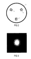
- FIG 2 shows the three LEDs 1 of FIG 1 that are now assumed to be equipped with a respective primary optics (e.g., a collimator, not shown) which shapes the light emitted from the respective LED 1.
- a respective primary optics e.g., a collimator, not shown
- Covering the LEDs 1 is a secondary optics in form of a Fresnel structure 2 is shown.
- the secondary optics 2 is acting upon the radiation patterns of all three LEDs 1. While the primary optics and the particular position of the LEDs 1 lead to a first multi-polar radiation pattern that is uniform in luminance after the primary optics, the secondary optics 2 redirects this light to change the luminance spot coming from the primary optics into a round spot with uniform luminance and uniform Correlated Colour Temperature, CCT. This is achieved because of the complete overlap of the single LED radiation patterns without shadowed areas or colour separation.
- CCT Correlated Colour Temperature
- FIG 3 shows a simulation result for the arrangement of FIG 2 of a light spot after the secondary optics 2.
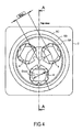
- FIG 4 shows a more detailed top-down view on the optical structure of the lighting device in an illustration basically similar to the one of FIG 2 .
- the primary optics includes a rotationally symmetric collimator body 4 that exhibits a respective maximum diameter Dcpc.
- three Fresnel rings 5A, 5B, 5C of the Fresnel structure 2 namely an inner Fresnel ring 5A, an intermediary Fresnel ring 5B and an outer Fresnel ring 5C.
- Rma denotes a distance from the optical axis (centre of symmetry) to the centre of the emitting area of a single LED that in this case coincides with the centre of the collimator 4. This value must be constant and depends on the number of light sources. Rma preferably is a multiple of the source emitting diameter Dcpc, particularly a double or triple value.
- FIG 5 shows the optical layers of FIG 4 in a cross-sectional side view along line A-A of FIG 5 .
- the primary optical layer comprises (from right to left) a substrate 5, on which the LEDs 1 are mounted. For the sake of clarity, electrical connections etc are not shown.
- Mounted on top of the LEDs 1 (to the left in FIG 6 ) is a respective collimator 4 that has a truncated conical body with a spherical top section.
- the shape of the primary Compound Parabolic Concentrator, CPC, ollimator 4 helps to increase the spot overlap and overlap of the radiation patterns, resp., after the primary collimation.
- the primary optics 4 are covered by a secondary optics layer 2 in form of the Fresnel structure 2.
- the Fresnel structure 2 shows the three Fresnel rings 5A, 5B, 5C having different heights with HLR denoting the height of the outermost Fresnel ring 5C.
- the diameter of the innermost Fresnel ring (central area) is denoted by Dmin,f.
- a pillow structure 6 Located within these rings 5A, 5B, 5C (central area) is a pillow structure 6 that faces the primary optics layer 1, 4.
- the pillow structure 6 optimizes the light spot's uniformity and avoids a colour separation.
- FIG 6 shows the LEDs 1 with their primary optics 4 and the Fresnel structure 2 with its Fresnel rings 5 in a perspective view.
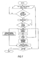
- an external dimension / shape of the primary optics is to be set. This is related to the value of a necessary etendue chosen to obtain a required radiation pattern. From the dimension / shape of the primary optics / lens follows the height Hcpc and the diameter of the primary collimator Dcpc that are both functions of the etendue. If this shape achieves the desired primary optics radiation pattern, the next step is it to define the distance Rma by taking into consideration Dcpc and the number of LED sources.
- k is proportional to n s .
- Rma gives the equidistance between sources. If the primary overlap of radiation patterns of the light sources is acceptable (e. g. no central areas of zero luminance, symmetry of the periphery / or of the external spot [not too elliptic] etc.) then the secondary optics is to be set / defined.
- the secondary optics that is located above the primary optics, consists of prismatic Fresnel rings and a pillow structure in the central area of it.
- the prismatic structure may then be designed as follows:
- the design of the prismatic structure is finished.
- the number of LED light sources is 3, that the required radiation pattern needs a full angle of 38° and that a spot uniformity is required, i. e., that there are no holes of luminance or colour separation after the secondary optics.
- the height of the last ring HLR should be in the range of 1 to 2 mm because the primary collimation caused by the collimator is assumed to be good.
- the pillow structure in the centre area of the secondary optics /Fresnel structure should be within the range of these values, e.g., such that a single pillow has the form of an ellipsoid with an hexagonal base of 1 mm and a height of about 0,5 - 1 mm, and a distance from the primary optics / collimator lens to a pillow being in the range of about 0,5 - 1,5 mm. If the primary optical system, including the LEDs and the collimator, exhibits a relatively large colour separation, the shape of the single pillow may be smaller and higher, for example.
- a lighting device using an optical system as shown in FIGs 1 to 6 provides inter alia the following advantages:
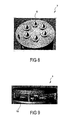
- FIGs 8 and 9 show different embodiments of a lighting system 7, 9, of which mainly the optics layers are shown.
- FIG 8 shows six collimators 8 in an angular symmetry around the optical axis
- FIG 9 shows six symmetrically arranged primary optics / collimators 10 of a yet different form.
- the invention is not limited to the above shown and described embodiments but is only limited by the claims.
- light emitting diodes instead of light emitting diodes, light emitting lasers can be used.
- shape of the primary optics may be different and may comprise different and more functions.
- the secondary structure may be different from a Fresnel structure and may not contain a pillow structure, or may comprise more or less then three Fresnel rings.
Landscapes
- Physics & Mathematics (AREA)
- General Physics & Mathematics (AREA)
- Optics & Photonics (AREA)
- Engineering & Computer Science (AREA)
- General Engineering & Computer Science (AREA)
- Non-Portable Lighting Devices Or Systems Thereof (AREA)
Abstract
Description
- The invention relates to a lighting device and a method for manufacturing a lighting device.
- Currently, multi-chip high-power/high-flux LED light sources are commonly coupled to optical structures like simple reflectors, standard optics, various lens arrays, or diffusive structures. These solutions offer limited performances in terms of efficiency, homogeneity of the resulting beam of light, and compactness.
- It is thus the object to provide a lighting device that overcomes some or all of the above stated problems.
- Under one aspect of the invention, the lighting device comprises multiple light sources each comprising a primary optics; and a secondary optics for the multiple light sources; such that at the secondary optics the radiation pattern emitted from the multiple light sources have a substantially uniform luminance; and such that the secondary optics transforms the radiation pattern from the multiple light sources into an elliptical - including circular - spot of light of substantially uniform luminance.
- The number of light sources is not limited. Every suitable light source can be used, like an incandescent light bulb, a light emitting diode or a laser diode. The use of LEDs is preferred. The primary optics can comprise a single optical element or multiple optical elements. Optical elements may be every element that is designed to alter the light emitted from the light source, e. g., including lenses, collimators, lightwave guides etc. The secondary optics can comprise a single optical element or multiple optical elements, or combinations thereof. An optical element may be any element that is designed to modify the light emitted from the light source, e. g., including Fresnel lenses, pillow structures, or combinations thereof.
- Advantageously, the multiple light sources are located in an angular symmetry around the optical axis of the lighting device.
- Advantageously, at the secondary optics the radiation patterns emitted from the multiple light sources are completely overlapping.
- Advantageously, the number of light sources is three or a multiple of three.
- Advantageously, three light sources are located at a centre of a respective side of an equilateral triangle.
- Advantageously, the light sources have an elongated (oblong) shape with the main longitudinal axis parallel to or coinciding with the respective side of the triangle. The shape may be rectangular or elliptic, for example
- Advantageously, the primary optics comprises a collimator.
- Advantageously, the secondary optics comprises a Fresnel structure.
- Advantageously, the Fresnel structure comprises a pillow structure within the area surrounded by the rings.
- Under another aspect of the invention, the method for manufacturing the lighting device comprises at least the following steps: defining a shape of the primary optics, comprising: comparing a radiation pattern of a single light source to a respective required radiation pattern; calculating a desired distance of the light source from an optical axis of the lighting device; and determining a satisfactory overlap of the radiation pattern of the single light sources; and the steps of: defining a shape of the secondary optics comprising: calculating a minimal diameter of Fresnel rings, a number of rings, and a geometry finalisation of a Fresnel structure; defining a shape of a pillow structure of the secondary optics; and comparing a final radiation pattern with a desired radiation pattern.
- The invention is schematically described in more detail in the following embodiments. Same or similar components are denotes by same reference signs, where applicable. This more detailed exemplary description is by no means intended to limit the invention.
- FIG 1
- shows a positioning of light sources of a lighting device according to the invention in a top-down view;
- FIG 2
- shows the light sources of
FIG 1 with an additional secondary optics in a top-down view; - FIG 3
- shows a simulation result of a light spot achieved by the arrangement of
FIG 2 in a top-down view; - FIG 4
- shows a top-down view on optical layers of the lighting device;
- FIG 5
- shows the optics layers of
FIG 4 in a cross-sectional side view along the line A-A ofFIG 5 ; - FIG 6
- shows the optics layers of the lighting device in a perspective view;
- FIG 7
- shows a flow chart describing a process of designing a lighting device according to the invention;
- FIG 8
- shows a perspective side view on another embodiment of a lighting device according to the invention;
- FIG 9
- shows a perspective side view on even another embodiment of a lighting device according to the invention.
-
FIG 1 shows the positions of three light emitting diodes (LEDs) 1 as light sources. TheLEDs 1 are located at respective centres of an equilateral triangle T. In the case shown theLEDs 1 are of rectangular form with the longer sides placed parallel to the respective side of the triangle T. This also represents an arrangement of theLEDs 1 having an angular three-fold symmetry (120°) around the centre of the triangle T. This positional arrangement creates a multi-polar radiation pattern from a completely overlapping superposition of the single LED radiation patterns RP. The overall radiation pattern thus has no discontinuities in it. -
FIG 2 shows the threeLEDs 1 ofFIG 1 that are now assumed to be equipped with a respective primary optics (e.g., a collimator, not shown) which shapes the light emitted from therespective LED 1. Covering theLEDs 1 is a secondary optics in form of a Fresnelstructure 2 is shown. Thesecondary optics 2 is acting upon the radiation patterns of all threeLEDs 1. While the primary optics and the particular position of theLEDs 1 lead to a first multi-polar radiation pattern that is uniform in luminance after the primary optics, thesecondary optics 2 redirects this light to change the luminance spot coming from the primary optics into a round spot with uniform luminance and uniform Correlated Colour Temperature, CCT. This is achieved because of the complete overlap of the single LED radiation patterns without shadowed areas or colour separation. -
FIG 3 shows a simulation result for the arrangement ofFIG 2 of a light spot after thesecondary optics 2. -
FIG 4 shows a more detailed top-down view on the optical structure of the lighting device in an illustration basically similar to the one ofFIG 2 . Additionally to the arrangement ofFIG 2 , there are now also shown theprimary optics 4. The primary optics includes a rotationallysymmetric collimator body 4 that exhibits a respective maximum diameter Dcpc. Also in more detail are shown threeFresnel rings structure 2, namely an inner Fresnelring 5A, an intermediary Fresnelring 5B and anouter Fresnel ring 5C. Rma denotes a distance from the optical axis (centre of symmetry) to the centre of the emitting area of a single LED that in this case coincides with the centre of thecollimator 4. This value must be constant and depends on the number of light sources. Rma preferably is a multiple of the source emitting diameter Dcpc, particularly a double or triple value. -
FIG 5 shows the optical layers ofFIG 4 in a cross-sectional side view along line A-A ofFIG 5 . The primary optical layer comprises (from right to left) asubstrate 5, on which theLEDs 1 are mounted. For the sake of clarity, electrical connections etc are not shown. Mounted on top of the LEDs 1 (to the left inFIG 6 ) is arespective collimator 4 that has a truncated conical body with a spherical top section. The shape of the primary Compound Parabolic Concentrator, CPC,ollimator 4 helps to increase the spot overlap and overlap of the radiation patterns, resp., after the primary collimation. - The
primary optics 4 are covered by asecondary optics layer 2 in form of theFresnel structure 2. TheFresnel structure 2 shows the three Fresnel rings 5A, 5B, 5C having different heights with HLR denoting the height of theoutermost Fresnel ring 5C. The diameter of the innermost Fresnel ring (central area) is denoted by Dmin,f. TheFresnel structure 2 with its predefined number (here: n = 3) and height of these reflective prisms (rings) 5A, 5B, 5C is able to redirect the light lost from theprimary optics - Located within these
rings pillow structure 6 that faces theprimary optics layer pillow structure 6 optimizes the light spot's uniformity and avoids a colour separation. -
FIG 6 shows theLEDs 1 with theirprimary optics 4 and theFresnel structure 2 with its Fresnel rings 5 in a perspective view. - The relation and setting of the shown parameters will now be explained in more detail with respect to
FIG 7 . For the sake of this example it is assumed that a certain number of CPC collimators placed in a correct location / mode are to be combined with one additional optical structure that includes a prismatic Fresnel ring and a certain remixing pillow structure, as, for example, shown inFIG 6 . - At first, an external dimension / shape of the primary optics is to be set. This is related to the value of a necessary etendue chosen to obtain a required radiation pattern. From the dimension / shape of the primary optics / lens follows the height Hcpc and the diameter of the primary collimator Dcpc that are both functions of the etendue. If this shape achieves the desired primary optics radiation pattern, the next step is it to define the distance Rma by taking into consideration Dcpc and the number of LED sources.

wherein k is a non dimensional factor of non-mechanical interference between primary optics and ns is a number of light sources. k is proportional to ns. Rma gives the equidistance between sources. If the primary overlap of radiation patterns of the light sources is acceptable (e. g. no central areas of zero luminance, symmetry of the periphery / or of the external spot [not too elliptic] etc.) then the secondary optics is to be set / defined. - In this case, the secondary optics, that is located above the primary optics, consists of prismatic Fresnel rings and a pillow structure in the central area of it. The prismatic structure may then be designed as follows:
- a) A minimum diameter Dmin,f is determined with a value so as not to interfere with correct light rays that create the required radiation pattern according to, e.g.,

- b) The number of prismatic rings nring depends on the primary optical loss or scattering effect and / or the non-interference between entrance optical surface and the LED source. This number is low for high efficient primary optics or high for low efficient primary optics and in this case, e.g., set to

- c) A maximum height of the outermost ring HLR depends on the light rays not collimated and may in this case, for example, be in the range of about 0,5 - 5 mm.
- d) A defined structure of pillows in the centre of the secondary optic / Fresnel structure is able to avoid colour separation or trip imaging. This factor should be optimized regarding pillow shape, diameter, height and distance to the primary optics.
- If the resulting radiation pattern sufficiently resembles the desired radiation pattern, the design of the prismatic structure is finished.
- Turning now to an even more concrete example, it is assumed that the number of LED light sources is 3, that the required radiation pattern needs a full angle of 38° and that a spot uniformity is required, i. e., that there are no holes of luminance or colour separation after the secondary optics.
- The dimension / optical shape for each single primary optic may be such that the height Hcpc may be in the range between 15 and 25 mm, especially about 20 mm, and the maximum diameter of the primary collimator Dcpc may also be in the range between 15 and 25 mm, especially about 21 mm. Due to the low number of light sources, one may take a low value of k. Therefore, Rma is:

- Now the secondary optics will be defined, starting from calculating the minimum diameter Dmin,f, namely

- The number of prismatic / Fresnel rings may be 3 due to an assumed high efficiency of the primary optical structure, i. e., nring = 3. The height of the last ring HLR should be in the range of 1 to 2 mm because the primary collimation caused by the collimator is assumed to be good. It follows that the pillow structure in the centre area of the secondary optics /Fresnel structure should be within the range of these values, e.g., such that a single pillow has the form of an ellipsoid with an hexagonal base of 1 mm and a height of about 0,5 - 1 mm, and a distance from the primary optics / collimator lens to a pillow being in the range of about 0,5 - 1,5 mm. If the primary optical system, including the LEDs and the collimator, exhibits a relatively large colour separation, the shape of the single pillow may be smaller and higher, for example.
- A lighting device using an optical system as shown in
FIGs 1 to 6 provides inter alia the following advantages: - Excellent white colour mixing with homogeneity and brightness and in CIE x-y colour coordinates (no colour separation);
- Compensation of characteristics of different light sources used in the same structure;
- A radiation pattern can be designed according to specification;
- High efficiency (only 18 % loss or less);
- Compact configuration;
- No multiple shadows are created after a certain relatively small distance from the secondary optics (e.g., 1 meter);
- Precisely defined radiation pattern;
- High tolerance against slight differences of white binning selection of the LED sources; and
- High tolerance against a non-circularity of the emitting area.
-
FIGs 8 and 9 show different embodiments of alighting system FIG 8 shows sixcollimators 8 in an angular symmetry around the optical axis, andFIG 9 shows six symmetrically arranged primary optics /collimators 10 of a yet different form. - The invention is not limited to the above shown and described embodiments but is only limited by the claims. For example, instead of light emitting diodes, light emitting lasers can be used. Also, the shape of the primary optics may be different and may comprise different and more functions. Further the secondary structure may be different from a Fresnel structure and may not contain a pillow structure, or may comprise more or less then three Fresnel rings.
-
- 1
- LED
- 2
- Fresnel structure
- 3
- 4
- collimator
- 5
- Fresnel ring
- 6
- pillow structure
- 7
- lighting system
- 8
- collimator
- 9
- lighting system
- 10
- collimator
- Dcpc
- maximum diameter of the collimator
- Dmin,f
- minimum diameter of the Fresnel rings
- Hcpc
- collimator height
- HLR
- height of an outermost Fresnel ring
- k
- interference factor
- nring
- number of Fresnel rings
- RP
- radiation pattern
- Rma
- distance
- T
- equilateral triangle
Claims (10)
- A lighting device (1-6;7;9), comprising- multiple light sources (1) each comprising a primary optics (4); and- a secondary optics (2) for the multiple light sources (1);- such that at the secondary optics (2) the radiation patterns (RP) emitted from the multiple light sources (2) have a substantially uniform luminance; and- such that the secondary optics (2) transforms the radiation pattern (RP) from the multiple light sources (1) into an elliptical spot of light of substantially uniform luminance.
- The lighting device (1-6;7;9) according to claim 1, wherein the multiple light sources (1) are located in an angular symmetry around an optical axis of the lighting device (7, 9).
- The lighting device (1-6;7;9) according to claim 1 or 2, wherein at the secondary optics (2) the radiation patterns (RP) emitted from the multiple light sources are completely overlapping.
- The lighting device (1-6;7;9) according to any of the preceding claims, wherein the number of light sources (1) is three or a multiple of three.
- The lighting device (1-6;7;9) according to any of the preceding claims, wherein three light sources (1) are located at a centre of a respective side of a equilateral triangle (T).
- The lighting device (1-6;7;9) according to claim 5, wherein the light sources (1) have an elongated shape with the longitudinal axis parallel to or coinciding with the respective side of the triangle (T).
- The lighting device (1-6;7;9) according to any of the preceding claims, wherein the primary optics comprises a collimator (4).
- The lighting device (1-6;7;9) according to any of the preceding claims, wherein the secondary optics comprises a Fresnel structure (2).
- The lighting device (1-6;7;9) according to claim 8, wherein the Fresnel structure (2) comprises a pillow structure (6) within the area surrounded by Fresnel rings (5).
- A method for manufacturing the lighting device (1-6;7;9) according to any of the preceding claims, the method comprising the steps of:- defining a shape of the primary optics (4), comprising:- comparing a radiation pattern (RP) of a single light source (1) to a respective required radiation pattern;- calculating a desired distance (Rma) of the light source (1) from an optical axis of the lighting device (7, 9); and- determining a satisfactory overlap of the radiation patterns (RP) of the single light sources; and- defining a shape of the secondary optics (2) comprising:- calculating a minimal diameter (Dmin,f) of Fresnel rings (5A-C), a number of Fresnel rings (nring), and a geometry finalisation of a Fresnel structure (2);- defining a shape of a pillow structure (6) of the secondary optics (2);- comparing a final radiation pattern (RP) with a desired radiation pattern.
Priority Applications (2)
| Application Number | Priority Date | Filing Date | Title |
|---|---|---|---|
| EP07010692A EP1998214B1 (en) | 2007-05-30 | 2007-05-30 | Lighting device |
| US12/129,762 US8622585B2 (en) | 2007-05-30 | 2008-05-30 | Lighting device with multiple light sources and primary and secondary optics |
Applications Claiming Priority (1)
| Application Number | Priority Date | Filing Date | Title |
|---|---|---|---|
| EP07010692A EP1998214B1 (en) | 2007-05-30 | 2007-05-30 | Lighting device |
Publications (2)
| Publication Number | Publication Date |
|---|---|
| EP1998214A1 true EP1998214A1 (en) | 2008-12-03 |
| EP1998214B1 EP1998214B1 (en) | 2012-10-10 |
Family
ID=38669438
Family Applications (1)
| Application Number | Title | Priority Date | Filing Date |
|---|---|---|---|
| EP07010692A Not-in-force EP1998214B1 (en) | 2007-05-30 | 2007-05-30 | Lighting device |
Country Status (2)
| Country | Link |
|---|---|
| US (1) | US8622585B2 (en) |
| EP (1) | EP1998214B1 (en) |
Cited By (1)
| Publication number | Priority date | Publication date | Assignee | Title |
|---|---|---|---|---|
| RU2615822C2 (en) * | 2015-05-19 | 2017-04-11 | Алексей Игоревич Салмин | Storage for information cases, which synchronizes auxiliary mixed laser lighting with area of intensive technical development, and nasal supports of sunglasses |
Families Citing this family (3)
| Publication number | Priority date | Publication date | Assignee | Title |
|---|---|---|---|---|
| US8662704B2 (en) * | 2009-08-14 | 2014-03-04 | U.S. Pole Company, Inc. | LED optical system with multiple levels of secondary optics |
| US10174906B2 (en) | 2012-06-18 | 2019-01-08 | Fresnel Technologies Inc. | LED luminaire tiling with a lens array containing a plurality of lenslets |
| CN110097804A (en) * | 2019-05-28 | 2019-08-06 | 大连大学 | A kind of study toning toy |
Citations (5)
| Publication number | Priority date | Publication date | Assignee | Title |
|---|---|---|---|---|
| WO2000036336A1 (en) * | 1998-12-17 | 2000-06-22 | Koninklijke Philips Electronics N.V. | Light engine |
| US6504650B1 (en) * | 1999-10-19 | 2003-01-07 | Anthony J. Alfrey | Optical transformer and system using same |
| WO2005050264A2 (en) * | 2003-11-18 | 2005-06-02 | Merlin Technologies, Inc. | Variable optical arrays and variable manufacturing methods |
| US20050174775A1 (en) * | 2004-02-11 | 2005-08-11 | 3M Innovative Properties Company | Light-collecting illumination system |
| EP1754997A1 (en) * | 2005-08-16 | 2007-02-21 | Kabushiki Kaisha Toshiba | Illuminator, LED illuminator, and imaging device with illuminator |
Family Cites Families (8)
| Publication number | Priority date | Publication date | Assignee | Title |
|---|---|---|---|---|
| US2853599A (en) * | 1956-05-17 | 1958-09-23 | Kliegl Bros Universal Electric | Oval beam lens |
| US5081637A (en) * | 1989-11-28 | 1992-01-14 | Massachusetts Institute Of Technology | Multiple-laser pump optical system |
| US6367949B1 (en) * | 1999-08-04 | 2002-04-09 | 911 Emergency Products, Inc. | Par 36 LED utility lamp |
| US7273987B2 (en) * | 2002-03-21 | 2007-09-25 | General Electric Company | Flexible interconnect structures for electrical devices and light sources incorporating the same |
| ITMI20030112A1 (en) * | 2003-01-24 | 2004-07-25 | Fraen Corp Srl | MULTIPLE OPTICAL ELEMENT FOR A LED LIGHTING DEVICE AND LED LIGHTING DEVICE INCLUDING SUCH OPTICAL ELEMENT. |
| US6864513B2 (en) * | 2003-05-07 | 2005-03-08 | Kaylu Industrial Corporation | Light emitting diode bulb having high heat dissipating efficiency |
| TWI255377B (en) * | 2004-11-05 | 2006-05-21 | Au Optronics Corp | Backlight module |
| US7310186B2 (en) | 2005-10-21 | 2007-12-18 | Hewlett-Packard Development Company, L.P. | Uniform multiple light source etendue |
-
2007
- 2007-05-30 EP EP07010692A patent/EP1998214B1/en not_active Not-in-force
-
2008
- 2008-05-30 US US12/129,762 patent/US8622585B2/en not_active Expired - Fee Related
Patent Citations (5)
| Publication number | Priority date | Publication date | Assignee | Title |
|---|---|---|---|---|
| WO2000036336A1 (en) * | 1998-12-17 | 2000-06-22 | Koninklijke Philips Electronics N.V. | Light engine |
| US6504650B1 (en) * | 1999-10-19 | 2003-01-07 | Anthony J. Alfrey | Optical transformer and system using same |
| WO2005050264A2 (en) * | 2003-11-18 | 2005-06-02 | Merlin Technologies, Inc. | Variable optical arrays and variable manufacturing methods |
| US20050174775A1 (en) * | 2004-02-11 | 2005-08-11 | 3M Innovative Properties Company | Light-collecting illumination system |
| EP1754997A1 (en) * | 2005-08-16 | 2007-02-21 | Kabushiki Kaisha Toshiba | Illuminator, LED illuminator, and imaging device with illuminator |
Cited By (1)
| Publication number | Priority date | Publication date | Assignee | Title |
|---|---|---|---|---|
| RU2615822C2 (en) * | 2015-05-19 | 2017-04-11 | Алексей Игоревич Салмин | Storage for information cases, which synchronizes auxiliary mixed laser lighting with area of intensive technical development, and nasal supports of sunglasses |
Also Published As
| Publication number | Publication date |
|---|---|
| US20080298057A1 (en) | 2008-12-04 |
| EP1998214B1 (en) | 2012-10-10 |
| US8622585B2 (en) | 2014-01-07 |
Similar Documents
| Publication | Publication Date | Title |
|---|---|---|
| US10295153B2 (en) | Optical system for producing uniform illumination | |
| US7850334B2 (en) | Apparatus and method of using multiple LED light sources to generate a unitized beam | |
| US8333488B2 (en) | Optical assembly having primary reflector and secondary reflector | |
| EP1753996B1 (en) | An apparatus and method for improved illumination area fill | |
| CN101802488B (en) | LED luminaire for illuminating a target plane | |
| EP2985512B1 (en) | Led unit module, light-emitting device, and light source system | |
| US10473292B2 (en) | Solid state illumination devices including spatially-extended light sources and reflectors | |
| EP2864694B1 (en) | Illumination device providing direct and indirect illumination | |
| US10859758B2 (en) | Illumination devices including multiple light emitting elements | |
| EP2721656B1 (en) | Led light source | |
| JP2014067716A (en) | Method and apparatus for providing uniform projection lighting | |
| KR20110135875A (en) | LED collimation optical module and lighting fixture using the same | |
| JP2016212962A (en) | Luminaire | |
| US10955111B2 (en) | Lens and lamp having a lens | |
| US8622585B2 (en) | Lighting device with multiple light sources and primary and secondary optics | |
| CN103511935A (en) | Lighting device | |
| EP2288847B1 (en) | Light output device and method | |
| US20140140069A1 (en) | Led illumination assemblies including partial lenses and metal reflectors | |
| KR20200082303A (en) | Optics device of head lamp and head lamp for vehicle using the same | |
| CN219453743U (en) | LED lamp | |
| WO2026073762A1 (en) | Freeform lens with convex outer surface and a convex-concave inner surface |
Legal Events
| Date | Code | Title | Description |
|---|---|---|---|
| PUAI | Public reference made under article 153(3) epc to a published international application that has entered the european phase |
Free format text: ORIGINAL CODE: 0009012 |
|
| AK | Designated contracting states |
Kind code of ref document: A1 Designated state(s): AT BE BG CH CY CZ DE DK EE ES FI FR GB GR HU IE IS IT LI LT LU LV MC MT NL PL PT RO SE SI SK TR |
|
| AX | Request for extension of the european patent |
Extension state: AL BA HR MK RS |
|
| 17P | Request for examination filed |
Effective date: 20090506 |
|
| AKX | Designation fees paid |
Designated state(s): AT BE BG CH CY CZ DE DK EE ES FI FR GB GR HU IE IS IT LI LT LU LV MC MT NL PL PT RO SE SI SK TR |
|
| 17Q | First examination report despatched |
Effective date: 20090821 |
|
| RIC1 | Information provided on ipc code assigned before grant |
Ipc: H01L 27/15 20060101ALI20120220BHEP Ipc: G09F 9/33 20060101ALI20120220BHEP Ipc: F21V 5/04 20060101ALI20120220BHEP Ipc: F21V 5/00 20060101ALI20120220BHEP Ipc: F21V 7/00 20060101ALI20120220BHEP Ipc: G02B 27/09 20060101AFI20120220BHEP Ipc: F21S 4/00 20060101ALI20120220BHEP |
|
| GRAP | Despatch of communication of intention to grant a patent |
Free format text: ORIGINAL CODE: EPIDOSNIGR1 |
|
| RAP1 | Party data changed (applicant data changed or rights of an application transferred) |
Owner name: OSRAM AG Owner name: OSRAM S.P.A. - SOCIETA' RIUNITE OSRAM EDISON CLERI |
|
| GRAS | Grant fee paid |
Free format text: ORIGINAL CODE: EPIDOSNIGR3 |
|
| GRAA | (expected) grant |
Free format text: ORIGINAL CODE: 0009210 |
|
| RAP1 | Party data changed (applicant data changed or rights of an application transferred) |
Owner name: OSRAM AG Owner name: OSRAM S.P.A. - SOCIETA' RIUNITE OSRAM EDISON CLERI |
|
| AK | Designated contracting states |
Kind code of ref document: B1 Designated state(s): AT BE BG CH CY CZ DE DK EE ES FI FR GB GR HU IE IS IT LI LT LU LV MC MT NL PL PT RO SE SI SK TR |
|
| REG | Reference to a national code |
Ref country code: GB Ref legal event code: FG4D |
|
| REG | Reference to a national code |
Ref country code: AT Ref legal event code: REF Ref document number: 579201 Country of ref document: AT Kind code of ref document: T Effective date: 20121015 Ref country code: CH Ref legal event code: EP |
|
| REG | Reference to a national code |
Ref country code: IE Ref legal event code: FG4D |
|
| REG | Reference to a national code |
Ref country code: DE Ref legal event code: R096 Ref document number: 602007025959 Country of ref document: DE Effective date: 20121213 |
|
| RAP2 | Party data changed (patent owner data changed or rights of a patent transferred) |
Owner name: OSRAM GMBH Owner name: OSRAM S.P.A. - SOCIETA' RIUNITE OSRAM EDISON CLERI |
|
| PG25 | Lapsed in a contracting state [announced via postgrant information from national office to epo] |
Ref country code: SI Free format text: LAPSE BECAUSE OF FAILURE TO SUBMIT A TRANSLATION OF THE DESCRIPTION OR TO PAY THE FEE WITHIN THE PRESCRIBED TIME-LIMIT Effective date: 20121010 |
|
| REG | Reference to a national code |
Ref country code: NL Ref legal event code: VDEP Effective date: 20121010 |
|
| REG | Reference to a national code |
Ref country code: AT Ref legal event code: MK05 Ref document number: 579201 Country of ref document: AT Kind code of ref document: T Effective date: 20121010 |
|
| REG | Reference to a national code |
Ref country code: LT Ref legal event code: MG4D |
|
| REG | Reference to a national code |
Ref country code: DE Ref legal event code: R081 Ref document number: 602007025959 Country of ref document: DE Owner name: OSRAM GMBH, DE Free format text: FORMER OWNER: OSRAM AG, 81543 MUENCHEN, DE Effective date: 20130205 |
|
| RAP2 | Party data changed (patent owner data changed or rights of a patent transferred) |
Owner name: OSRAM GMBH Owner name: OSRAM S.P.A. - SOCIETA' RIUNITE OSRAM EDISON CLERI |
|
| PG25 | Lapsed in a contracting state [announced via postgrant information from national office to epo] |
Ref country code: SE Free format text: LAPSE BECAUSE OF FAILURE TO SUBMIT A TRANSLATION OF THE DESCRIPTION OR TO PAY THE FEE WITHIN THE PRESCRIBED TIME-LIMIT Effective date: 20121010 Ref country code: ES Free format text: LAPSE BECAUSE OF FAILURE TO SUBMIT A TRANSLATION OF THE DESCRIPTION OR TO PAY THE FEE WITHIN THE PRESCRIBED TIME-LIMIT Effective date: 20130121 Ref country code: NL Free format text: LAPSE BECAUSE OF FAILURE TO SUBMIT A TRANSLATION OF THE DESCRIPTION OR TO PAY THE FEE WITHIN THE PRESCRIBED TIME-LIMIT Effective date: 20121010 Ref country code: FI Free format text: LAPSE BECAUSE OF FAILURE TO SUBMIT A TRANSLATION OF THE DESCRIPTION OR TO PAY THE FEE WITHIN THE PRESCRIBED TIME-LIMIT Effective date: 20121010 Ref country code: IS Free format text: LAPSE BECAUSE OF FAILURE TO SUBMIT A TRANSLATION OF THE DESCRIPTION OR TO PAY THE FEE WITHIN THE PRESCRIBED TIME-LIMIT Effective date: 20130210 Ref country code: LT Free format text: LAPSE BECAUSE OF FAILURE TO SUBMIT A TRANSLATION OF THE DESCRIPTION OR TO PAY THE FEE WITHIN THE PRESCRIBED TIME-LIMIT Effective date: 20121010 |
|
| PG25 | Lapsed in a contracting state [announced via postgrant information from national office to epo] |
Ref country code: BE Free format text: LAPSE BECAUSE OF FAILURE TO SUBMIT A TRANSLATION OF THE DESCRIPTION OR TO PAY THE FEE WITHIN THE PRESCRIBED TIME-LIMIT Effective date: 20121010 Ref country code: PL Free format text: LAPSE BECAUSE OF FAILURE TO SUBMIT A TRANSLATION OF THE DESCRIPTION OR TO PAY THE FEE WITHIN THE PRESCRIBED TIME-LIMIT Effective date: 20121010 Ref country code: CY Free format text: LAPSE BECAUSE OF FAILURE TO SUBMIT A TRANSLATION OF THE DESCRIPTION OR TO PAY THE FEE WITHIN THE PRESCRIBED TIME-LIMIT Effective date: 20121010 Ref country code: GR Free format text: LAPSE BECAUSE OF FAILURE TO SUBMIT A TRANSLATION OF THE DESCRIPTION OR TO PAY THE FEE WITHIN THE PRESCRIBED TIME-LIMIT Effective date: 20130111 Ref country code: PT Free format text: LAPSE BECAUSE OF FAILURE TO SUBMIT A TRANSLATION OF THE DESCRIPTION OR TO PAY THE FEE WITHIN THE PRESCRIBED TIME-LIMIT Effective date: 20130211 Ref country code: LV Free format text: LAPSE BECAUSE OF FAILURE TO SUBMIT A TRANSLATION OF THE DESCRIPTION OR TO PAY THE FEE WITHIN THE PRESCRIBED TIME-LIMIT Effective date: 20121010 |
|
| PG25 | Lapsed in a contracting state [announced via postgrant information from national office to epo] |
Ref country code: AT Free format text: LAPSE BECAUSE OF FAILURE TO SUBMIT A TRANSLATION OF THE DESCRIPTION OR TO PAY THE FEE WITHIN THE PRESCRIBED TIME-LIMIT Effective date: 20121010 |
|
| PG25 | Lapsed in a contracting state [announced via postgrant information from national office to epo] |
Ref country code: CZ Free format text: LAPSE BECAUSE OF FAILURE TO SUBMIT A TRANSLATION OF THE DESCRIPTION OR TO PAY THE FEE WITHIN THE PRESCRIBED TIME-LIMIT Effective date: 20121010 Ref country code: BG Free format text: LAPSE BECAUSE OF FAILURE TO SUBMIT A TRANSLATION OF THE DESCRIPTION OR TO PAY THE FEE WITHIN THE PRESCRIBED TIME-LIMIT Effective date: 20130110 Ref country code: DK Free format text: LAPSE BECAUSE OF FAILURE TO SUBMIT A TRANSLATION OF THE DESCRIPTION OR TO PAY THE FEE WITHIN THE PRESCRIBED TIME-LIMIT Effective date: 20121010 Ref country code: EE Free format text: LAPSE BECAUSE OF FAILURE TO SUBMIT A TRANSLATION OF THE DESCRIPTION OR TO PAY THE FEE WITHIN THE PRESCRIBED TIME-LIMIT Effective date: 20121010 Ref country code: SK Free format text: LAPSE BECAUSE OF FAILURE TO SUBMIT A TRANSLATION OF THE DESCRIPTION OR TO PAY THE FEE WITHIN THE PRESCRIBED TIME-LIMIT Effective date: 20121010 |
|
| PLBE | No opposition filed within time limit |
Free format text: ORIGINAL CODE: 0009261 |
|
| STAA | Information on the status of an ep patent application or granted ep patent |
Free format text: STATUS: NO OPPOSITION FILED WITHIN TIME LIMIT |
|
| PG25 | Lapsed in a contracting state [announced via postgrant information from national office to epo] |
Ref country code: RO Free format text: LAPSE BECAUSE OF FAILURE TO SUBMIT A TRANSLATION OF THE DESCRIPTION OR TO PAY THE FEE WITHIN THE PRESCRIBED TIME-LIMIT Effective date: 20121010 |
|
| 26N | No opposition filed |
Effective date: 20130711 |
|
| REG | Reference to a national code |
Ref country code: DE Ref legal event code: R081 Ref document number: 602007025959 Country of ref document: DE Owner name: OSRAM GMBH, DE Free format text: FORMER OWNER: OSRAM GMBH, 81543 MUENCHEN, DE Effective date: 20130829 |
|
| REG | Reference to a national code |
Ref country code: DE Ref legal event code: R097 Ref document number: 602007025959 Country of ref document: DE Effective date: 20130711 |
|
| PG25 | Lapsed in a contracting state [announced via postgrant information from national office to epo] |
Ref country code: MC Free format text: LAPSE BECAUSE OF FAILURE TO SUBMIT A TRANSLATION OF THE DESCRIPTION OR TO PAY THE FEE WITHIN THE PRESCRIBED TIME-LIMIT Effective date: 20121010 |
|
| REG | Reference to a national code |
Ref country code: CH Ref legal event code: PL |
|
| PG25 | Lapsed in a contracting state [announced via postgrant information from national office to epo] |
Ref country code: LI Free format text: LAPSE BECAUSE OF NON-PAYMENT OF DUE FEES Effective date: 20130531 Ref country code: CH Free format text: LAPSE BECAUSE OF NON-PAYMENT OF DUE FEES Effective date: 20130531 |
|
| REG | Reference to a national code |
Ref country code: IE Ref legal event code: MM4A |
|
| PG25 | Lapsed in a contracting state [announced via postgrant information from national office to epo] |
Ref country code: IE Free format text: LAPSE BECAUSE OF NON-PAYMENT OF DUE FEES Effective date: 20130530 |
|
| PG25 | Lapsed in a contracting state [announced via postgrant information from national office to epo] |
Ref country code: MT Free format text: LAPSE BECAUSE OF FAILURE TO SUBMIT A TRANSLATION OF THE DESCRIPTION OR TO PAY THE FEE WITHIN THE PRESCRIBED TIME-LIMIT Effective date: 20121010 |
|
| PG25 | Lapsed in a contracting state [announced via postgrant information from national office to epo] |
Ref country code: TR Free format text: LAPSE BECAUSE OF FAILURE TO SUBMIT A TRANSLATION OF THE DESCRIPTION OR TO PAY THE FEE WITHIN THE PRESCRIBED TIME-LIMIT Effective date: 20121010 |
|
| PG25 | Lapsed in a contracting state [announced via postgrant information from national office to epo] |
Ref country code: HU Free format text: LAPSE BECAUSE OF FAILURE TO SUBMIT A TRANSLATION OF THE DESCRIPTION OR TO PAY THE FEE WITHIN THE PRESCRIBED TIME-LIMIT; INVALID AB INITIO Effective date: 20070530 Ref country code: LU Free format text: LAPSE BECAUSE OF NON-PAYMENT OF DUE FEES Effective date: 20130530 |
|
| REG | Reference to a national code |
Ref country code: FR Ref legal event code: PLFP Year of fee payment: 10 |
|
| REG | Reference to a national code |
Ref country code: FR Ref legal event code: PLFP Year of fee payment: 11 |
|
| REG | Reference to a national code |
Ref country code: FR Ref legal event code: PLFP Year of fee payment: 12 |
|
| PGFP | Annual fee paid to national office [announced via postgrant information from national office to epo] |
Ref country code: IT Payment date: 20220524 Year of fee payment: 16 Ref country code: GB Payment date: 20220519 Year of fee payment: 16 Ref country code: FR Payment date: 20220523 Year of fee payment: 16 Ref country code: DE Payment date: 20220519 Year of fee payment: 16 |
|
| REG | Reference to a national code |
Ref country code: DE Ref legal event code: R119 Ref document number: 602007025959 Country of ref document: DE |
|
| GBPC | Gb: european patent ceased through non-payment of renewal fee |
Effective date: 20230530 |
|
| PG25 | Lapsed in a contracting state [announced via postgrant information from national office to epo] |
Ref country code: IT Free format text: LAPSE BECAUSE OF NON-PAYMENT OF DUE FEES Effective date: 20230530 Ref country code: DE Free format text: LAPSE BECAUSE OF NON-PAYMENT OF DUE FEES Effective date: 20231201 Ref country code: GB Free format text: LAPSE BECAUSE OF NON-PAYMENT OF DUE FEES Effective date: 20230530 |
|
| PG25 | Lapsed in a contracting state [announced via postgrant information from national office to epo] |
Ref country code: FR Free format text: LAPSE BECAUSE OF NON-PAYMENT OF DUE FEES Effective date: 20230531 |